EP2045849A2 - Leitfähige Substratstruktur mit kontrollierter Nanostäbchendichte und Herstellungsverfahren dafür - Google Patents
Leitfähige Substratstruktur mit kontrollierter Nanostäbchendichte und Herstellungsverfahren dafür Download PDFInfo
- Publication number
- EP2045849A2 EP2045849A2 EP08155641A EP08155641A EP2045849A2 EP 2045849 A2 EP2045849 A2 EP 2045849A2 EP 08155641 A EP08155641 A EP 08155641A EP 08155641 A EP08155641 A EP 08155641A EP 2045849 A2 EP2045849 A2 EP 2045849A2
- Authority
- EP
- European Patent Office
- Prior art keywords
- conductive substrate
- organic molecule
- nanorods
- seed layer
- phosphate
- Prior art date
- Legal status (The legal status is an assumption and is not a legal conclusion. Google has not performed a legal analysis and makes no representation as to the accuracy of the status listed.)
- Withdrawn
Links
- 239000000758 substrate Substances 0.000 title claims abstract description 168
- 239000002073 nanorod Substances 0.000 title claims abstract description 86
- 238000004519 manufacturing process Methods 0.000 title claims abstract description 13
- QAOWNCQODCNURD-UHFFFAOYSA-N Sulfuric acid Chemical compound OS(O)(=O)=O QAOWNCQODCNURD-UHFFFAOYSA-N 0.000 claims description 20
- 238000000034 method Methods 0.000 claims description 20
- 229910019142 PO4 Inorganic materials 0.000 claims description 18
- 239000010452 phosphate Substances 0.000 claims description 18
- ZOIORXHNWRGPMV-UHFFFAOYSA-N acetic acid;zinc Chemical compound [Zn].CC(O)=O.CC(O)=O ZOIORXHNWRGPMV-UHFFFAOYSA-N 0.000 claims description 17
- 239000004246 zinc acetate Substances 0.000 claims description 17
- NBIIXXVUZAFLBC-UHFFFAOYSA-K phosphate Chemical compound [O-]P([O-])([O-])=O NBIIXXVUZAFLBC-UHFFFAOYSA-K 0.000 claims description 16
- LFQSCWFLJHTTHZ-UHFFFAOYSA-N Ethanol Chemical compound CCO LFQSCWFLJHTTHZ-UHFFFAOYSA-N 0.000 claims description 15
- QAOWNCQODCNURD-UHFFFAOYSA-L Sulfate Chemical compound [O-]S([O-])(=O)=O QAOWNCQODCNURD-UHFFFAOYSA-L 0.000 claims description 12
- 150000003013 phosphoric acid derivatives Chemical class 0.000 claims description 11
- 150000003467 sulfuric acid derivatives Chemical class 0.000 claims description 11
- MHAJPDPJQMAIIY-UHFFFAOYSA-N Hydrogen peroxide Chemical compound OO MHAJPDPJQMAIIY-UHFFFAOYSA-N 0.000 claims description 10
- NBIIXXVUZAFLBC-UHFFFAOYSA-N Phosphoric acid Chemical compound OP(O)(O)=O NBIIXXVUZAFLBC-UHFFFAOYSA-N 0.000 claims description 10
- 125000000524 functional group Chemical group 0.000 claims description 10
- 239000000178 monomer Substances 0.000 claims description 8
- XOLBLPGZBRYERU-UHFFFAOYSA-N tin dioxide Chemical compound O=[Sn]=O XOLBLPGZBRYERU-UHFFFAOYSA-N 0.000 claims description 8
- 238000010438 heat treatment Methods 0.000 claims description 7
- 239000000203 mixture Substances 0.000 claims description 7
- 238000004528 spin coating Methods 0.000 claims description 7
- PYJJCSYBSYXGQQ-UHFFFAOYSA-N trichloro(octadecyl)silane Chemical compound CCCCCCCCCCCCCCCCCC[Si](Cl)(Cl)Cl PYJJCSYBSYXGQQ-UHFFFAOYSA-N 0.000 claims description 7
- NHTMVDHEPJAVLT-UHFFFAOYSA-N Isooctane Chemical compound CC(C)CC(C)(C)C NHTMVDHEPJAVLT-UHFFFAOYSA-N 0.000 claims description 6
- 238000000151 deposition Methods 0.000 claims description 6
- 230000008021 deposition Effects 0.000 claims description 6
- JVSWJIKNEAIKJW-UHFFFAOYSA-N dimethyl-hexane Natural products CCCCCC(C)C JVSWJIKNEAIKJW-UHFFFAOYSA-N 0.000 claims description 6
- 150000004756 silanes Chemical class 0.000 claims description 6
- 238000004544 sputter deposition Methods 0.000 claims description 6
- 229910000147 aluminium phosphate Inorganic materials 0.000 claims description 5
- 239000012298 atmosphere Substances 0.000 claims description 5
- QVGXLLKOCUKJST-UHFFFAOYSA-N atomic oxygen Chemical compound [O] QVGXLLKOCUKJST-UHFFFAOYSA-N 0.000 claims description 5
- 239000011521 glass Substances 0.000 claims description 5
- TVZISJTYELEYPI-UHFFFAOYSA-N hypodiphosphoric acid Chemical compound OP(O)(=O)P(O)(O)=O TVZISJTYELEYPI-UHFFFAOYSA-N 0.000 claims description 5
- 239000001301 oxygen Substances 0.000 claims description 5
- 229910052760 oxygen Inorganic materials 0.000 claims description 5
- 229910052751 metal Inorganic materials 0.000 claims description 4
- 239000002184 metal Substances 0.000 claims description 4
- 238000005119 centrifugation Methods 0.000 claims description 3
- 238000001035 drying Methods 0.000 claims description 3
- 239000012299 nitrogen atmosphere Substances 0.000 claims description 3
- 239000002245 particle Substances 0.000 claims description 3
- 238000010992 reflux Methods 0.000 claims description 2
- 238000005406 washing Methods 0.000 claims 1
- XLOMVQKBTHCTTD-UHFFFAOYSA-N Zinc monoxide Chemical compound [Zn]=O XLOMVQKBTHCTTD-UHFFFAOYSA-N 0.000 description 44
- 239000011787 zinc oxide Substances 0.000 description 22
- 239000000243 solution Substances 0.000 description 17
- 239000002105 nanoparticle Substances 0.000 description 15
- 239000000463 material Substances 0.000 description 7
- 229920000642 polymer Polymers 0.000 description 5
- 239000000047 product Substances 0.000 description 3
- 239000004065 semiconductor Substances 0.000 description 3
- GWEVSGVZZGPLCZ-UHFFFAOYSA-N Titan oxide Chemical compound O=[Ti]=O GWEVSGVZZGPLCZ-UHFFFAOYSA-N 0.000 description 2
- 230000008901 benefit Effects 0.000 description 2
- 230000015572 biosynthetic process Effects 0.000 description 2
- BASFCYQUMIYNBI-UHFFFAOYSA-N platinum Chemical compound [Pt] BASFCYQUMIYNBI-UHFFFAOYSA-N 0.000 description 2
- 238000004381 surface treatment Methods 0.000 description 2
- OKTJSMMVPCPJKN-UHFFFAOYSA-N Carbon Chemical compound [C] OKTJSMMVPCPJKN-UHFFFAOYSA-N 0.000 description 1
- 206010034972 Photosensitivity reaction Diseases 0.000 description 1
- BLRPTPMANUNPDV-UHFFFAOYSA-N Silane Chemical compound [SiH4] BLRPTPMANUNPDV-UHFFFAOYSA-N 0.000 description 1
- XUIMIQQOPSSXEZ-UHFFFAOYSA-N Silicon Chemical compound [Si] XUIMIQQOPSSXEZ-UHFFFAOYSA-N 0.000 description 1
- 239000011149 active material Substances 0.000 description 1
- 230000009286 beneficial effect Effects 0.000 description 1
- 229910052799 carbon Inorganic materials 0.000 description 1
- 239000000084 colloidal system Substances 0.000 description 1
- 150000001875 compounds Chemical class 0.000 description 1
- 230000003247 decreasing effect Effects 0.000 description 1
- 239000008151 electrolyte solution Substances 0.000 description 1
- 238000005516 engineering process Methods 0.000 description 1
- 238000005530 etching Methods 0.000 description 1
- 239000007789 gas Substances 0.000 description 1
- 239000012535 impurity Substances 0.000 description 1
- 229910003437 indium oxide Inorganic materials 0.000 description 1
- PJXISJQVUVHSOJ-UHFFFAOYSA-N indium(iii) oxide Chemical compound [O-2].[O-2].[O-2].[In+3].[In+3] PJXISJQVUVHSOJ-UHFFFAOYSA-N 0.000 description 1
- 238000001764 infiltration Methods 0.000 description 1
- 230000008595 infiltration Effects 0.000 description 1
- 239000002086 nanomaterial Substances 0.000 description 1
- 239000002070 nanowire Substances 0.000 description 1
- 239000012466 permeate Substances 0.000 description 1
- 125000002467 phosphate group Chemical group [H]OP(=O)(O[H])O[*] 0.000 description 1
- 230000001699 photocatalysis Effects 0.000 description 1
- 229910052697 platinum Inorganic materials 0.000 description 1
- 229910000077 silane Inorganic materials 0.000 description 1
- 229910052710 silicon Inorganic materials 0.000 description 1
- 239000010703 silicon Substances 0.000 description 1
- 239000010409 thin film Substances 0.000 description 1
- 230000007704 transition Effects 0.000 description 1
- 229910000314 transition metal oxide Inorganic materials 0.000 description 1
Images

Classifications
-
- H—ELECTRICITY
- H10—SEMICONDUCTOR DEVICES; ELECTRIC SOLID-STATE DEVICES NOT OTHERWISE PROVIDED FOR
- H10K—ORGANIC ELECTRIC SOLID-STATE DEVICES
- H10K30/00—Organic devices sensitive to infrared radiation, light, electromagnetic radiation of shorter wavelength or corpuscular radiation
- H10K30/80—Constructional details
- H10K30/81—Electrodes
- H10K30/82—Transparent electrodes, e.g. indium tin oxide [ITO] electrodes
-
- H—ELECTRICITY
- H10—SEMICONDUCTOR DEVICES; ELECTRIC SOLID-STATE DEVICES NOT OTHERWISE PROVIDED FOR
- H10K—ORGANIC ELECTRIC SOLID-STATE DEVICES
- H10K50/00—Organic light-emitting devices
- H10K50/80—Constructional details
- H10K50/805—Electrodes
- H10K50/81—Anodes
-
- Y—GENERAL TAGGING OF NEW TECHNOLOGICAL DEVELOPMENTS; GENERAL TAGGING OF CROSS-SECTIONAL TECHNOLOGIES SPANNING OVER SEVERAL SECTIONS OF THE IPC; TECHNICAL SUBJECTS COVERED BY FORMER USPC CROSS-REFERENCE ART COLLECTIONS [XRACs] AND DIGESTS
- Y02—TECHNOLOGIES OR APPLICATIONS FOR MITIGATION OR ADAPTATION AGAINST CLIMATE CHANGE
- Y02E—REDUCTION OF GREENHOUSE GAS [GHG] EMISSIONS, RELATED TO ENERGY GENERATION, TRANSMISSION OR DISTRIBUTION
- Y02E10/00—Energy generation through renewable energy sources
- Y02E10/50—Photovoltaic [PV] energy
- Y02E10/549—Organic PV cells
-
- Y—GENERAL TAGGING OF NEW TECHNOLOGICAL DEVELOPMENTS; GENERAL TAGGING OF CROSS-SECTIONAL TECHNOLOGIES SPANNING OVER SEVERAL SECTIONS OF THE IPC; TECHNICAL SUBJECTS COVERED BY FORMER USPC CROSS-REFERENCE ART COLLECTIONS [XRACs] AND DIGESTS
- Y02—TECHNOLOGIES OR APPLICATIONS FOR MITIGATION OR ADAPTATION AGAINST CLIMATE CHANGE
- Y02P—CLIMATE CHANGE MITIGATION TECHNOLOGIES IN THE PRODUCTION OR PROCESSING OF GOODS
- Y02P70/00—Climate change mitigation technologies in the production process for final industrial or consumer products
- Y02P70/50—Manufacturing or production processes characterised by the final manufactured product
Definitions
- the present invention relates to the solar cell or LED field, and more particularly, to a conductive substrate used as an electrode in the solar cell or LED field, and a method of manufacturing the conductive substrate.
- the present invention has been brought forth from research carried out as a part of the IT New Growth-driving Core Technology Development Project by the Ministry of Information and Telecommunications (Assignment Management No.: 2006-S-006-02, Assignment Name: Component/Module for Ubiquitous Terminal).
- Zinc oxide which is a binary oxide semiconductor that has a wurzite crystalline structure with a hexagonal system, is a direct transition group 3-5 compound semiconductor material, with a wide bandgap of 3.37eV and a high exciton binding energy at room temperature.
- Zinc oxide is used as a replacement material for indium oxide in flat-panel displays or used as a short-wave material at low voltage such as light-emitting devices and laser diodes, since zinc oxide is a material with high permissivity and refractive index and a large piezoelectric constant in the visible light region.
- the material is used in field emitting displays, or transparent electrodes, gas sensors, and UV screens of solar cells.
- the zinc oxide used in electronic devices was generally used in the form of a thin film, but currently it is used in the form of a nanorod or a nanowire. This is because, by forming a nanostructure, the critical emission current density can be increased, and thus, obtaining maximum efficiency, and when the zinc oxide nanorods are coated on a glass substrate, the photocatalytic efficiency can be enhanced to a maximum by increasing the area of exposure to a maximum.
- the conductive substrate is used very broadly as an electrode in fields such as the solar cells or LED (light-emitting diode) fields, and the conductive substrate acts as both a foundation for supporting an active layer and an electrode.
- a conductive substrate is subjected to various attempts to increase the surface area in contact with the active layer in order to enhance the efficiency of the cell.
- the evenness of the surface is controlled mostly at a micrometer level in order for the conductive substrate to increase its surface area, which also affects the transparency of the conductive substrate.
- the present invention provides a conductive substrate structure with controlled nanorod density so as to increase the contact between a conductive substrate structure and an active layer, and a method of manufacturing the conductive substrate structure.
- a conductive substrate structure with controlled nanorod density including: a base substrate, a conductive substrate formed on the base substrate and surface treated with an organic molecule; and nanorods grown from a seed layer applied on the conductive substrate, wherein the seed layer is applied only on a predetermined region of the conductive substrate by using the self-assembling characteristics of the organic molecule.
- the base substrate of the present invention may be a glass or a metal substrate, and the conductive substrate may be a transparent FTO (F-doped SnO 2 ) or ITO (InSO 2 ) substrate.
- the organic molecule may be one selected from the group consisting of silane series, phosphate series, sulfate series, and derivatives of a phosphate or a sulfate, wherein the phosphate series may include one functional group selected from the group consisting of phosphoric acid, phosphate, and hypophosphate; and the sulfate series may include one functional group selected from the group consisting of sulfuric acid, sulfate, and hyposulfate.
- the seed layer of the present invention may be ZnO, which may be applied on the conductive substrate with a method selected from the group consisting of heat deposition, sputtering, and spin coating. After the nanorods are grown, the organic molecule may be removed by a heat treatment at 250 °C under oxygen atmosphere, or using a mixture solution of hydrogen peroxide and sulfuric acid.
- the conductive substrate structure formed as such may have an expanded area of contact with the active layer by the nanorods with controlled density, and thereby be useful in organic solar cells or dye-sensitized nanocrystalline solar cells.
- a method of manufacturing a conductive substrate structure including: treating a conductive substrate formed on a base substrate with an organic molecule; applying a seed layer on a predetermined region of the conductive substrate by using the self-assembling characteristics of the organic molecule; and growing the nanorods with controlled density from the seed layer.
- the organic molecule of the present invention may be one selected from the group consisting of silane series, phosphate series, sulfate series, and derivatives of the phosphate or the sulfate, wherein the phosphate series may include one functional group selected from the group consisting of phosphoric acid, phosphate, and hypophosphate; and the sulfate series may include one functional group selected from the group consisting of sulfuric acid, sulfate, and hyposulfate.
- the organic molecule treatment may be carried out by immersing the conductive substrate in OTS isooctane solution for 1 to 2 minutes, and in the case where the organic molecule is a phosphate, the organic molecule treatment may be carried out by immersing the conductive substrate in the phosphate solution dissolved in alcohol for 20 to 30 minutes. After the organic molecule treatment, the conductive substrate may be washed with isooctane.
- OTS octadecyltrichlorosilane
- the seed layer of the present invention may be ZnO, which may be applied using a method selected from the group consisting of heat deposition, sputtering, and spin coating.
- the ZnO seed layer is prepared by baking 1.10g of zinc acetate dehydrate at 180°C for 1 hour, and then leaving the resulting product in 50mL of ethanol at 60°C for 30 minutes, and zinc acetate monomer solution for growing the nanorods is prepared by drying the zinc acetate dehydrate in nitrogen atmosphere, and then reflexing the resulting product in 50ml of ethanol at 60°C for 2 hours, subsequently removing the remaining particles through centrifugation.
- the nanorods are grown to about 1 to 2 ⁇ m by immersing the conductive substrate on which the ZnO seed layer is applied in the zinc acetate monomer solution for 24 hours or longer. After the nanorods are grown, the organic molecule is removed by a heat treatment under an oxygen atmosphere at 250 °C, or using a mixture solution of hydrogen peroxide and sulfuric acid.
- the conductive substrate structure according to the present invention with controlled nanorod density and a method of manufacturing the conductive substrate structure are capable of appropriately controlling the nanorod density by treating the conductive substrate with an organic molecule and then growing the nanorods, thereby significantly increasing the contact surface area between a conductive substrate and an active layer.
- the conductive substrate structure according to the present invention can be used effectively in organic solar cells or dye-sensitized nanocrystalline solar cells in which an efficient increase in the contact area is desired.
- a conductive substrate is used in organic solar cells and light-emitting diodes (LEDs), and the contact between the conductive substrate and an active material thereon is very important.
- Various methods are currently used in order to increase such contact area, among which changing the surface evenness by etching or the like is most common.
- the surface area of contact between the conductive substrate and an active layer includes a surface area of contact between nanorods formed on the conductive substrate and the active layer.
- the method of growing the nanorods has a very limited practical applicability due to excessively high density of the grown nanorods. That is, except for the case where the nanorods themselves are the active layer, when the nanorods density is high, the air layer amongst the nanorods cannot be easily extracted, or it is difficult to fill the space between the nanorods with the active layer, therefore increasing contact with the active layer is very limited.
- the contact area with polymers and the like may even be decreased. That is, at a high nanorod density, the polymers may not infiltrate the several-nanometer gap amongst the nanorods, and thus, forming only an air gap therein, and in turn reducing the contact area.
- the active layer material is mostly a polymer structure or a colloid mixed with nanoparticles, not readily capable of infiltrating amongst the nanorods.
- nanorods are not beneficial if the nanorod density is not appropriately controlled. If the gaps amongst the nanorods can be controlled, air gap formation can be prevented just by adjusting the gaps, and the contact formation between the nanorods and the active layer can be easily achieved. Therefore, controlling the nanorod density is very important with regards to conductive substrates using nanorods.
- FIG. 1 is a cross-sectional view of a conductive substrate structure with controlled nanorods density, according to an embodiment of the present invention.
- the conductive substrate structure includes a base substrate 100, a conductive substrate 200 on the base substrate 100, and nanorods 300 formed on the conductive substrate 200.
- the base substrate 100 may be a glass or metal-based substrate
- the conductive substrate 200 may be an FTO (F-doped SnO 2 ) or ITO (InSnO 2 )-based substrate.
- FTO F-doped SnO 2
- ITO InSnO 2
- such a conductive substrate 200 undergoes organic molecule treatment before the nanorod 300 growth, and this is performed in order for the nanorods 300 to grow with an appropriate density on the conductive substrate 200.
- the nanorods 300 are grown by a seed layer applied on the conductive substrate 200 to a length of 1 to 2 ⁇ m, and by treating the conductive substrate 200 with an organic molecule, the seed layer is applied to only a predetermined region of the conductive substrate according to the self-assembling properties of the organic molecule. Accordingly, the nanorods 300 grown from the seed layer are grown at an appropriately controlled spots depending on the position of the seeds. That is, by treating the conductive substrate 200 with the organic molecule, the conductive substrate 200 whereon nanorods 300 are formed at an appropriate density can be implemented.
- the organic molecule may include silane series, phosphate series, sulfate series, or a derivative of the phosphate or the sulfate.
- the organic molecule including a phosphate series may be a phosphoric acid, or its corresponding functional groups such as phosphate or hypophosphate
- the organic molecule including a sulfate series may be a sulfuric acid or its corresponding functional group such as sulfate or hyposulfate.
- the self-assembling degree of the organic molecule on the conductive substrate can be controlled.
- an appropriate seed layer such as ZnO seed layer may be applied only on areas where the organic molecule is not present.
- the application of the seed layer may be carried out using heat deposition, sputtering, or spin coating.
- the nanorods 300 are grown from the seed layer applied on a predetermined area, such that the density of the nanorods 300 is automatically controlled, and thereby enabling the implementation of a conductive substrate with the density of the nanorods 300 controller, Also, following the growth of the nanorods 300, an active layer such as an active layer of nanoparticles are applied over the conductive substrate 200, in which the organic molecule present on the conductive substrate 200 is removed by heat treating at 250°C under an oxygen atmosphere before or after applying the nanoparticles. Moreover, besides the heat treatment, the organic molecule may also be removed by immersing the conductive substrate 200 in a mixture solution of hydrogen peroxide and sulfuric acid. When the organic molecule is removed, only the nanorods 300 with a controlled density exist on the conductive substrate 200.
- the conductive substrate structure with controlled nanorod density according to the present invention is capable of appropriately controlling the nanorod density by treating the conductive substrate with an organic molecule and then growing the nanorods, thereby significantly increasing the contact surface area between the conductive substrate and the active layer. Therefore, the conductive substrate structure according to the present invention can be used effectively in organic solar cells or dye-sensitized nanocrystalline solar cells in which an efficient increase in the contact area is desired.
- FIG. 2 is a cross-sectional view of schematically illustrating an active layer being applied to the conductive substrate structure of FIG. 1 .
- the active layer such as an active layer of nanoparticles 400 is applied on the conductive substrate structure of FIG. 1 with controlled density of the nanorods 300.
- Such nanoparticles 400 are used in a dye-sensitized nanocrystalline solar cell and the like as the active layer on the conductive substrate 200.
- the dye-sensitized nanocrystalline solar cell in contrast to a silicon-based solar cell employing a conventional p-n connection, is a photoelectrochemical solar cell of which main materials include a photosensitized dye molecule capable of producing an electron-hole pair by absorbing visible light, and a transition metal oxide transferring produced electrons.
- a representative example of a dye-sensitized nanocrystalline solar cell known to date is disclosed by Gratzel et. al. of Switzerland ( U.S. Patent Laid-open Publication Nos. 4,927,721 and 5,350,644 ).
- the dye-sensitized nanocrystalline solar cell suggested by Gratzel et. al. is composed of a semiconductor electrode made of TiO 2 nanoparticles with dye molecules adsorbed thereto, and a counter electrode coated with platinum or carbon, and an electrolyte solution filled between the electrodes.
- the nanorods 300 on the conductive substrate 200 of the present embodiment are formed at a relatively low density, that is, with relatively wide gaps between the nanorods 300, in which the nanoparticles 400 are filled amongst the nanorods 300, and thus, the area of contact between the nanoparticles 400 and the conductive substrate 200 can be increased.
- the present embodiment introduces nanoparticles as an active layer, but the active layer is not limited thereto.
- the conductive substrate 200 of the present embodiment has a low nanorod density, even if a polymer is used as the active layer, the polymeric active layer can conveniently permeate amongst the nanorods 300, and thus, maintaining an increased contact area with the conductive substrate 200.
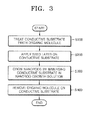
- FIG. 3 is a flowchart illustrating a method of manufacturing the conductive substrate structure of FIG. 1 , according to an embodiment of the present invention.
- the conductive substrate 200 formed on the base substrate 100 is first treated with an organic molecule (S100), where the organic molecule may be silane series, phosphate series, sulfate series, or a derivative of the phosphate or the sulfate, as previously described.
- a silane such as OTS (octadecyltrichlorosilane) is used in the present embodiment. That is, a 20mM OTS isooctane solution is prepared, in which the conductive substrate 200 is immersed for 1 to 2 minutes for surface treatment.
- the phosphate is dissolved in alcohol to prepare an alcohol-phosphate mixture solution, in which the conductive substrate 200 is immersed for 20 to 30 minutes for surface treatment.
- the surface of the conductive substrate 200 treated with the organic molecule as such may further be washed with an isooctane solution in order to remove any impurities or incompletely applied organic molecules.
- the organic molecule is only applied to a predetermined area of the conductive substrate 200 due to the self-assembling properties of the organic molecule.
- concentration of the organic molecule or the treatment time can be appropriately adjusted without being limited to the conditions described above, so as to apply the organic molecule to the conductive substrate 200 with a suitable density.
- a seed layer such as a ZnO seed layer is applied on the conductive substrate 200 (S200).
- the ZnO seed layer can be applied using various methods such as heat deposition, sputtering, or spin coating.
- the ZnO seed may be formed by baking 1.10g of zinc acetate dehydrate at 180°C for 1 hour, and leaving the resulting product in 50 ml of ethanol at 60°C for 30 minutes.
- the ZnO seed layer is applied only on the parts where the organic molecule is absent. That is, as previously described, the organic molecule is applied only to a predetermined area according to its self-assembling characteristics, and the ZnO seed layer, having a low binding capacity with such organic molecule, is only applied to the conductive substrate 200 on the area not covered by the organic molecule. Accordingly, the ZnO seed layer is applied on the conductive substrate 200 in an automatic degree of controlled density.
- the conductive substrate 200, on which the ZnO seed layer is applied, is hardened at about 200°C, and the conductive substrate 200 is immersed in a nanorod growth solution to grow the nanorods 300 (S300).
- the solution used to grow the nanorods 300 may be zinc acetate monomer solution, since the seed layer uses ZnO.
- Such zinc acetate monomer solution may be prepared by drying zinc acetate under nitrogen atmosphere, and then refluxing the zinc acetate in 50ml of ethanol at 60°C for 2 hours, and removing the remaining particles through centrifugation.
- the zinc acetate monomer solution prepared as such may be stored at a temperature lower than or equal to 5°C
- the nanorods 300 can be grown to about 1 to 2 ⁇ m by immersing the conductive substrate 200 on which the ZnO seed layer is applied in the zinc acetate monomer solution for 24 hours or longer, so that the nanorods 300 of desired length can be obtained by selecting an appropriate growth time.
- the organic molecule existing on the conductive substrate 200 is removed (S400).
- the organic molecule can be removed, before or after applying an active layer, such as the nanoparticles 400 or polymers, on the conductive substrate 200 after the growth of the nanorods 300, by a heat-treatment under an oxygen atmosphere at 250°C.
- an active layer such as the nanoparticles 400 or polymers
- the organic molecule can be removed by immersing the conductive substrate 200 in a mixture solution of hydrogen peroxide and sulfuric acid.
- the method of manufacturing the conductive substrate structure according to the present invention is capable of appropriately controlling the nanorod density by treating the conductive substrate with an organic molecule and then growing the nanorods, thereby significantly increasing the contact surface area between a conductive substrate and an active layer.
- the conductive substrate structure manufactured according to the present invention can be used effectively in organic solar cells or dye-sensitized nanocrystalline solar cells in which an efficient increase in the contact area is desired.
- the present invention provides a conductive substrate structure with controlled nanorod density so that the contact between a conductive substrate and an active layer can be expanded, and a method of manufacturing the conductive substrate structure.
- the conductive substrate structure includes: a base substrate, and a conductive substrate formed on the base substrate, and surface treated with an organic molecule; and nanorods grown from a seed layer applied on the conductive substrate, wherein the seed layer is applied only on a predetermined region of the conductive substrate by using the self-assembling characteristics of the organic molecule, and thus, controlling the density of the nanorods.
- the method of manufacturing the substrate structure includes: treating a conductive substrate, formed on top of a base substrate, with an organic molecule; applying the seed layer only to a predetermined region of the conductive substrate by using the self-assembling characteristics of the organic molecules; and growing nanorods with a controlled density from the seed layer.
Landscapes
- Physics & Mathematics (AREA)
- Optics & Photonics (AREA)
- Electromagnetism (AREA)
- Hybrid Cells (AREA)
- Photovoltaic Devices (AREA)
Applications Claiming Priority (1)
| Application Number | Priority Date | Filing Date | Title |
|---|---|---|---|
| KR1020070098886A KR100932903B1 (ko) | 2007-10-01 | 2007-10-01 | 나노로드 밀집도가 조절된 전도성 기판 구조체 및 그전도성 기판 구조체 제조 방법 |
Publications (1)
| Publication Number | Publication Date |
|---|---|
| EP2045849A2 true EP2045849A2 (de) | 2009-04-08 |
Family
ID=39876781
Family Applications (1)
| Application Number | Title | Priority Date | Filing Date |
|---|---|---|---|
| EP08155641A Withdrawn EP2045849A2 (de) | 2007-10-01 | 2008-05-05 | Leitfähige Substratstruktur mit kontrollierter Nanostäbchendichte und Herstellungsverfahren dafür |
Country Status (2)
| Country | Link |
|---|---|
| EP (1) | EP2045849A2 (de) |
| KR (1) | KR100932903B1 (de) |
Cited By (2)
| Publication number | Priority date | Publication date | Assignee | Title |
|---|---|---|---|---|
| TWI605609B (zh) * | 2017-03-13 | 2017-11-11 | Ultraviolet light sensing element and its manufacturing method | |
| CN112951956A (zh) * | 2021-03-12 | 2021-06-11 | 广东先导稀材股份有限公司 | 一种GaN基LED外延片及其制备方法 |
Families Citing this family (3)
| Publication number | Priority date | Publication date | Assignee | Title |
|---|---|---|---|---|
| KR101564330B1 (ko) | 2009-10-15 | 2015-10-29 | 삼성전자주식회사 | 유기 나노와이어를 포함하는 태양전지 |
| KR101642376B1 (ko) * | 2010-04-14 | 2016-07-26 | 도레이첨단소재 주식회사 | 이산화티탄 나노입자에 산화아연 나노막대를 혼합시킨 염료감응형 태양전지용 페이스트의 제조방법 |
| KR101974581B1 (ko) * | 2012-09-24 | 2019-05-02 | 삼성전자주식회사 | 3차원 나노플라즈모닉 구조체 및 이의 제조방법 |
Citations (2)
| Publication number | Priority date | Publication date | Assignee | Title |
|---|---|---|---|---|
| US4927721A (en) | 1988-02-12 | 1990-05-22 | Michael Gratzel | Photo-electrochemical cell |
| US5350644A (en) | 1990-04-17 | 1994-09-27 | Ecole Polytechnique, Federale De Lausanne | Photovoltaic cells |
Family Cites Families (3)
| Publication number | Priority date | Publication date | Assignee | Title |
|---|---|---|---|---|
| KR100548017B1 (ko) * | 2003-05-22 | 2006-01-31 | 한국과학기술원 | 나노미터 또는 그 이하 사이즈의 패턴 형성방법 |
| JP2006342040A (ja) * | 2005-05-09 | 2006-12-21 | Kumamoto Univ | 筒状分子構造およびその製造方法、並びに前処理基板およびその製造方法 |
| JP2007000727A (ja) * | 2005-06-22 | 2007-01-11 | Mitsubishi Rayon Eng Co Ltd | 膜分離活性汚泥処理装置の運転方法 |
-
2007
- 2007-10-01 KR KR1020070098886A patent/KR100932903B1/ko not_active Expired - Fee Related
-
2008
- 2008-05-05 EP EP08155641A patent/EP2045849A2/de not_active Withdrawn
Patent Citations (2)
| Publication number | Priority date | Publication date | Assignee | Title |
|---|---|---|---|---|
| US4927721A (en) | 1988-02-12 | 1990-05-22 | Michael Gratzel | Photo-electrochemical cell |
| US5350644A (en) | 1990-04-17 | 1994-09-27 | Ecole Polytechnique, Federale De Lausanne | Photovoltaic cells |
Cited By (2)
| Publication number | Priority date | Publication date | Assignee | Title |
|---|---|---|---|---|
| TWI605609B (zh) * | 2017-03-13 | 2017-11-11 | Ultraviolet light sensing element and its manufacturing method | |
| CN112951956A (zh) * | 2021-03-12 | 2021-06-11 | 广东先导稀材股份有限公司 | 一种GaN基LED外延片及其制备方法 |
Also Published As
| Publication number | Publication date |
|---|---|
| KR20090033712A (ko) | 2009-04-06 |
| KR100932903B1 (ko) | 2009-12-21 |
Similar Documents
| Publication | Publication Date | Title |
|---|---|---|
| Qiu et al. | Solution-derived 40 µm vertically aligned ZnO nanowire arrays as photoelectrodes in dye-sensitized solar cells | |
| Vogel et al. | Quantum-sized PbS, CdS, Ag2S, Sb2S3, and Bi2S3 particles as sensitizers for various nanoporous wide-bandgap semiconductors | |
| CN108389977A (zh) | 一种钙钛矿太阳能电池及其制备方法 | |
| Hao et al. | A novel semiconductor-sensitized solar cell based on P3HT@ CdS@ TiO2 core-shell nanotube array | |
| CN101916670B (zh) | 一种TiO2纳米花薄膜光阳极及其制备方法 | |
| CN107195789A (zh) | 一种无机混合卤素钙钛矿薄膜的制备方法及其在制备太阳能电池方面的应用 | |
| EP2045849A2 (de) | Leitfähige Substratstruktur mit kontrollierter Nanostäbchendichte und Herstellungsverfahren dafür | |
| CN106960883A (zh) | 一种全无机钙钛矿太阳能电池及其制备方法 | |
| CN102544373B (zh) | 一种量子点敏化有序体异质结太阳电池及其制备方法 | |
| CN104282847A (zh) | 一种可扰式钙钛矿型有机卤化物薄膜太阳能电池光阳极制备方法 | |
| CN101049957A (zh) | 一种溶液法制备不同形貌纳米氧化锌薄膜的方法 | |
| KR101087266B1 (ko) | 실리콘 나노와이어/징크옥사이드 코어/쉘 나노복합체의 제조방법 및 상기 나노복합체를 포함하는 태양전지 | |
| KR20170051673A (ko) | 금속 산화물 나노섬유, 나노막대 및 코팅층을 광전극으로 포함하는 페로브스카이트 태양전지 및 이의 제조방법 | |
| CN108545960A (zh) | 一种Y掺杂ZnO纳米棒阵列制备方法 | |
| Han et al. | Efficient promotion of charge separation and suppression of charge recombination by blending PCBM and its dimer as electron transport layer in inverted perovskite solar cells | |
| CN108550706B (zh) | 一种量子点光电探测器的制备方法 | |
| Chen et al. | Fabrication of silver sulfide thin films for efficient organic solar cells with high short-circuit currents based on double heterojunctions | |
| CN113644202A (zh) | 一种自发定向成膜法制备的有机太阳能电池及其制备方法 | |
| CN112510150A (zh) | 空穴传输层及其制备方法和应用 | |
| CN104746119A (zh) | 一种ZnO纳米材料以及合成ZnO纳米材料的方法 | |
| KR101282291B1 (ko) | 산화아연 요철구조의 형성방법 및 이를 이용한 태양전지의 제조방법 | |
| JP2024541143A (ja) | 抵抗増強用ナノ構造のキャリア輸送層を有するペロブスカイト-結晶シリコン積層電池 | |
| US7622397B2 (en) | InN/TiO2 photosensitized electrode | |
| KR101069066B1 (ko) | 알루미늄이 도핑된 산화아연 나노로드 기반 실리콘 태양전지의 투명전도성기판 제조방법 | |
| CN108878660A (zh) | 一种Ag/ZnO核壳结构纳米棒阵列电极材料制备方法 |
Legal Events
| Date | Code | Title | Description |
|---|---|---|---|
| PUAI | Public reference made under article 153(3) epc to a published international application that has entered the european phase |
Free format text: ORIGINAL CODE: 0009012 |
|
| AK | Designated contracting states |
Kind code of ref document: A2 Designated state(s): AT BE BG CH CY CZ DE DK EE ES FI FR GB GR HR HU IE IS IT LI LT LU LV MC MT NL NO PL PT RO SE SI SK TR |
|
| AX | Request for extension of the european patent |
Extension state: AL BA MK RS |
|
| STAA | Information on the status of an ep patent application or granted ep patent |
Free format text: STATUS: THE APPLICATION HAS BEEN WITHDRAWN |
|
| 18W | Application withdrawn |
Effective date: 20140903 |