EP2044424B1 - Procédé pour fabriquer un détecteur de gaz présentant des nanostructures d'oxyde de zinc - Google Patents
Procédé pour fabriquer un détecteur de gaz présentant des nanostructures d'oxyde de zinc Download PDFInfo
- Publication number
- EP2044424B1 EP2044424B1 EP07745782A EP07745782A EP2044424B1 EP 2044424 B1 EP2044424 B1 EP 2044424B1 EP 07745782 A EP07745782 A EP 07745782A EP 07745782 A EP07745782 A EP 07745782A EP 2044424 B1 EP2044424 B1 EP 2044424B1
- Authority
- EP
- European Patent Office
- Prior art keywords
- zinc oxide
- oxide nano
- metal
- structures
- solution
- Prior art date
- Legal status (The legal status is an assumption and is not a legal conclusion. Google has not performed a legal analysis and makes no representation as to the accuracy of the status listed.)
- Not-in-force
Links
Images

Classifications
-
- G—PHYSICS
- G01—MEASURING; TESTING
- G01N—INVESTIGATING OR ANALYSING MATERIALS BY DETERMINING THEIR CHEMICAL OR PHYSICAL PROPERTIES
- G01N27/00—Investigating or analysing materials by the use of electric, electrochemical, or magnetic means
- G01N27/02—Investigating or analysing materials by the use of electric, electrochemical, or magnetic means by investigating impedance
- G01N27/04—Investigating or analysing materials by the use of electric, electrochemical, or magnetic means by investigating impedance by investigating resistance
- G01N27/12—Investigating or analysing materials by the use of electric, electrochemical, or magnetic means by investigating impedance by investigating resistance of a solid body in dependence upon absorption of a fluid; of a solid body in dependence upon reaction with a fluid, for detecting components in the fluid
-
- B—PERFORMING OPERATIONS; TRANSPORTING
- B82—NANOTECHNOLOGY
- B82Y—SPECIFIC USES OR APPLICATIONS OF NANOSTRUCTURES; MEASUREMENT OR ANALYSIS OF NANOSTRUCTURES; MANUFACTURE OR TREATMENT OF NANOSTRUCTURES
- B82Y15/00—Nanotechnology for interacting, sensing or actuating, e.g. quantum dots as markers in protein assays or molecular motors
-
- Y—GENERAL TAGGING OF NEW TECHNOLOGICAL DEVELOPMENTS; GENERAL TAGGING OF CROSS-SECTIONAL TECHNOLOGIES SPANNING OVER SEVERAL SECTIONS OF THE IPC; TECHNICAL SUBJECTS COVERED BY FORMER USPC CROSS-REFERENCE ART COLLECTIONS [XRACs] AND DIGESTS
- Y10—TECHNICAL SUBJECTS COVERED BY FORMER USPC
- Y10T—TECHNICAL SUBJECTS COVERED BY FORMER US CLASSIFICATION
- Y10T29/00—Metal working
- Y10T29/49—Method of mechanical manufacture
- Y10T29/49002—Electrical device making
Definitions
- the present invention relates to a method of fabricating a gas sensor having zinc oxide nano-structures, and more particularly, to a method of fabricating a high-sensitivity gas sensor capable of detecting a variety of gases using zinc oxide nano-structures and metal islands coated on the zinc oxide nano-structures.
- Rout et al. (Chem. Phys. Lett. 418 (2006) 586-590 ) describes a method of fabricating a gas sensor based on zinc oxide nanowires, wherein the nanowires are ground with a diethylene glycol and the paste obtained is coated onto an alumina substrate. The paste is then impregnated with a chloroplatinate solution and the paste finally sintered at 400°C.
- Tien et al. discloses a method of fabricating a gas sensor, wherein zinc oxide nanowires are coated with discontinuous Pt clusters by sputter coating.
- the present invention provides a method of fabricating a gas sensor by which a high-sensitivity gas sensor can be fabricated at low cost using a simpler fabricating process.
- the gas sensor thus fabricated includes: a plurality of zinc oxide nano-structures formed on a substrate; a plurality of metal islands coated on a surface of each zinc oxide nano-structure and separated from one another; a first electrode electrically connected to one end of each zinc oxide nano-structure through the substrate; a second electrode electrically connected to the other end of each zinc oxide nano-structure; and a current variation-measuring unit electrically connected to each of the first electrode and the second electrode so as to measure a variation in the amount of current flowing between the first electrode and the second electrode.
- Each zinc oxide nano-structure may have a structure of a nano-wire or nano-rod.
- the metal islands may be formed of one material selected from the group consisting of platinum (Pt), palladium (Pd), nickel (Ni), and cobalt (Co).
- a method of fabricating a gas sensor In the method, a plurality of metal islands separated from one another on a surface of each of a plurality of zinc oxide nano-structures are formed by coating metal components of a metal material on the surface of each zinc oxide nano-structure in a solution in which the metal material is solved. And, a first electrode to be electrically connected to ends of the zinc oxide nano-structures and a second electrode to be electrically connected to the other ends of the zinc oxide nano-structures are formed.
- the method may further include, before forming the first electrode and the
- the solution may include the metal material solved in aqua regia.
- solution may further include at least one selected from distilled water and basic solution.
- the metal material may be a metal powder or a metal organic compound.
- the method may further include, before forming the plurality of metal islands ,
- the forming of the plurality of metal islands includes dipping the substrate on which the zinc oxide nano-structures are formed in the solution.
- a plurality of metal islands are formed on a zinc oxide nano-structure and are independently separated from one another on the zinc oxide nano-structure and sensitivity to a gas is improved by the metal islands such that a variety of kinds of gases can be detected.
- a wet method is used to form the metal islands on the surface of the zinc oxide nano-structure.
- FIG. 1 is a schematic perspective view of a gas sensor
- FIG. 2 is a perspective view of a single zinc oxide nano-structure of the gas sensor of FIG. 1 ;
- FIG. 3 is a flowchart illustrating a method of fabricating a gas sensor according to an embodiment of the present invention.
- FIG. 1 is a schematic perspective view of a gas sensor 10.
- the gas sensor 10 of FIG. 1 includes a plurality of zinc oxide nano-structures 14 formed on a main surface of a substrate 12.
- the substrate 12 may be a silicon substrate.
- Each zinc oxide nano-structure 14 may have a structure of a nano-wire or nano-rod.
- Each zinc oxide nano-structure 14 may have a diameter of about several tens to several hundreds of nm, for example, from about 10 to 900 nm.
- each zinc oxide nano-structure 14 may have a length of several hundreds of nm to several tens of ⁇ , for example, from about 500 nm to 50 ⁇ .
- FIG. 2 is a perspective view of a single zinc oxide nano-structure 14 of the gas sensor 10 of FIG. 1 .
- a plurality of metal islands 16 are coated on the surface of the zinc oxide nano-structure 14.
- the plurality of metal islands 16 are separated from one another on the surface of the zinc oxide nano-structure 14.
- the metal islands 16 may have a grain size of several to several tens of nm, for example, from about 2 to 50 nm.
- the metal islands 16 may be formed of a variety of kinds of metal.
- the metal islands 16 may be formed of one material selected from the group consisting of platinum (Pt), palladium (Pd), nickel (Ni), and cobalt (Co).
- a first electrode 22 is formed on a surface of the substrate 12 opposite to the surface of the substrate 12 on which the plurality of zinc oxide nano-structures 14 are formed.
- the first electrode 22 is electrically connected to one end of the zinc oxide nano-structures 14 in a state where the substrate 12 is placed between the first electrode 22 and the zinc oxide nano-structures 14.
- a second electrode 24 is electrically connected to the other ends of the zinc oxide nano-structures 14.
- the first electrode 22 and the second electrode 24 are electrically connected to a current variation-measuring unit 50 via electrical wires 32 and 34 connected to the first electrode 22 and the second electrode 24, respectively.
- the gas sensor 10 of FIG. 1 when a gas to be detected is present, the gas is easily absorbed into the metal islands 16 and is ionized, and the ionized gas reacts with the surface of the zinc oxide nano-structure 14. As a result, electric conductivity of the zinc oxide nano-structure 14 varies according to the concentration of the gas to be detected that is present and thus the amount of current flowing between the first electrode 22 and the second electrode 24 changes.
- the current variation-measuring unit 50 detects a variation in an electric signal according to the variation in the amount of current so that the presence of a gas and the concentration of the gas can be detected from the detected variation in the electric signal.
- the gas sensor 10 shows a high sensitivity in detecting a minor variation in the concentration of a gas to be detected.
- the gas to be detected is hydrogen (H 2 )
- the gas sensor 10 of FIG. 1 can detect a variety of kinds of gases such as H , nitrogen monoxide (NO), nitrogen dioxide (NO 2 ), methane (CH 4 ), carbon dioxide (CO 2 ), hydrogen sulfide (H 2 S) or ethanol.
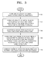
- FIG. 3 is a flowchart illustrating a method of fabricating a gas sensor according to an embodiment of the present invention. Specifically, the method of fabricating a gas sensor will now be described with reference to FIGS. 1, 2 , and 3 .
- each zinc oxide nano-structure 14 is formed on a substrate 12, for example, on a silicon substrate, using a general method. As described with reference to FIG. 1 , each zinc oxide nano-structure 14 may have a structure including a nano-wire or nano-rod.
- a plurality of metal islands 16 are formed on the surface of each zinc oxide nano-structure 14 using a solution in which a metal material is solved.
- the plurality of metal islands 16 are obtained by coating the solution in which the metal material is solved on each zinc oxide nano-structure 14.
- the metal islands 16 are separated from one another on the surface of each zinc oxide nano-structure 14.
- the solution in which the metal material is solved may be prepared as below.
- the metal material to be coated on each zinc oxide nano-structure 14 is solved in aqua regia.
- the aqua regia may be kept at a temperature in the range of about 50-100°C.
- the metal material may be a metal powder.
- the concentration of metal in the solution may be controlled to be from about 1-70 wt% based on a total weight of the solution.
- the aqua regia in which the metal is solved can be diluted so as to control the concentration of the metal in the solution to a desired value.
- distilled water or a basic solution, for example, ammonia water may be added to the aqua regia in which the metal is solved.
- a substrate 12 on which the zinc oxide nano-structures 14 are formed is dipped in the solution in which the metal having a desired concentration is solved. While the metal islands 16 are formed on the zinc oxide nano-structures 14, the solution is kept in the temperature range of about 30-100 °C.
- the zinc oxide nano-structures 14 may be dipped in the solution for a predetermined time, for example, for about one second to one minute, so as to form the metal islands 16 on the zinc oxide nano-structures 14.
- the size of the metal islands 16 formed may depend on the amount of time the zinc oxide nano-structures 14 are dipped or the concentration of the metal in the solution. Thus, a dipping time and the concentration of the metal in the solution need to be properly controlled so as to obtain the metal islands 16 having a proper size.
- water is evaporated from the surface of the zinc oxide nano-structures 14 in which the metal islands 16 are formed.
- the zinc oxide nano-structures 14 are kept from room temperature to 100 °C, preferably, from about 30-60 °C for about 1-30 minutes until water is completely evaporated from the surface of the zinc oxide nano-structures 14 after the zinc oxide nano-structures 14 in which the metal islands 16 are formed are taken out from the solution.
- a first electrode 22 is formed to be electrically connected to ends of the zinc oxide nano-structures 14 and a second electrode 24 is formed to be electrically connected to the other ends of the zinc oxide nano-structures 14.
- a current variation-measuring unit 50 is electrically connected to the first electrode 22 and the second electrode 24.
- a plurality of metal islands are formed on a plurality of zinc oxide nano-structures and the islands are formed separated from one another on the zinc oxide nano-structures.
- sensitivity to a gas is improved by the metal islands such that a gas to be detected can be detected with high sensitivity.
- gases can be detected. Gases can be detected at comparatively high detecting temperatures.
- a wet method is used to form the metal islands on the surface of the zinc oxide nano-structures.
- expensive equipment or subsequent thermal processing which has been required in a conventional method can be omitted, and the metal islands can be formed on the surface of the zinc oxide nano-structures simply, at low cost, and effectively.
- a high-sensitivity gas sensor can be fabricated at low cost using a simpler fabrication process.
Landscapes
- Chemical & Material Sciences (AREA)
- Chemical Kinetics & Catalysis (AREA)
- Electrochemistry (AREA)
- Physics & Mathematics (AREA)
- Health & Medical Sciences (AREA)
- Life Sciences & Earth Sciences (AREA)
- Analytical Chemistry (AREA)
- Biochemistry (AREA)
- General Health & Medical Sciences (AREA)
- General Physics & Mathematics (AREA)
- Immunology (AREA)
- Pathology (AREA)
- Investigating Or Analyzing Materials By The Use Of Fluid Adsorption Or Reactions (AREA)
Claims (11)
- Procédé de fabrication d'un capteur de gaz, le procédé comprenant : la formation d'une pluralité d'îlots métalliques séparés les uns des autres sur une surface de chacune d'une pluralité de nanostructures d'oxyde de zinc en revêtant des composants métalliques d'un matériau métallique sur la surface de chaque nanostructure d'oxyde de zinc dans une solution dans laquelle le matériau métallique est dissous ; et la formation d'une première électrode devant être électriquement connectée à des extrémités des nanostructures d'oxyde de zinc et une seconde électrode devant être électriquement connectée aux autres extrémités des nanostructures d'oxyde de zinc.
- Procédé selon la revendication 1, comprenant en outre, avant la formation de la première électrode et de la seconde électrode, l'évaporation de l'eau de la surface des nanostructures d'oxyde de zinc dans lesquelles les îlots métalliques sont formés.
- Procédé selon la revendication 1, dans lequel la solution comprend le matériau métallique dissous dans de l'eau régale.
- Procédé selon la revendication 3, dans lequel la solution comprend en outre au moins un élément choisi parmi l'eau distillée et une solution basique.
- Procédé selon la revendication 1, dans lequel le matériau métallique est une poudre métallique.
- Procédé selon la revendication 1, dans lequel le matériau métallique est un composé organique métallique.
- Procédé selon la revendication. 5, dans lequel le matériau métallique est formé d'un composé organique métallique choisi dans le groupe consistant en H2PtCl6, MeCpPtMe3, Pt(acac)2, Pd2(allyl)2Cl2, et Pd(C3H5) (C5H5) où Me = méthyle, Cp = cyclopentadiényl, acac = acétyl-acétone.
- Procédé selon la revendication 1, dans lequel la solution est maintenue dans une plage de température de 30 à 100 °C pendant que la pluralité d'îlots métalliques se forme.
- Procédé selon la revendication 1, dans lequel une concentration de métal dans la solution est de 1 à 70 % en poids par rapport à un poids total de la solution.
- Procédé selon la revendication 1, dans lequel les nanostructures d'oxyde de zinc sont plongées dans la solution pendant une période de temps dans la plage d'une seconde à une minute de façon à former la pluralité d'ilots métalliques.
- Procédé selon la revendication 1, comprenant en outre, avant la formation de la pluralité d'îlots métalliques, la formation des nanostructures d'oxyde de zinc sur un substrat, dans lequel la formation de la pluralité d'îlots métalliques comprend le fait de plonger le substrat sur lequel les nanostructures d'oxyde de zinc sont formées dans la solution.
Applications Claiming Priority (2)
| Application Number | Priority Date | Filing Date | Title |
|---|---|---|---|
| KR1020060067095A KR100779090B1 (ko) | 2006-07-18 | 2006-07-18 | 아연 산화물을 이용하는 가스 감지기 및 그 제조 방법 |
| PCT/KR2007/001619 WO2008010638A1 (fr) | 2006-07-18 | 2007-04-03 | Détecteur de gaz présentant des nanostructures d'oxyde de zinc et procédé pour le fabriquer |
Publications (3)
| Publication Number | Publication Date |
|---|---|
| EP2044424A1 EP2044424A1 (fr) | 2009-04-08 |
| EP2044424A4 EP2044424A4 (fr) | 2011-12-14 |
| EP2044424B1 true EP2044424B1 (fr) | 2013-02-27 |
Family
ID=38956949
Family Applications (1)
| Application Number | Title | Priority Date | Filing Date |
|---|---|---|---|
| EP07745782A Not-in-force EP2044424B1 (fr) | 2006-07-18 | 2007-04-03 | Procédé pour fabriquer un détecteur de gaz présentant des nanostructures d'oxyde de zinc |
Country Status (4)
| Country | Link |
|---|---|
| US (1) | US8087151B2 (fr) |
| EP (1) | EP2044424B1 (fr) |
| KR (1) | KR100779090B1 (fr) |
| WO (1) | WO2008010638A1 (fr) |
Families Citing this family (27)
| Publication number | Priority date | Publication date | Assignee | Title |
|---|---|---|---|---|
| KR100779090B1 (ko) | 2006-07-18 | 2007-11-27 | 한국전자통신연구원 | 아연 산화물을 이용하는 가스 감지기 및 그 제조 방법 |
| JP4122043B1 (ja) * | 2007-04-25 | 2008-07-23 | 株式会社クレステック | 面放出型電子源および描画装置 |
| US7759150B2 (en) * | 2007-05-22 | 2010-07-20 | Sharp Laboratories Of America, Inc. | Nanorod sensor with single-plane electrodes |
| CN101271078B (zh) * | 2008-04-03 | 2010-12-15 | 东南大学 | 一种生物化学传感器的制备方法 |
| KR20100035380A (ko) | 2008-09-26 | 2010-04-05 | 삼성전자주식회사 | 박막형 센싱부재를 이용한 화학 센서 |
| KR101027074B1 (ko) * | 2008-10-23 | 2011-04-05 | 서울대학교산학협력단 | 금속산화물층을 갖는 나노구조물 가스센서, 나노구조물 가스센서 어레이 및 그 제조 방법 |
| KR101538068B1 (ko) | 2009-02-02 | 2015-07-21 | 삼성전자주식회사 | 열전소자 및 그 제조방법 |
| US8742775B2 (en) * | 2009-07-17 | 2014-06-03 | Caterpillar Inc. | Zinc oxide sulfur sensor |
| KR101283685B1 (ko) * | 2009-11-23 | 2013-07-08 | 한국전자통신연구원 | 환경가스 센서 및 그의 제조방법 |
| TW201142277A (en) * | 2010-05-26 | 2011-12-01 | Univ Nat Cheng Kung | Gas sensor with a zinc-oxide nanostructure and method for producing the same |
| CN101866975B (zh) * | 2010-05-29 | 2012-05-23 | 兰州大学 | 一种半导体传感器及制备方法 |
| US8638111B2 (en) | 2010-06-17 | 2014-01-28 | Caterpillar Inc. | Zinc oxide sulfur sensor measurement system |
| US9212055B2 (en) * | 2010-09-29 | 2015-12-15 | Weilie Zhou | Aligned, coated nanowire arrays for gas sensing |
| US20120237968A1 (en) * | 2011-03-14 | 2012-09-20 | Anastasia Rigas | Detector and Method for Detection of H. Pylori |
| WO2013064157A1 (fr) * | 2011-11-04 | 2013-05-10 | Danmarks Tekniske Universitet | Détecteur de particules d'aérosol à base de fibres résonantes et procédé |
| WO2013109840A1 (fr) * | 2012-01-20 | 2013-07-25 | Caterpillar Inc. | Système de mesure de détecteur de soufre à base d'oxyde de zinc |
| EP3145403A4 (fr) | 2012-03-14 | 2018-01-24 | Anastasia Rigas | Analyseur d'haleine et procédés de test d'haleine |
| KR101358245B1 (ko) * | 2012-03-19 | 2014-02-07 | 연세대학교 산학협력단 | 수소 센서 및 수소 센서 제조 방법 |
| FR2995691B1 (fr) * | 2012-09-19 | 2014-10-10 | Commissariat Energie Atomique | Capteur de flux thermique, capteur de gaz comportant au moins un tel capteur et jauge pirani comportant au moins un tel capteur |
| US9123638B2 (en) * | 2013-03-15 | 2015-09-01 | Rohm And Haas Electronic Materials, Llc | Multi-heterojunction nanoparticles, methods of manufacture thereof and articles comprising the same |
| CN103439024A (zh) * | 2013-09-04 | 2013-12-11 | 浙江工商大学 | 纳米氧化锌温度传感器及其制备工艺 |
| CN103837583B (zh) * | 2013-11-13 | 2017-03-08 | 电子科技大学 | 一种双向生长型碳纳米管阵列传感器及其制备方法 |
| US10793964B2 (en) | 2016-05-04 | 2020-10-06 | Uchicago Argonne, Llc | Pre-treated functionalized multi-walled carbon nanotube based methane sensor |
| US11027604B2 (en) * | 2016-12-15 | 2021-06-08 | Panasonic Semiconductor Solutions Co., Ltd. | Hydrogen detection apparatus, fuel cell vehicle, hydrogen leak monitoring system, compound sensor module, hydrogen detection method, and recording medium |
| CN107589153A (zh) * | 2017-10-23 | 2018-01-16 | 京东方科技集团股份有限公司 | 气敏传感器及其制造方法、检测设备 |
| US11525818B2 (en) | 2018-01-05 | 2022-12-13 | King Fahd University Of Petroleum And Minerals | Hydrogen gas sensor and a method of fabricating thereof |
| KR102063258B1 (ko) * | 2018-05-25 | 2020-01-07 | 울산과학기술원 | 실레인 결합층을 가지는 나노 구조체 전극을 포함하는 센서 |
Family Cites Families (28)
| Publication number | Priority date | Publication date | Assignee | Title |
|---|---|---|---|---|
| US5149596A (en) * | 1990-10-05 | 1992-09-22 | The United States Of America As Represented By The United States Department Of Energy | Vapor deposition of thin films |
| US20070066480A1 (en) * | 1999-10-25 | 2007-03-22 | Moser William R | Method of preparing compounds using cavitation and compounds formed therefrom |
| MXPA03008935A (es) * | 2001-03-30 | 2004-06-30 | Univ California | Metodos de fabricacion de nanoestructuras y nanocables y dispositivos fabricados a partir de ellos. |
| US7186381B2 (en) * | 2001-07-20 | 2007-03-06 | Regents Of The University Of California | Hydrogen gas sensor |
| US7287412B2 (en) * | 2003-06-03 | 2007-10-30 | Nano-Proprietary, Inc. | Method and apparatus for sensing hydrogen gas |
| US7237429B2 (en) * | 2002-08-30 | 2007-07-03 | Nano-Proprietary, Inc. | Continuous-range hydrogen sensors |
| US6849911B2 (en) * | 2002-08-30 | 2005-02-01 | Nano-Proprietary, Inc. | Formation of metal nanowires for use as variable-range hydrogen sensors |
| US7378347B2 (en) * | 2002-10-28 | 2008-05-27 | Hewlett-Packard Development Company, L.P. | Method of forming catalyst nanoparticles for nanowire growth and other applications |
| US7608147B2 (en) * | 2003-04-04 | 2009-10-27 | Qunano Ab | Precisely positioned nanowhiskers and nanowhisker arrays and method for preparing them |
| US7265037B2 (en) * | 2003-06-20 | 2007-09-04 | The Regents Of The University Of California | Nanowire array and nanowire solar cells and methods for forming the same |
| US7545010B2 (en) * | 2003-08-08 | 2009-06-09 | Canon Kabushiki Kaisha | Catalytic sensor structure |
| US20050069457A1 (en) | 2003-09-30 | 2005-03-31 | Hon Hai Precision Industry Co., Ltd. | Gas sensor with zinc oxide layer and method for forming the same |
| US7521252B2 (en) * | 2004-02-04 | 2009-04-21 | The Research Foundation Of State University Of New York | Methods for forming palladium alloy thin films and optical hydrogen sensors employing palladium alloy thin films |
| US7354850B2 (en) * | 2004-02-06 | 2008-04-08 | Qunano Ab | Directionally controlled growth of nanowhiskers |
| US7276389B2 (en) * | 2004-02-25 | 2007-10-02 | Samsung Electronics Co., Ltd. | Article comprising metal oxide nanostructures and method for fabricating such nanostructures |
| KR100655640B1 (ko) | 2004-05-12 | 2006-12-11 | 한국과학기술연구원 | 고밀도 나노와이어 수소센서 및 그 제조방법 |
| KR100616733B1 (ko) * | 2004-07-26 | 2006-08-28 | 한국표준과학연구원 | 산화 아연계 나노 구조체 및 그의 제조 방법 |
| US7199029B2 (en) * | 2004-10-01 | 2007-04-03 | Sharp Laboratories Of America, Inc. | Selective deposition of ZnO nanostructures on a silicon substrate using a nickel catalyst and either patterned polysilicon or silicon surface modification |
| US20060102494A1 (en) | 2004-11-17 | 2006-05-18 | Industrial Technology Research Institute | Gas sensor with nanowires of zinc oxide or indium/zinc mixed oxides and method of detecting NOx gas |
| US7235475B2 (en) * | 2004-12-23 | 2007-06-26 | Hewlett-Packard Development Company, L.P. | Semiconductor nanowire fluid sensor and method for fabricating the same |
| WO2006116752A2 (fr) * | 2005-04-28 | 2006-11-02 | The Regents Of The University Of California | Compositions comprenant des nanostructures destinées à la croissance de cellules, de tissus et d'organes artificiels, procédés de préparation et d'utilisation de ces dernières |
| US7402531B1 (en) * | 2005-12-09 | 2008-07-22 | Hewlett-Packard Development Company, L.P. | Method for selectively controlling lengths of nanowires |
| US7570355B2 (en) * | 2006-01-27 | 2009-08-04 | Hewlett-Packard Development Company, L.P. | Nanowire heterostructures and methods of forming the same |
| KR100779090B1 (ko) | 2006-07-18 | 2007-11-27 | 한국전자통신연구원 | 아연 산화물을 이용하는 가스 감지기 및 그 제조 방법 |
| US8093474B2 (en) * | 2007-03-23 | 2012-01-10 | Lawrence Livermore National Security, Llc | Metallic nanospheres embedded in nanowires initiated on nanostructures and methods for synthesis thereof |
| KR100932931B1 (ko) * | 2007-07-30 | 2009-12-21 | 삼성에스디아이 주식회사 | 전자 방출원, 전자 방출 소자 및 전자 방출원의 제조 방법 |
| US8294141B2 (en) * | 2008-07-07 | 2012-10-23 | Georgia Tech Research Corporation | Super sensitive UV detector using polymer functionalized nanobelts |
| US20100108132A1 (en) * | 2008-10-30 | 2010-05-06 | General Electric Company | Nano-devices and methods of manufacture thereof |
-
2006
- 2006-07-18 KR KR1020060067095A patent/KR100779090B1/ko active IP Right Grant
-
2007
- 2007-04-03 EP EP07745782A patent/EP2044424B1/fr not_active Not-in-force
- 2007-04-03 WO PCT/KR2007/001619 patent/WO2008010638A1/fr active Application Filing
- 2007-04-03 US US12/373,908 patent/US8087151B2/en not_active Expired - Fee Related
Also Published As
| Publication number | Publication date |
|---|---|
| WO2008010638A1 (fr) | 2008-01-24 |
| EP2044424A1 (fr) | 2009-04-08 |
| US8087151B2 (en) | 2012-01-03 |
| US20100012919A1 (en) | 2010-01-21 |
| EP2044424A4 (fr) | 2011-12-14 |
| KR100779090B1 (ko) | 2007-11-27 |
Similar Documents
| Publication | Publication Date | Title |
|---|---|---|
| EP2044424B1 (fr) | Procédé pour fabriquer un détecteur de gaz présentant des nanostructures d'oxyde de zinc | |
| Urasinska-Wojcik et al. | Ultrasensitive WO3 gas sensors for NO2 detection in air and low oxygen environment | |
| US6946197B2 (en) | Semiconductor and device nanotechnology and methods for their manufacture | |
| Kim et al. | Low temperature Pd/SnO2 sensor for carbon monoxide detection | |
| EP1591777B1 (fr) | Capteur d'hydrogène et procédé de détection d'hydrogène | |
| Wang et al. | Detection of hydrogen at room temperature with catalyst-coated multiple ZnO nanorods | |
| Aroutiounian | Hydrogen detectors | |
| Dobrokhotov et al. | Toward the nanospring-based artificial olfactory system for trace-detection of flammable and explosive vapors | |
| JP2002535651A (ja) | 微細加工薄膜水素ガスセンサーおよびその製造方法および使用方法 | |
| Zhao et al. | Tin oxide thin films prepared by aerosol-assisted chemical vapor deposition and the characteristics on gas detection | |
| Traversa | Design of ceramic materials for chemical sensors with novel properties | |
| EP3786627B1 (fr) | Élément de détection de gaz à semi-conducteur de type mems | |
| WO2008153593A1 (fr) | Détecteur de gaz à base de nanomatériau | |
| Wang et al. | Room-Temperature Chemiresistive Effect of ${\rm TiO} _ {2}\!-\!{\rm B} $ Nanowires to Nitroaromatic and Nitroamine Explosives | |
| WO2002039103A9 (fr) | Detecteur d'hydrogene a hydrure metallique en film mince | |
| Stuckert et al. | The effect of Ar/O2 and H2O plasma treatment of SnO2 nanoparticles and nanowires on carbon monoxide and benzene detection | |
| Urasinska-Wojcik et al. | H 2 S sensing in dry and humid H 2 environment with p-type CuO thick-film gas sensors | |
| Laminack et al. | Dynamic interaction of NO2 with a nanostructure modified porous silicon matrix: Acidity, sensor response, and the competition for donor level electrons | |
| CN103698365B (zh) | 一种气敏传感器制备方法 | |
| WO2017132667A1 (fr) | Croissance localisée in situ de pellicules poreuses d'oxyde de métal sur une plateforme de microréchauffeur pour la détection de gaz à basse température | |
| Dutronc et al. | Influence of the nature of the screen-printed electrode metal on the transport and detection properties of thick-film semiconductor gas sensors | |
| Aroutiounian et al. | Study of hydrogen peroxide vapors sensor made of nanostructured co-doped SnO2 film | |
| White et al. | Investigation of La2CuO4∕ YSZ∕ Pt Potentiometric NO x Sensors with Electrochemical Impedance Spectroscopy | |
| CN113544499A (zh) | 电阻式金属氧化物气体传感器及其制造方法和操作该传感器的方法 | |
| Aroutiounian | Use of metaloxide, porous silicon and carbon nanotube gas sensors for safety and security |
Legal Events
| Date | Code | Title | Description |
|---|---|---|---|
| PUAI | Public reference made under article 153(3) epc to a published international application that has entered the european phase |
Free format text: ORIGINAL CODE: 0009012 |
|
| 17P | Request for examination filed |
Effective date: 20090218 |
|
| AK | Designated contracting states |
Kind code of ref document: A1 Designated state(s): AT BE BG CH CY CZ DE DK EE ES FI FR GB GR HU IE IS IT LI LT LU LV MC MT NL PL PT RO SE SI SK TR |
|
| AX | Request for extension of the european patent |
Extension state: AL BA HR MK RS |
|
| RIC1 | Information provided on ipc code assigned before grant |
Ipc: G01N 27/12 20060101AFI20111020BHEP |
|
| A4 | Supplementary search report drawn up and despatched |
Effective date: 20111114 |
|
| RIC1 | Information provided on ipc code assigned before grant |
Ipc: G01N 27/12 20060101AFI20111104BHEP |
|
| DAX | Request for extension of the european patent (deleted) | ||
| GRAP | Despatch of communication of intention to grant a patent |
Free format text: ORIGINAL CODE: EPIDOSNIGR1 |
|
| GRAS | Grant fee paid |
Free format text: ORIGINAL CODE: EPIDOSNIGR3 |
|
| GRAA | (expected) grant |
Free format text: ORIGINAL CODE: 0009210 |
|
| AK | Designated contracting states |
Kind code of ref document: B1 Designated state(s): AT BE BG CH CY CZ DE DK EE ES FI FR GB GR HU IE IS IT LI LT LU LV MC MT NL PL PT RO SE SI SK TR |
|
| REG | Reference to a national code |
Ref country code: GB Ref legal event code: FG4D |
|
| REG | Reference to a national code |
Ref country code: CH Ref legal event code: EP |
|
| REG | Reference to a national code |
Ref country code: AT Ref legal event code: REF Ref document number: 598750 Country of ref document: AT Kind code of ref document: T Effective date: 20130315 |
|
| REG | Reference to a national code |
Ref country code: IE Ref legal event code: FG4D |
|
| REG | Reference to a national code |
Ref country code: DE Ref legal event code: R096 Ref document number: 602007028718 Country of ref document: DE Effective date: 20130425 |
|
| REG | Reference to a national code |
Ref country code: AT Ref legal event code: MK05 Ref document number: 598750 Country of ref document: AT Kind code of ref document: T Effective date: 20130227 |
|
| REG | Reference to a national code |
Ref country code: LT Ref legal event code: MG4D |
|
| PG25 | Lapsed in a contracting state [announced via postgrant information from national office to epo] |
Ref country code: BG Free format text: LAPSE BECAUSE OF FAILURE TO SUBMIT A TRANSLATION OF THE DESCRIPTION OR TO PAY THE FEE WITHIN THE PRESCRIBED TIME-LIMIT Effective date: 20130527 Ref country code: ES Free format text: LAPSE BECAUSE OF FAILURE TO SUBMIT A TRANSLATION OF THE DESCRIPTION OR TO PAY THE FEE WITHIN THE PRESCRIBED TIME-LIMIT Effective date: 20130607 Ref country code: AT Free format text: LAPSE BECAUSE OF FAILURE TO SUBMIT A TRANSLATION OF THE DESCRIPTION OR TO PAY THE FEE WITHIN THE PRESCRIBED TIME-LIMIT Effective date: 20130227 Ref country code: LT Free format text: LAPSE BECAUSE OF FAILURE TO SUBMIT A TRANSLATION OF THE DESCRIPTION OR TO PAY THE FEE WITHIN THE PRESCRIBED TIME-LIMIT Effective date: 20130227 Ref country code: IS Free format text: LAPSE BECAUSE OF FAILURE TO SUBMIT A TRANSLATION OF THE DESCRIPTION OR TO PAY THE FEE WITHIN THE PRESCRIBED TIME-LIMIT Effective date: 20130627 Ref country code: SE Free format text: LAPSE BECAUSE OF FAILURE TO SUBMIT A TRANSLATION OF THE DESCRIPTION OR TO PAY THE FEE WITHIN THE PRESCRIBED TIME-LIMIT Effective date: 20130227 |
|
| REG | Reference to a national code |
Ref country code: NL Ref legal event code: VDEP Effective date: 20130227 |
|
| PG25 | Lapsed in a contracting state [announced via postgrant information from national office to epo] |
Ref country code: FI Free format text: LAPSE BECAUSE OF FAILURE TO SUBMIT A TRANSLATION OF THE DESCRIPTION OR TO PAY THE FEE WITHIN THE PRESCRIBED TIME-LIMIT Effective date: 20130227 Ref country code: PL Free format text: LAPSE BECAUSE OF FAILURE TO SUBMIT A TRANSLATION OF THE DESCRIPTION OR TO PAY THE FEE WITHIN THE PRESCRIBED TIME-LIMIT Effective date: 20130227 Ref country code: LV Free format text: LAPSE BECAUSE OF FAILURE TO SUBMIT A TRANSLATION OF THE DESCRIPTION OR TO PAY THE FEE WITHIN THE PRESCRIBED TIME-LIMIT Effective date: 20130227 Ref country code: GR Free format text: LAPSE BECAUSE OF FAILURE TO SUBMIT A TRANSLATION OF THE DESCRIPTION OR TO PAY THE FEE WITHIN THE PRESCRIBED TIME-LIMIT Effective date: 20130528 Ref country code: BE Free format text: LAPSE BECAUSE OF FAILURE TO SUBMIT A TRANSLATION OF THE DESCRIPTION OR TO PAY THE FEE WITHIN THE PRESCRIBED TIME-LIMIT Effective date: 20130227 Ref country code: SI Free format text: LAPSE BECAUSE OF FAILURE TO SUBMIT A TRANSLATION OF THE DESCRIPTION OR TO PAY THE FEE WITHIN THE PRESCRIBED TIME-LIMIT Effective date: 20130227 Ref country code: PT Free format text: LAPSE BECAUSE OF FAILURE TO SUBMIT A TRANSLATION OF THE DESCRIPTION OR TO PAY THE FEE WITHIN THE PRESCRIBED TIME-LIMIT Effective date: 20130627 |
|
| PG25 | Lapsed in a contracting state [announced via postgrant information from national office to epo] |
Ref country code: NL Free format text: LAPSE BECAUSE OF FAILURE TO SUBMIT A TRANSLATION OF THE DESCRIPTION OR TO PAY THE FEE WITHIN THE PRESCRIBED TIME-LIMIT Effective date: 20130227 Ref country code: RO Free format text: LAPSE BECAUSE OF FAILURE TO SUBMIT A TRANSLATION OF THE DESCRIPTION OR TO PAY THE FEE WITHIN THE PRESCRIBED TIME-LIMIT Effective date: 20130227 Ref country code: EE Free format text: LAPSE BECAUSE OF FAILURE TO SUBMIT A TRANSLATION OF THE DESCRIPTION OR TO PAY THE FEE WITHIN THE PRESCRIBED TIME-LIMIT Effective date: 20130227 Ref country code: DK Free format text: LAPSE BECAUSE OF FAILURE TO SUBMIT A TRANSLATION OF THE DESCRIPTION OR TO PAY THE FEE WITHIN THE PRESCRIBED TIME-LIMIT Effective date: 20130227 Ref country code: CZ Free format text: LAPSE BECAUSE OF FAILURE TO SUBMIT A TRANSLATION OF THE DESCRIPTION OR TO PAY THE FEE WITHIN THE PRESCRIBED TIME-LIMIT Effective date: 20130227 Ref country code: SK Free format text: LAPSE BECAUSE OF FAILURE TO SUBMIT A TRANSLATION OF THE DESCRIPTION OR TO PAY THE FEE WITHIN THE PRESCRIBED TIME-LIMIT Effective date: 20130227 |
|
| PG25 | Lapsed in a contracting state [announced via postgrant information from national office to epo] |
Ref country code: CY Free format text: LAPSE BECAUSE OF FAILURE TO SUBMIT A TRANSLATION OF THE DESCRIPTION OR TO PAY THE FEE WITHIN THE PRESCRIBED TIME-LIMIT Effective date: 20130227 Ref country code: MC Free format text: LAPSE BECAUSE OF FAILURE TO SUBMIT A TRANSLATION OF THE DESCRIPTION OR TO PAY THE FEE WITHIN THE PRESCRIBED TIME-LIMIT Effective date: 20130227 |
|
| REG | Reference to a national code |
Ref country code: CH Ref legal event code: PL |
|
| PG25 | Lapsed in a contracting state [announced via postgrant information from national office to epo] |
Ref country code: IT Free format text: LAPSE BECAUSE OF FAILURE TO SUBMIT A TRANSLATION OF THE DESCRIPTION OR TO PAY THE FEE WITHIN THE PRESCRIBED TIME-LIMIT Effective date: 20130227 |
|
| PLBE | No opposition filed within time limit |
Free format text: ORIGINAL CODE: 0009261 |
|
| STAA | Information on the status of an ep patent application or granted ep patent |
Free format text: STATUS: NO OPPOSITION FILED WITHIN TIME LIMIT |
|
| GBPC | Gb: european patent ceased through non-payment of renewal fee |
Effective date: 20130527 |
|
| REG | Reference to a national code |
Ref country code: IE Ref legal event code: MM4A |
|
| PG25 | Lapsed in a contracting state [announced via postgrant information from national office to epo] |
Ref country code: CH Free format text: LAPSE BECAUSE OF NON-PAYMENT OF DUE FEES Effective date: 20130430 Ref country code: LI Free format text: LAPSE BECAUSE OF NON-PAYMENT OF DUE FEES Effective date: 20130430 |
|
| REG | Reference to a national code |
Ref country code: FR Ref legal event code: ST Effective date: 20131231 |
|
| 26N | No opposition filed |
Effective date: 20131128 |
|
| PG25 | Lapsed in a contracting state [announced via postgrant information from national office to epo] |
Ref country code: FR Free format text: LAPSE BECAUSE OF NON-PAYMENT OF DUE FEES Effective date: 20130430 |
|
| REG | Reference to a national code |
Ref country code: DE Ref legal event code: R097 Ref document number: 602007028718 Country of ref document: DE Effective date: 20131128 |
|
| PG25 | Lapsed in a contracting state [announced via postgrant information from national office to epo] |
Ref country code: IE Free format text: LAPSE BECAUSE OF NON-PAYMENT OF DUE FEES Effective date: 20130403 Ref country code: GB Free format text: LAPSE BECAUSE OF NON-PAYMENT OF DUE FEES Effective date: 20130527 |
|
| PGFP | Annual fee paid to national office [announced via postgrant information from national office to epo] |
Ref country code: DE Payment date: 20140327 Year of fee payment: 8 |
|
| PG25 | Lapsed in a contracting state [announced via postgrant information from national office to epo] |
Ref country code: MT Free format text: LAPSE BECAUSE OF FAILURE TO SUBMIT A TRANSLATION OF THE DESCRIPTION OR TO PAY THE FEE WITHIN THE PRESCRIBED TIME-LIMIT Effective date: 20130227 |
|
| PG25 | Lapsed in a contracting state [announced via postgrant information from national office to epo] |
Ref country code: TR Free format text: LAPSE BECAUSE OF FAILURE TO SUBMIT A TRANSLATION OF THE DESCRIPTION OR TO PAY THE FEE WITHIN THE PRESCRIBED TIME-LIMIT Effective date: 20130227 |
|
| PG25 | Lapsed in a contracting state [announced via postgrant information from national office to epo] |
Ref country code: HU Free format text: LAPSE BECAUSE OF FAILURE TO SUBMIT A TRANSLATION OF THE DESCRIPTION OR TO PAY THE FEE WITHIN THE PRESCRIBED TIME-LIMIT; INVALID AB INITIO Effective date: 20070403 Ref country code: LU Free format text: LAPSE BECAUSE OF NON-PAYMENT OF DUE FEES Effective date: 20130403 |
|
| REG | Reference to a national code |
Ref country code: DE Ref legal event code: R119 Ref document number: 602007028718 Country of ref document: DE |
|
| PG25 | Lapsed in a contracting state [announced via postgrant information from national office to epo] |
Ref country code: DE Free format text: LAPSE BECAUSE OF NON-PAYMENT OF DUE FEES Effective date: 20151103 |