EP2043155A2 - AC-Lichtemittierende Diode - Google Patents
AC-Lichtemittierende Diode Download PDFInfo
- Publication number
- EP2043155A2 EP2043155A2 EP08012492A EP08012492A EP2043155A2 EP 2043155 A2 EP2043155 A2 EP 2043155A2 EP 08012492 A EP08012492 A EP 08012492A EP 08012492 A EP08012492 A EP 08012492A EP 2043155 A2 EP2043155 A2 EP 2043155A2
- Authority
- EP
- European Patent Office
- Prior art keywords
- light emitting
- emitting cells
- led
- substrate
- wires
- Prior art date
- Legal status (The legal status is an assumption and is not a legal conclusion. Google has not performed a legal analysis and makes no representation as to the accuracy of the status listed.)
- Granted
Links
Images


Classifications
-
- H—ELECTRICITY
- H10—SEMICONDUCTOR DEVICES; ELECTRIC SOLID-STATE DEVICES NOT OTHERWISE PROVIDED FOR
- H10H—INORGANIC LIGHT-EMITTING SEMICONDUCTOR DEVICES HAVING POTENTIAL BARRIERS
- H10H29/00—Integrated devices, or assemblies of multiple devices, comprising at least one light-emitting semiconductor element covered by group H10H20/00
- H10H29/10—Integrated devices comprising at least one light-emitting semiconductor component covered by group H10H20/00
- H10H29/14—Integrated devices comprising at least one light-emitting semiconductor component covered by group H10H20/00 comprising multiple light-emitting semiconductor components
- H10H29/142—Two-dimensional arrangements, e.g. asymmetric LED layout
-
- H—ELECTRICITY
- H10—SEMICONDUCTOR DEVICES; ELECTRIC SOLID-STATE DEVICES NOT OTHERWISE PROVIDED FOR
- H10H—INORGANIC LIGHT-EMITTING SEMICONDUCTOR DEVICES HAVING POTENTIAL BARRIERS
- H10H20/00—Individual inorganic light-emitting semiconductor devices having potential barriers, e.g. light-emitting diodes [LED]
- H10H20/80—Constructional details
- H10H20/81—Bodies
- H10H20/817—Bodies characterised by the crystal structures or orientations, e.g. polycrystalline, amorphous or porous
-
- H—ELECTRICITY
- H10—SEMICONDUCTOR DEVICES; ELECTRIC SOLID-STATE DEVICES NOT OTHERWISE PROVIDED FOR
- H10H—INORGANIC LIGHT-EMITTING SEMICONDUCTOR DEVICES HAVING POTENTIAL BARRIERS
- H10H20/00—Individual inorganic light-emitting semiconductor devices having potential barriers, e.g. light-emitting diodes [LED]
- H10H20/80—Constructional details
- H10H20/81—Bodies
- H10H20/822—Materials of the light-emitting regions
- H10H20/824—Materials of the light-emitting regions comprising only Group III-V materials, e.g. GaP
- H10H20/825—Materials of the light-emitting regions comprising only Group III-V materials, e.g. GaP containing nitrogen, e.g. GaN
-
- H—ELECTRICITY
- H10—SEMICONDUCTOR DEVICES; ELECTRIC SOLID-STATE DEVICES NOT OTHERWISE PROVIDED FOR
- H10H—INORGANIC LIGHT-EMITTING SEMICONDUCTOR DEVICES HAVING POTENTIAL BARRIERS
- H10H20/00—Individual inorganic light-emitting semiconductor devices having potential barriers, e.g. light-emitting diodes [LED]
- H10H20/80—Constructional details
- H10H20/85—Packages
- H10H20/857—Interconnections, e.g. lead-frames, bond wires or solder balls
-
- H10P14/2921—
-
- H10P14/2926—
-
- H10P14/3416—
-
- H10P14/3466—
-
- H10W90/753—
Definitions
- the present invention relates to a light emitting diode operated by being directly connected to an AC power source, and more particularly, to an AC light emitting diode having improved performance such as quantum efficiency.
- a light emitting diode which is a photoelectric conversion device having a structure in which an N-type semiconductor and a P-type semiconductor are joined together, emits predetermined light through recombination of the electrons and holes.
- LED is widely used for display elements and backlights. Further, LEDs have less electric power consumption and a longer lifespan as compared with conventional light bulbs or fluorescent lamps, so that their application areas have been expanded to the use thereof for general illumination while substituting for conventional incandescent bulbs and fluorescent lamps.
- the conventional AC LED has a structure in which a plurality of light emitting cells are two-dimensionally arranged on a single substrate. Each of the light emitting cells has GaN-based semiconductor layers grown on the single substrate.
- the present inventors have proposed a technique for compensating for a light emitting amount decreased by the reduction of a light emitting region by enhancing quantum efficiency (particularly, internal quantum efficiency) in an AC LED in which the area of the light emitting region is relatively reduced due to employment of the light emitting cells.
- a c-plane ⁇ 0001 ⁇ substrate particularly a c-plane sapphire substrate is used as a single substrate on which GaN-based semiconductor layers are grown.
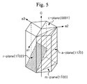
- GaN and its compounds are the most stable in a hexagonal system crystal structure expressed by axes of equivalent bases, which rotate at an angle of 120 degrees with respect to each other and are all perpendicular to the unique c-axis as shown in Fig. 5 .
- each plane contains only one kind of atom, i.e., Ga or N while advancing along the c-axis plane by plane.
- GaN crystals form the boundary between one c-plane containing only nitrogen atoms and one c-plane containing only gallium atoms.
- the GaN crystals are polarized along the c-axis, and the voluntary polarization of the GaN crystals depends on the crystal structure and composition as bulk properties.
- the conventional AC LED comprises light emitting cells consisting of GaN-based semiconductor layers grown along a c-axis direction.
- c-plane quantum well structures of the LED are influenced by a quantum-confined stark effect (QCSE) in an active region.
- QCSE quantum-confined stark effect
- electrons and holes are spatially separated by strong internal electric fields along the c-direction, so that recombination efficiency of electrons and holes is considerably deteriorated.
- an object of the present invention is to provide an AC LED, wherein a non-polar substrate is used instead of a polar substrate, which has been used as a single substrate of a conventional AC LED, whereby the quantum efficiency is enhanced, and therefore, the luminous efficiency of the AC LED having a small light emitting region per chip is increased.
- Another object of the present invention is to provide an AC LED, in which light emitting cells are arranged to secure excellent operation properties and optical power at a chip level having a limited size.
- a further object of the present invention is to provide an AC LED capable of preventing a transient voltage from being applied to a specific light emitting cell when the AC LED operates.
- the single substrate is a non-polar substrate, and the light emitting cells have non-polar GaN-based semiconductor layers grown on the non-polar substrate.
- the GaN-based semiconductor layers may be a-plane GaN-based semiconductor layers grown using an r-plane sapphire substrate or a-GaN substrate as the non-polar substrate.
- the GaN-based semiconductor layers may be m-plane GaN-based semiconductor layers grown using an m-plane sapphire substrate or m-GaN substrate as the non-polar substrate.
- non-polar substrate or “substrate” having the meaning similar thereto is defined as a substrate having an r-, m- or a-plane on which a non-polar a- or m-plane GaN-based compound is grown.
- the serial array is operated by being connected to an AC power source.
- the serial array may comprise first and second serial arrays, and the first and second serial arrays are connected in reverse parallel to be operated by AC power.
- a bridge rectifier may be formed by connecting some of the light emitting cells formed on the single substrate through wires.
- the serial array of the light emitting cells is electrically connected to the bridge rectifier, thereby being operated by the AC power source. Accordingly, there is provided an AC LED capable of being operated by being connected to an AC power source.
- the light emitting cells are laterally and longitudinally spaced apart from one another at distances, each of which is ranged from 10 to 30 ⁇ m, respectively.
- the distance between the light emitting cells becomes narrow. For this reason, contaminants such as particles remain between the light emitting cells, and therefore, current leakage may occur between the light emitting cells.
- a turned-on voltage and operation voltage of the serial array of the light emitting cells is increased, and operation time of the light emitting cells is shortened accordingly. That is, when the LED is operated under AC power, a voltage applied to the array of the light emitting cells depending on the phase of AC power is changed in the form of a sine wave. At this time, if the turned-on voltage and operation voltage of the serial array of the light emitting cells is large, the light emitting cells are turned on and operated when the applied voltage is considerably increased. In a state where the applied voltage is small, the light emitting cells are not operated.
- each of the light emitting cells comprise a non-polar first conductive semiconductor layer formed on the non-polar substrate, a non-polar second conductive semiconductor layer formed on top of one region of the first conductive semiconductor layer, and a non-polar active layer interposed between the first and second conductive semiconductor layers.
- the first conductive semiconductor layer, the active layer and the second conductive semiconductor layer may be formed of a III-V compound semiconductor, particularly (Al, In, Ga)N.
- Each of the wires electrically connects the first conductive semiconductor layer of one of the light emitting cells to the second conductive semiconductor layer of adjacent another of the light emitting cells, thereby forming the serial array of the light emitting cells.
- At least one shunt wire electrically connects corresponding wires in the first and second serial arrays connected in reverse parallel to each other.
- the shunt wire prevents an overvoltage from being applied to a specific light emitting cell in the serial array to which a reverse voltage is applied when the AC LED is operated.
- the at least shunt wire may be formed together with the wires using the same material as the wires. Further, the at least shunt wire may be disposed between the light emitting cells.
- a transparent electrode layer may be formed on the second conductive semiconductor layer of each of the light emitting cells.
- the transparent electrode layer allows current in the second conductive semiconductor layer to be uniformly spread, and allows light generated from the active layer to be emitted upward from the second conductive semiconductor layer.
- bonding patterns may be formed on the submount substrate.
- the wire may also be formed using the boning patterns formed on the submount substrate.
- Fig. 1 is a plan view illustrating an AC LED according to an embodiment of the present invention
- Fig. 2 is a sectional view taken along line A-A of Fig. 1 .
- a plurality of light emitting cells 30 are arranged on a substrate 21.
- the substrate 21 has a limited size, for example, a size of 2000x2000 ⁇ m 2 or less.
- the size of the substrate 21 means the size of a single chip, such a single chip is standardized within the aforementioned size.
- the substrate 21 is a non-polar substrate, and in this embodiment, an r-plane ⁇ 1 1 02 ⁇ (see Fig. 5 ) sapphire substrate is used as the substrate 21.
- GaN-based semiconductor layers including the first conductive semiconductor layer 25, the second conductive semiconductor layer 29 and the active layer 27 are grown on the r-plane sapphire substrate, thereby forming non-polar GaN-based semiconductor layers, particularly a-plane ⁇ 1 1 20 ⁇ (see Fig. 5 ) GaN-based semiconductor layers.
- an a-GaN substrate having the a-plane ⁇ 1 1 20 ⁇ as a growth plane may be used as the substrate.
- the a-GaN substrate may be grown on the r-plane sapphire substrate.
- an m-plane ⁇ 1 1 00 ⁇ (see Fig. 5 ) sapphire substrate or m-GaN substrate may also be used as the non-polar substrate.
- the non-polar GaN-based semiconductor layers grown on such a non-polar substrate become m-plane GaN-based semiconductor layers.
- a method for growing non-polar GaN-based semiconductor layers on an r-plane or m-plane sapphire substrate or an a-GaN or m-GaN substrate preferably include hydride vapor phase epitaxy (HVPE), metal organic chemical vapor deposition (MOCVD), molecular beam epitaxy (MBE), liquid phase epitaxy (LPE), plasma-enhanced chemical vapor deposition (PECVD), and the like.
- HVPE hydride vapor phase epitaxy
- MOCVD metal organic chemical vapor deposition
- MBE molecular beam epitaxy
- LPE liquid phase epitaxy
- PECVD plasma-enhanced chemical vapor deposition
- the non-polar GaN-based semiconductor layers obtained as described above remove an electromagnetic field induced by polarization that reduces the recombination rate of electrons and holes in an active region, so that recombination efficiency of electrons and holes in the active layer 27 are improved, thereby enhancing quantum efficiency.
- the light emitting cells 30 are electrically connected to one another by wires 37.
- Each of the wires 37 connects the first conductive semiconductor layer 25 of one of the light emitting cells to the second conductive semiconductor layer 29 of adjacent another of the light emitting cells.
- a first electrode pad 31 is formed on the first conductive semiconductor layer 25, and a transparent electrode layer 33 is formed on the second conductive semiconductor layer 29.
- the transparent electrode layer 33 may be formed of a material such as indium tin oxide (ITO) or Ni/Au.
- ITO indium tin oxide
- the transparent electrode layer 33 allows current to be uniformly spread in the second conductive semiconductor layer 29. Since the transparent electrode layer 33 has transmittance with respect to light generated in the active layer 27, the light can be emitted upward from the second conductive semiconductor layer 29.
- the insulating layer 35 may be formed by depositing a silicon oxide layer SiO 2 or a silicon nitride layer Si 3 N 4 on top of the entire surface of the substrate 21 having the light emitting cells 30, the transparent electrode layers 33, the first electrode pads 31 and the like formed thereon. The insulating layer 35 is patterned to expose the transparent electrodes 33 and the first electrode pads 31. Each of the wires 37 is formed on the insulating layer 35 to connect the exposed transparent electrode layer 33 and the first electrode pad 31.
- First and second serial arrays 11 and 13 having the light emitting cells 30 connected in series are formed by the wires 37.
- the first and second serial arrays 11 and 13 that are connected in reverse parallel are operated by an AC power source (not shown).
- the first and second serial arrays 11 and 13 are alternately operated depending on the phase of AC power, so that light is continuously emitted.
- At least one shunt wire 38 electrically connects corresponding light emitting cells in the first and second serial arrays 11 and 13.
- the shunt wire 38 allows the corresponding light emitting cells in the first and second serial arrays 11 and 13 to have the same electric potential. Accordingly, when the serial arrays 11 and 13 connected in reverse parallel under AC power are operated, the light emitting cells are protected by preventing overvoltage from being applied to a specific light emitting cell in the serial array to which a reverse voltage is applied.
- the shunt wires 38 may electrically connect most of the light emitting cells so that all the corresponding light emitting cells in the first and second serial arrays 11 and 13 have the same electric potential.
- the present invention is not limited thereto, but some light emitting cells may be connected by the shunt wires.
- pads 41 a and 41 b are formed on the substrate 21, i.e., the non-polar substrate, and the first and second serial arrays 11 and 13 may be connected in reverse parallel to the pads 41a and 41b.
- the light emitting cells are laterally and longitudinally spaced apart from one another at distances "a" and "b", each of which is ranged from 10 to 30 ⁇ m, respectively. If the light emitting cells are spaced apart from one another by a distance of 10 ⁇ m or less, it is difficult to perform an etching process for electrically isolating the light emitting cells from one another. In addition, contaminants such as particles remain between the light emitting cells, and therefore, current leakage may occur between the light emitting cells. Further, if the spacing distance between the light emitting cells is 10 ⁇ m or less, it is difficult to form the insulating layer 33 and the wires 37, and a short circuit may occur between the wires 37.
- the light emitting cells 30 are spaced apart from one another by a distance of 10 ⁇ m or more, so that the light emitting cells 30 can be easily formed using an etching technique, and the insulating layer 35, the wires 37 and the shunt wires 38 can be easily formed. In addition, it is possible to prevent leakage current between the light emitting cells.
- the light emitting cells are spaced apart from one another by a distance of over 30 ⁇ m, the turned-on voltage of the serial array is excessively increased, and the operation time of the AC LED is decreased. Therefore, the amount of light emitted from the LED is decreased, and serious flickering may occur.
- the distance between the light emitting cells is limited to 30 ⁇ m or less, whereby it is possible to reduce the flickering of the AC LED and the damage to the light emitting cells by the etching.
- first and second serial arrays 11 and 13 are operated in a state of being connected in reverse parallel.
- a single serial array with the light emitting cells connected in series may be formed on a single substrate.
- a bridge rectifier is formed on the substrate, and the serial array is connected to the bridge rectifier to be operated under AC power.
- the bridge rectifier may be formed by connecting the light emitting cells formed on the single substrate using wires.
- Fig. 3 is a sectional view illustrating an AC LED according to another embodiment of the present invention.
- a plurality of light emitting cells 30 having non-polar GaN-based semiconductor layers formed on a non-polar substrate 21 are two-dimensionally arranged as described with reference to Figs. 1 and 2 .
- a transparent electrode layer 33 may be formed on a second conductive semiconductor layer 29 of the light emitting cells 30, and first electrode pads 31 may be formed on the first conductive semiconductor layers 25.
- the light emitting cells 30 are electrically connected by wires 47 to form serial arrays.
- the wires 47 connecting the light emitting cells 30 are formed by an air bridge process, unlike the wires 37 described with reference to Fig. 2 . In each of the wires 47, a portion except its contacts is spaced apart from the substrate.
- the light emitting cells are laterally and longitudinally spaced apart from one another by distances, each of which is ranged from 10 to 30 ⁇ m as described with reference to Figs. 1 and 2 .
- a plurality of light emitting cells 30 having non-polar GaN-based semiconductor layers formed on a non-polar substrate 21 are two-dimensionally arranged as described with reference to Fig. 3 .
- metal bumps 51 and 55 are formed on top of first and second conductive semiconductor layers 25 and 29, respectively, and the light emitting cells 30 are flip-bonded on a submount substrate 61 through the metal bumps 51 and 55.
- a reflection layer 53 is formed on the second conductive semiconductor layer 29 to reflect light that is generated from an active layer 27 and directed to the submount substrate 61.
- First electrode pads 31 may be interposed between the metal bumps 51 and the first conductive semiconductor layers 25.
- bonding patterns 63 for bonding the metal bumps 51 and 55 may be formed on the submount substrate 61. Pads (not shown) for electrically connecting the LED to an AC power source may also be formed on the submount substrate 61.
- the light emitting cells are flip-bonded so that the first conductive semiconductor layer 25 of one of the light emitting cells and the second conductive semiconductor layer 29 of adjacent another of the light emitting cells are electrically bonded to one bonding pattern 63. Therefore, the light emitting cells 30 can be connected in series to one another using the bonding patterns 63. That is, the bonding patterns 63 may serve as wires for connecting the light emitting cells. Accordingly, the light emitting cells 30 are connected by the bonding patterns 63, so that first and second serial arrays (11 and 13 of Fig. 1 ) can be formed.
- the light emitting cells 30 are flip-bonded on the submount substrate 61, heat generated from the light emitting cells 30 during the operation can be dissipated through the submount substrate 61, thereby enhancing light emitting efficiency.
- the light emitting cells 30 are connected in series to one another by the bonding patterns 63, but the present invention is not limited thereto. That is, the wires 37 ( Fig. 2 ) or 47 ( Fig. 3 ) for electrically connecting the light emitting cells 30 may be separately formed, and the light emitting cells 30 may be flip-bonded to corresponding bonding patterns through the metal bumps, respectively. In this case, the metal bumps 51 formed on the first conductive semiconductor layer 25 may be omitted.
- a non-polar structure of GaN-based semiconductor layers constituting light emitting cells is employed, so that it is possible to improve the recombination efficiency of electrons and holes in an active region and accordingly to enhance the quantum efficiency. Therefore, it is possible to considerably improve a phenomenon that the amount of light emitted from an AC LED is decreased due to a small area of a light emitting region per chip.
- an AC LED which can be continuously operated by being connected to an AC power source. Further, the spacing distance between light emitting cells is set to be in a range of 10 to 30 ⁇ m, so that turned-on voltage and operation voltage can be lowered, thereby increasing light emitting time of the LED connected to the AC power source. Accordingly, the amount of light emitted from the LED can be increased, and flickering of the AC LED can be reduced.
- the light emitting cells are spaced apart from one another by a distance of 10 ⁇ m or more, so that wires for connecting the light emitting cells can be easily formed, and short circuits that occur between the wires can be prevented.
- the light emitting cells are spaced apart from one another by a distance of 30 ⁇ m or less, so that it is possible to reduce etching time for forming the light emitting cells, and therefore, prevent the light emitting cells to be damaged by the etching.
Landscapes
- Led Devices (AREA)
- Led Device Packages (AREA)
Applications Claiming Priority (1)
| Application Number | Priority Date | Filing Date | Title |
|---|---|---|---|
| KR1020070097330A KR100889956B1 (ko) | 2007-09-27 | 2007-09-27 | 교류용 발광다이오드 |
Publications (3)
| Publication Number | Publication Date |
|---|---|
| EP2043155A2 true EP2043155A2 (de) | 2009-04-01 |
| EP2043155A3 EP2043155A3 (de) | 2010-05-12 |
| EP2043155B1 EP2043155B1 (de) | 2015-09-09 |
Family
ID=40125237
Family Applications (1)
| Application Number | Title | Priority Date | Filing Date |
|---|---|---|---|
| EP08012492.8A Ceased EP2043155B1 (de) | 2007-09-27 | 2008-07-10 | AC-Lichtemittierende Diode |
Country Status (4)
| Country | Link |
|---|---|
| US (1) | US8269228B2 (de) |
| EP (1) | EP2043155B1 (de) |
| JP (1) | JP2009088482A (de) |
| KR (1) | KR100889956B1 (de) |
Families Citing this family (34)
| Publication number | Priority date | Publication date | Assignee | Title |
|---|---|---|---|---|
| KR101158073B1 (ko) * | 2005-12-13 | 2012-06-22 | 서울옵토디바이스주식회사 | 다수개의 발광 셀이 어레이된 발광 소자 |
| US8698184B2 (en) * | 2011-01-21 | 2014-04-15 | Cree, Inc. | Light emitting diodes with low junction temperature and solid state backlight components including light emitting diodes with low junction temperature |
| US9443903B2 (en) | 2006-06-30 | 2016-09-13 | Cree, Inc. | Low temperature high strength metal stack for die attachment |
| WO2008111693A1 (en) * | 2007-03-13 | 2008-09-18 | Seoul Opto Device Co., Ltd. | Ac light emitting diode |
| US8716723B2 (en) * | 2008-08-18 | 2014-05-06 | Tsmc Solid State Lighting Ltd. | Reflective layer between light-emitting diodes |
| US9293656B2 (en) * | 2012-11-02 | 2016-03-22 | Epistar Corporation | Light emitting device |
| US9117944B2 (en) * | 2008-09-24 | 2015-08-25 | Koninklijke Philips N.V. | Semiconductor light emitting devices grown on composite substrates |
| JP4486701B1 (ja) | 2008-11-06 | 2010-06-23 | パナソニック株式会社 | 窒化物系半導体素子およびその製造方法 |
| KR101017395B1 (ko) * | 2008-12-24 | 2011-02-28 | 서울옵토디바이스주식회사 | 복수개의 발광셀들을 갖는 발광 소자 및 그것을 제조하는 방법 |
| KR101557362B1 (ko) | 2008-12-31 | 2015-10-08 | 서울바이오시스 주식회사 | 복수개의 비극성 발광셀들을 갖는 발광 소자 및 그것을 제조하는 방법 |
| KR101533817B1 (ko) | 2008-12-31 | 2015-07-09 | 서울바이오시스 주식회사 | 복수개의 비극성 발광셀들을 갖는 발광 소자 및 그것을 제조하는 방법 |
| US8058639B2 (en) | 2009-04-06 | 2011-11-15 | Panasonic Corporation | Nitride semiconductor element and method for production thereof |
| TWI398966B (zh) * | 2009-06-08 | 2013-06-11 | 晶元光電股份有限公司 | 發光元件及其製造方法 |
| WO2011013709A1 (ja) * | 2009-07-31 | 2011-02-03 | Jsr株式会社 | 発光素子、発光素子の製造方法及び発光素子保護層形成用組成物 |
| US9236532B2 (en) * | 2009-12-14 | 2016-01-12 | Seoul Viosys Co., Ltd. | Light emitting diode having electrode pads |
| JP5463901B2 (ja) * | 2009-12-24 | 2014-04-09 | 日亜化学工業株式会社 | 発光装置 |
| WO2011077704A1 (ja) * | 2009-12-25 | 2011-06-30 | パナソニック株式会社 | 窒化物系半導体素子およびその製造方法 |
| CN102340904B (zh) | 2010-07-14 | 2015-06-17 | 通用电气公司 | 发光二极管驱动装置及其驱动方法 |
| US9070851B2 (en) | 2010-09-24 | 2015-06-30 | Seoul Semiconductor Co., Ltd. | Wafer-level light emitting diode package and method of fabricating the same |
| US8592847B2 (en) * | 2011-04-15 | 2013-11-26 | Epistar Corporation | Light-emitting device |
| KR101900269B1 (ko) * | 2012-01-03 | 2018-09-20 | 엘지이노텍 주식회사 | 발광 소자 및 이를 구비한 발광 장치 |
| DE112013004996T5 (de) | 2012-10-15 | 2015-07-09 | Seoul Viosys Co., Ltd. | Halbleitervorrichtung und Verfahren zu deren Herstellung |
| US20140209961A1 (en) * | 2013-01-30 | 2014-07-31 | Luxo-Led Co., Limited | Alternating current light emitting diode flip-chip |
| JP2016081562A (ja) | 2014-10-09 | 2016-05-16 | ソニー株式会社 | 表示装置、表示装置の製造方法および電子機器 |
| DE102014116512A1 (de) * | 2014-11-12 | 2016-05-12 | Osram Opto Semiconductors Gmbh | Optoelektronisches Halbleiterbauelement und Vorrichtung mit einem optoelektronischen Halbleiterbauelement |
| EP3258507A2 (de) * | 2015-02-13 | 2017-12-20 | Seoul Viosys Co., Ltd | Lichtemittierendes element und lichtemittierende diode |
| CN205944139U (zh) | 2016-03-30 | 2017-02-08 | 首尔伟傲世有限公司 | 紫外线发光二极管封装件以及包含此的发光二极管模块 |
| KR101873259B1 (ko) | 2017-02-02 | 2018-07-02 | 순천대학교 산학협력단 | 마이크로 어레이 발광다이오드 제조방법 및 조명 장치 |
| CN110121782A (zh) * | 2017-03-23 | 2019-08-13 | 首尔半导体株式会社 | 显示装置及其制造方法 |
| US11923398B2 (en) | 2019-12-23 | 2024-03-05 | Lumileds Llc | III-nitride multi-wavelength LED arrays |
| US11404473B2 (en) * | 2019-12-23 | 2022-08-02 | Lumileds Llc | III-nitride multi-wavelength LED arrays |
| US11631786B2 (en) | 2020-11-12 | 2023-04-18 | Lumileds Llc | III-nitride multi-wavelength LED arrays with etch stop layer |
| CN117157773A (zh) * | 2022-03-31 | 2023-12-01 | 京东方科技集团股份有限公司 | 发光二极管芯片、显示基板和显示装置 |
| CN114857511B (zh) * | 2022-04-11 | 2024-02-20 | 厦门普为光电科技有限公司 | 发光二极管 |
Citations (4)
| Publication number | Priority date | Publication date | Assignee | Title |
|---|---|---|---|---|
| US20020084467A1 (en) | 1997-09-30 | 2002-07-04 | Krames Michael R. | Nitride semiconductor device with reduced polarization fields |
| EP1553641A1 (de) | 2002-08-29 | 2005-07-13 | Shiro Sakai | Lichtemittierendes bauelement mit lichtemittierenden elementen |
| WO2006137711A1 (en) | 2005-06-22 | 2006-12-28 | Seoul Opto-Device Co., Ltd. | Light emitting device and method of manufacturing the same |
| WO2007055468A1 (en) | 2005-11-10 | 2007-05-18 | Seoul Opto Device Co., Ltd. | Ac light emitting device having photonic crystal structure and method of fabricating the same |
Family Cites Families (40)
| Publication number | Priority date | Publication date | Assignee | Title |
|---|---|---|---|---|
| JP4151284B2 (ja) * | 2001-03-05 | 2008-09-17 | 日亜化学工業株式会社 | 窒化物半導体発光素子及び発光装置並びにそれらの製造方法 |
| US6547249B2 (en) * | 2001-03-29 | 2003-04-15 | Lumileds Lighting U.S., Llc | Monolithic series/parallel led arrays formed on highly resistive substrates |
| JP2003068109A (ja) * | 2001-08-23 | 2003-03-07 | Sony Corp | 照明装置及び投影装置 |
| JP3822545B2 (ja) * | 2002-04-12 | 2006-09-20 | 士郎 酒井 | 発光装置 |
| US7009199B2 (en) * | 2002-10-22 | 2006-03-07 | Cree, Inc. | Electronic devices having a header and antiparallel connected light emitting diodes for producing light from AC current |
| US7186302B2 (en) * | 2002-12-16 | 2007-03-06 | The Regents Of The University Of California | Fabrication of nonpolar indium gallium nitride thin films, heterostructures and devices by metalorganic chemical vapor deposition |
| TWI220798B (en) * | 2003-03-07 | 2004-09-01 | Hitachi Cable | Light-emitting diode array |
| EP2398074B1 (de) * | 2003-07-16 | 2014-09-03 | Panasonic Corporation | Lichtemittierende Halbleitervorrichtung, Verfahren zu deren Herstellung und Beleuchtungsvorrichtung und Anzeigevorrichtung damit |
| US7338169B2 (en) * | 2003-08-01 | 2008-03-04 | Visx, Incorporated | Slit lamp for ophthalmic use |
| EP1787330A4 (de) * | 2004-05-10 | 2011-04-13 | Univ California | Herstellung von nichtpolaren indium-gallium-nitrid-dünnfilmen, heterostrukturen und einrichtungen durch metallorganische chemische aufdampfung |
| JP3904571B2 (ja) * | 2004-09-02 | 2007-04-11 | ローム株式会社 | 半導体発光装置 |
| WO2006098545A2 (en) * | 2004-12-14 | 2006-09-21 | Seoul Opto Device Co., Ltd. | Light emitting device having a plurality of light emitting cells and package mounting the same |
| KR101138944B1 (ko) * | 2005-01-26 | 2012-04-25 | 서울옵토디바이스주식회사 | 직렬 연결된 복수개의 발광셀들을 갖는 발광 소자 및그것을 제조하는 방법 |
| US8076680B2 (en) * | 2005-03-11 | 2011-12-13 | Seoul Semiconductor Co., Ltd. | LED package having an array of light emitting cells coupled in series |
| TW200640045A (en) * | 2005-05-13 | 2006-11-16 | Ind Tech Res Inst | Alternating current light-emitting device |
| US7474681B2 (en) * | 2005-05-13 | 2009-01-06 | Industrial Technology Research Institute | Alternating current light-emitting device |
| JP4359263B2 (ja) | 2005-05-18 | 2009-11-04 | ローム株式会社 | 半導体発光装置 |
| WO2007018360A1 (en) * | 2005-08-09 | 2007-02-15 | Seoul Opto Device Co., Ltd. | Ac light emitting diode and method for fabricating the same |
| CN101326646B (zh) * | 2005-11-01 | 2011-03-16 | 麻省理工学院 | 单片集成的半导体材料和器件 |
| EP1788619A3 (de) * | 2005-11-18 | 2009-09-09 | Samsung Electronics Co., Ltd. | Halbleiterbauelement und Verfahren zu dessen Herstellung |
| JP5113330B2 (ja) * | 2005-11-30 | 2013-01-09 | ローム株式会社 | 窒化ガリウム半導体発光素子 |
| JP4728788B2 (ja) | 2005-12-05 | 2011-07-20 | ローム株式会社 | 半導体発光素子 |
| KR101055772B1 (ko) * | 2005-12-15 | 2011-08-11 | 서울반도체 주식회사 | 발광장치 |
| PL1801855T3 (pl) * | 2005-12-22 | 2009-06-30 | Freiberger Compound Mat Gmbh | Proces selektywnego maskowania warstw III-N i przygotowywania wolnostojących warstw III-N lub urządzeń |
| CN101820043A (zh) * | 2006-01-09 | 2010-09-01 | 首尔Opto仪器股份有限公司 | 发光装置 |
| JP2007184503A (ja) * | 2006-01-10 | 2007-07-19 | Mitsubishi Chemicals Corp | 半導体部材及びその製造方法 |
| US20070247851A1 (en) * | 2006-04-21 | 2007-10-25 | Villard Russel G | Light Emitting Diode Lighting Package With Improved Heat Sink |
| KR100809209B1 (ko) * | 2006-04-25 | 2008-02-29 | 삼성전기주식회사 | 비극성 m면 질화물 반도체 제조방법 |
| US8350279B2 (en) * | 2006-09-25 | 2013-01-08 | Seoul Opto Device Co., Ltd. | Light emitting diode having AlInGaP active layer and method of fabricating the same |
| KR100765240B1 (ko) * | 2006-09-30 | 2007-10-09 | 서울옵토디바이스주식회사 | 서로 다른 크기의 발광셀을 가지는 발광 다이오드 패키지및 이를 채용한 발광 소자 |
| US7714348B2 (en) * | 2006-10-06 | 2010-05-11 | Ac-Led Lighting, L.L.C. | AC/DC light emitting diodes with integrated protection mechanism |
| US7868354B2 (en) * | 2006-11-08 | 2011-01-11 | Duke University | GaN-based nitric oxide sensors and methods of making and using the same |
| KR100803162B1 (ko) * | 2006-11-20 | 2008-02-14 | 서울옵토디바이스주식회사 | 교류용 발광소자 |
| KR101158079B1 (ko) * | 2006-12-22 | 2012-07-20 | 서울옵토디바이스주식회사 | 다수의 셀이 결합된 발광소자 |
| TW200837943A (en) * | 2007-01-22 | 2008-09-16 | Led Lighting Fixtures Inc | Fault tolerant light emitters, systems incorporating fault tolerant light emitters and methods of fabricating fault tolerant light emitters |
| TWI337409B (en) * | 2007-01-31 | 2011-02-11 | Harvatek Corp | Led chip package structure with thickness guiding pin |
| US20100117188A1 (en) * | 2007-03-05 | 2010-05-13 | General Electric Company | Method for producing trench isolation in silicon carbide and gallium nitride and articles made thereby |
| WO2008111693A1 (en) * | 2007-03-13 | 2008-09-18 | Seoul Opto Device Co., Ltd. | Ac light emitting diode |
| US8964020B2 (en) * | 2007-04-25 | 2015-02-24 | Stc.Unm | Solid-state microscope for selectively imaging a sample |
| US8149509B2 (en) * | 2008-05-08 | 2012-04-03 | Musion Ip Limited | Projection screen and method of constructions |
-
2007
- 2007-09-27 KR KR1020070097330A patent/KR100889956B1/ko not_active Expired - Fee Related
-
2008
- 2008-07-10 EP EP08012492.8A patent/EP2043155B1/de not_active Ceased
- 2008-07-15 JP JP2008183785A patent/JP2009088482A/ja active Pending
- 2008-07-24 US US12/178,764 patent/US8269228B2/en not_active Expired - Fee Related
Patent Citations (4)
| Publication number | Priority date | Publication date | Assignee | Title |
|---|---|---|---|---|
| US20020084467A1 (en) | 1997-09-30 | 2002-07-04 | Krames Michael R. | Nitride semiconductor device with reduced polarization fields |
| EP1553641A1 (de) | 2002-08-29 | 2005-07-13 | Shiro Sakai | Lichtemittierendes bauelement mit lichtemittierenden elementen |
| WO2006137711A1 (en) | 2005-06-22 | 2006-12-28 | Seoul Opto-Device Co., Ltd. | Light emitting device and method of manufacturing the same |
| WO2007055468A1 (en) | 2005-11-10 | 2007-05-18 | Seoul Opto Device Co., Ltd. | Ac light emitting device having photonic crystal structure and method of fabricating the same |
Non-Patent Citations (2)
| Title |
|---|
| CHAKRABORTY ARPAN ET AL.: "Nonpolar InGaN/GaN emitters on reduced-defect lateral epitaxially overgrown a-plane GaN with drive-current-independent electroluminescence emission peak", APPLIED PHYSICS LETTERS, AIP, AMERICAN INSTITUTE OF PHYSICS, MELVILLE, vol. 85, no. 22, 1 January 2004 (2004-01-01), pages 5143 - 5145 |
| KOYAMA T ET AL.: "Prospective emission efficiency and in-plane light polarization of nonpolar m-plane InxGa1-xN/GaN blue light emitting diodes fabricated on freestanding GaN substrates", APPLIED PHYSICS LETTERS, AIP, AMERICAN INSTITUTE OF PHYSICS, MELVILLE, NY, US, vol. 89, no. 9, 28 August 2006 (2006-08-28), pages 91906 - 091906 |
Also Published As
| Publication number | Publication date |
|---|---|
| US8269228B2 (en) | 2012-09-18 |
| US20090085048A1 (en) | 2009-04-02 |
| EP2043155B1 (de) | 2015-09-09 |
| KR100889956B1 (ko) | 2009-03-20 |
| EP2043155A3 (de) | 2010-05-12 |
| JP2009088482A (ja) | 2009-04-23 |
Similar Documents
| Publication | Publication Date | Title |
|---|---|---|
| US8269228B2 (en) | AC light emitting diode | |
| US8294171B2 (en) | Light emitting device having plurality of non-polar light emitting cells and method of fabricating the same | |
| US8188504B2 (en) | Light-emitting device and method for manufacturing the same including a light-emitting device and a protection device electrically connected by a connecting line | |
| CN104377218B (zh) | 发光二极管 | |
| CN100414724C (zh) | 发光器件 | |
| US20130020554A1 (en) | Semiconductor light emitting device and light emitting apparatus | |
| US20110272730A1 (en) | Light emitting device | |
| EP3852153A1 (de) | Lichtemittierendes element | |
| KR20080087251A (ko) | 커패시터를 구비하는 발광 다이오드 | |
| KR102724660B1 (ko) | 발광 소자 | |
| US8946751B2 (en) | Semiconductor light emitting device | |
| KR20130027302A (ko) | 발광소자 | |
| EP2448015B1 (de) | Lichtemittierende Halbleitervorrichtung | |
| US20140131759A1 (en) | Semiconductor light-emitting element | |
| KR101138947B1 (ko) | 제너 다이오드를 구비하는 발광소자 및 그것을 제조하는방법 | |
| KR20130043708A (ko) | 발광소자 | |
| KR20090033159A (ko) | 교류용 발광다이오드 | |
| KR100803246B1 (ko) | 질화물 반도체 소자 | |
| KR101603773B1 (ko) | 복수개의 발광셀들을 갖는 발광 다이오드 | |
| KR20120124640A (ko) | 발광 다이오드 | |
| KR101018590B1 (ko) | 질화물 반도체 발광 다이오드 | |
| KR100674709B1 (ko) | 질화물 반도체 소자 | |
| TWI462337B (zh) | 半導體發光裝置 | |
| KR20130012947A (ko) | 커패시터를 구비하는 발광 다이오드 | |
| KR20070010736A (ko) | 질화물 반도체 소자 |
Legal Events
| Date | Code | Title | Description |
|---|---|---|---|
| PUAI | Public reference made under article 153(3) epc to a published international application that has entered the european phase |
Free format text: ORIGINAL CODE: 0009012 |
|
| AK | Designated contracting states |
Kind code of ref document: A2 Designated state(s): AT BE BG CH CY CZ DE DK EE ES FI FR GB GR HR HU IE IS IT LI LT LU LV MC MT NL NO PL PT RO SE SI SK TR |
|
| AX | Request for extension of the european patent |
Extension state: AL BA MK RS |
|
| PUAL | Search report despatched |
Free format text: ORIGINAL CODE: 0009013 |
|
| AK | Designated contracting states |
Kind code of ref document: A3 Designated state(s): AT BE BG CH CY CZ DE DK EE ES FI FR GB GR HR HU IE IS IT LI LT LU LV MC MT NL NO PL PT RO SE SI SK TR |
|
| AX | Request for extension of the european patent |
Extension state: AL BA MK RS |
|
| RIC1 | Information provided on ipc code assigned before grant |
Ipc: H01L 33/16 20100101AFI20100407BHEP Ipc: H01L 33/32 20100101ALI20100407BHEP Ipc: H01L 27/15 20060101ALN20100407BHEP |
|
| 17P | Request for examination filed |
Effective date: 20101112 |
|
| AKX | Designation fees paid |
Designated state(s): DE FR GB |
|
| 17Q | First examination report despatched |
Effective date: 20130227 |
|
| RAP1 | Party data changed (applicant data changed or rights of an application transferred) |
Owner name: SEOUL VIOSYS CO., LTD |
|
| REG | Reference to a national code |
Ref country code: DE Ref legal event code: R079 Ref document number: 602008040035 Country of ref document: DE Free format text: PREVIOUS MAIN CLASS: H01L0033160000 Ipc: H01L0027150000 |
|
| GRAP | Despatch of communication of intention to grant a patent |
Free format text: ORIGINAL CODE: EPIDOSNIGR1 |
|
| RIC1 | Information provided on ipc code assigned before grant |
Ipc: H01L 33/62 20100101ALN20150302BHEP Ipc: H01L 27/15 20060101AFI20150302BHEP Ipc: H01L 33/32 20100101ALN20150302BHEP Ipc: H01L 21/02 20060101ALN20150302BHEP Ipc: H01L 33/16 20100101ALN20150302BHEP |
|
| INTG | Intention to grant announced |
Effective date: 20150316 |
|
| GRAS | Grant fee paid |
Free format text: ORIGINAL CODE: EPIDOSNIGR3 |
|
| GRAA | (expected) grant |
Free format text: ORIGINAL CODE: 0009210 |
|
| AK | Designated contracting states |
Kind code of ref document: B1 Designated state(s): DE FR GB |
|
| REG | Reference to a national code |
Ref country code: GB Ref legal event code: FG4D |
|
| REG | Reference to a national code |
Ref country code: DE Ref legal event code: R096 Ref document number: 602008040035 Country of ref document: DE |
|
| REG | Reference to a national code |
Ref country code: DE Ref legal event code: R097 Ref document number: 602008040035 Country of ref document: DE |
|
| REG | Reference to a national code |
Ref country code: FR Ref legal event code: PLFP Year of fee payment: 9 |
|
| PLBE | No opposition filed within time limit |
Free format text: ORIGINAL CODE: 0009261 |
|
| STAA | Information on the status of an ep patent application or granted ep patent |
Free format text: STATUS: NO OPPOSITION FILED WITHIN TIME LIMIT |
|
| 26N | No opposition filed |
Effective date: 20160610 |
|
| REG | Reference to a national code |
Ref country code: FR Ref legal event code: PLFP Year of fee payment: 10 |
|
| REG | Reference to a national code |
Ref country code: FR Ref legal event code: PLFP Year of fee payment: 11 |
|
| PGFP | Annual fee paid to national office [announced via postgrant information from national office to epo] |
Ref country code: FR Payment date: 20210625 Year of fee payment: 14 |
|
| PGFP | Annual fee paid to national office [announced via postgrant information from national office to epo] |
Ref country code: GB Payment date: 20210625 Year of fee payment: 14 |
|
| PGFP | Annual fee paid to national office [announced via postgrant information from national office to epo] |
Ref country code: DE Payment date: 20210622 Year of fee payment: 14 |
|
| REG | Reference to a national code |
Ref country code: DE Ref legal event code: R119 Ref document number: 602008040035 Country of ref document: DE |
|
| GBPC | Gb: european patent ceased through non-payment of renewal fee |
Effective date: 20220710 |
|
| PG25 | Lapsed in a contracting state [announced via postgrant information from national office to epo] |
Ref country code: FR Free format text: LAPSE BECAUSE OF NON-PAYMENT OF DUE FEES Effective date: 20220731 |
|
| PG25 | Lapsed in a contracting state [announced via postgrant information from national office to epo] |
Ref country code: GB Free format text: LAPSE BECAUSE OF NON-PAYMENT OF DUE FEES Effective date: 20220710 Ref country code: DE Free format text: LAPSE BECAUSE OF NON-PAYMENT OF DUE FEES Effective date: 20230201 |