EP2038893B1 - Boosted charge transfer pipeline - Google Patents
Boosted charge transfer pipeline Download PDFInfo
- Publication number
- EP2038893B1 EP2038893B1 EP07795582.1A EP07795582A EP2038893B1 EP 2038893 B1 EP2038893 B1 EP 2038893B1 EP 07795582 A EP07795582 A EP 07795582A EP 2038893 B1 EP2038893 B1 EP 2038893B1
- Authority
- EP
- European Patent Office
- Prior art keywords
- charge
- input
- terminal
- coupled
- voltage
- Prior art date
- Legal status (The legal status is an assumption and is not a legal conclusion. Google has not performed a legal analysis and makes no representation as to the accuracy of the status listed.)
- Not-in-force
Links
- 238000012546 transfer Methods 0.000 title claims description 127
- 238000000034 method Methods 0.000 claims description 14
- 230000004044 response Effects 0.000 claims description 8
- 239000000758 substrate Substances 0.000 claims description 5
- 238000009792 diffusion process Methods 0.000 claims description 2
- 239000003990 capacitor Substances 0.000 description 37
- 230000008859 change Effects 0.000 description 10
- 230000006870 function Effects 0.000 description 10
- 230000000694 effects Effects 0.000 description 9
- 230000003068 static effect Effects 0.000 description 7
- 238000012545 processing Methods 0.000 description 6
- 230000003071 parasitic effect Effects 0.000 description 5
- 238000013459 approach Methods 0.000 description 4
- 230000008901 benefit Effects 0.000 description 3
- 239000002800 charge carrier Substances 0.000 description 3
- 238000010351 charge transfer process Methods 0.000 description 3
- 238000010586 diagram Methods 0.000 description 3
- 230000008569 process Effects 0.000 description 3
- 239000004065 semiconductor Substances 0.000 description 3
- 230000003247 decreasing effect Effects 0.000 description 2
- 230000006872 improvement Effects 0.000 description 2
- 230000007704 transition Effects 0.000 description 2
- 238000009825 accumulation Methods 0.000 description 1
- 230000005540 biological transmission Effects 0.000 description 1
- 230000003139 buffering effect Effects 0.000 description 1
- 239000002131 composite material Substances 0.000 description 1
- 230000008878 coupling Effects 0.000 description 1
- 238000010168 coupling process Methods 0.000 description 1
- 238000005859 coupling reaction Methods 0.000 description 1
- 238000013461 design Methods 0.000 description 1
- 230000009977 dual effect Effects 0.000 description 1
- 230000003090 exacerbative effect Effects 0.000 description 1
- 230000005669 field effect Effects 0.000 description 1
- 230000000977 initiatory effect Effects 0.000 description 1
- 238000012886 linear function Methods 0.000 description 1
- 238000004519 manufacturing process Methods 0.000 description 1
- 239000000463 material Substances 0.000 description 1
- 229910044991 metal oxide Inorganic materials 0.000 description 1
- 150000004706 metal oxides Chemical class 0.000 description 1
- 230000004048 modification Effects 0.000 description 1
- 238000012986 modification Methods 0.000 description 1
- 230000009467 reduction Effects 0.000 description 1
- 238000005070 sampling Methods 0.000 description 1
- 230000001629 suppression Effects 0.000 description 1
Images


Classifications
-
- G—PHYSICS
- G11—INFORMATION STORAGE
- G11C—STATIC STORES
- G11C7/00—Arrangements for writing information into, or reading information out from, a digital store
- G11C7/10—Input/output [I/O] data interface arrangements, e.g. I/O data control circuits, I/O data buffers
-
- G—PHYSICS
- G11—INFORMATION STORAGE
- G11C—STATIC STORES
- G11C19/00—Digital stores in which the information is moved stepwise, e.g. shift registers
- G11C19/18—Digital stores in which the information is moved stepwise, e.g. shift registers using capacitors as main elements of the stages
- G11C19/182—Digital stores in which the information is moved stepwise, e.g. shift registers using capacitors as main elements of the stages in combination with semiconductor elements, e.g. bipolar transistors, diodes
- G11C19/184—Digital stores in which the information is moved stepwise, e.g. shift registers using capacitors as main elements of the stages in combination with semiconductor elements, e.g. bipolar transistors, diodes with field-effect transistors, e.g. MOS-FET
- G11C19/186—Digital stores in which the information is moved stepwise, e.g. shift registers using capacitors as main elements of the stages in combination with semiconductor elements, e.g. bipolar transistors, diodes with field-effect transistors, e.g. MOS-FET using only one transistor per capacitor, e.g. bucket brigade shift register
-
- G—PHYSICS
- G11—INFORMATION STORAGE
- G11C—STATIC STORES
- G11C19/00—Digital stores in which the information is moved stepwise, e.g. shift registers
- G11C19/28—Digital stores in which the information is moved stepwise, e.g. shift registers using semiconductor elements
- G11C19/282—Digital stores in which the information is moved stepwise, e.g. shift registers using semiconductor elements with charge storage in a depletion layer, i.e. charge coupled devices [CCD]
- G11C19/285—Peripheral circuits, e.g. for writing into the first stage; for reading-out of the last stage
-
- G—PHYSICS
- G11—INFORMATION STORAGE
- G11C—STATIC STORES
- G11C5/00—Details of stores covered by group G11C11/00
- G11C5/14—Power supply arrangements, e.g. power down, chip selection or deselection, layout of wirings or power grids, or multiple supply levels
Definitions
- signals are represented as charge packets. These charge packets are stored, transferred from one storage location to another, and otherwise processed to carry out specific signal-processing functions. Charge packets are capable of representing analog quantities, with the charge-packet size in coulombs being proportional to the signal represented. Charge-domain operations such as charge-transfer are driven by 'clock' voltages, providing discrete-time processing. Thus, charge-domain circuits provide analog, discrete-time signal-processing capability.
- Charge-domain circuits are implemented as charge-coupled devices (CCDs), as Metal Oxide Semiconductor (MOS) bucket-brigade devices (BBDs), and as bipolar BBDs.
- CCDs charge-coupled devices
- MOS Metal Oxide Semiconductor
- BBDs Battery-brigade devices
- the present invention pertains primarily to MOS BBDs; it also has application to CCDs, in the area of charge-packet creation. Note that all circuits discussed below assume electrons as the signal-charge carriers, and use N-Channel Field Effect Transistors (NFETs) or N-channel CCDs for signal-charge processing. The identical circuits can be applied equally well using holes as charge carriers, by employing PFETs or P-channel CCDs and with reversed signal and control voltage polarities.
- NFETs N-Channel Field Effect Transistors
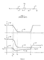
- FIG 1 shows the essential circuit elements for a BBD-type charge transfer.
- V x is an input voltage applied to the first terminal of capacitor 1.
- the second terminal of capacitor 1 and the source terminal of FET 2 are connected at node 4.
- the gate of FET 2 is connected to a voltage V G , presumed in this discussion to be held constant.
- the drain of FET 2 and first terminal of load capacitor 3 are connected at node 5.
- the other terminal of load capacitor 3 is connected to circuit common ('ground').
- FIG. 2 shows voltage waveforms associated with the circuit of Figure 1 .
- V x is at a high voltage 21; node 5 has been initialized to a relatively high voltage 23; and node 4 to a lower voltage 22.
- voltage 22 is more positive than V G - V T , where V T is the threshold of FET 2. Under these conditions FET 2 is biased below threshold, so no significant current flows through it.
- V 4 the voltage of node 4
- V 4 becomes equal to V G - V T , causing FET 2 to turn on.
- the resulting current flow through FET 2 limits further negative excursion of V 4 .
- V x reaches its lower value 24.
- Current continues to flow through FET 2 into capacitor 1, causing node 4 to charge in a positive direction.
- V 4 approaches V G -V T
- the current through FET 2 diminishes.
- V 4 settles towards V G - V T at a continuously-diminishing rate, reaching voltage 26 at time t 4 .
- V x is returned to its original voltage. This positive-going transition is coupled through capacitor 1 to node 4, causing FET 2 to turn off altogether and ending the charge transfer.
- Charge-transfer operation essentially similar to that described above is used in all conventional BBDs. Practical details, such as the means of establishing the described initial conditions, realistic clock waveforms, etc. are not pertinent to the present invention and will not be further described here.
- the same charge-transfer technique is also used to provide charge-packet input in many CCD signal-processing circuits. (Subsequent charge transfers in CCDs use a different principle, not described here.)
- Passive charge transfer The mode of charge-transfer described above will be termed "passive" charge transfer in the following discussion. This term refers to the fact that, during the charge-transfer process, the gate voltage V G applied to FET 2 is static, not actively controlled in response to the charge being transferred. (In practical BBDs, V G is typically clocked rather than static, but it is not responsive to the charge being transferred.) This passive charge transfer process is subject to two important error sources.
- the first error source derives from the nature of the settling of node 4 during the t 3 -to-t 4 interval in Figure 2 .
- node 4 is charging in a positive direction, reducing the gate-source voltage of FET 2.
- This decreasing gate-source voltage causes a decrease in current through the FET.
- This declining current in turn results in a declining rate of charging of node 4.
- This process is very non-linear in time, and also depends in a non-linear manner on the size of charge packet being transferred.
- the residual voltage 26 in Figure 2 (and Equation 6) depends non-linearly on Q T , resulting in an overall non-linear charge-transfer operation.
- the settling time of node 4 is unacceptably long for high-speed circuit operation. Passive charge-transfer is thus both slow and non-linear; in many applications these limitations degrade speed and accuracy unacceptably.
- the second error source arises due to the change ⁇ V 5 in FET drain voltage V 5 .
- this change is proportional to Q T .
- FETs exhibit a feedback effect, in which a variation in drain voltage causes, in effect, a variation in threshold voltage V T .
- the "final" voltage V G -V T towards which V 4 settles, is not in fact a constant (as in the idealized discussion above) but a function of the charge being transferred.
- This effect is equivalent to a dependency of voltage 26 on the size of Q T : larger
- This effect amounts to a charge-transfer gain of less than 100%. It typically includes a small non-linear component as well, exacerbating the non-linearity issue discussed above.
- Japanese Patent Publication No. 60149165 shows a circuit having an inversion amplifier introduced between a charge accumulation part and a transfer gate.
- the input is affected by both a pulse ⁇ D 1 coupled to a first terminal D 1 and a second pulse ⁇ C applied to a second terminal TC.
- the charge transfer channel carries an input charge Q s from a first stage, less an amount corresponding to V 1 , to a second stage.
- U.S. Patent 5,909,131 describes the use of resistive elements in an input holding device to reduce non-linear signal distortion during charge transfer.
- Embodiments of the present invention provide an apparatus for transferring charge according to independent claim 1 and a method for transferring charge according to independent claim 11 in which the effects of the two error sources described above are significantly reduced.
- the charge transfer method of the present invention is termed "boosted". The performance of a boosted charge-transfer circuit is sufficiently improved over that of the passive circuit that it makes high-speed, high-precision applications feasible.
- the present invention provides a charge-transfer circuit in which the effects of the two error sources described above are significantly reduced.
- the charge transfer method of the present invention is termed "boosted".
- the performance of a boosted charge-transfer circuit is sufficiently improved over that of the passive circuit that it makes high-speed, high-precision applications feasible.
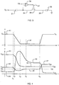
- This boosted charge-transfer technique can be understood with the aid of Figures 3 and 4 , which illustrate the basic features of its operation.
- Capacitor 31 in Figure 3 corresponds to capacitor 1 in Figure 1 , node 34 to node 4, etc.
- the added amplifier 36 is the unique feature of this invention; it has moderate voltage gain (typically 10-100) and very high speed.
- FIG. 4 The operating waveforms of this circuit are shown in Figure 4 , using the same naming conventions employed in Figure 2 (e.g., the voltage of node 34 is called V 34 , etc.).
- Initial conditions in Figure 4 are similar to those in Figure 2 .
- Input voltage V X starts at a high value, 41.
- Drain node 35 is initialized to a high voltage 43.
- Source node 34 is initialized to a lower voltage 42, which is more positive than V R .
- V 34 > V R amplifier 36 drives its output, node 37, to a low voltage 48.
- Node 37 is also connected to the gate of FET 32, so a low value of V 37 assures that FET 32 is initially turned off, and no current flows through it.
- V 34 follows V X in a negative direction.
- V 34 becomes more negative than V R , causing amplifier 36 to drive its output node 37 to a high voltage.
- This high voltage turns on FET 32; the resulting current through FET 32 limits the negative excursion of node 34.
- Amplifier 36 then operates, by feedback via FET 32, to maintain V 34 slightly below V R . This balance persists until time t 3 when V X reaches its lower value 44.
- the current flowing through FET 32 then charges node 34 positively until t 4 , when V 34 approaches V R .
- V 34 - V R As its input drive (V 34 - V R ) approaches zero, amplifier 36 drives its output voltage 37 towards a lower value 49, and the current through FET 32 declines rapidly. Finally, at time t 5 , V X is returned to its original value; this positive-going transition is coupled through capacitor 31 to node 34, causing amplifier 36 to again drive its output node 37 to a low voltage, turning FET 32 off and ending the charge transfer.
- V R the reference voltage for amplifier 36.
- V 34 the value of V 34 at the end of charge transfer (time t 5 ) is voltage 46.
- any difference between voltage 46 and V R represents an error in the transferred charge.
- the key difference between the boosted and passive charge transfer lies in the improved precision and speed with which V 34 approaches V R .
- Equation 12 Comparing Equation 12 to Equation 10 shows that the rate at which V GS settles is increased by the gain of amplifier 36 compared to the passive case. The time required after t 3 for settling to any given level of precision is similarly reduced. The non-linearity of the final voltage 46 is similarly reduced by approximately the same factor relative to final voltage 26 in Figure 2 .
- the gain of the amplifier in a boosted charge transfer circuit needs to be high enough to produce a significant improvement in linearity and speed.
- Voltage gain in the range of 10-100 produces substantial benefits.
- Significantly lower gain reduces the linearity improvement, and higher gain results in dynamic problems described in more detail below.
- Charge-transfer settling time is also related to the speed of the amplifier, as discussed below.
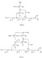
- Figure 5 shows a boosted charge-transfer circuit incorporating a basic CMOS amplifier which provides the needed performance.
- Elements V X , capacitors 51 and 53, and charge-transfer FET 52 are arranged just as in Figure 3 .
- the amplifier, 36 in Figure 3 is implemented in Figure 5 as common-source-connected NFET 56, and PFET 58 which is connected as a current source with positive supply V DD and bias voltage V B . Operation of this circuit is just as described in connection with Figures 3 and 4 .
- the equivalent in Figure 5 of amplifier reference voltage V R in Figure 3 is the voltage at node 54 at which the drain current of NFET 56 balances the drain current of PFET 58. This voltage is slightly above the threshold of NFET 56.
- This type of circuit can have voltage gain in the required range. Its speed can be chosen by scaling FETs 56 and 58 and their operating current: larger FETs and more current result in higher speed, with the limit being characteristic of the particular semiconductor fabrication process.
- the total capacitance contributing to noise generation includes three significant terms: the explicit value of capacitor 51; the gate-input capacitance of amplifier FET 56; and the capacitance from node 57 to node 54 multiplied by the gain of the amplifier.
- This latter capacitance term, which is multiplied by the amplifier gain, is sometimes referred to (for historical reasons) as "Miller" capacitance.
- it consists of the drain-to-gate capacitance of FET 56 plus the gate-to-source capacitance of FET 52. Even though the device parasitic capacitances of FETs 52 and 56 may be small compared with the value of capacitor 51, the fact that the Miller capacitance is multiplied by the amplifier gain can make it a significant noise issue in this circuit.
- Figure 6 shows a boosted charge-transfer circuit which improves upon the circuit of Figure 5 by reducing the Miller capacitance.
- the amplifier in the circuit of Figure 6 consists of the FETs 66 and 68, serving the same functions as FETs 56 and 58 in Figure 5 .
- a source-follower PFET 69 is added, supplied by a PFET current-source. Because it provides voltage buffering between node 64 and node 70, the contribution of the drain-to-gate capacitance of FET 66 to the Miller capacitance is largely eliminated.
- the gate-source capacitance of FET 62 contributes significantly to the Miller capacitance. The result is a corresponding reduction of kTC-noise generation relative to the circuit of Figure 5 .
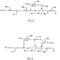
- FIG. 7 shows another boosted charge-transfer circuit with reduced Miller capacitance.
- This circuit is identical to that of Figure 5 , except that the NFET 79 is added between the drain of FET 76 and the amplifier output node 77.
- FET 79 acts as a common-gate amplifier, with its gate biased at a constant voltage V B2 .
- the common-source + common-gate composite of FETs 76 and 79 is the well-known "cascode" configuration. Its effect in this application is primarily to reduce the gain from gate to drain of FET 76 while maintaining or increasing gain from node 74 to node 77. While the drain-gate capacitance of FET 76 is not reduced, the gain which multiplies it is reduced, thus reducing its contribution to kTC-noise generation.
- the circuit does not have a DC "quiescent point" at which stable conditions can be established.
- the FET current drops to a sufficiently low level approaching t 5 , then current through the gate-source capacitance of FET 32 swamps the drain-source current, and the second pole is eliminated. Consequently the final settling of the circuit is unconditionally stable.
- the second-order response during the middle of the charge transfer can result in 'overshoot' at nodes 37 and 34, causing a non-linear disturbance of Q T .
- FIG 8 A solution to this problem is shown in Figure 8 .
- This circuit is identical to the basic boosted charge-transfer circuit of Figure 3 , with similarly-identified elements, except that the resistors 88 and 89 are added.
- the sum of these resistors adds a zero which partially cancels the second pole mentioned above, thus providing an adequately damped overall response. If the combined resistance is made larger than necessary, it reduces the speed of the charge-transfer operation, reducing the benefit of the boosted circuit. With practical circuit parameters, a significant range exists for an appropriate choice of resistor values. Either resistor 88 or 89 or a combination can be used to achieve the needed effect.
- FIG. 9 This circuit is identical to the basic circuit of Figure 3 , with similarly-identified elements, except for the addition of NFET 98 which is controlled by a logic voltage signal V OFF . When V OFF is high, FET 98 is turned on, and drives node 97 to near zero volts.
- node 94 can assume any initial voltage down to zero (or even slightly below zero) without causing FET 92 to turn on (because V GS of FET 92 is not significantly positive).
- V OFF is set low, then FET 98 is turned off.
- the circuit behaves just like that of Figure 3 : amplifier 96 can drive node 97 positive whenever the voltage of node 94 is less than V R , turning FET 92 on and allowing current flow. If V 94 ⁇ V R when V OFF goes low, then amplifier 96 will immediately begin driving node 97 high, initiating current flow. Similarly, setting V OFF high will terminate charge-transfer regardless of the state of V 94 . Applications of this capability will be discussed below.
- charge-transfer typically only happens during part of an overall operating cycle, often 50% or less.
- current flows only between t 1 and t 5 .
- the amplifier or a switch FET such as FET 98, just discussed holds the common-gate charge-transfer FET in an off state. In this state the amplifier is not required to respond to the input signal (at node 94, for example). Thus the current source or sources which are part of the amplifier can be disabled, eliminating power consumption. If current-flow control via a signal such as V OFF is used, the same signal can also be used to control power consumption.
- FIG. 10 An example of such a circuit is shown in Figure 10 .
- This circuit is similar to that of Figure 5 , with the addition of NFET 109 and PFET 110, both controlled by the logic voltage signal V OFF .
- V OFF When V OFF is high, FET 109 holds node 107 at a low voltage, disabling current flow though FET 102. At the same time, FET 110 is turned off, so no current flows through current-source FET 108; thus power consumption due to the amplifier is extinguished.
- V OFF is set low, then FET 110 turns on, enabling current flow through FET 108; and FET 109 turns off, allowing node 107 to rise and turn on FET 102, permitting signal charge to flow from node 104 to node 105.
- circuits of Figures 6 and 7 can be modified in ways similar to the modification just described, to disable charge transfer and eliminate power consumption by their amplifiers during the time when a control voltage V OFF is asserted.
- the input signal V X is represented as an abstract voltage source.
- the voltage at the charge-transfer FET's source, node 4 in Figure 1 for example is described as "initialized to voltage 22". Similar abstract initialization is assumed for the circuit of Figure 3 .
- this abstract representation sufficed.
- these abstractions must be replaced by realistic circuitry.
- An application example is shown in Figure 11 , in which the abstract voltage control is replaced by slightly less-abstract switches. In a fully-developed practical circuit, these switches would each be implemented as an NFET, a PFET, or an NFET-PFET combination known as a 'transmission gate'. The circuit details for controlling these switches are not considered in this discussion.
- Figure 11 shows a boosted charge-transfer circuit similar to that of Figure 3 , with three additional elements: switches 119, 120, and 121.
- the node driven by V X in Figure 3 is here labeled node 118.
- This circuit provides a voltage-to-charge sample-and-hold function, in which an output charge packet Q T delivered to capacitor 113 is a linear function of the three input voltages V 1 , V 2 , and V 3 .
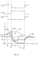
- One mode of operation of this circuit is described with the aid of Figure 12 . This operation is very similar to that of the circuit of Figure 3 , whose waveforms are shown in Figure 4 .
- FIG 12 three switch states and two voltages are plotted against time.
- the switch states S 119 , S 120 and S 121 respectively represent the states of switches 119, 120, and 121 in Figure 11 .
- a high value for a switch state indicates that the switch is on, and a low value indicates off.
- the voltages of nodes 118 and 114 are plotted below the switch states.
- Six times to - t 5 are identified. Times t 1 - t 5 correspond to the five times identified in Figure 4 , emphasizing the similarity of operation of the circuits of Figure 3 and Figure 11 . Initially, switches 119 and 121 are on; switch 120 is off.
- node 118 is connected to V 2 , whose value is identified as 123 in Figure 12 ; and node 114 is connected to V 3 , whose value is identified as 122 in Figure 12 .
- voltages 123 and 122 correspond to initial voltages 41 and 42 in Figure 4 .
- switch 121 turns off, leaving node 114 at voltage 122 (since no current is yet flowing through FET 112).
- switch 119 turns off and switch 120 turns on, connecting node 118 to V 1 .
- Node 118 charges towards V 1 with a time constant governed by the on-resistance of switch 120, eventually reaching a settled voltage 124 equal to V 1 .
- V 118 's waveform is similar to that of V X in Figure 4 .
- V 114 initially follows V 118 , then stops when current flows through FET 112, and eventually settles to a voltage 126 which is very close to V R .
- all three switches return to their original states, re-connecting node 118 to V 2 and node 114 to V 3 , and ending the charge transfer process.
- switches 119 and 121 are turned on.
- Switch 121 holds node 114 at voltage 132 (equal to the value of V 3 ) as in the foregoing discussion.
- Switch 119 connects node 118 to the time-varying voltage source V 2 , so that the voltage of node 118 tracks V 2 .
- the time constant of switch 119 and capacitor 111 is assumed short enough to be neglected compared to the rate of change of V 2 .
- At to switch 121 turns off. Since node 114 is no longer connected to V 3 , it follows node 118 due to coupling through capacitor 111 (note that in Figure 12 node 118 was static, so V 114 did not change at this point).
- Equation 18 the amount of charge delivered by capacitor 111 during charge-transfer is simply the change in its voltage multiplied by its capacitance.
- the initial voltage (before charge transfer) is given by Equation 18, and the final voltage by Equation 19.
- Equation 20 has exactly the same form as Equation 17, with the static value of V 2 in Equation 17 replaced by the sampled value at to in Equation 20. This is the desired sample-and-hold property.
- V 2 is static, this circuit can be used to generate a sequence of charge packets of uniform size controlled by V 2 's value (together with the values of V 1 , V 3 and V R ). If V 2 is time-varying, then the result is sampling of V 2 under control of a (clock) signal S 121 . As Equation 21 shows, the resulting charge packets contain the sampled charge plus a constant term. This constant term is adjustable by varying the values of V 1 , V 3 , and/or V R .
- the transferred charge Q T is collected by an output capacitor, for example C33 in Figure 3 .
- the transferred charge can instead be collected in a storage well of a charge-coupled device (CCD).
- CCD charge-coupled device
- Figure 14A shows a boosted charge-transfer circuit similar to that of Figure 3 , in which the charge-transfer FET and the output capacitor are replaced with CCD elements.
- V X , capacitor 141, node 144, reference voltage V R , amplifier 146 and amplifier-output node 147 are all precisely analogous to their equivalents in Figure 3 .
- the new feature in Figure 14A is CCD 148, consisting of an input terminal connected to node 144 and three gates 142, 143 and 145. (In a practical implementation, the CCD would typically have additional gates beyond gate 145. Three gates suffice to describe the function of this circuit.)
- FIG. 14B A cross-section representation of the device structure of CCD 148 is shown in Figure 14B .
- the input terminal consists of diffusion 149 which has opposite conductivity type to the semiconductor substrate 150.
- the three gates 142, 143 and 145 are adjacent electrodes, separated from the substrate by a gate dielectric layer, and from each other by dielectric-filled gaps.
- the CCD schematic symbol used in Figure 14A corresponds feature-for-feature with the structure shown in Figure 14B .
- the structure shown is typical of single-poly CCDs; double-poly and other CCD structures are well-known, and could be used as well in the circuit of Figure 14A .
- node 144 is connected to the input terminal 149 of CCD 148.
- This terminal functions like the source of FET 32 in Figure 3 .
- the first gate, 142, of CCD 148 is connected to amplifier-output node 147.
- This gate functions like the gate of FET 32 in Figure 3 , by controlling the flow of current from node 144 into the CCD.
- Clock voltage ⁇ 1 when driven to a high voltage, creates a potential well under gate 143.
- This well is analogous to the drain of FET 32 together with capacitor 33 in Figure 3 : current flowing under gate 142 collects as charge in the well under gate 143, just as current flowing through FET 32 in Figure 3 collects as charge on capacitor 33.
- clock voltage ⁇ 2 biases gate 145 off, preventing current from flowing further along the CCD; thus all current flowing under gate 142 is collected in the potential well under gate 143.
- the initial condition for the potential well under gate 143 is zero charge.
- the operation and timing of the circuit of Figure 14A are identical to those of Figure 4 , except for the aforementioned difference in the means of collection of transferred charge.
- the transferred charge Q T has is accumulated under gate 143, and gate 142 is driven off by amplifier 146.
- Q T can be transferred along CCD 148 by appropriate clocking of ⁇ 1 and ⁇ 2 using well-known CCD methods which are not part of this invention.
- All circuits discussed above are shown in single-ended configurations; that is, all voltages are referred to a common reference ('ground'), and all charge packets can have only one sign. (In the case of electrons as charge carriers, the charge packets are always negative; the maximum packet, in algebraic terms, is zero.) It is common to employ differential circuits in practical circuit applications, to provide symmetrical means of representing variables with either sign, for suppression of second-harmonic distortion, and for other reasons.
- the charge-transfer circuits discussed above can all be used in so-called 'quasi-differential' configurations using a pair of charge packets.
- the signal is represented as the difference between the two members of the charge-packet pair; each member of the pair also has a bias- or common-mode charge in addition to the signal component.
- Such circuit configurations are implemented using pairs of the charge-transfer circuits shown, one such circuit to handle each of the members of the charge-packet pair.
Description
- This application claims the benefit of
U.S. Provisional Application No. 60/809,485, filed on May 31, 2006 - In charge-domain signal-processing circuits, signals are represented as charge packets. These charge packets are stored, transferred from one storage location to another, and otherwise processed to carry out specific signal-processing functions. Charge packets are capable of representing analog quantities, with the charge-packet size in coulombs being proportional to the signal represented. Charge-domain operations such as charge-transfer are driven by 'clock' voltages, providing discrete-time processing. Thus, charge-domain circuits provide analog, discrete-time signal-processing capability.
- Charge-domain circuits are implemented as charge-coupled devices (CCDs), as Metal Oxide Semiconductor (MOS) bucket-brigade devices (BBDs), and as bipolar BBDs. The present invention pertains primarily to MOS BBDs; it also has application to CCDs, in the area of charge-packet creation. Note that all circuits discussed below assume electrons as the signal-charge carriers, and use N-Channel Field Effect Transistors (NFETs) or N-channel CCDs for signal-charge processing. The identical circuits can be applied equally well using holes as charge carriers, by employing PFETs or P-channel CCDs and with reversed signal and control voltage polarities.
- In MOS BBDs the charge packets are stored on capacitors. Charge transfer from one storage capacitor to the next occurs via a FET connected in common-gate configuration. The process of charge transfer in a BBD is explained with the aid of
Figure 1 and Figure 2 . These figures omit many practical details, but they suffice to show the essential features of charge transfer in conventional BBDs. -
Figure 1 shows the essential circuit elements for a BBD-type charge transfer. InFigure 1 Vx is an input voltage applied to the first terminal ofcapacitor 1. The second terminal ofcapacitor 1 and the source terminal of FET 2 are connected atnode 4. The gate ofFET 2 is connected to a voltage VG, presumed in this discussion to be held constant. The drain ofFET 2 and first terminal of load capacitor 3 are connected atnode 5. The other terminal of load capacitor 3 is connected to circuit common ('ground'). -
Figure 2 shows voltage waveforms associated with the circuit ofFigure 1 . At the beginning of a charge-transfer cycle Vx is at ahigh voltage 21;node 5 has been initialized to a relativelyhigh voltage 23; andnode 4 to alower voltage 22. For this basic explanation, it is assumed thatvoltage 22 is more positive than VG - VT, where VT is the threshold ofFET 2. Under theseconditions FET 2 is biased below threshold, so no significant current flows through it. - The charge transfer is initiated at time t1 by lowering Vx towards a more negative voltage. Initially, V4, the voltage of
node 4, follows Vx in a negative direction. At time t2, V4 becomes equal to VG - VT, causingFET 2 to turn on. The resulting current flow through FET 2 limits further negative excursion of V4. At time t3 Vx reaches itslower value 24. Current continues to flow throughFET 2 intocapacitor 1, causingnode 4 to charge in a positive direction. As V4 approaches VG-VT, the current throughFET 2 diminishes. V4 settles towards VG - VT at a continuously-diminishing rate, reachingvoltage 26 at time t4 . At t4 Vx is returned to its original voltage. This positive-going transition is coupled throughcapacitor 1 tonode 4, causingFET 2 to turn off altogether and ending the charge transfer. - During the events described, current flows from capacitor 3 through
FET 2 intocapacitor 1. The integral of this current flow constitutes the transferred charge, QT. QT can be expressed in terms of the voltage changes and respective capacitances at Vx,node 4, andnode 5. Neglecting the device capacitances ofFET 2, the charge delivered to capacitor 3 can be expressed in terms of the voltage change across it, using the well-known expression Q = CV. Identifying the capacitance of capacitor 3 as C3 and the voltage change atnode 5 as ΔV5, we have:
- QT can also be expressed in terms of the voltage change across
capacitor 1. Using similar notation, we have:
Figure 2 ,

- For the conditions described,
voltage 22 is a constant (it is an initial condition). Ifnode 4 were to settle perfectly to its nominal asymptote VG - VT, which is also a constant, then ΔV4 would be a constant. In that case,Equation 2 could be re-written as:
node 4 is imperfect,Equation 2 can be re-formulated as:
voltage 26, the voltage ofnode 4 at the end of charge-transfer. - Charge-transfer operation essentially similar to that described above is used in all conventional BBDs. Practical details, such as the means of establishing the described initial conditions, realistic clock waveforms, etc. are not pertinent to the present invention and will not be further described here. The same charge-transfer technique is also used to provide charge-packet input in many CCD signal-processing circuits. (Subsequent charge transfers in CCDs use a different principle, not described here.)
- The mode of charge-transfer described above will be termed "passive" charge transfer in the following discussion. This term refers to the fact that, during the charge-transfer process, the gate voltage VG applied to
FET 2 is static, not actively controlled in response to the charge being transferred. (In practical BBDs, VG is typically clocked rather than static, but it is not responsive to the charge being transferred.) This passive charge transfer process is subject to two important error sources. - The first error source derives from the nature of the settling of
node 4 during the t3-to-t4 interval inFigure 2 . During this time, as described above,node 4 is charging in a positive direction, reducing the gate-source voltage ofFET 2. This decreasing gate-source voltage causes a decrease in current through the FET. This declining current in turn results in a declining rate of charging ofnode 4. This process is very non-linear in time, and also depends in a non-linear manner on the size of charge packet being transferred. As a result, theresidual voltage 26 inFigure 2 (and Equation 6) depends non-linearly on QT, resulting in an overall non-linear charge-transfer operation. Moreover, with practical circuit values, the settling time ofnode 4 is unacceptably long for high-speed circuit operation. Passive charge-transfer is thus both slow and non-linear; in many applications these limitations degrade speed and accuracy unacceptably. - The second error source arises due to the change ΔV5 in FET drain voltage V5. As shown above (Equation 1) this change is proportional to QT. FETs exhibit a feedback effect, in which a variation in drain voltage causes, in effect, a variation in threshold voltage VT. Thus the "final" voltage VG-VT, towards which V4 settles, is not in fact a constant (as in the idealized discussion above) but a function of the charge being transferred. This effect is equivalent to a dependency of
voltage 26 on the size of QT: larger |QT| results in a more-negative value ofvoltage 26. This effect amounts to a charge-transfer gain of less than 100%. It typically includes a small non-linear component as well, exacerbating the non-linearity issue discussed above. - Japanese Patent Publication No.
60149165 -
U.S. Patent 5,909,131 describes the use of resistive elements in an input holding device to reduce non-linear signal distortion during charge transfer. - Embodiments of the present invention provide an apparatus for transferring charge according to
independent claim 1 and a method for transferring charge according toindependent claim 11 in which the effects of the two error sources described above are significantly reduced. In contrast to the passive charge transfer used in conventional BBDs, the charge transfer method of the present invention is termed "boosted". The performance of a boosted charge-transfer circuit is sufficiently improved over that of the passive circuit that it makes high-speed, high-precision applications feasible. - The foregoing will be apparent from the following more particular description of example embodiments of the invention, as illustrated in the accompanying drawings in which like reference characters refer to the same parts throughout the different views. The drawings are not necessarily to scale, emphasis instead being placed upon illustrating embodiments of the present invention.
-
Figure 1 is a simplified diagram of a charge transfer circuit. -
Figure 2 illustrates voltage waveforms associated withFigure 1 . -
Figure 3 is a boosted charge transfer circuit according to aspects of the invention. -
Figure 4 illustrates voltage waveforms for the circuit ofFigure 3 . -
Figure 5 is a boosted charge transfer circuit incorporating a CMOS amplifier. -
Figure 6 is another boosted charge transfer circuit using an amplifier that reduces Miller capacitance. -
Figure 7 is a boosted charge transfer circuit that uses an NFET as a common gate amplifier. -
Figure 8 is a boosted charge transfer circuit that uses resistor elements to dampen the circuit response. -
Figure 9 is a boosted charge transfer circuit that provides greater control over start and end of current flow. -
Figure 10 is a boosted charge transfer circuit using an FET that controls power consumption. -
Figure 11 is a boosted charge transfer circuit that provides a voltage-to-charge sample-and-hold function. -
Figure 12 illustrates voltage waveforms associated with the circuit ofFigure 11 in the case of static input voltage.. -
Figure 13 illustrates voltage waveforms associated with the circuit ofFigure 12 in the case of time-varying input voltage. -
Figure 14A and 14B are a circuit diagram and cross-sectional device structure diagram of a boosted charge transfer circuit which provides input charge to a CCD. - A description of preferred embodiments of the invention follows.
- The present invention provides a charge-transfer circuit in which the effects of the two error sources described above are significantly reduced. In contrast to the passive charge transfer used in conventional BBDs, the charge transfer method of the present invention is termed "boosted". The performance of a boosted charge-transfer circuit is sufficiently improved over that of the passive circuit that it makes high-speed, high-precision applications feasible. This boosted charge-transfer technique can be understood with the aid of
Figures 3 and 4 , which illustrate the basic features of its operation. - The elements of
Figure 3 are the same as similarly-identified elements ofFigure 1 , except for the addition ofamplifier 36 and its reference voltage VR, and the omission of voltage VG. Capacitor 31 inFigure 3 corresponds tocapacitor 1 inFigure 1 ,node 34 tonode 4, etc. The addedamplifier 36 is the unique feature of this invention; it has moderate voltage gain (typically 10-100) and very high speed. - The operating waveforms of this circuit are shown in
Figure 4 , using the same naming conventions employed inFigure 2 (e.g., the voltage ofnode 34 is called V34, etc.). Initial conditions inFigure 4 are similar to those inFigure 2 . Input voltage VX starts at a high value, 41.Drain node 35 is initialized to ahigh voltage 43.Source node 34 is initialized to alower voltage 42, which is more positive than VR. Because V34 > VR,amplifier 36 drives its output,node 37, to alow voltage 48.Node 37 is also connected to the gate ofFET 32, so a low value of V37 assures thatFET 32 is initially turned off, and no current flows through it. - The charge transfer is initiated at time t1 by lowering VX towards a more negative voltage. Initially, V34 follows VX in a negative direction. At time t2, V34 becomes more negative than VR, causing
amplifier 36 to drive itsoutput node 37 to a high voltage. This high voltage turns onFET 32; the resulting current throughFET 32 limits the negative excursion ofnode 34.Amplifier 36 then operates, by feedback viaFET 32, to maintain V34 slightly below VR. This balance persists until time t3 when VX reaches itslower value 44. The current flowing throughFET 32 then chargesnode 34 positively until t4, when V34 approaches VR. As its input drive (V34 - VR) approaches zero,amplifier 36 drives itsoutput voltage 37 towards alower value 49, and the current throughFET 32 declines rapidly. Finally, at time t5, VX is returned to its original value; this positive-going transition is coupled throughcapacitor 31 tonode 34, causingamplifier 36 to again drive itsoutput node 37 to a low voltage, turningFET 32 off and ending the charge transfer. - As with the passive charge transfer previously described, the current flowing through
FET 32 is integrated bycapacitor 33, resulting in the voltage waveform V35 atnode 35. This integrated current constitutes the transferred charge, QT. The charge and voltage oncapacitor 33 are related just as in Equation 1:
- Where ΔV35 = (voltage 45 - voltage 43).
- Similarly,

- And by analogy with Equation 6,

- The asymptote towards which V34 settles is VR, the reference voltage for
amplifier 36. InFigure 4 the value of V34 at the end of charge transfer (time t5) isvoltage 46. As with the passive charge transfer, any difference betweenvoltage 46 and VR represents an error in the transferred charge. The key difference between the boosted and passive charge transfer lies in the improved precision and speed with which V34 approaches VR. - In both passive and boosted charge-transfer circuits, the source voltage of the FET (
nodes Figures 1 and3 respectively) is charged positively by the FET current after t3. This charging results in decreasing gate-source voltage VGS and FET current ID, as described above. In the passive circuit ofFigure 1 , the gate voltage VG is fixed, so the rate of change of VGS is simply the negative of that of V4:
Figure 3 , the same equation applies (to V34 and C31 respectively). However, the gate ofFET 32 is not held at a constant voltage, but driven by the output ofamplifier 36, which responds to the voltage atnode 34 with gain A (typically 10-100 as mentioned above). Thus the gate-source voltage ofFET 32 is:
- Since VR is constant, the rate of change of VGS for the boosted charge transfer circuit of
Figure 3 is thus:
- Comparing Equation 12 to Equation 10 shows that the rate at which VGS settles is increased by the gain of
amplifier 36 compared to the passive case. The time required after t3 for settling to any given level of precision is similarly reduced. The non-linearity of thefinal voltage 46 is similarly reduced by approximately the same factor relative tofinal voltage 26 inFigure 2 . - In the preceding material, a number of important circuit details were omitted for the sake of clarity in the basic explanation. These details are described in the following paragraphs.
- As stated above, the gain of the amplifier in a boosted charge transfer circuit, such as
amplifier 36 inFigure 3 , needs to be high enough to produce a significant improvement in linearity and speed. Voltage gain in the range of 10-100 produces substantial benefits. Significantly lower gain reduces the linearity improvement, and higher gain results in dynamic problems described in more detail below. Charge-transfer settling time is also related to the speed of the amplifier, as discussed below. Thus design of the amplifier is constrained by the dual requirements of medium gain and very high speed. Several practical circuits which satisfy these constraints are described below. -
Figure 5 shows a boosted charge-transfer circuit incorporating a basic CMOS amplifier which provides the needed performance. Elements VX,capacitors transfer FET 52 are arranged just as inFigure 3 . The amplifier, 36 inFigure 3 , is implemented inFigure 5 as common-source-connectedNFET 56, andPFET 58 which is connected as a current source with positive supply VDD and bias voltage VB. Operation of this circuit is just as described in connection withFigures 3 and 4 . The equivalent inFigure 5 of amplifier reference voltage VR inFigure 3 is the voltage atnode 54 at which the drain current of NFET 56 balances the drain current ofPFET 58. This voltage is slightly above the threshold ofNFET 56. This type of circuit can have voltage gain in the required range. Its speed can be chosen by scalingFETs - While suitable for some applications, the circuit of
Figure 5 has a significant performance limitation. All charge-transfer circuits add thermal noise to the transferred charge packet. This added noise is often referred to as "kTC" noise, because in simple cases it obeys the law:
Equation 13 applies, for example, to the passive charge-transfer circuit ofFigure 1 , where the pertinent C is that ofcapacitor 1, plus the previously-neglected parasitic capacitances atnode 4. (In some cases the noise added by the circuit ofFigure 1 may be slightly less than the amount indicated byEquation 13.) - In the circuit of
Figure 5 , the total capacitance contributing to noise generation includes three significant terms: the explicit value ofcapacitor 51; the gate-input capacitance ofamplifier FET 56; and the capacitance fromnode 57 tonode 54 multiplied by the gain of the amplifier. This latter capacitance term, which is multiplied by the amplifier gain, is sometimes referred to (for historical reasons) as "Miller" capacitance. InFigure 5 it consists of the drain-to-gate capacitance ofFET 56 plus the gate-to-source capacitance ofFET 52. Even though the device parasitic capacitances ofFETs capacitor 51, the fact that the Miller capacitance is multiplied by the amplifier gain can make it a significant noise issue in this circuit. -
Figure 6 shows a boosted charge-transfer circuit which improves upon the circuit ofFigure 5 by reducing the Miller capacitance. The amplifier in the circuit ofFigure 6 consists of theFETs FETs Figure 5 . InFigure 6 a source-follower PFET 69 is added, supplied by a PFET current-source. Because it provides voltage buffering betweennode 64 andnode 70, the contribution of the drain-to-gate capacitance ofFET 66 to the Miller capacitance is largely eliminated. Thus inFigure 6 only the gate-source capacitance ofFET 62 contributes significantly to the Miller capacitance. The result is a corresponding reduction of kTC-noise generation relative to the circuit ofFigure 5 . -
Figure 7 shows another boosted charge-transfer circuit with reduced Miller capacitance. This circuit is identical to that ofFigure 5 , except that theNFET 79 is added between the drain ofFET 76 and theamplifier output node 77.FET 79 acts as a common-gate amplifier, with its gate biased at a constant voltage VB2. The common-source + common-gate composite ofFETs FET 76 while maintaining or increasing gain fromnode 74 tonode 77. While the drain-gate capacitance ofFET 76 is not reduced, the gain which multiplies it is reduced, thus reducing its contribution to kTC-noise generation. - One significant problem with the boosted charge-transfer circuit was alluded to above but not detailed there: the dynamic behavior of the circuits so far discussed may exhibit a type of instability which can disrupt the desired linear charge-transfer. This problem arises especially in the case of relatively high amplifier gain, which is otherwise desirable in order to reduce nonlinearity.
- This dynamic problem arises during the early part of the charge transfer, between t2 and t4 in
Figure 4 . In this region, the closed loop seen inFigure 3 fromnode 34, throughamplifier 36 tonode 37, throughFET 32 back tonode 34, exhibits a 2-pole (second-order) gain characteristic. One pole is due to the gm of the amplifier and the capacitance atnode 37; the other is due to the gm ofFET 32 andcapacitor 1. It is apparent that second-order loop gain is intrinsic to this basic circuit topology. Because the current throughFET 32 starts at zero before t2, rises to a peak, and then decays during the t3-t5 interval to a very small value, the circuit does not have a DC "quiescent point" at which stable conditions can be established. When the FET current drops to a sufficiently low level approaching t5, then current through the gate-source capacitance ofFET 32 swamps the drain-source current, and the second pole is eliminated. Consequently the final settling of the circuit is unconditionally stable. The second-order response during the middle of the charge transfer can result in 'overshoot' atnodes - A solution to this problem is shown in
Figure 8 . This circuit is identical to the basic boosted charge-transfer circuit ofFigure 3 , with similarly-identified elements, except that theresistors resistor - In the discussion of
Figures 3-4 the initial voltage atnode 34 was chosen to assure thatFET 32 was turned off. Thus no current flowed through the FET until after t1 when VX began changing. Likewise, current flow ended when VX returned to its initial value. In some applications of boosted charge transfer it is desirable to control the start and end of current flow by other means. One such means is shown inFigure 9 . This circuit is identical to the basic circuit ofFigure 3 , with similarly-identified elements, except for the addition of NFET 98 which is controlled by a logic voltage signal VOFF. When VOFF is high,FET 98 is turned on, and drivesnode 97 to near zero volts. Thusnode 94 can assume any initial voltage down to zero (or even slightly below zero) without causingFET 92 to turn on (because VGS ofFET 92 is not significantly positive). When VOFF is set low, thenFET 98 is turned off. In this condition the circuit behaves just like that ofFigure 3 :amplifier 96 can drivenode 97 positive whenever the voltage ofnode 94 is less than VR, turningFET 92 on and allowing current flow. If V94<VR when VOFF goes low, then amplifier 96 will immediately begin drivingnode 97 high, initiating current flow. Similarly, setting VOFF high will terminate charge-transfer regardless of the state of V94. Applications of this capability will be discussed below. - Consideration of the detailed amplifier circuits in
Figures 5, 6 , and7 shows that a FET connected as shown inFigure 9 can also be used in each specific case to achieve the results described for the more abstract circuit ofFigure 9 . - In many applications it is desirable to minimize overall circuit power consumption. In a boosted charge-transfer circuit, charge-transfer typically only happens during part of an overall operating cycle, often 50% or less. In
Figure 4 , for example, current flows only between t1 and t5. During the remainder of the operating cycle, the amplifier (or a switch FET such asFET 98, just discussed) holds the common-gate charge-transfer FET in an off state. In this state the amplifier is not required to respond to the input signal (atnode 94, for example). Thus the current source or sources which are part of the amplifier can be disabled, eliminating power consumption. If current-flow control via a signal such as VOFF is used, the same signal can also be used to control power consumption. - An example of such a circuit is shown in
Figure 10 . This circuit is similar to that ofFigure 5 , with the addition ofNFET 109 andPFET 110, both controlled by the logic voltage signal VOFF. When VOFF is high,FET 109 holdsnode 107 at a low voltage, disabling current flow thoughFET 102. At the same time,FET 110 is turned off, so no current flows through current-source FET 108; thus power consumption due to the amplifier is extinguished. When VOFF is set low, thenFET 110 turns on, enabling current flow throughFET 108; andFET 109 turns off, allowingnode 107 to rise and turn onFET 102, permitting signal charge to flow fromnode 104 tonode 105. - The circuits of
Figures 6 and7 can be modified in ways similar to the modification just described, to disable charge transfer and eliminate power consumption by their amplifiers during the time when a control voltage VOFF is asserted. - In all the charge-transfer circuits described above, the input signal VX is represented as an abstract voltage source. Also, the voltage at the charge-transfer FET's source,
node 4 inFigure 1 for example, is described as "initialized tovoltage 22". Similar abstract initialization is assumed for the circuit ofFigure 3 . For purposes of understanding the charge-transfer circuit principles discussed so far, this abstract representation sufficed. In actual applications of boosted charge-transfer circuits, however, these abstractions must be replaced by realistic circuitry. An application example is shown inFigure 11 , in which the abstract voltage control is replaced by slightly less-abstract switches. In a fully-developed practical circuit, these switches would each be implemented as an NFET, a PFET, or an NFET-PFET combination known as a 'transmission gate'. The circuit details for controlling these switches are not considered in this discussion. -
Figure 11 shows a boosted charge-transfer circuit similar to that ofFigure 3 , with three additional elements:switches Figure 3 is here labelednode 118. This circuit provides a voltage-to-charge sample-and-hold function, in which an output charge packet QT delivered tocapacitor 113 is a linear function of the three input voltages V1, V2, and V3. One mode of operation of this circuit is described with the aid ofFigure 12 . This operation is very similar to that of the circuit ofFigure 3 , whose waveforms are shown inFigure 4 . - In
Figure 12 , three switch states and two voltages are plotted against time. The switch states S119, S120 and S121 respectively represent the states ofswitches Figure 11 . A high value for a switch state indicates that the switch is on, and a low value indicates off. The voltages ofnodes Figure 4 , emphasizing the similarity of operation of the circuits ofFigure 3 andFigure 11 . Initially, switches 119 and 121 are on;switch 120 is off. Consequentlynode 118 is connected to V2, whose value is identified as 123 inFigure 12 ; andnode 114 is connected to V3, whose value is identified as 122 inFigure 12 . Thus voltages 123 and 122 correspond toinitial voltages Figure 4 . - At to switch 121 turns off, leaving
node 114 at voltage 122 (since no current is yet flowing through FET 112). At t1 switch 119 turns off and switch 120 turns on, connectingnode 118 to V1. Node 118 charges towards V1 with a time constant governed by the on-resistance ofswitch 120, eventually reaching a settledvoltage 124 equal to V1. V118's waveform is similar to that of VX inFigure 4 . Similarly, as with V34 inFigure 4 , V114 initially follows V118, then stops when current flows throughFET 112, and eventually settles to avoltage 126 which is very close to VR. At t5, all three switches return to their original states, re-connectingnode 118 to V2 andnode 114 to V3, and ending the charge transfer process. - Following the analysis applied to
Figures 3 and 4 , we can write an expression for the resulting output charge QT which is collected bycapacitor 113. By analogy with Equation 8:
Figure 12 :

voltage 126 and VR. - Combining these equations, we have:

- This expression shows that QT depends linearly on the four voltages V1, V2, V3 and VR, within the approximation in equation 16. The parasitic capacitance and charge transfer associated with
switch 121, and other parasitic capacitances atnode 114, have been neglected in this analysis. Their effect is to add offsets to the expression for QT, but the result remains linear in the four voltages. - The waveforms in
Figure 12 are implicitly based on the assumption that all four voltages in Equation 17 were static during the time shown.Figure 13 shows what happens if V2 is time-varying while V1, V3 and VR remain fixed. In this situation, it will be seen that the circuit ofFigure 11 generates an output charge QT which depends on the value of V2 at the moment when S121 turns off. Thus this circuit provides a voltage-to-charge sample-and-hold function. - For t < t0 in
Figure 13 ,switches Switch 121 holdsnode 114 at voltage 132 (equal to the value of V3) as in the foregoing discussion.Switch 119 connectsnode 118 to the time-varying voltage source V2, so that the voltage ofnode 118 tracks V2. (The time constant ofswitch 119 andcapacitor 111 is assumed short enough to be neglected compared to the rate of change of V2.) At to switch 121 turns off. Sincenode 114 is no longer connected to V3, it followsnode 118 due to coupling through capacitor 111 (note that inFigure 12 node 118 was static, so V114 did not change at this point). Neglecting parasitic capacitances, the voltage acrosscapacitor 111 remains constant and equal to its value at to. Specifically, takingnode 118 as the positive terminal of capacitor 111:
switch 119 turns off and switch 120 turns on.Node 118 is then driven towards voltage V1 (voltage 134) as inFigure 12 . As inFigure 12 ,node 114 initially followsnode 118, then stops when current flows throughFET 112, and eventually settles to avoltage 136 which is very close to VR. As above, charge transfer stops at t5 when the switches return to their initial state.Node 114 is re-connected to V3 and returns to itsinitial value 132.Node 118 is re-connected to V2, and settles to V2's then-current value 139. - The voltage across
capacitor 111 at the end of charge transfer (t5) is:
- As with the discussion of
Equation 1, we note that the amount of charge delivered bycapacitor 111 during charge-transfer is simply the change in its voltage multiplied by its capacitance. The initial voltage (before charge transfer) is given by Equation 18, and the final voltage by Equation 19. Thus:
- Equation 20 has exactly the same form as Equation 17, with the static value of V2 in Equation 17 replaced by the sampled value at to in Equation 20. This is the desired sample-and-hold property.
- Note that, if V1, V3, and VR are constant as assumed above, then the voltage-to-charge transfer function of Equation 20 can be written:

- If V2 is static, this circuit can be used to generate a sequence of charge packets of uniform size controlled by V2's value (together with the values of V1, V3 and VR). If V2 is time-varying, then the result is sampling of V2 under control of a (clock) signal S121. As
Equation 21 shows, the resulting charge packets contain the sampled charge plus a constant term. This constant term is adjustable by varying the values of V1, V3, and/or VR. - In all of the circuits discussed above, the transferred charge QT is collected by an output capacitor, for example C33 in
Figure 3 . In another application of the boosted charge-transfer circuit, the transferred charge can instead be collected in a storage well of a charge-coupled device (CCD). As just discussed, this capability can be used either for creating a series of constant (adjustable) charge packets, or for producing a series of charge packets which are proportional to samples of a time-varying voltage signal. -
Figure 14A shows a boosted charge-transfer circuit similar to that ofFigure 3 , in which the charge-transfer FET and the output capacitor are replaced with CCD elements. VX,capacitor 141,node 144, reference voltage VR,amplifier 146 and amplifier-output node 147 are all precisely analogous to their equivalents inFigure 3 . The new feature inFigure 14A isCCD 148, consisting of an input terminal connected tonode 144 and threegates gate 145. Three gates suffice to describe the function of this circuit.) - A cross-section representation of the device structure of
CCD 148 is shown inFigure 14B . The input terminal consists ofdiffusion 149 which has opposite conductivity type to the semiconductor substrate 150. The threegates Figure 14A corresponds feature-for-feature with the structure shown inFigure 14B . The structure shown is typical of single-poly CCDs; double-poly and other CCD structures are well-known, and could be used as well in the circuit ofFigure 14A . - In
Figure 14A node 144 is connected to theinput terminal 149 ofCCD 148. This terminal functions like the source ofFET 32 inFigure 3 . The first gate, 142, ofCCD 148 is connected to amplifier-output node 147. This gate functions like the gate ofFET 32 inFigure 3 , by controlling the flow of current fromnode 144 into the CCD. Clock voltage Φ1, when driven to a high voltage, creates a potential well undergate 143. This well is analogous to the drain ofFET 32 together withcapacitor 33 inFigure 3 : current flowing undergate 142 collects as charge in the well undergate 143, just as current flowing throughFET 32 inFigure 3 collects as charge oncapacitor 33. During charge-transfer, clock voltage Φ2 biases gate 145 off, preventing current from flowing further along the CCD; thus all current flowing undergate 142 is collected in the potential well undergate 143. - The initial condition for the potential well under
gate 143 is zero charge. The operation and timing of the circuit ofFigure 14A are identical to those ofFigure 4 , except for the aforementioned difference in the means of collection of transferred charge. At the end of the charge-transfer operation (t5 inFigure 4 ) the transferred charge QT has is accumulated undergate 143, andgate 142 is driven off byamplifier 146. Subsequently QT can be transferred alongCCD 148 by appropriate clocking of Φ1 and Φ2 using well-known CCD methods which are not part of this invention. - All circuits discussed above are shown in single-ended configurations; that is, all voltages are referred to a common reference ('ground'), and all charge packets can have only one sign. (In the case of electrons as charge carriers, the charge packets are always negative; the maximum packet, in algebraic terms, is zero.) It is common to employ differential circuits in practical circuit applications, to provide symmetrical means of representing variables with either sign, for suppression of second-harmonic distortion, and for other reasons. The charge-transfer circuits discussed above can all be used in so-called 'quasi-differential' configurations using a pair of charge packets. In such configurations, the signal is represented as the difference between the two members of the charge-packet pair; each member of the pair also has a bias- or common-mode charge in addition to the signal component. Such circuit configurations are implemented using pairs of the charge-transfer circuits shown, one such circuit to handle each of the members of the charge-packet pair.
- While this invention has been particularly shown and described with references to preferred embodiments thereof, it will be understood by those skilled in the art that various changes in form and details may be made therein without departing from the scope of the invention as defined by the appended claims.
Claims (15)
- An apparatus for transferring charge, comprising:an input charge holding device (31, 51, 61, 71, 81, 91, 101, 111, 141);an output charge holding device (33, 53, 63, 73, 83, 93, 103, 113, 143);a charge transfer device (32, 52, 62, 72,82, 92, 102, 112, 142); andan amplifier (36, 56/58, 78/79/76, 86, 96, 108/106, 116, 146);further characterized In thatthe Input charge holding device is for holding an Input charge, the Input charge holding device having an input terminal and a separate output terminal, and the input charge holding device Is disposed In series with an input charge source (Vx), and such that the input charge source is coupled to the input terminal directly but is not directly coupled to the output terminal;the output charge holding device is for holding an output charge, the output charge holding device having an Input terminal and an output terminal;the charge transfer device has an Input terminal, an output terminal, and a control terminal, the input terminal coupled to receive charge from the output terminal of the input charge holding device and the Input terminal not being directly coupled to the input charge source, and the output terminal coupled to provide charge to the input terminal of the output charge holding device under control of a charge transfer control signal applied to the control terminal; andthe amplifier has a first input terminal coupled to the output terminal of the Input charge holding device but not coupled to the input terminal of the Input charge holding device, has a second Input terminal coupled to a reference voltage (VB) and has an output terminal coupled to the control terminal of the charge transfer device, for providing the charge transfer control signal to Increase a rate at which a voltage at the input terminal of the charge transfer device settles to the reference voltage.
- The apparatus of claim 1 wherein the amplifier comprises an NFET (56, 66, 76, 106) and PFET (58, 68, 78, 108), each in common-source configuration with their sources connected to a common node, the common node providing the output terminal of the amplifier;and further characterized In that:(a) a drain terminal of the PFET Is connected to a supply voltage, a drain terminal of the NFET Is connected to a ground voltage, a gate terminal of the PFET Is connected to a bias voltage, and a gate terminal of the NFET is connected to both the output terminal of the input charge holding device and to the input terminal of the charge transfer device; and at least one of:(b) the common source terminal Is connected to the gate terminal of the charge transfer device; or(c) a source-follower PFET is coupled between the NFET and the Input terminal of the charge transfer device; or(d) a second NFET is coupled between the input terminal of the charge transfer device and the NFET.
- The apparatus of claim 1 additionally comprising:a first resistive element (88) coupled between the Input charge holding device and an Input voltage source; anda second resistive element (89) coupled between the Input charge holding device and the charge transfer device.
- The apparatus of claim 3 and optionally further comprising:(e) a current control FET (109), coupled between the output terminal of the amplifier and a reference voltage, to control ON and OFF times of the charge transfer device; or(f) a power control FET (110) coupled between the PFET and the voltage source,
- The apparatus of claim 1 additionally comprising:a first Input charge control switch (119), coupled In series between a first input voltage source and the input charge storage device; anda second input charge control switch, coupled in series between the input terminal of the charge transfer device and a second (120) voltage source.
- The apparatus of claim 1 wherein the charge transfer device comprises a diffusion region (149) formed in a substrate (150), with a first control electrode formed on said substrate and providing the charge transfer device input terminal.
- The apparatus of claim 6 optionally further comprising at least one of:(g) a second control electrode (147) formed on said substrate and providing the output charge holding terminal; or(h) an amplifier that comprises a current source coupled to the output terminal of the amplifier; or(i) a voltage buffer configured to isolate voltage between the input terminal and the gate terminal of the charge transfer device.
- The apparatus of claim 1, further comprising a resistive element (89) coupled to a first terminal of the input charge holding device and optionally,(j) the resistive element (89) Is configured to reduce a non-linear signal distortion during a transfer of charge between the input charge holding device and output charge holding device; or(k) the resistive element (89) is coupled in series between the Input charge holding device and the input terminal of the charge transfer device; or(I) the resistive element (89) is coupled between an Input voltage and the Input charge holding device; or(m) an additional resistive element Is coupled to a second terminal of the input charge holding device.
- The apparatus of claim 1 additionally comprising a switch (98) for disabling current through one or more of the charge transfer device and the current source, in response to a power switch control signal.
- The apparatus of claim 9 additionally wherein(n) the switch is configured to disable current through the charge transfer device In response to a switch control signal; or, optionally, either(o) the amplifier comprises a current source coupled to the output terminal of the amplifier, or(p) the switch is configured to disable current through the current source In response to a switch control signal.
- A method for transferring charge, comprising:holding an Input charge In an Input charge holding device (31, 52, 61, 71, 81, 91, 101, 111, 141);holding an output charge in an output charge holding device (33, 53, 63, 73, 83, 93, 103, 113, 143);controlling transfer of charge by operating a charge transfer device; andamplifying (36, 56/58, 78/79/76, 86, 96, 108/106, 116, 146) a control signal;further characterized by:the Input charge holding device having an Input terminal and an output terminal, and the input charge holding device is disposed in series with an input charge source (Vx) and not being directly coupled to the output terminal of the Input charge holding device;the output charge holding device having an Input terminal and an output terminal;the charge transfer device having an Input terminal, an output terminal, and a control terminal, the input terminal receiving charge from the output terminal of the input charge holding device and is not coupled directly to the input charge source, and the output terminal coupled to providing charge to the input terminal of the output charge holding device under control of a charge transfer control signal applied to the control terminal; andamplifying the control signal applied to the control terminal of the charge transfer device via an amplifier having a first Input terminal coupled to the output terminal of the input charge holding device but not coupled to the input terminal of the Input charge holding device, having a second input terminal coupled to a reference voltage (VR) and providing the charge transfer control signal via an output terminal coupled to the control terminal of the charge transfer device to increase a rate at which a voltage at the input terminal of the charge transfer device settles to the reference voltage.
- The method of claim 11 wherein the amplifying step further comprises operating an NFET (56, 66, 76, 106) and PFET (58, 68, 78, 108), each connected In common-source configuration with their sources connected to a common node, the common node providing the output terminal of the amplifier;and further characterized in that:(a) a drain terminal of the PFET is connected to a supply voltage, a drain terminal of the NFET is connected to a ground voltage, a gate terminal of the PFET Is connected to a bias voltage, and a gate terminal of the NFET is connected to the input terminal of the charge transfer device; and at least one of:(b) the common source terminal is connected to the gate terminal of the charge transfer device; or(c) a source-follower PFET is coupled between the NFET and the input terminal of the charge transfer device; or(d) a second NFET is coupled between the Input terminal of the charge transfer device and the NFET.
- The method of claim 11 additionally comprising:using a current control FET (109), coupled between the output terminal of the amplifier and a reference voltage, to control ON and OFF times of the charge transfer device.
- The method of claim 11, further wherein a resistive element (88) is coupled to a first terminal of the input charge holding device and optionally, the resistive element (88) further:(J) reduces a non-linear signal distortion during a transfer of charge between the input charge holding device and output charge holding device; or(k) is coupled in series between the input charge holding device and the Input terminal of the charge transfer device; or(l) is coupled between an input voltage and the Input charge holding device; or,(m) includes an additional resistive element (89) coupled to a second terminal of the input charge holding device.
- The method of claim 11 additionally comprising:disabling current through one or more of the charge transfer device and the current source, In response to a power switch (110) control signal.
Applications Claiming Priority (2)
| Application Number | Priority Date | Filing Date | Title |
|---|---|---|---|
| US80948506P | 2006-05-31 | 2006-05-31 | |
| PCT/US2007/012906 WO2007143074A2 (en) | 2006-05-31 | 2007-05-31 | Boosted charge transfer pipeline |
Publications (2)
| Publication Number | Publication Date |
|---|---|
| EP2038893A2 EP2038893A2 (en) | 2009-03-25 |
| EP2038893B1 true EP2038893B1 (en) | 2017-07-12 |
Family
ID=38802067
Family Applications (1)
| Application Number | Title | Priority Date | Filing Date |
|---|---|---|---|
| EP07795582.1A Not-in-force EP2038893B1 (en) | 2006-05-31 | 2007-05-31 | Boosted charge transfer pipeline |
Country Status (7)
| Country | Link |
|---|---|
| US (1) | US8385498B2 (en) |
| EP (1) | EP2038893B1 (en) |
| JP (1) | JP5798715B2 (en) |
| KR (2) | KR20090031675A (en) |
| CN (1) | CN101454843B (en) |
| TW (1) | TWI474597B (en) |
| WO (1) | WO2007143074A2 (en) |
Families Citing this family (13)
| Publication number | Priority date | Publication date | Assignee | Title |
|---|---|---|---|---|
| WO2009096192A1 (en) * | 2008-01-31 | 2009-08-06 | Panasonic Corporation | Buffer circuit and image sensor chip comprising the same, and image pickup device |
| JP5780300B2 (en) * | 2011-07-22 | 2015-09-16 | 富士通株式会社 | Charge transfer circuit |
| CN102394650B (en) * | 2011-10-11 | 2013-11-13 | 中国电子科技集团公司第五十八研究所 | Feedback enhancement type charge transmission circuit used for analog to digital converter (ADC) of charge coupled production line |
| JP5990080B2 (en) * | 2012-10-05 | 2016-09-07 | キヤノン株式会社 | Imaging system and driving method of imaging system |
| CN104270152B (en) * | 2014-10-13 | 2017-12-22 | 中国电子科技集团公司第五十八研究所 | The insensitive common mode charge control devices of PVT for charge coupling assembly line analog to digital converter |
| US9503078B1 (en) | 2015-05-22 | 2016-11-22 | Realtek Semiconductor Corp. | Method and apparatus for charge transfer |
| JP2017134743A (en) * | 2016-01-29 | 2017-08-03 | 株式会社東芝 | Regulator circuit |
| CN109391248B (en) * | 2017-08-10 | 2020-12-08 | 华为技术有限公司 | Signal distribution circuit and signal distribution circuit system |
| CN107565955B (en) * | 2017-08-29 | 2019-08-30 | 黄山市祁门新飞电子科技发展有限公司 | Input signal amplitude of oscillation enhanced signal transmission circuit |
| CN108809286A (en) * | 2018-06-19 | 2018-11-13 | 苏州睿度智能科技有限公司 | The insensitive enhanced signal transmitting switch of technological fluctuation |
| TWI694729B (en) * | 2018-06-19 | 2020-05-21 | 瑞昱半導體股份有限公司 | Switching circuit |
| CN110784670B (en) * | 2018-07-30 | 2022-02-08 | 普里露尼库斯新加坡私人有限公司 | Solid-state imaging device, method for driving solid-state imaging device, and electronic apparatus |
| CN111431517B (en) * | 2020-05-07 | 2022-04-22 | 西安交通大学 | Ultra-high-speed bootstrap switch circuit with embedded input buffer |
Family Cites Families (37)
| Publication number | Priority date | Publication date | Assignee | Title |
|---|---|---|---|---|
| US5339275A (en) | 1970-12-28 | 1994-08-16 | Hyatt Gilbert P | Analog memory system |
| GB1435708A (en) | 1972-09-25 | 1976-05-12 | Rca Corp | Charge amplifier defibrillators |
| US3969636A (en) | 1975-06-30 | 1976-07-13 | General Electric Company | Charge sensing circuit for charge transfer devices |
| US4138665A (en) | 1977-09-21 | 1979-02-06 | General Electric Company | Preamplifier for analog to digital converters |
| US4224585A (en) | 1978-08-28 | 1980-09-23 | Reticon Corporation | Methods and apparatus for compensating for charge transfer inefficiency in imaging and other variable length charge transfer devices |
| JPS5921059B2 (en) * | 1979-07-27 | 1984-05-17 | 富士通株式会社 | Address calculation processing method |
| DE2950584C2 (en) * | 1979-12-15 | 1984-07-12 | Robert Bosch Gmbh, 7000 Stuttgart | Circuit arrangement with controllable resistance |
| JPS58170213A (en) * | 1982-03-31 | 1983-10-06 | Toshiba Corp | Voltage comparating circuit |
| JPS5921059A (en) | 1982-07-28 | 1984-02-02 | Hitachi Ltd | Charge transfer circuit |
| JPS60149165A (en) | 1984-01-17 | 1985-08-06 | Matsushita Electric Ind Co Ltd | Charge transfer device |
| FR2566538B1 (en) | 1984-06-26 | 1986-11-14 | Thomson Csf | ANALOG COMPARATOR WITH LOAD TRANSFER AND DEVICES USING SUCH A COMPARATOR |
| JPS6193661A (en) | 1984-10-15 | 1986-05-12 | Matsushita Electric Ind Co Ltd | Charge transfer element |
| JPS61260717A (en) * | 1985-05-14 | 1986-11-18 | Mitsubishi Electric Corp | Generating circuit for semiconductor boosting signal |
| JPH07117559B2 (en) | 1986-03-29 | 1995-12-18 | 株式会社東芝 | Voltage comparison circuit |
| US5149954A (en) | 1991-03-26 | 1992-09-22 | Santa Barbara Research Center | Hold capacitor time delay and integration with equilibrating means |
| JPH06208423A (en) * | 1993-01-12 | 1994-07-26 | Mitsubishi Electric Corp | Power supply circuit |
| US5291083A (en) | 1993-01-12 | 1994-03-01 | Hewlett-Packard Company | Bucket brigade analog delay line with voltage limiting feedback |
| US5349303A (en) | 1993-07-02 | 1994-09-20 | Cirque Corporation | Electrical charge transfer apparatus |
| US5880777A (en) | 1996-04-15 | 1999-03-09 | Massachusetts Institute Of Technology | Low-light-level imaging and image processing |
| US5909131A (en) * | 1996-07-31 | 1999-06-01 | Analog Devices, Inc. | Low-distortion technique to bandlimit a switched-capacitor sampling circuit |
| US5999043A (en) * | 1996-12-19 | 1999-12-07 | Texas Instruments Incorporated | On-chip high resistance device for passive low pass filters with programmable poles |
| JP3439742B2 (en) | 1997-09-29 | 2003-08-25 | 松下電器産業株式会社 | Analog memory and image processing system |
| JP3529022B2 (en) | 1998-01-30 | 2004-05-24 | シャープ株式会社 | Charge transfer element |
| GB2349997A (en) * | 1999-05-12 | 2000-11-15 | Sharp Kk | Voltage level converter for an active matrix LCD |
| US6356148B1 (en) | 1999-11-30 | 2002-03-12 | Ami Semiconductor, Inc. | Systems and methods for enhancing charge transfer amplifier gain |
| US6249181B1 (en) | 1999-11-30 | 2001-06-19 | William J. Marble | Differential-mode charge transfer amplifier |
| US6463566B1 (en) | 2000-02-04 | 2002-10-08 | Massachusetts Institute Of Technology | Dynamic double sampling charge integrator |
| US6608503B2 (en) * | 2001-08-10 | 2003-08-19 | Shakti Systems, Inc. | Hybrid comparator and method |
| US6566943B1 (en) | 2001-12-26 | 2003-05-20 | Ami Semiconductor, Inc. | Reference-free charge transfer amplifier |
| JP2003264745A (en) * | 2002-03-08 | 2003-09-19 | Sanyo Electric Co Ltd | Charge transfer device |
| US6753801B2 (en) | 2002-08-23 | 2004-06-22 | Micron Technology, Inc. | Fully differential reference driver for pipeline analog to digital converter |
| DE60312808D1 (en) | 2003-01-24 | 2007-05-10 | St Microelectronics Srl | Method for correcting the error caused by a multi-bit DA converter in an AD converter |
| DE10334334B3 (en) * | 2003-07-28 | 2004-10-14 | Texas Instruments Deutschland Gmbh | Complementary MOSFET analogue switch e.g. for sample-and-hold circuit, using parallel p-channel transistors supplied with input signal level or earth potential under control of comparator |
| US6873200B2 (en) * | 2003-08-01 | 2005-03-29 | Rohde & Schwarz Gmbh & Co. Kg | Electronic switch |
| DE10344354B4 (en) | 2003-09-24 | 2006-11-02 | Infineon Technologies Ag | Analog-to-digital converter and method for operating an analog-to-digital converter |
| EP1542366A1 (en) | 2003-12-12 | 2005-06-15 | Acqiris | ADC with digital error correction |
| JP3962011B2 (en) * | 2003-12-15 | 2007-08-22 | 株式会社東芝 | Amplifier circuit |
-
2007
- 2007-05-30 TW TW96119259A patent/TWI474597B/en active
- 2007-05-30 US US11/807,914 patent/US8385498B2/en active Active
- 2007-05-31 EP EP07795582.1A patent/EP2038893B1/en not_active Not-in-force
- 2007-05-31 KR KR1020087029051A patent/KR20090031675A/en active Search and Examination
- 2007-05-31 WO PCT/US2007/012906 patent/WO2007143074A2/en active Application Filing
- 2007-05-31 CN CN2007800198716A patent/CN101454843B/en active Active
- 2007-05-31 JP JP2009513290A patent/JP5798715B2/en active Active
- 2007-05-31 KR KR1020147020912A patent/KR101517745B1/en active IP Right Grant
Non-Patent Citations (1)
| Title |
|---|
| None * |
Also Published As
| Publication number | Publication date |
|---|---|
| KR101517745B1 (en) | 2015-05-04 |
| TWI474597B (en) | 2015-02-21 |
| KR20140098866A (en) | 2014-08-08 |
| JP5798715B2 (en) | 2015-10-21 |
| EP2038893A2 (en) | 2009-03-25 |
| US8385498B2 (en) | 2013-02-26 |
| CN101454843B (en) | 2013-01-23 |
| JP2009539324A (en) | 2009-11-12 |
| WO2007143074A2 (en) | 2007-12-13 |
| KR20090031675A (en) | 2009-03-27 |
| CN101454843A (en) | 2009-06-10 |
| US20070279507A1 (en) | 2007-12-06 |
| TW200822504A (en) | 2008-05-16 |
| WO2007143074A3 (en) | 2008-04-03 |
Similar Documents
| Publication | Publication Date | Title |
|---|---|---|
| EP2038893B1 (en) | Boosted charge transfer pipeline | |
| US7532042B2 (en) | Precision sampling circuit | |
| JP3033673B2 (en) | Operational amplifier circuit for power amplification | |
| US7385427B2 (en) | Sample-and-hold circuits having reduced channel conductance variation and methods of operation thereof | |
| US6897701B2 (en) | Method and structure for improving the linearity of MOS switches | |
| JP3181507B2 (en) | Apparatus for low voltage differential amplifier incorporating switched capacitor | |
| JPH0918253A (en) | Operational amplification circuit | |
| US7332941B2 (en) | Analog switch circuit and sample-and-hold circuit including the same | |
| GB2270431A (en) | Voltage storage circuits | |
| Ong et al. | A method for reducing the variation in" on" resistance of a MOS sampling switch | |
| JP5765274B2 (en) | Analog switch | |
| JP4020515B2 (en) | Track hold circuit and buffer circuit for track hold circuit | |
| JP5543059B2 (en) | Differential amplifier circuit | |
| US11658655B2 (en) | Precharge buffer stage circuit and method | |
| EP1652300B1 (en) | Differential circuits | |
| GB2283626A (en) | Driver for MOS sampling switch | |
| JP2004129276A (en) | Track and hold circuit | |
| JP2019185786A (en) | Low power half-vdd generation circuit with high driving capability | |
| JPH077379A (en) | Bucket-brigade analog delay line | |
| JP3930461B2 (en) | Amplifier circuit and liquid crystal display device using the same | |
| JP2007243656A (en) | A/d converter | |
| JP4635612B2 (en) | Sample and hold circuit | |
| Freitas et al. | Analog circuit design | |
| JP2008042923A (en) | Buffer circuit | |
| JP2002358793A (en) | Sample-and-hold circuit |
Legal Events
| Date | Code | Title | Description |
|---|---|---|---|
| PUAI | Public reference made under article 153(3) epc to a published international application that has entered the european phase |
Free format text: ORIGINAL CODE: 0009012 |
|
| 17P | Request for examination filed |
Effective date: 20090105 |
|
| AK | Designated contracting states |
Kind code of ref document: A2 Designated state(s): AT BE BG CH CY CZ DE DK EE ES FI FR GB GR HU IE IS IT LI LT LU LV MC MT NL PL PT RO SE SI SK TR |
|
| 17Q | First examination report despatched |
Effective date: 20090629 |
|
| DAX | Request for extension of the european patent (deleted) | ||
| RAP1 | Party data changed (applicant data changed or rights of an application transferred) |
Owner name: INTERSIL AMERICAS LLC |
|
| GRAP | Despatch of communication of intention to grant a patent |
Free format text: ORIGINAL CODE: EPIDOSNIGR1 |
|
| INTG | Intention to grant announced |
Effective date: 20161014 |
|
| GRAJ | Information related to disapproval of communication of intention to grant by the applicant or resumption of examination proceedings by the epo deleted |
Free format text: ORIGINAL CODE: EPIDOSDIGR1 |
|
| STAA | Information on the status of an ep patent application or granted ep patent |
Free format text: STATUS: EXAMINATION IS IN PROGRESS |
|
| GRAP | Despatch of communication of intention to grant a patent |
Free format text: ORIGINAL CODE: EPIDOSNIGR1 |
|
| STAA | Information on the status of an ep patent application or granted ep patent |
Free format text: STATUS: GRANT OF PATENT IS INTENDED |
|
| INTC | Intention to grant announced (deleted) | ||
| INTG | Intention to grant announced |
Effective date: 20170228 |
|
| GRAS | Grant fee paid |
Free format text: ORIGINAL CODE: EPIDOSNIGR3 |
|
| GRAA | (expected) grant |
Free format text: ORIGINAL CODE: 0009210 |
|
| STAA | Information on the status of an ep patent application or granted ep patent |
Free format text: STATUS: THE PATENT HAS BEEN GRANTED |
|
| AK | Designated contracting states |
Kind code of ref document: B1 Designated state(s): AT BE BG CH CY CZ DE DK EE ES FI FR GB GR HU IE IS IT LI LT LU LV MC MT NL PL PT RO SE SI SK TR |
|
| REG | Reference to a national code |
Ref country code: GB Ref legal event code: FG4D |
|
| REG | Reference to a national code |
Ref country code: CH Ref legal event code: EP |
|
| REG | Reference to a national code |
Ref country code: AT Ref legal event code: REF Ref document number: 909048 Country of ref document: AT Kind code of ref document: T Effective date: 20170715 |
|
| REG | Reference to a national code |
Ref country code: IE Ref legal event code: FG4D |
|
| REG | Reference to a national code |
Ref country code: DE Ref legal event code: R096 Ref document number: 602007051621 Country of ref document: DE |
|
| REG | Reference to a national code |
Ref country code: NL Ref legal event code: MP Effective date: 20170712 |
|
| REG | Reference to a national code |
Ref country code: LT Ref legal event code: MG4D |
|
| REG | Reference to a national code |
Ref country code: AT Ref legal event code: MK05 Ref document number: 909048 Country of ref document: AT Kind code of ref document: T Effective date: 20170712 |
|
| PG25 | Lapsed in a contracting state [announced via postgrant information from national office to epo] |
Ref country code: FI Free format text: LAPSE BECAUSE OF FAILURE TO SUBMIT A TRANSLATION OF THE DESCRIPTION OR TO PAY THE FEE WITHIN THE PRESCRIBED TIME-LIMIT Effective date: 20170712 Ref country code: LT Free format text: LAPSE BECAUSE OF FAILURE TO SUBMIT A TRANSLATION OF THE DESCRIPTION OR TO PAY THE FEE WITHIN THE PRESCRIBED TIME-LIMIT Effective date: 20170712 Ref country code: SE Free format text: LAPSE BECAUSE OF FAILURE TO SUBMIT A TRANSLATION OF THE DESCRIPTION OR TO PAY THE FEE WITHIN THE PRESCRIBED TIME-LIMIT Effective date: 20170712 Ref country code: AT Free format text: LAPSE BECAUSE OF FAILURE TO SUBMIT A TRANSLATION OF THE DESCRIPTION OR TO PAY THE FEE WITHIN THE PRESCRIBED TIME-LIMIT Effective date: 20170712 Ref country code: NL Free format text: LAPSE BECAUSE OF FAILURE TO SUBMIT A TRANSLATION OF THE DESCRIPTION OR TO PAY THE FEE WITHIN THE PRESCRIBED TIME-LIMIT Effective date: 20170712 |
|
| PG25 | Lapsed in a contracting state [announced via postgrant information from national office to epo] |
Ref country code: PL Free format text: LAPSE BECAUSE OF FAILURE TO SUBMIT A TRANSLATION OF THE DESCRIPTION OR TO PAY THE FEE WITHIN THE PRESCRIBED TIME-LIMIT Effective date: 20170712 Ref country code: IS Free format text: LAPSE BECAUSE OF FAILURE TO SUBMIT A TRANSLATION OF THE DESCRIPTION OR TO PAY THE FEE WITHIN THE PRESCRIBED TIME-LIMIT Effective date: 20171112 Ref country code: ES Free format text: LAPSE BECAUSE OF FAILURE TO SUBMIT A TRANSLATION OF THE DESCRIPTION OR TO PAY THE FEE WITHIN THE PRESCRIBED TIME-LIMIT Effective date: 20170712 Ref country code: LV Free format text: LAPSE BECAUSE OF FAILURE TO SUBMIT A TRANSLATION OF THE DESCRIPTION OR TO PAY THE FEE WITHIN THE PRESCRIBED TIME-LIMIT Effective date: 20170712 Ref country code: BG Free format text: LAPSE BECAUSE OF FAILURE TO SUBMIT A TRANSLATION OF THE DESCRIPTION OR TO PAY THE FEE WITHIN THE PRESCRIBED TIME-LIMIT Effective date: 20171012 Ref country code: GR Free format text: LAPSE BECAUSE OF FAILURE TO SUBMIT A TRANSLATION OF THE DESCRIPTION OR TO PAY THE FEE WITHIN THE PRESCRIBED TIME-LIMIT Effective date: 20171013 |
|
| REG | Reference to a national code |
Ref country code: DE Ref legal event code: R097 Ref document number: 602007051621 Country of ref document: DE |
|
| PG25 | Lapsed in a contracting state [announced via postgrant information from national office to epo] |
Ref country code: CZ Free format text: LAPSE BECAUSE OF FAILURE TO SUBMIT A TRANSLATION OF THE DESCRIPTION OR TO PAY THE FEE WITHIN THE PRESCRIBED TIME-LIMIT Effective date: 20170712 Ref country code: DK Free format text: LAPSE BECAUSE OF FAILURE TO SUBMIT A TRANSLATION OF THE DESCRIPTION OR TO PAY THE FEE WITHIN THE PRESCRIBED TIME-LIMIT Effective date: 20170712 Ref country code: RO Free format text: LAPSE BECAUSE OF FAILURE TO SUBMIT A TRANSLATION OF THE DESCRIPTION OR TO PAY THE FEE WITHIN THE PRESCRIBED TIME-LIMIT Effective date: 20170712 |
|
| PLBE | No opposition filed within time limit |
Free format text: ORIGINAL CODE: 0009261 |
|
| STAA | Information on the status of an ep patent application or granted ep patent |
Free format text: STATUS: NO OPPOSITION FILED WITHIN TIME LIMIT |
|
| PG25 | Lapsed in a contracting state [announced via postgrant information from national office to epo] |
Ref country code: IT Free format text: LAPSE BECAUSE OF FAILURE TO SUBMIT A TRANSLATION OF THE DESCRIPTION OR TO PAY THE FEE WITHIN THE PRESCRIBED TIME-LIMIT Effective date: 20170712 Ref country code: EE Free format text: LAPSE BECAUSE OF FAILURE TO SUBMIT A TRANSLATION OF THE DESCRIPTION OR TO PAY THE FEE WITHIN THE PRESCRIBED TIME-LIMIT Effective date: 20170712 Ref country code: SK Free format text: LAPSE BECAUSE OF FAILURE TO SUBMIT A TRANSLATION OF THE DESCRIPTION OR TO PAY THE FEE WITHIN THE PRESCRIBED TIME-LIMIT Effective date: 20170712 |
|
| 26N | No opposition filed |
Effective date: 20180413 |
|
| PG25 | Lapsed in a contracting state [announced via postgrant information from national office to epo] |
Ref country code: SI Free format text: LAPSE BECAUSE OF FAILURE TO SUBMIT A TRANSLATION OF THE DESCRIPTION OR TO PAY THE FEE WITHIN THE PRESCRIBED TIME-LIMIT Effective date: 20170712 |
|
| REG | Reference to a national code |
Ref country code: CH Ref legal event code: PL |
|
| GBPC | Gb: european patent ceased through non-payment of renewal fee |
Effective date: 20180531 |
|
| REG | Reference to a national code |
Ref country code: BE Ref legal event code: MM Effective date: 20180531 |
|
| PG25 | Lapsed in a contracting state [announced via postgrant information from national office to epo] |
Ref country code: MC Free format text: LAPSE BECAUSE OF FAILURE TO SUBMIT A TRANSLATION OF THE DESCRIPTION OR TO PAY THE FEE WITHIN THE PRESCRIBED TIME-LIMIT Effective date: 20170712 |
|
| PG25 | Lapsed in a contracting state [announced via postgrant information from national office to epo] |
Ref country code: LI Free format text: LAPSE BECAUSE OF NON-PAYMENT OF DUE FEES Effective date: 20180531 Ref country code: CH Free format text: LAPSE BECAUSE OF NON-PAYMENT OF DUE FEES Effective date: 20180531 |
|
| REG | Reference to a national code |
Ref country code: IE Ref legal event code: MM4A |
|
| PG25 | Lapsed in a contracting state [announced via postgrant information from national office to epo] |
Ref country code: LU Free format text: LAPSE BECAUSE OF NON-PAYMENT OF DUE FEES Effective date: 20180531 |
|
| PG25 | Lapsed in a contracting state [announced via postgrant information from national office to epo] |
Ref country code: FR Free format text: LAPSE BECAUSE OF NON-PAYMENT OF DUE FEES Effective date: 20180531 Ref country code: IE Free format text: LAPSE BECAUSE OF NON-PAYMENT OF DUE FEES Effective date: 20180531 Ref country code: GB Free format text: LAPSE BECAUSE OF NON-PAYMENT OF DUE FEES Effective date: 20180531 |
|
| PG25 | Lapsed in a contracting state [announced via postgrant information from national office to epo] |
Ref country code: BE Free format text: LAPSE BECAUSE OF NON-PAYMENT OF DUE FEES Effective date: 20180531 |
|
| PG25 | Lapsed in a contracting state [announced via postgrant information from national office to epo] |
Ref country code: MT Free format text: LAPSE BECAUSE OF NON-PAYMENT OF DUE FEES Effective date: 20180531 |
|
| PG25 | Lapsed in a contracting state [announced via postgrant information from national office to epo] |
Ref country code: TR Free format text: LAPSE BECAUSE OF FAILURE TO SUBMIT A TRANSLATION OF THE DESCRIPTION OR TO PAY THE FEE WITHIN THE PRESCRIBED TIME-LIMIT Effective date: 20170712 |
|
| PG25 | Lapsed in a contracting state [announced via postgrant information from national office to epo] |
Ref country code: HU Free format text: LAPSE BECAUSE OF FAILURE TO SUBMIT A TRANSLATION OF THE DESCRIPTION OR TO PAY THE FEE WITHIN THE PRESCRIBED TIME-LIMIT; INVALID AB INITIO Effective date: 20070531 Ref country code: PT Free format text: LAPSE BECAUSE OF FAILURE TO SUBMIT A TRANSLATION OF THE DESCRIPTION OR TO PAY THE FEE WITHIN THE PRESCRIBED TIME-LIMIT Effective date: 20170712 |
|
| PG25 | Lapsed in a contracting state [announced via postgrant information from national office to epo] |
Ref country code: CY Free format text: LAPSE BECAUSE OF FAILURE TO SUBMIT A TRANSLATION OF THE DESCRIPTION OR TO PAY THE FEE WITHIN THE PRESCRIBED TIME-LIMIT Effective date: 20170712 |
|
| PGFP | Annual fee paid to national office [announced via postgrant information from national office to epo] |
Ref country code: DE Payment date: 20220527 Year of fee payment: 16 |
|
| P01 | Opt-out of the competence of the unified patent court (upc) registered |
Effective date: 20230519 |
|
| P03 | Opt-out of the competence of the unified patent court (upc) deleted | ||
| REG | Reference to a national code |
Ref country code: DE Ref legal event code: R119 Ref document number: 602007051621 Country of ref document: DE |