EP2037536A2 - Connection terminal - Google Patents
Connection terminal Download PDFInfo
- Publication number
- EP2037536A2 EP2037536A2 EP08013402A EP08013402A EP2037536A2 EP 2037536 A2 EP2037536 A2 EP 2037536A2 EP 08013402 A EP08013402 A EP 08013402A EP 08013402 A EP08013402 A EP 08013402A EP 2037536 A2 EP2037536 A2 EP 2037536A2
- Authority
- EP
- European Patent Office
- Prior art keywords
- terminal
- contact
- housing
- circuit board
- spring
- Prior art date
- Legal status (The legal status is an assumption and is not a legal conclusion. Google has not performed a legal analysis and makes no representation as to the accuracy of the status listed.)
- Granted
Links
- 239000004020 conductor Substances 0.000 claims abstract description 18
- PCHJSUWPFVWCPO-UHFFFAOYSA-N gold Chemical compound [Au] PCHJSUWPFVWCPO-UHFFFAOYSA-N 0.000 claims abstract description 4
- 239000010931 gold Substances 0.000 claims abstract description 4
- 229910052737 gold Inorganic materials 0.000 claims abstract description 4
- 238000005476 soldering Methods 0.000 claims description 3
- 238000003466 welding Methods 0.000 claims description 3
- 238000003825 pressing Methods 0.000 claims description 2
- ATJFFYVFTNAWJD-UHFFFAOYSA-N Tin Chemical compound [Sn] ATJFFYVFTNAWJD-UHFFFAOYSA-N 0.000 abstract 1
- 238000004519 manufacturing process Methods 0.000 description 3
- 238000005516 engineering process Methods 0.000 description 2
- 238000005452 bending Methods 0.000 description 1
- 238000011161 development Methods 0.000 description 1
- 230000018109 developmental process Effects 0.000 description 1
- 238000009434 installation Methods 0.000 description 1
- 239000000463 material Substances 0.000 description 1
Images


Classifications
-
- H—ELECTRICITY
- H01—ELECTRIC ELEMENTS
- H01R—ELECTRICALLY-CONDUCTIVE CONNECTIONS; STRUCTURAL ASSOCIATIONS OF A PLURALITY OF MUTUALLY-INSULATED ELECTRICAL CONNECTING ELEMENTS; COUPLING DEVICES; CURRENT COLLECTORS
- H01R4/00—Electrically-conductive connections between two or more conductive members in direct contact, i.e. touching one another; Means for effecting or maintaining such contact; Electrically-conductive connections having two or more spaced connecting locations for conductors and using contact members penetrating insulation
- H01R4/28—Clamped connections, spring connections
- H01R4/30—Clamped connections, spring connections utilising a screw or nut clamping member
- H01R4/36—Conductive members located under tip of screw
- H01R4/363—Conductive members located under tip of screw with intermediate part between tip and conductive member
-
- H—ELECTRICITY
- H01—ELECTRIC ELEMENTS
- H01R—ELECTRICALLY-CONDUCTIVE CONNECTIONS; STRUCTURAL ASSOCIATIONS OF A PLURALITY OF MUTUALLY-INSULATED ELECTRICAL CONNECTING ELEMENTS; COUPLING DEVICES; CURRENT COLLECTORS
- H01R12/00—Structural associations of a plurality of mutually-insulated electrical connecting elements, specially adapted for printed circuits, e.g. printed circuit boards [PCB], flat or ribbon cables, or like generally planar structures, e.g. terminal strips, terminal blocks; Coupling devices specially adapted for printed circuits, flat or ribbon cables, or like generally planar structures; Terminals specially adapted for contact with, or insertion into, printed circuits, flat or ribbon cables, or like generally planar structures
- H01R12/50—Fixed connections
- H01R12/51—Fixed connections for rigid printed circuits or like structures
- H01R12/515—Terminal blocks providing connections to wires or cables
-
- H—ELECTRICITY
- H01—ELECTRIC ELEMENTS
- H01R—ELECTRICALLY-CONDUCTIVE CONNECTIONS; STRUCTURAL ASSOCIATIONS OF A PLURALITY OF MUTUALLY-INSULATED ELECTRICAL CONNECTING ELEMENTS; COUPLING DEVICES; CURRENT COLLECTORS
- H01R4/00—Electrically-conductive connections between two or more conductive members in direct contact, i.e. touching one another; Means for effecting or maintaining such contact; Electrically-conductive connections having two or more spaced connecting locations for conductors and using contact members penetrating insulation
- H01R4/28—Clamped connections, spring connections
- H01R4/48—Clamped connections, spring connections utilising a spring, clip, or other resilient member
- H01R4/4809—Clamped connections, spring connections utilising a spring, clip, or other resilient member using a leaf spring to bias the conductor toward the busbar
- H01R4/48185—Clamped connections, spring connections utilising a spring, clip, or other resilient member using a leaf spring to bias the conductor toward the busbar adapted for axial insertion of a wire end
- H01R4/48275—Clamped connections, spring connections utilising a spring, clip, or other resilient member using a leaf spring to bias the conductor toward the busbar adapted for axial insertion of a wire end with an opening in the housing for insertion of a release tool
-
- H—ELECTRICITY
- H01—ELECTRIC ELEMENTS
- H01R—ELECTRICALLY-CONDUCTIVE CONNECTIONS; STRUCTURAL ASSOCIATIONS OF A PLURALITY OF MUTUALLY-INSULATED ELECTRICAL CONNECTING ELEMENTS; COUPLING DEVICES; CURRENT COLLECTORS
- H01R12/00—Structural associations of a plurality of mutually-insulated electrical connecting elements, specially adapted for printed circuits, e.g. printed circuit boards [PCB], flat or ribbon cables, or like generally planar structures, e.g. terminal strips, terminal blocks; Coupling devices specially adapted for printed circuits, flat or ribbon cables, or like generally planar structures; Terminals specially adapted for contact with, or insertion into, printed circuits, flat or ribbon cables, or like generally planar structures
- H01R12/70—Coupling devices
- H01R12/7005—Guiding, mounting, polarizing or locking means; Extractors
- H01R12/7011—Locking or fixing a connector to a PCB
- H01R12/7017—Snap means
- H01R12/7029—Snap means not integral with the coupling device
-
- H—ELECTRICITY
- H01—ELECTRIC ELEMENTS
- H01R—ELECTRICALLY-CONDUCTIVE CONNECTIONS; STRUCTURAL ASSOCIATIONS OF A PLURALITY OF MUTUALLY-INSULATED ELECTRICAL CONNECTING ELEMENTS; COUPLING DEVICES; CURRENT COLLECTORS
- H01R12/00—Structural associations of a plurality of mutually-insulated electrical connecting elements, specially adapted for printed circuits, e.g. printed circuit boards [PCB], flat or ribbon cables, or like generally planar structures, e.g. terminal strips, terminal blocks; Coupling devices specially adapted for printed circuits, flat or ribbon cables, or like generally planar structures; Terminals specially adapted for contact with, or insertion into, printed circuits, flat or ribbon cables, or like generally planar structures
- H01R12/70—Coupling devices
- H01R12/7005—Guiding, mounting, polarizing or locking means; Extractors
- H01R12/7011—Locking or fixing a connector to a PCB
- H01R12/7047—Locking or fixing a connector to a PCB with a fastener through a screw hole in the coupling device
-
- H—ELECTRICITY
- H01—ELECTRIC ELEMENTS
- H01R—ELECTRICALLY-CONDUCTIVE CONNECTIONS; STRUCTURAL ASSOCIATIONS OF A PLURALITY OF MUTUALLY-INSULATED ELECTRICAL CONNECTING ELEMENTS; COUPLING DEVICES; CURRENT COLLECTORS
- H01R12/00—Structural associations of a plurality of mutually-insulated electrical connecting elements, specially adapted for printed circuits, e.g. printed circuit boards [PCB], flat or ribbon cables, or like generally planar structures, e.g. terminal strips, terminal blocks; Coupling devices specially adapted for printed circuits, flat or ribbon cables, or like generally planar structures; Terminals specially adapted for contact with, or insertion into, printed circuits, flat or ribbon cables, or like generally planar structures
- H01R12/70—Coupling devices
- H01R12/71—Coupling devices for rigid printing circuits or like structures
- H01R12/712—Coupling devices for rigid printing circuits or like structures co-operating with the surface of the printed circuit or with a coupling device exclusively provided on the surface of the printed circuit
- H01R12/714—Coupling devices for rigid printing circuits or like structures co-operating with the surface of the printed circuit or with a coupling device exclusively provided on the surface of the printed circuit with contacts abutting directly the printed circuit; Button contacts therefore provided on the printed circuit
-
- H—ELECTRICITY
- H01—ELECTRIC ELEMENTS
- H01R—ELECTRICALLY-CONDUCTIVE CONNECTIONS; STRUCTURAL ASSOCIATIONS OF A PLURALITY OF MUTUALLY-INSULATED ELECTRICAL CONNECTING ELEMENTS; COUPLING DEVICES; CURRENT COLLECTORS
- H01R12/00—Structural associations of a plurality of mutually-insulated electrical connecting elements, specially adapted for printed circuits, e.g. printed circuit boards [PCB], flat or ribbon cables, or like generally planar structures, e.g. terminal strips, terminal blocks; Coupling devices specially adapted for printed circuits, flat or ribbon cables, or like generally planar structures; Terminals specially adapted for contact with, or insertion into, printed circuits, flat or ribbon cables, or like generally planar structures
- H01R12/70—Coupling devices
- H01R12/71—Coupling devices for rigid printing circuits or like structures
- H01R12/75—Coupling devices for rigid printing circuits or like structures connecting to cables except for flat or ribbon cables
-
- H—ELECTRICITY
- H01—ELECTRIC ELEMENTS
- H01R—ELECTRICALLY-CONDUCTIVE CONNECTIONS; STRUCTURAL ASSOCIATIONS OF A PLURALITY OF MUTUALLY-INSULATED ELECTRICAL CONNECTING ELEMENTS; COUPLING DEVICES; CURRENT COLLECTORS
- H01R9/00—Structural associations of a plurality of mutually-insulated electrical connecting elements, e.g. terminal strips or terminal blocks; Terminals or binding posts mounted upon a base or in a case; Bases therefor
- H01R9/22—Bases, e.g. strip, block, panel
- H01R9/24—Terminal blocks
- H01R9/2408—Modular blocks
Definitions
- the invention relates to a terminal according to the preamble of patent claim 1.
- terminals with an insulating terminal housing and arranged in the terminal housing clamping contact for connecting an electrical conductor.
- a terminal is for example the DE 44 20 984 A1 refer to.
- pin headers are commonly used, with the pins being pierced on the printed circuit board and connected to the printed circuit board while the terminals are plugged onto the corresponding pins.
- the electrically conductive contact is made between an electrically conductive element disposed in the terminal and the pin.
- surface-mountable pins are known which are applied to a contact surface of the printed circuit board, for example by soldering.
- the terminals are applied with a corresponding contact on the pins.
- the disadvantage here is that in principle separate pins for the production of the contact between the terminals and the circuit boards are needed.
- the pins either in through hole technology or in SMD (surface mounted device) technology on the circuit board then attach the terminal to the pins.
- the object of the invention is to provide a terminal in which in a simpler manner, the electrical contact with the circuit board can be produced.
- the invention is based on the idea to establish a direct contact between the terminal and a conductive contact surface on the surface of the circuit board instead of contacting as in the prior art, a contact pin, which is arranged on the circuit board.
- a contact spring is provided for this purpose, which is in the terminal housing with the terminal contact of the terminal in electrically conductive connection and which is guided through a first opening of the terminal housing on the outside of the terminal housing.
- the contact spring is designed such that it presses when placing the terminal on a circuit board against a contact surface of the circuit board to make electrical contact between the circuit board and the terminal contact.
- On the separate pins can thus be completely dispensed with. As a result, in addition to the cost of the pins and the cost of mounting the pins can be saved.
- the contact spring is designed as a leaf spring, which can be produced particularly inexpensively.
- the free end of the leaf spring is bent, in particular bent in a U-shape.
- the contact spring is integrally connected to the terminal contact, so as to simplify the manufacturing process of contact spring and terminal contact.
- the contact spring with the clamping contact by riveting, welding.
- Soldering or pressing connected, for example, to be able to use different materials for contact spring and terminal contact in this way.
- the terminal contact is preferably designed for easy connection of an electrical conductor as a screw or as a spring terminal.
- the clamping contact on an actuating element for releasing the clamping contact wherein the actuating element in particular by a second opening in the terminal housing is accessible or guided.
- the terminal contact is formed, for example, as a screw contact
- the actuating element is preferably designed as a screw which is accessible through the second opening in the terminal housing and thus can be subsequently released again to remove the electrical conductor again.
- the actuating element may be formed, for example, as a pusher element which can open against the spring force of the spring terminal contact the clamping spring such that the electrical conductor is released and can be removed from the terminal again.
- This pusher element is preferably guided through the second opening in the terminal housing to the outside, to be easily accessible and to be operated from the outside can.
- the first opening and the second opening in the same side of the terminal housing, in order to ensure a good accessibility can.
- At least one connecting element for mounting the connecting terminal on the printed circuit board and / or in a housing is arranged on the terminal housing.
- a connecting element for mounting the connecting terminal on the printed circuit board and / or in a housing is particularly preferred for the reason that the terminals can be fixed on the circuit board and / or in the housing and possibly the pressure required to establish the electrical contact between the Contact surface of the circuit board and the contact spring of the terminal manufactured and also at Movement of the circuit board and / or the housing can be permanently ensured.
- the terminal can be arranged in rows in order to arrange several terminals space-saving to provide the necessary terminals for an electrical or electronic device.
- the terminal according to the invention is used in particular in a housing having a first part and a second part, wherein in the first part at least one terminal according to the invention and in the second part of a printed circuit board is arranged with at least one contact surface, wherein upon assembly of the first part and the second part, the contact spring of the terminal is pressed against the corresponding contact surface of the printed circuit board to produce an electrically conductive contact.
- the electrically conductive contact between the contact surface and the terminal is ensured during assembly of the housing and also protected the terminal and the circuit board against external influences.
- the first part and the second part of the housing are connected to one another via a latching connection, which is particularly easy to manufacture and assemble.
- a plurality of terminals are arranged in the first part and on the circuit board a plurality of corresponding contact surfaces in order to provide and mount all the necessary connections for an electronic device in a simple manner.
- the contact surfaces of the circuit board are gold plated or tinned.
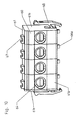
- FIGS. 1 and 2 show a first embodiment of the invention.
- FIG. 1 shows four terminals 10, each having a terminal housing 11 with a front side 11a, a back 11b, a top 11c, a bottom 11d and two side surfaces 11e.
- the terminals 10 are arranged side by side in a row.
- the terminal 10 has a clamping contact 15 with a clamping spring 15a.
- An unillustrated electrical conductor is through a third opening 14, which is like out FIG. 1 seen in the front 11 a of the terminal housing 11 of the terminal 10 is inserted into the interior of the terminal housing 11 and pushes the clamping spring 15 a against the spring force back until the electrical conductor between the clamping spring 15 a and the terminal contact 15 is fixed.
- a contact spring 16 is integrally arranged, wherein the contact spring 16 is guided through a first opening 12 of the terminal housing 11, which is arranged in the bottom 11 d of the terminal housing 11 to the outside of the terminal housing 11.
- the Contact spring 16 is designed as a leaf spring, wherein the contact spring 16 has a free end 16a, which protrudes through the first opening 12 of the terminal housing 11.
- FIG. 1 the free end 16a of the contact spring 16 when placing the terminal 10 on a circuit board 20 with a arranged on the circuit board 20 contact surface 22 into contact. Only by placing the terminal 10 on the circuit board 20 thus an electrically conductive contact between the contact spring 16, in particular its free end 16 a, and the contact surface 22 of the circuit board 20 is produced. In order to reduce the friction between the free end 16a of the contact spring 16 and the contact surface 22 of the circuit board 20, the free end 16a of the contact spring 16 is bent, in particular U-shaped.
- the contact surfaces 22 are preferably made of gold or tinned.
- the terminal 10 has an actuating element 17, which is accessible through a second opening 13 of the terminal housing 11 from the outside of the terminal housing 11.
- the actuating element 17 is designed in such a way that it can deflect the clamping spring 15a of the clamping contact 15 against the spring force of the clamping spring 15a in such a way that an electrical conductor clamped between the clamping spring 15a and the clamping contact 15 is released and can be withdrawn again from the terminal housing 11.
- two locking elements 18 are further arranged, with which the terminal 10 can engage in a housing, not shown, to fix the terminal 10 in position.
- the latching elements 18 it would also be possible to attach the latching elements 18 in such a way that the connection terminal 10 on the printed circuit board 20 can be latched over them.
- the locking elements 18 on each of the side surfaces, d. H. the front side 11a, the back 11b, the top 11c, the bottom 11d and / or the two side surfaces 11e of the terminal housing 11 are attached.
- FIG. 3 shows a terminal 10 ', which differs from the in the FIGS. 1 and 2 illustrated terminal 10 only slightly different. The same components are therefore designated by the same reference numerals.
- the terminal 10 ' has a clamping contact 15' with a clamping spring 15a ', wherein an electrical conductor, not shown, in turn between the clamping spring 15a' and the clamping contact 15 'can be clamped.
- the terminal 10 ' has a contact spring 16', which is connected by welding to the terminal contact 15 '.
- the contact spring 16 ' is formed as a leaf spring, which has a free end 16a', which is guided through the first opening 12 of the terminal housing 11 to the outside of the terminal housing 11, wherein the free end 16a 'in turn U-shaped bent ,
- the terminal 10 'thus differs only in the manner of attachment of the contact spring 16' to the terminal contact 15 'of the terminal 10 according to FIG. 1 and 2 ,
- FIGS. 4 and 5 show a third embodiment of the invention.
- FIG. 4 shows four terminals 30, each having a terminal housing 31 with a front 31a, a back 31b, a top 31c, a bottom 31d and two side surfaces 31e.
- the terminals 30 are arranged side by side in a row.
- connection terminal 30 has a clamping contact 35 with a clamping spring 35a.
- An electrical conductor not shown is inserted through a third opening which is located in the front 31a of the terminal housing 31 of the terminal 30 in the interior of the terminal housing 31 and thereby pushes the spring 35a against the spring force back until the electrical conductor between the Clamping spring 35a and the clamping contact 35 is fixed.
- a contact spring 36 is integrally arranged, wherein the contact spring 36 is guided through a first opening 32 of the terminal housing 31, which is arranged in the back 31 b of the terminal housing 31, on the outside of the terminal housing 31.
- the contact spring 36 is formed as a leaf spring, wherein the contact spring 36 has a free end 36 a, which protrudes through the first opening 32 of the terminal housing 31.
- the free end 36a of the contact spring 36 can analogously to the embodiment according to FIG. 1 when placing the terminal 30 on a printed circuit board, not shown, come into contact with a arranged on the circuit board contact surface.
- the free end 36a of the contact spring 36 is bent, in particular U-shaped.
- connection terminal 30 has an actuating element 37 which is accessible from the outside of the connection terminal housing 31 through a second opening 33 of the connection terminal housing 31.
- the actuating element 37 is configured such that it can deflect the clamping spring 35a of the clamping contact 35 against the spring force of the clamping spring 35a such that an electrical conductor clamped between the clamping spring 35a and the clamping contact 35 is released and can be withdrawn again from the terminal housing 31.
- the first opening 32 is arranged on the rear side 31 b of the terminal housing 31, while the second opening 33 is arranged on the underside 31 d of the terminal housing 31.
- two locking elements 38 are further arranged, with which the terminal 30 can engage in a housing, not shown, to fix the terminal 30 in position.
- the latching elements 38 it would also be possible to attach the latching elements 38 in such a way that the connection terminal 30 can be latched on the circuit board via them.
- the locking elements 38 can in particular be attached to each of the side surfaces, ie the front side 31a, the rear side 31b, the upper side 31c, the lower side 31d and / or the two side surfaces 31e of the terminal housing 31.
- FIGS. 6 and 7 show a fourth embodiment of the invention.
- FIG. 6 shows three terminals 40, each having a terminal housing 41 with a front side 41a, a back 41b, a top 41c, a bottom 41d and two side surfaces 41e.
- the terminals 40 are arranged side by side in a row.
- the terminal 40 has a screw 45, in which by means of a trained as a screw actuator 47, a clamping spring 45a against an electrical conductor, not shown, which is inserted through a third opening 44 in the interior of the terminal 40 is pressed.
- a clamping spring 45a against an electrical conductor, not shown, which is inserted through a third opening 44 in the interior of the terminal 40 is pressed.
- the screw 47 is accessible by a second opening 43, which is arranged in the bottom 41 d of the terminal housing 41 for a user and can be tightened or loosened, depending on whether an electrical conductor is to be clamped or withdrawn from the terminal housing 41 again ,
- a contact spring 46 is integrally arranged, wherein the contact spring 46 is guided through a first opening 42 of the terminal housing 41, which is arranged in the bottom 41d of the terminal housing 41 to the outside of the terminal housing 41.
- the contact spring 46 is formed as a leaf spring, wherein the contact spring 46 has a free end 46 a, which protrudes through the first opening 42 of the terminal housing 41.
- the terminal housing 41 further two locking elements 48 are further arranged, with which the terminal 40 can engage in a housing, not shown, to fix the terminal 40 in position.
- the latching elements 48 it would also be possible to attach the latching elements 48 in such a way that the connection terminal 40 can be latched on the circuit board via them.
- the locking elements 38 can in particular on each of the side surfaces, d. H. the front side 31 a, the back side 31 b, the top side 31 c, the bottom side 31 d, and / or the both side surfaces 31 e of the terminal housing 31 are attached.
- FIGS. 8 and 9 show the arrangement of the terminal 10 'according to FIG. 3 in a housing 50.
- the housing 50 has a first part 51 and a second part 52, wherein in the first part 51 in a recess 51b a plurality of terminals 10 'are held detenting about their locking elements 18.
- a circuit board 55 is arranged, which has on the terminals 10 'side facing corresponding contact surfaces on which the free ends 16a' of the contact springs 16 'of the terminals 10' are intended to rest.
- the corresponding leads for the terminals 10 ' are guided through an opening 51a in the first part 51 in the housing 50 and through the third openings 14 of the terminals 10' in the terminal contacts 15 'of the terminals 10', where they by the clamping springs 15a ' be held clamped.
- connection terminals 10 'and the circuit board 55 are shown positioned against each other so that the free end 16' of the terminals 10 'come to lie on the associated contact surfaces of the circuit board 55.
- the positioning is such that the terminals 10 'are pressed with a sufficiently high pressure against the circuit board 55, so that the system of the free ends 16a' of the contact springs 16 'is ensured at the contact surfaces of the circuit board 55.
- the terminals 10 'and the circuit board 55 are protected from external influences.
- FIG. 10 shows a fifth embodiment, four terminals 60, each having a terminal housing 61 having a front side 61a, a back, a top, a bottom and two side surfaces 61e, wherein the four terminals 60 are strung together over their mutually facing side surfaces 61e.
- a third opening 64 is arranged through which an unillustrated electrical conductor can be inserted into the terminal 60.
- the internal structure of the terminals 60 may be performed analogously to one of the previous embodiments. How out FIG. 10 can be seen, the connection terminals 60, for example, as an actuating element 67 on a pusher element, which has a function analogous to the actuating element 17 of the first embodiment.
- the two outer terminals 60 have at their respective outer side surface 61 e each have a locking element 68, via which the series of terminals 60 can be held in a housing, not shown, or on a printed circuit board, not shown detent.
- FIG. 11 6 shows a sixth exemplary embodiment of four connection terminals 70, each of which has a terminal housing 71 with a front side 71a, a rear side, an upper side, a lower side and two side surfaces 71e, wherein the four connection terminals 70 are arranged next to one another via their mutually facing side surfaces 71e.
- a third opening 74 is arranged, through which an unillustrated electrical conductor can be inserted into the terminal 70.
- the internal structure of the terminals 70 may be performed analogously to one of the previous embodiments. How out FIG. 11 can be seen, the connecting terminals 70, for example, as an actuating element 77 on a pusher element, which has a function analogous to the actuating element 17 of the first embodiment.
- these terminals 70 can not via locking elements 68, but arranged on the outer side surfaces 71a of the terminal housing 71 screw elements 78 in analog Way can be attached to a housing or a printed circuit board, not shown.
Abstract
Description
Die Erfindung betrifft eine Anschlussklemme gemäß dem Oberbegriff des Patentanspruchs 1.The invention relates to a terminal according to the preamble of patent claim 1.
Bekannt sind Anschlussklemmen mit einem isolierenden Anschlussklemmengehäuse und einem in dem Anschlussklemmengehäuse angeordneten Klemmkontakt zum Anschließen eines elektrischen Leiters. Eine derartige Anschlussklemme ist beispielsweise der
Alternativ sind auch oberflächenmontierbare Stifte bekannt, die auf eine Kontaktfläche der Leiterplatte beispielsweise durch Verlöten aufgebracht werden. Auf die Stifte werden wiederum die Anschlussklemmen mit einem entsprechenden Kontakt aufgebracht.Alternatively, surface-mountable pins are known which are applied to a contact surface of the printed circuit board, for example by soldering. In turn, the terminals are applied with a corresponding contact on the pins.
Nachteilig dabei ist, dass grundsätzlich separate Stifte zur Herstellung des Kontakts zwischen den Anschlussklemmen und den Leiterplatten benötigt werden. Zudem ist ein großer Montageaufwand nötig, die Stifte entweder in Durchlochtechnik oder in SMD(surface mounted device)-Technik auf der Leiterplatte zu befestigen und die Anschlussklemme anschließend auf die Stifte aufzubringen.The disadvantage here is that in principle separate pins for the production of the contact between the terminals and the circuit boards are needed. In addition, a large installation effort is necessary, the pins either in through hole technology or in SMD (surface mounted device) technology on the circuit board then attach the terminal to the pins.
Die Aufgabe der Erfindung besteht daher darin, eine Anschlussklemme bereitzustellen, bei welcher auf einfachere Art und Weise der elektrische Kontakt mit der Leiterplatte herstellbar ist.The object of the invention is to provide a terminal in which in a simpler manner, the electrical contact with the circuit board can be produced.
Die Aufgabe wird gelöst durch eine Anschlussklemme mit den Merkmalen des Patentanspruchs 1.The object is achieved by a terminal with the features of claim 1.
Vorteilhafte Ausgestaltungen und Weiterbildungen der Erfindung sind in den Unteransprüchen angegeben.Advantageous embodiments and further developments of the invention are specified in the subclaims.
Die Erfindung beruht auf dem Grundgedanken, eine direkte Kontaktierung zwischen der Anschlussklemme und einer leitfähigen Kontaktfläche auf der Oberfläche der Leiterplatte herzustellen anstatt wie gemäß dem Stand der Technik einen Kontaktstift, welcher auf der Leiterplatte angeordnet ist, zu kontaktieren. Erfindungsgemäß ist dazu eine Kontaktfeder vorgesehen, welche in dem Anschlussklemmengehäuse mit dem Klemmkontakt der Anschlussklemme in elektrisch leitender Verbindung steht und welche durch eine erste Öffnung des Anschlussklemmengehäuses auf die Außenseite des Anschlussklemmengehäuses geführt ist. Dabei ist die Kontaktfeder derart ausgebildet, dass sie bei Aufsetzen der Anschlussklemme auf eine Leiterplatte gegen eine Kontaktfläche der Leiterplatte drückt, um einen elektrischen Kontakt zwischen der Leiterplatte und dem Klemmkontakt herzustellen. Auf die separaten Kontaktstifte kann damit vollständig verzichtet werden. Dadurch werden neben den Kosten für die Stifte auch die Kosten für die Montage der Stifte eingespart.The invention is based on the idea to establish a direct contact between the terminal and a conductive contact surface on the surface of the circuit board instead of contacting as in the prior art, a contact pin, which is arranged on the circuit board. According to the invention, a contact spring is provided for this purpose, which is in the terminal housing with the terminal contact of the terminal in electrically conductive connection and which is guided through a first opening of the terminal housing on the outside of the terminal housing. In this case, the contact spring is designed such that it presses when placing the terminal on a circuit board against a contact surface of the circuit board to make electrical contact between the circuit board and the terminal contact. On the separate pins can thus be completely dispensed with. As a result, in addition to the cost of the pins and the cost of mounting the pins can be saved.
Vorzugsweise ist die Kontaktfeder als Blattfeder ausgebildet, welche sich besonders kostengünstig herstellen lässt.Preferably, the contact spring is designed as a leaf spring, which can be produced particularly inexpensively.
Gemäß einer besonders bevorzugten Ausführungsform der Erfindung ist das freie Ende der Blattfeder gebogen, insbesondere u-förmig gebogen. Durch ein derartiges Abbiegen des freien Endes der Blattfeder kann eine geringere Reibung zwischen der Blattfeder und der Kontaktfläche der Leiterplatte erreicht werden als in dem Fall, dass das freie Ende der Blattfeder an der Kontaktfläche der Leiterplatte anliegt. Zudem ist auch bei verschiedenen relativen Lagen zwischen der Kontaktfeder und der Kontaktfläche eine Anlagefläche und somit ein sicherer elektrischer Kontakt gewährleistet.According to a particularly preferred embodiment of the invention, the free end of the leaf spring is bent, in particular bent in a U-shape. By such bending of the free end of the leaf spring, a lower friction between the leaf spring and the contact surface of the circuit board can be achieved than in the case that the free end of the leaf spring rests against the contact surface of the circuit board. In addition, a contact surface and thus a secure electrical contact is ensured even at different relative positions between the contact spring and the contact surface.
In einer bevorzugten Ausführungsform der Erfindung ist die Kontaktfeder einstückig mit dem Klemmkontakt verbunden, um so den Herstellungsprozess von Kontaktfeder und Klemmkontakt zu vereinfachen.In a preferred embodiment of the invention, the contact spring is integrally connected to the terminal contact, so as to simplify the manufacturing process of contact spring and terminal contact.
In einer alternativen Ausführungsform der Erfindung ist die Kontaktfeder mit dem Klemmkontakt durch Nieten, Schweißen. Löten oder Verpressen verbunden, um beispielsweise auf diese Art und Weise unterschiedliche Materialien für Kontaktfeder und Klemmkontakt verwenden zu können.In an alternative embodiment of the invention, the contact spring with the clamping contact by riveting, welding. Soldering or pressing connected, for example, to be able to use different materials for contact spring and terminal contact in this way.
Der Klemmkontakt ist zum einfachen Anschließen eines elektrischen Leiters vorzugsweise als Schraubkontakt oder als Federklemmkontakt ausgebildet.The terminal contact is preferably designed for easy connection of an electrical conductor as a screw or as a spring terminal.
Gemäß einer besonders bevorzugten Ausführungsform der Erfindung weist der Klemmkontakt ein Betätigungselement zum Lösen des Klemmkontakts auf, wobei das Betätigungselement insbesondere durch eine zweite Öffnung in dem Anschlussklemmengehäuse zugänglich ist oder geführt ist. Ist der Klemmkontakt beispielsweise als Schraubkontakt ausgebildet, ist das Betätigungselement vorzugsweise als Schraube ausgebildet, die durch die zweite Öffnung in dem Anschlussklemmengehäuse zugänglich ist und somit auch nachträglich wieder gelöst werden kann, um den elektrischen Leiter wieder zu entfernen. Bei Ausbildung des Klemmkontakts als Federklemmkontakt kann das Betätigungselement beispielsweise als Drückerelement ausgebildet sein, welches gegen die Federkraft des Federklemmkontakts die Klemmfeder derart öffnen kann, dass der elektrische Leiter freigegeben wird und aus der Anschlussklemme wieder abgezogen werden kann. Dieses Drückerelement ist dabei vorzugsweise durch die zweite Öffnung in dem Anschlussklemmengehäuse nach außen geführt, um einfach zugänglich zu sein und von der Außenseite her betätigt werden zu können.According to a particularly preferred embodiment of the invention, the clamping contact on an actuating element for releasing the clamping contact, wherein the actuating element in particular by a second opening in the terminal housing is accessible or guided. If the terminal contact is formed, for example, as a screw contact, the actuating element is preferably designed as a screw which is accessible through the second opening in the terminal housing and thus can be subsequently released again to remove the electrical conductor again. When forming the terminal contact as a spring terminal contact, the actuating element may be formed, for example, as a pusher element which can open against the spring force of the spring terminal contact the clamping spring such that the electrical conductor is released and can be removed from the terminal again. This pusher element is preferably guided through the second opening in the terminal housing to the outside, to be easily accessible and to be operated from the outside can.
Bei einer vorteilhaften Ausgestaltung der Erfindung liegen die erste Öffnung und die zweite Öffnung in derselben Seite des Anschlussklemmengehäuses, um eine gute Zugangsmöglichkeit gewährleisten zu können.In an advantageous embodiment of the invention, the first opening and the second opening in the same side of the terminal housing, in order to ensure a good accessibility can.
Vorzugsweise ist an dem Anschlussklemmengehäuse wenigstens ein Verbindungselement, insbesondere wenigstens ein Rastelement und/oder wenigstens ein Schraubkontakt, zur Montage der Anschlussklemme auf der Leiterplatte und /oder in einem Gehäuse angeordnet. Ein Verbindungselement zur Montage der Anschlussklemme auf der Leiterplatte und/oder in einem Gehäuse ist insbesondere aus dem Grund bevorzugt, dass die Anschlussklemmen auf der Leiterplatte und/oder in dem Gehäuse fixiert werden können und ggf. der nötige Druck zur Herstellung des elektrischen Kontakts zwischen der Kontaktfläche der Leiterplatte und der Kontaktfeder der Anschlussklemme hergestellt und auch bei Bewegung der Leiterplatte und/oder des Gehäuses dauerhaft gewährleistet werden kann.Preferably, at least one connecting element, in particular at least one latching element and / or at least one screwed contact, for mounting the connecting terminal on the printed circuit board and / or in a housing is arranged on the terminal housing. A connecting element for mounting the connecting terminal on the printed circuit board and / or in a housing is particularly preferred for the reason that the terminals can be fixed on the circuit board and / or in the housing and possibly the pressure required to establish the electrical contact between the Contact surface of the circuit board and the contact spring of the terminal manufactured and also at Movement of the circuit board and / or the housing can be permanently ensured.
Vorzugsweise ist die Anschlussklemme anreihbar, um mehrere Anschlussklemmen platzsparend anordnen zu können, um die nötigen Anschlussklemmen für ein elektrisches oder elektronisches Gerät bereitzustellen.Preferably, the terminal can be arranged in rows in order to arrange several terminals space-saving to provide the necessary terminals for an electrical or electronic device.
Die erfindungsgemäße Anschlussklemme kommt insbesondere in einem Gehäuse mit einem ersten Teil und einem zweiten Teil zum Einsatz, wobei in dem ersten Teil wenigstens eine erfindungsgemäße Anschlussklemme und in dem zweiten Teil eine Leiterplatte mit wenigstens einer Kontaktfläche angeordnet ist, wobei bei Zusammenfügen des ersten Teils und des zweiten Teils die Kontaktfeder der Anschlussklemme gegen die entsprechende Kontaktfläche der Leiterplatte gedrückt wird, um einen elektrisch leitenden Kontakt herzustellen. Auf diese Art und Weise wird einerseits der elektrisch leitende Kontakt zwischen der Kontaktfläche und der Anschlussklemme bei Zusammenbau des Gehäuses gewährleistet und zudem die Anschlussklemme und die Leiterplatte gegen Außeneinflüsse geschützt.The terminal according to the invention is used in particular in a housing having a first part and a second part, wherein in the first part at least one terminal according to the invention and in the second part of a printed circuit board is arranged with at least one contact surface, wherein upon assembly of the first part and the second part, the contact spring of the terminal is pressed against the corresponding contact surface of the printed circuit board to produce an electrically conductive contact. In this way, on the one hand the electrically conductive contact between the contact surface and the terminal is ensured during assembly of the housing and also protected the terminal and the circuit board against external influences.
Vorzugsweise sind der erste Teil und der zweite Teil des Gehäuses über eine Rastverbindung miteinander verbunden, welche besonders einfach herzustellen und zu montieren ist.Preferably, the first part and the second part of the housing are connected to one another via a latching connection, which is particularly easy to manufacture and assemble.
Besonders bevorzugt sind in dem ersten Teil mehrere Anschlussklemmen und auf der Leiterplatte mehrere entsprechende Kontaktflächen angeordnet, um für ein elektronisches Gerät alle nötigen Anschlüsse auf einfache Art und Weise bereitstellen und montieren zu können.More preferably, a plurality of terminals are arranged in the first part and on the circuit board a plurality of corresponding contact surfaces in order to provide and mount all the necessary connections for an electronic device in a simple manner.
Um einen guten elektrischen Kontakt zwischen den Kontaktflächen der Leiterplatte und den Kontaktfedern der Anschlussklemmen gewährleisten zu können, sind vorzugsweise die Kontaktflächen der Leiterplatte vergoldet oder verzinnt.In order to ensure a good electrical contact between the contact surfaces of the circuit board and the contact springs of the terminals, preferably the contact surfaces of the circuit board are gold plated or tinned.
Die Erfindung wird anhand der folgenden Figuren ausführlich erläutert.The invention will be explained in detail with reference to the following figures.
- Figur 1FIG. 1
- eine perspektivische Ansicht eines ersten Ausführungsbeispiels der Erfindung,a perspective view of a first embodiment of the invention,
- Figur 2FIG. 2
-
einen Schnitt durch eine Anschlussklemme des Ausführungsbeispiels gemäß
Figur 1 ,a section through a terminal of the embodiment according toFIG. 1 . - Figur 3FIG. 3
- einen Schnitt durch ein zweites Ausführungs- beispiel der Erfindung,a section through a second embodiment of the invention,
- Figur 4FIG. 4
- eine perspektivische Ansicht eines dritten Ausführungsbeispiels der Erfindung,a perspective view of a third embodiment of the invention,
- Figur 5FIG. 5
-
einen Schnitt durch eine Anschlussklemme des Ausführungsbeispiels gemäß
Figur 4 ,a section through a terminal of the embodiment according toFIG. 4 . - Figur 6FIG. 6
- eine perspektivische Ansicht eines vierten Ausführungsbeispiels der Erfindung,a perspective view of a fourth embodiment of the invention,
- Figur 7FIG. 7
-
einen Schnitt durch eine Anschlussklemme des Ausführungsbeispiels gemäß
Figur 6 ,a section through a terminal of the embodiment according toFIG. 6 . - Figur 8FIG. 8
-
eine perspektivische Ansicht einer Anordnung von Anschlussklemmen gemäß
Figur 3 in einem Gehäuse, wobei das Gehäuse geöffnet ist,a perspective view of an arrangement of terminals according toFIG. 3 in a housing, wherein the housing is open, - Figur 9FIG. 9
-
das Gehäuse gemäß
Figur 8 in zusammengesetztem Zustand,the housing according toFIG. 8 in assembled condition, - Figur 10FIG. 10
- eine perspektivische Ansicht eines fünften Ausführungsbeispiels der Erfindung unda perspective view of a fifth embodiment of the invention and
- Figur 11FIG. 11
- eine perspektivische Ansicht eines sechsten Ausführungsbeispiels der Erfindung.a perspective view of a sixth embodiment of the invention.
Die
Wie aus
An dem Klemmkontakt 15 ist einstückig eine Kontaktfeder 16 angeordnet, wobei die Kontaktfeder 16 durch eine erste Öffnung 12 des Anschlussklemmengehäuses 11, welche in der Unterseite 11d des Anschlussklemmengehäuses 11 angeordnet ist, auf die Außenseite des Anschlussklemmengehäuses 11 geführt ist. Die Kontaktfeder 16 ist dabei als Blattfeder ausgebildet, wobei die Kontaktfeder 16 ein freies Ende 16a aufweist, das durch die erste Öffnung 12 aus dem Anschlussklemmengehäuse 11 herausragt.On the
Wie aus
Um einen besonders guten elektrischen Kontakt zwischen den freien Enden 16a und den Kontaktflächen 22 der Leiterplatte 20 gewährleisten zu können, sind die Kontaktflächen 22 vorzugsweise vergoldet oder verzinnt ausgeführt.In order to ensure a particularly good electrical contact between the free ends 16a and the contact surfaces 22 of the
Die Anschlussklemme 10 weist ein Betätigungselement 17 auf, welches durch eine zweite Öffnung 13 des Anschlussklemmengehäuses 11 von der Außenseite des Anschlussklemmengehäuses 11 zugänglich ist. Das Betätigungselement 17 ist derart ausgebildet, dass es die Klemmfeder 15a des Klemmkontakts 15 gegen die Federkraft der Klemmfeder 15a derart auslenken kann, dass ein zwischen der Klemmfeder 15a und dem Klemmkontakt 15 geklemmter elektrischer Leiter freigegeben wird und wieder aus dem Anschlussklemmengehäuse 11 abgezogen werden kann.The terminal 10 has an
An dem Anschlussklemmengehäuse 11 sind weiterhin jeweils zwei Rastelemente 18 angeordnet, mit welchen die Anschlussklemme 10 in einem nicht dargestellten Gehäuse einrasten kann, um die Anschlussklemme 10 in ihrer Position zu fixieren. Grundsätzlich wäre es auch möglich, die Rastelemente 18 derart anzubringen, dass über sie die Anschlussklemme 10 auf der Leiterplatte 20 rastend gehalten werden kann. Selbstverständlich können die Rastelemente 18 an jeder der Seitenflächen, d. h. der Vorderseite 11a, der Rückseite 11b, der Oberseite 11c, der Unterseite 11d und/oder den beiden Seitenflächen 11e des Anschlussklemmengehäuses 11 angebracht werden.At the
In
Die
Wie aus
An dem Klemmkontakt 35 ist einstückig eine Kontaktfeder 36 angeordnet, wobei die Kontaktfeder 36 durch eine erste Öffnung 32 des Anschlussklemmengehäuses 31, welche in der Rückseite 31b des Anschlussklemmengehäuses 31 angeordnet ist, auf die Außenseite des Anschlussklemmengehäuses 31 geführt. Die Kontaktfeder 36 ist dabei als Blattfeder ausgebildet, wobei die Kontaktfeder 36 ein freies Ende 36a aufweist, das durch die erste Öffnung 32 aus dem Anschlussklemmengehäuse 31 herausragt. Das freie Ende 36a der Kontaktfeder 36 kann analog zum Ausführungsbeispiel gemäß
Die Anschlussklemme 30 weist ein Betätigungselement 37 auf, welches durch eine zweite Öffnung 33 des Anschlussklemmengehäuses 31 von der Außenseite des Anschlussklemmengehäuses 31 zugänglich ist. Das Betätigungselement 37 ist derart ausgebildet, dass es die Klemmfeder 35a des Klemmkontakts 35 gegen die Federkraft der Klemmfeder 35a derart auslenken kann, dass ein zwischen der Klemmfeder 35a und dem Klemmkontakt 35 geklemmter elektrischer Leiter freigegeben wird und wieder aus dem Anschlussklemmengehäuse 31 abgezogen werden kann.The
Die erste Öffnung 32 ist auf der Rückseite 31b des Anschlussklemmengehäuses 31 angeordnet, während die zweite Öffnung 33 auf der Unterseite 31d des Anschlussklemmengehäuses 31 angeordnet ist. Je nachdem, wie die Anschlussklemmengehäuse 31 in einem nicht dargestellten Gehäuse positioniert werden, kann es von Vorteil sein, das freie Ende 36a der Kontaktfeder 36 auf entsprechenden Seiten 31a, 31b, 31c, 31d des Anschlussklemmengehäuses 31 herauszuführen.The
An dem Anschlussklemmengehäuse 31 sind weiterhin jeweils zwei Rastelemente 38 angeordnet, mit welchen die Anschlussklemme 30 in einem nicht dargestellten Gehäuse einrasten kann, um die Anschlussklemme 30 in ihrer Position zu fixieren. Grundsätzlich wäre es auch möglich, die Rastelemente 38 derart anzubringen, dass über sie die Anschlussklemme 30 auf der Leiterplatte rastend gehalten werden kann. Die Rastelemente 38 können insbesondere an jeder der Seitenflächen, d. h. der Vorderseite 31a, der Rückseite 31b, der Oberseite 31c, der Unterseite 31d und/oder den beiden Seitenflächen 31e des Anschlussklemmengehäuses 31 angebracht werden.On the
Die
Wie aus
An dem Klemmkontakt 45 ist einstückig eine Kontaktfeder 46 angeordnet, wobei die Kontaktfeder 46 durch eine erste Öffnung 42 des Anschlussklemmengehäuses 41, welche in der Unterseite 41d des Anschlussklemmengehäuses 41 angeordnet ist, auf die Außenseite des Anschlussklemmengehäuses 41 geführt ist. Die Kontaktfeder 46 ist dabei als Blattfeder ausgebildet, wobei die Kontaktfeder 46 ein freies Ende 46a aufweist, das durch die erste Öffnung 42 aus dem Anschlussklemmengehäuse 41 herausragt. Bei Aufsetzen der Anschlussklemme 40 auf eine Leiterplatte kann das freie Ende 46a der Kontaktfeder 46 in elektrisch leitenden Kontakt mit Kontaktflächen der Leiterplatte kommen. Um die Reibung zwischen dem freien Ende 46a der Kontaktfeder 46 und der Kontaktfläche 22 der Leiterplatte 20 zu verringern, ist das freie Ende 46a der Kontaktfeder 46 gebogen, insbesondere u-förmig ausgebildet.On the clamping
An dem Anschlussklemmengehäuse 41 sind weiterhin jeweils zwei Rastelemente 48 angeordnet, mit welchen die Anschlussklemme 40 in einem nicht dargestellten Gehäuse einrasten kann, um die Anschlussklemme 40 in ihrer Position zu fixieren. Grundsätzlich wäre es auch möglich, die Rastelemente 48 derart anzubringen, dass über sie die Anschlussklemme 40 auf der Leiterplatte rastend gehalten werden kann. Die Rastelemente 38 können insbesondere an jeder der Seitenflächen, d. h. der Vorderseite 31a, der Rückseite 31b, der Oberseite 31c, der Unterseite 31d und/oder den beiden Seitenflächen 31e des Anschlussklemmengehäuses 31 angebracht werden.On the
Die
Bei Aufsetzen des zweiten Teils 52 auf das erste Teil 51 wie in
Die beiden äußeren Anschlussklemmen 60 weisen an ihrer jeweiligen äußeren Seitenfläche 61e jeweils ein Rastelement 68 auf, über welches die Reihe der Anschlussklemmen 60 in einem nicht dargestellten Gehäuse oder auf einer nicht dargestellten Leiterplatte rastend gehalten werden kann.The two
Durch eine nicht dargestellte Öffnung der Anschlussklemmengehäuse 61 der Anschlussklemmen 60 ragt, wie in
Im Gegensatz zu dem in
Durch eine nicht dargestellte Öffnung der Anschlussklemmengehäuse 71 der Anschlussklemmen 60 ragt, wie in
- 1010
- Anschlussklemmeterminal
- 1111
- AnschlussklemmengehäuseTerminal housing
- 11a11a
- Vorderseitefront
- 11b11b
- Rückseiteback
- 11c11c
- Oberseitetop
- 11d11d
- Unterseitebottom
- 11e11e
- Seitenflächeside surface
- 1212
- erste Öffnungfirst opening
- 1313
- zweite Öffnungsecond opening
- 1414
- dritte Öffnungthird opening
- 1515
- Klemmkontaktclamping contact
- 15a15a
- Klemmfederclamping spring
- 1616
- Kontaktfedercontact spring
- 16a16a
- freies Endefree end
- 1717
- Betätigungselementactuator
- 1818
- Rastelementlocking element
- 10'10 '
- Anschlussklemmeterminal
- 15'15 '
- Klemmkontaktclamping contact
- 15a'15a '
- Klemmfederclamping spring
- 16'16 '
- Kontaktfedercontact spring
- 16a'16a '
- freies Endefree end
- 2020
- Leiterplattecircuit board
- 2222
- Kontaktflächecontact area
- 3030
- Anschlussklemmeterminal
- 3131
- AnschlussklemmengehäuseTerminal housing
- 31a31a
- Vorderseitefront
- 31b31b
- Rückseiteback
- 31c31c
- Oberseitetop
- 31d31d
- Unterseitebottom
- 31e31e
- Seitenflächeside surface
- 3232
- erste Öffnungfirst opening
- 3333
- zweite Öffnungsecond opening
- 3535
- Klemmkontaktclamping contact
- 35a35a
- Klemmfederclamping spring
- 3636
- Kontaktfedercontact spring
- 36a36a
- freies Endefree end
- 3737
- Betätigungselementactuator
- 3838
- Rastelementlocking element
- 4040
- Anschlussklemmeterminal
- 4141
- AnschlussklemmengehäuseTerminal housing
- 41a41a
- Vorderseitefront
- 41b41b
- Rückseiteback
- 41c41c
- Oberseitetop
- 41d41d
- Unterseitebottom
- 41e41e
- Seitenflächeside surface
- 4242
- erste Öffnungfirst opening
- 4343
- zweite Öffnungsecond opening
- 4444
- dritte Öffnungthird opening
- 4545
- Schraubkontaktbolted
- 45a45a
- Klemmfederclamping spring
- 4646
- Kontaktfedercontact spring
- 46a46a
- freies Endefree end
- 4747
- Schraubescrew
- 4848
- Rastelementlocking element
- 5050
- Gehäusecasing
- 5151
- erstes Teilfirst part
- 51a51a
- Öffnungopening
- 51b51b
- Ausnehmungrecess
- 5252
- zweites Teilsecond part
- 5555
- Leiterplattecircuit board
- 6060
- Anschlussklemmeterminal
- 6161
- AnschlussklemmengehäuseTerminal housing
- 61a61a
- Vorderseitefront
- 61e61e
- Seitenflächeside surface
- 6464
- dritte Öffnungthird opening
- 66a66a
- freies Endefree end
- 6767
- Betätigungselementactuator
- 6868
- Rastelementlocking element
- 7070
- Anschlussklemmeterminal
- 7171
- AnschlussklemmengehäuseTerminal housing
- 71a71a
- Vorderseitefront
- 71e71e
- Seitenflächeside surface
- 7474
- dritte Öffnungthird opening
- 7777
- Betätigungselementactuator
- 7878
- Schraubelementscrew
Claims (13)
dadurch gekennzeichnet, dass eine Kontaktfeder, welche in dem Anschlussklemmengehäuse mit dem Klemmkontakt in elektrisch leitender Verbindung steht, durch eine erste Öffnung des Anschlussklemmengehäuses auf die Außenseite des Anschlussklemmengehäuses geführt ist, wobei die Kontaktfeder derart ausgebildet ist, dass sie bei Aufsetzen der Anschlussklemme auf eine Leiterplatte gegen eine Kontaktfläche der Leiterplatte drückt, um einen elektrischen Kontakt zwischen der Leiterplatte und dem Klemmkontakt herzustellen.Terminal block with an insulating terminal housing and a clamping contact arranged in the terminal housing for connecting an electrical conductor,
characterized in that a contact spring, which is in the terminal housing with the terminal contact in electrically conductive connection, is guided through a first opening of the terminal housing on the outside of the terminal housing, wherein the contact spring is designed such that when placing the terminal on a circuit board presses against a contact surface of the circuit board to make electrical contact between the circuit board and the terminal contact.
dadurch gekennzeichnet, dass die Kontaktfeder als Blattfeder ausgebildet ist.Terminal according to claim 1,
characterized in that the contact spring is designed as a leaf spring.
dadurch gekennzeichnet, dass das freie Ende der Blattfeder gebogen ist, insbesondere u-förmig gebogen ist.Terminal according to claim 2,
characterized in that the free end of the leaf spring is bent, in particular bent in a U-shape.
dadurch gekennzeichnet, dass die Kontaktfeder einstückig mit dem Klemmkontakt verbunden ist.Terminal according to one of the preceding claims,
characterized in that the contact spring is integrally connected to the terminal contact.
dadurch gekennzeichnet, dass die Kontaktfeder mit dem Klemmkontakt durch Nieten, Schweißen, Löten oder Verpressen verbunden ist.Terminal according to one of the preceding claims,
characterized in that the contact spring is connected to the terminal contact by riveting, welding, soldering or pressing.
dadurch gekennzeichnet, dass der Klemmkontakt als Schraubkontakt oder als Federklemmkontakt ausgebildet ist.Terminal according to one of the preceding claims,
characterized in that the clamping contact is designed as a screw or as a spring terminal contact.
dadurch gekennzeichnet, dass der Klemmkontakt ein Betätigungselement zum Lösen des Klemmkontakts aufweist, wobei das Betätigungselement durch eine zweite Öffnung in dem Anschlussklemmengehäuse zugänglich ist oder geführt ist.Terminal according to one of the preceding claims,
characterized in that the clamping contact comprises an actuating element for releasing the clamping contact, wherein the actuating element is accessible or guided by a second opening in the terminal housing.
dadurch gekennzeichnet, dass die erste Öffnung und die zweite Öffnung in derselben Seite des Anschlussklemmengehäuses liegen.Terminal according to claim 7,
characterized in that the first opening and the second opening are in the same side of the terminal housing.
dadurch gekennzeichnet, dass an dem Anschlussklemmengehäuse wenigstens ein Verbindungselement, insbesondere wenigstens ein Rastelement und/oder wenigstens ein Schraubkontakt, zur Montage der Anschlussklemme auf der Leiterplatte und/oder in einem Gehäuse angeordnet ist.Terminal according to one of the preceding claims,
characterized in that at least one connecting element, in particular at least one latching element and / or at least one screwed contact, for mounting the connecting terminal on the printed circuit board and / or in a housing is arranged on the terminal housing.
dadurch gekennzeichnet, dass der erste Teil und der zweite Teil über eine Rastverbindung miteinander verbunden sind.Housing according to claim 10,
characterized in that the first part and the second part are connected to one another via a latching connection.
dadurch gekennzeichnet, dass in dem ersten Teil mehrere Anschlussklemmen und auf der Leiterplatte mehrere entsprechende Kontaktflächen angeordnet sind.Housing according to claim 10 or 11,
characterized in that in the first part a plurality of terminals and on the circuit board a plurality of corresponding contact surfaces are arranged.
dadurch gekennzeichnet, dass die Kontaktflächen der Leiterplatte vergoldet oder verzinnt sind.Housing according to one of claims 10 to 12,
characterized in that the contact surfaces of the printed circuit board are gold plated or tinned.
Applications Claiming Priority (1)
| Application Number | Priority Date | Filing Date | Title |
|---|---|---|---|
| DE102007043197.1A DE102007043197B4 (en) | 2007-09-11 | 2007-09-11 | terminal |
Publications (3)
| Publication Number | Publication Date |
|---|---|
| EP2037536A2 true EP2037536A2 (en) | 2009-03-18 |
| EP2037536A3 EP2037536A3 (en) | 2010-06-30 |
| EP2037536B1 EP2037536B1 (en) | 2012-07-18 |
Family
ID=40111004
Family Applications (1)
| Application Number | Title | Priority Date | Filing Date |
|---|---|---|---|
| EP08013402A Active EP2037536B1 (en) | 2007-09-11 | 2008-07-25 | Connection terminal |
Country Status (3)
| Country | Link |
|---|---|
| US (1) | US7780460B2 (en) |
| EP (1) | EP2037536B1 (en) |
| DE (1) | DE102007043197B4 (en) |
Cited By (5)
| Publication number | Priority date | Publication date | Assignee | Title |
|---|---|---|---|---|
| WO2010124792A1 (en) * | 2009-04-27 | 2010-11-04 | Abb Ag | Installation switchgear and method for assembling the same |
| WO2012136536A1 (en) * | 2011-04-08 | 2012-10-11 | Ptr Messtechnik Gmbh & Co. Kommanditgesellschaft | Conductor terminal for two opposite printed circuit boards |
| EP2581990A3 (en) * | 2011-10-10 | 2014-10-08 | Televes, S.A. | Housing for a telecommunication device |
| EP3349306A1 (en) * | 2017-01-12 | 2018-07-18 | ABB Schweiz AG | Modular terminal block |
| IT201700015793A1 (en) * | 2017-02-14 | 2018-08-14 | Sauro S R L | CONNECTOR FOR PRINTED CIRCUIT BOARDS |
Families Citing this family (76)
| Publication number | Priority date | Publication date | Assignee | Title |
|---|---|---|---|---|
| US11026768B2 (en) | 1998-10-08 | 2021-06-08 | Align Technology, Inc. | Dental appliance reinforcement |
| US8738394B2 (en) | 2007-11-08 | 2014-05-27 | Eric E. Kuo | Clinical data file |
| US8108189B2 (en) | 2008-03-25 | 2012-01-31 | Align Technologies, Inc. | Reconstruction of non-visible part of tooth |
| US9492243B2 (en) | 2008-05-23 | 2016-11-15 | Align Technology, Inc. | Dental implant positioning |
| US8092215B2 (en) | 2008-05-23 | 2012-01-10 | Align Technology, Inc. | Smile designer |
| US8172569B2 (en) | 2008-06-12 | 2012-05-08 | Align Technology, Inc. | Dental appliance |
| US8152518B2 (en) | 2008-10-08 | 2012-04-10 | Align Technology, Inc. | Dental positioning appliance having metallic portion |
| US8292617B2 (en) | 2009-03-19 | 2012-10-23 | Align Technology, Inc. | Dental wire attachment |
| US8765031B2 (en) | 2009-08-13 | 2014-07-01 | Align Technology, Inc. | Method of forming a dental appliance |
| US7909633B1 (en) * | 2009-09-15 | 2011-03-22 | Fisher-Rosemount Systems, Inc. | Wire connection apparatus |
| US9241774B2 (en) | 2010-04-30 | 2016-01-26 | Align Technology, Inc. | Patterned dental positioning appliance |
| US9211166B2 (en) | 2010-04-30 | 2015-12-15 | Align Technology, Inc. | Individualized orthodontic treatment index |
| DE102010046563B4 (en) | 2010-09-27 | 2018-05-03 | Mc Technology Gmbh | Terminal and terminal board assembly |
| US11211741B2 (en) * | 2011-06-03 | 2021-12-28 | Greatbatch Ltd. | Removable terminal pin connector for an active electronics circuit board for use in an implantable medical device |
| US9403238B2 (en) | 2011-09-21 | 2016-08-02 | Align Technology, Inc. | Laser cutting |
| US9375300B2 (en) | 2012-02-02 | 2016-06-28 | Align Technology, Inc. | Identifying forces on a tooth |
| US9220580B2 (en) | 2012-03-01 | 2015-12-29 | Align Technology, Inc. | Determining a dental treatment difficulty |
| US9414897B2 (en) | 2012-05-22 | 2016-08-16 | Align Technology, Inc. | Adjustment of tooth position in a virtual dental model |
| DE102012019229B4 (en) * | 2012-10-01 | 2022-09-29 | Phoenix Contact Gmbh & Co. Kg | PCB contacting system |
| US9263809B2 (en) | 2013-10-29 | 2016-02-16 | Corning Optical Communications Wireless Ltd | Terminal block |
| DE102014105725A1 (en) * | 2014-04-23 | 2015-10-29 | Wago Verwaltungsgesellschaft Mbh | Electrical device and conductor connection terminal and base part for this purpose |
| DE102014109143A1 (en) * | 2014-06-30 | 2015-12-31 | Phoenix Contact Gmbh & Co. Kg | PCB terminal |
| US10772506B2 (en) | 2014-07-07 | 2020-09-15 | Align Technology, Inc. | Apparatus for dental confocal imaging |
| US9675430B2 (en) | 2014-08-15 | 2017-06-13 | Align Technology, Inc. | Confocal imaging apparatus with curved focal surface |
| US9653861B2 (en) | 2014-09-17 | 2017-05-16 | Corning Optical Communications Wireless Ltd | Interconnection of hardware components |
| US10449016B2 (en) | 2014-09-19 | 2019-10-22 | Align Technology, Inc. | Arch adjustment appliance |
| US9610141B2 (en) | 2014-09-19 | 2017-04-04 | Align Technology, Inc. | Arch expanding appliance |
| DE102014114026B4 (en) * | 2014-09-26 | 2023-03-30 | Wago Verwaltungsgesellschaft Mbh | Conductor terminal and method of assembly |
| US9744001B2 (en) | 2014-11-13 | 2017-08-29 | Align Technology, Inc. | Dental appliance with cavity for an unerupted or erupting tooth |
| US10504386B2 (en) | 2015-01-27 | 2019-12-10 | Align Technology, Inc. | Training method and system for oral-cavity-imaging-and-modeling equipment |
| US9742079B2 (en) * | 2015-05-21 | 2017-08-22 | Cummins Inc. | Connector paint protection shield |
| DE102015113734A1 (en) | 2015-08-19 | 2017-02-23 | Wago Verwaltungsgesellschaft Mbh | Connectors |
| US10248883B2 (en) | 2015-08-20 | 2019-04-02 | Align Technology, Inc. | Photograph-based assessment of dental treatments and procedures |
| US11931222B2 (en) | 2015-11-12 | 2024-03-19 | Align Technology, Inc. | Dental attachment formation structures |
| US11554000B2 (en) | 2015-11-12 | 2023-01-17 | Align Technology, Inc. | Dental attachment formation structure |
| US11103330B2 (en) | 2015-12-09 | 2021-08-31 | Align Technology, Inc. | Dental attachment placement structure |
| US11596502B2 (en) | 2015-12-09 | 2023-03-07 | Align Technology, Inc. | Dental attachment placement structure |
| WO2017218947A1 (en) | 2016-06-17 | 2017-12-21 | Align Technology, Inc. | Intraoral appliances with sensing |
| US10383705B2 (en) | 2016-06-17 | 2019-08-20 | Align Technology, Inc. | Orthodontic appliance performance monitor |
| EP3490439B1 (en) | 2016-07-27 | 2023-06-07 | Align Technology, Inc. | Intraoral scanner with dental diagnostics capabilities |
| US10507087B2 (en) | 2016-07-27 | 2019-12-17 | Align Technology, Inc. | Methods and apparatuses for forming a three-dimensional volumetric model of a subject's teeth |
| DE102016120180B4 (en) | 2016-10-24 | 2019-04-04 | Phoenix Contact Gmbh & Co. Kg | PCB and multiple terminal |
| CN117257492A (en) | 2016-11-04 | 2023-12-22 | 阿莱恩技术有限公司 | Method and apparatus for dental imaging |
| WO2018102770A1 (en) | 2016-12-02 | 2018-06-07 | Align Technology, Inc. | Force control, stop mechanism, regulating structure of removable arch adjustment appliance |
| EP3547950A1 (en) | 2016-12-02 | 2019-10-09 | Align Technology, Inc. | Methods and apparatuses for customizing rapid palatal expanders using digital models |
| CN114224534A (en) | 2016-12-02 | 2022-03-25 | 阿莱恩技术有限公司 | Palatal expander and method of expanding a palate |
| US11026831B2 (en) | 2016-12-02 | 2021-06-08 | Align Technology, Inc. | Dental appliance features for speech enhancement |
| FR3060216B1 (en) * | 2016-12-09 | 2019-07-19 | Schneider Electric Industries Sas | ELECTRICAL CONNECTION TERMINAL BETWEEN TWO CONDUCTIVE ELEMENTS |
| US10548700B2 (en) | 2016-12-16 | 2020-02-04 | Align Technology, Inc. | Dental appliance etch template |
| US10456043B2 (en) | 2017-01-12 | 2019-10-29 | Align Technology, Inc. | Compact confocal dental scanning apparatus |
| US10779718B2 (en) | 2017-02-13 | 2020-09-22 | Align Technology, Inc. | Cheek retractor and mobile device holder |
| US10613515B2 (en) | 2017-03-31 | 2020-04-07 | Align Technology, Inc. | Orthodontic appliances including at least partially un-erupted teeth and method of forming them |
| US11045283B2 (en) | 2017-06-09 | 2021-06-29 | Align Technology, Inc. | Palatal expander with skeletal anchorage devices |
| WO2019005808A1 (en) | 2017-06-26 | 2019-01-03 | Align Technology, Inc. | Biosensor performance indicator for intraoral appliances |
| US10885521B2 (en) | 2017-07-17 | 2021-01-05 | Align Technology, Inc. | Method and apparatuses for interactive ordering of dental aligners |
| WO2019018784A1 (en) | 2017-07-21 | 2019-01-24 | Align Technology, Inc. | Palatal contour anchorage |
| CN115462921A (en) | 2017-07-27 | 2022-12-13 | 阿莱恩技术有限公司 | Tooth staining, transparency and glazing |
| EP4278957A3 (en) | 2017-07-27 | 2024-01-24 | Align Technology, Inc. | System and methods for processing an orthodontic aligner by means of an optical coherence tomography |
| US11116605B2 (en) | 2017-08-15 | 2021-09-14 | Align Technology, Inc. | Buccal corridor assessment and computation |
| US11123156B2 (en) | 2017-08-17 | 2021-09-21 | Align Technology, Inc. | Dental appliance compliance monitoring |
| US10813720B2 (en) | 2017-10-05 | 2020-10-27 | Align Technology, Inc. | Interproximal reduction templates |
| WO2019084326A1 (en) | 2017-10-27 | 2019-05-02 | Align Technology, Inc. | Alternative bite adjustment structures |
| EP3703608B1 (en) | 2017-10-31 | 2023-08-30 | Align Technology, Inc. | Determination of a dental appliance having selective occlusal loading and controlled intercuspation |
| WO2019089989A2 (en) | 2017-11-01 | 2019-05-09 | Align Technology, Inc. | Automatic treatment planning |
| WO2019100022A1 (en) | 2017-11-17 | 2019-05-23 | Align Technology, Inc. | Orthodontic retainers |
| EP3716885B1 (en) | 2017-11-30 | 2023-08-30 | Align Technology, Inc. | Orthodontic intraoral appliances comprising sensors |
| WO2019118876A1 (en) | 2017-12-15 | 2019-06-20 | Align Technology, Inc. | Closed loop adaptive orthodontic treatment methods and apparatuses |
| US10980613B2 (en) | 2017-12-29 | 2021-04-20 | Align Technology, Inc. | Augmented reality enhancements for dental practitioners |
| CN108281832A (en) * | 2018-01-25 | 2018-07-13 | 惠阳晋煜工业有限公司 | A kind of connector |
| ES2907213T3 (en) | 2018-01-26 | 2022-04-22 | Align Technology Inc | Diagnostic intraoral scanning and tracking |
| US11937991B2 (en) | 2018-03-27 | 2024-03-26 | Align Technology, Inc. | Dental attachment placement structure |
| CA3096417A1 (en) | 2018-04-11 | 2019-10-17 | Align Technology, Inc. | Releasable palatal expanders |
| DE102020115991B4 (en) | 2020-06-17 | 2022-06-09 | WAGO Verwaltungsgesellschaft mit beschränkter Haftung | Conductor connection terminal with actuation by a conductor connection module |
| JP7429905B2 (en) * | 2020-06-19 | 2024-02-09 | パナソニックIpマネジメント株式会社 | Wiring connection equipment and wiring equipment equipped with the same |
| DE102021129064A1 (en) | 2021-11-09 | 2023-05-11 | Metz Connect Tech Gmbh | PCB terminal block |
| DE102021129065A1 (en) | 2021-11-09 | 2023-05-11 | Metz Connect Tech Gmbh | PCB terminal block |
Citations (1)
| Publication number | Priority date | Publication date | Assignee | Title |
|---|---|---|---|---|
| DE4420984A1 (en) | 1994-06-10 | 1995-12-14 | Metz Albert Ria Electronic | Plug-and-socket connector with profiled grooves for encoding |
Family Cites Families (10)
| Publication number | Priority date | Publication date | Assignee | Title |
|---|---|---|---|---|
| CH656041A5 (en) * | 1982-06-23 | 1986-05-30 | Elektrowatt Ag | APPARATUS MOUNTED ON A COMMON RAIL. |
| US5494456A (en) * | 1994-10-03 | 1996-02-27 | Methode Electronics, Inc. | Wire-trap connector with anti-overstress member |
| DE19614988A1 (en) * | 1996-04-16 | 1997-10-23 | Tridonic Bauelemente | Electrical connector and connector for use in an electrical connector |
| US5729442A (en) * | 1996-05-31 | 1998-03-17 | The Whitaker Corporation | Thermostat housing with removable terminal block |
| JP3862870B2 (en) * | 1997-09-25 | 2006-12-27 | 北陸電気工業株式会社 | Electrical components with solderless terminal fittings |
| JP2000124012A (en) * | 1998-10-20 | 2000-04-28 | Hokuriku Electric Ind Co Ltd | Electric component and variable resistor for high voltage |
| US6074242A (en) * | 1998-12-31 | 2000-06-13 | Methode Electronics, Inc. | Wire-trap connector for solderless compression connection |
| DE10114921B4 (en) * | 2001-03-26 | 2016-08-18 | Wago Verwaltungsgesellschaft Mbh | Electrical. Spring terminal |
| EP1253670B1 (en) * | 2001-04-23 | 2006-04-26 | Weidmüller Interface GmbH & Co. | Spring terminal and terminal block |
| DE20205821U1 (en) * | 2002-04-12 | 2003-08-21 | Weidmueller Interface | Connection device for an electrical conductor has spring contact within body |
-
2007
- 2007-09-11 DE DE102007043197.1A patent/DE102007043197B4/en active Active
-
2008
- 2008-07-25 EP EP08013402A patent/EP2037536B1/en active Active
- 2008-09-10 US US12/232,057 patent/US7780460B2/en active Active
Patent Citations (1)
| Publication number | Priority date | Publication date | Assignee | Title |
|---|---|---|---|---|
| DE4420984A1 (en) | 1994-06-10 | 1995-12-14 | Metz Albert Ria Electronic | Plug-and-socket connector with profiled grooves for encoding |
Cited By (7)
| Publication number | Priority date | Publication date | Assignee | Title |
|---|---|---|---|---|
| WO2010124792A1 (en) * | 2009-04-27 | 2010-11-04 | Abb Ag | Installation switchgear and method for assembling the same |
| WO2012136536A1 (en) * | 2011-04-08 | 2012-10-11 | Ptr Messtechnik Gmbh & Co. Kommanditgesellschaft | Conductor terminal for two opposite printed circuit boards |
| EP2581990A3 (en) * | 2011-10-10 | 2014-10-08 | Televes, S.A. | Housing for a telecommunication device |
| EP3349306A1 (en) * | 2017-01-12 | 2018-07-18 | ABB Schweiz AG | Modular terminal block |
| IT201700015793A1 (en) * | 2017-02-14 | 2018-08-14 | Sauro S R L | CONNECTOR FOR PRINTED CIRCUIT BOARDS |
| WO2018149733A1 (en) * | 2017-02-14 | 2018-08-23 | Sauro S.R.L. | Connector for printed circuit boards |
| CN110268583A (en) * | 2017-02-14 | 2019-09-20 | 绍罗有限责任公司 | Connector for printed circuit board |
Also Published As
| Publication number | Publication date |
|---|---|
| US20090068863A1 (en) | 2009-03-12 |
| US7780460B2 (en) | 2010-08-24 |
| EP2037536A3 (en) | 2010-06-30 |
| DE102007043197A1 (en) | 2009-03-26 |
| EP2037536B1 (en) | 2012-07-18 |
| DE102007043197B4 (en) | 2015-03-26 |
Similar Documents
| Publication | Publication Date | Title |
|---|---|---|
| EP2037536B1 (en) | Connection terminal | |
| DE102006016364B4 (en) | Terminal block for connecting electrical conductors | |
| EP2301115B1 (en) | Electrical connection device | |
| DE10355195B4 (en) | wire connection | |
| DE102006016354A1 (en) | Terminal block for connecting electrical conductors | |
| EP3743961B1 (en) | Modular system for producing an electrical unit and terminal device | |
| EP3018761B1 (en) | Circuit board connecting terminal | |
| EP2088842A2 (en) | Electronics casing with a circuit board and method for producing an electronics casing | |
| DE202010004408U1 (en) | Sequence of connection modules | |
| DE202004012466U1 (en) | press-fit | |
| WO2015162210A1 (en) | Conductor connection clamp | |
| WO2015052117A1 (en) | Electronic circuit | |
| DE102010005833A1 (en) | Soldering contact pin structure for high current printed circuit board plug connector e.g. Radsok connector, has rotational symmetric contact pin portion whose one end is provided in surface area of base plate at specific angle | |
| WO2007014797A1 (en) | Electrical contact-making element | |
| EP2200125B1 (en) | Shielded connector | |
| DE202008014542U1 (en) | Connectors for circuit boards | |
| WO2001029928A2 (en) | Device for electrically and mechanically connecting two printed circuit boards | |
| DE102012202240A1 (en) | Clamping body for a connection terminal | |
| DE102011056986A1 (en) | Conductor terminal | |
| BE1026787B1 (en) | Connection device for electrical conductors | |
| DE102020100856A1 (en) | Direct plug-in system for connecting a connector to a printed circuit board | |
| EP0894345A1 (en) | Electrical connector and electrical connecting component for use therein | |
| EP2482386A1 (en) | Device for electrical and mechanical connection of two circuit boards arranged over each other | |
| EP1763107B1 (en) | Terminal with an insulating housing | |
| DE102009053206A1 (en) | Contact element arrangement for realizing electrical terminal connections, has contact element formed such that contacting of contact element with counter contact element is taken place at its end section |
Legal Events
| Date | Code | Title | Description |
|---|---|---|---|
| PUAI | Public reference made under article 153(3) epc to a published international application that has entered the european phase |
Free format text: ORIGINAL CODE: 0009012 |
|
| AK | Designated contracting states |
Kind code of ref document: A2 Designated state(s): AT BE BG CH CY CZ DE DK EE ES FI FR GB GR HR HU IE IS IT LI LT LU LV MC MT NL NO PL PT RO SE SI SK TR |
|
| AX | Request for extension of the european patent |
Extension state: AL BA MK RS |
|
| PUAL | Search report despatched |
Free format text: ORIGINAL CODE: 0009013 |
|
| AK | Designated contracting states |
Kind code of ref document: A3 Designated state(s): AT BE BG CH CY CZ DE DK EE ES FI FR GB GR HR HU IE IS IT LI LT LU LV MC MT NL NO PL PT RO SE SI SK TR |
|
| AX | Request for extension of the european patent |
Extension state: AL BA MK RS |
|
| 17P | Request for examination filed |
Effective date: 20101027 |
|
| AKX | Designation fees paid |
Designated state(s): AT CH FR IT LI |
|
| REG | Reference to a national code |
Ref country code: DE Ref legal event code: 8566 Ref country code: DE Ref legal event code: R108 Effective date: 20110208 |
|
| REG | Reference to a national code |
Ref country code: DE Ref legal event code: R079 Free format text: PREVIOUS MAIN CLASS: H01R0004360000 Ipc: H01R0012530000 |
|
| GRAP | Despatch of communication of intention to grant a patent |
Free format text: ORIGINAL CODE: EPIDOSNIGR1 |
|
| RIC1 | Information provided on ipc code assigned before grant |
Ipc: H01R 4/36 20060101ALI20120229BHEP Ipc: H01R 4/48 20060101ALI20120229BHEP Ipc: H01R 12/57 20110101ALI20120229BHEP Ipc: H01R 12/53 20110101AFI20120229BHEP |
|
| GRAS | Grant fee paid |
Free format text: ORIGINAL CODE: EPIDOSNIGR3 |
|
| GRAA | (expected) grant |
Free format text: ORIGINAL CODE: 0009210 |
|
| AK | Designated contracting states |
Kind code of ref document: B1 Designated state(s): AT CH FR IT LI |
|
| REG | Reference to a national code |
Ref country code: CH Ref legal event code: NV Representative=s name: R. A. EGLI & CO. PATENTANWAELTE Ref country code: CH Ref legal event code: EP |
|
| REG | Reference to a national code |
Ref country code: AT Ref legal event code: REF Ref document number: 567224 Country of ref document: AT Kind code of ref document: T Effective date: 20120815 |
|
| PLBE | No opposition filed within time limit |
Free format text: ORIGINAL CODE: 0009261 |
|
| STAA | Information on the status of an ep patent application or granted ep patent |
Free format text: STATUS: NO OPPOSITION FILED WITHIN TIME LIMIT |
|
| 26N | No opposition filed |
Effective date: 20130419 |
|
| PGFP | Annual fee paid to national office [announced via postgrant information from national office to epo] |
Ref country code: CH Payment date: 20150723 Year of fee payment: 8 |
|
| REG | Reference to a national code |
Ref country code: FR Ref legal event code: PLFP Year of fee payment: 9 |
|
| REG | Reference to a national code |
Ref country code: CH Ref legal event code: PL |
|
| PG25 | Lapsed in a contracting state [announced via postgrant information from national office to epo] |
Ref country code: LI Free format text: LAPSE BECAUSE OF NON-PAYMENT OF DUE FEES Effective date: 20160731 Ref country code: CH Free format text: LAPSE BECAUSE OF NON-PAYMENT OF DUE FEES Effective date: 20160731 |
|
| REG | Reference to a national code |
Ref country code: FR Ref legal event code: PLFP Year of fee payment: 10 |
|
| REG | Reference to a national code |
Ref country code: FR Ref legal event code: PLFP Year of fee payment: 11 |
|
| P01 | Opt-out of the competence of the unified patent court (upc) registered |
Effective date: 20230324 |
|
| PGFP | Annual fee paid to national office [announced via postgrant information from national office to epo] |
Ref country code: IT Payment date: 20230731 Year of fee payment: 16 Ref country code: AT Payment date: 20230718 Year of fee payment: 16 |
|
| PGFP | Annual fee paid to national office [announced via postgrant information from national office to epo] |
Ref country code: FR Payment date: 20230724 Year of fee payment: 16 |