EP2031663A2 - Module de cellule solaire, son procédé de fabrication, cellule solaire et son procédé de fabrication - Google Patents
Module de cellule solaire, son procédé de fabrication, cellule solaire et son procédé de fabrication Download PDFInfo
- Publication number
- EP2031663A2 EP2031663A2 EP08252822A EP08252822A EP2031663A2 EP 2031663 A2 EP2031663 A2 EP 2031663A2 EP 08252822 A EP08252822 A EP 08252822A EP 08252822 A EP08252822 A EP 08252822A EP 2031663 A2 EP2031663 A2 EP 2031663A2
- Authority
- EP
- European Patent Office
- Prior art keywords
- solar cell
- protective layer
- light receiving
- receiving surface
- main surface
- Prior art date
- Legal status (The legal status is an assumption and is not a legal conclusion. Google has not performed a legal analysis and makes no representation as to the accuracy of the status listed.)
- Withdrawn
Links
- 238000000034 method Methods 0.000 title claims abstract description 39
- 238000004519 manufacturing process Methods 0.000 title claims abstract description 23
- 239000011241 protective layer Substances 0.000 claims abstract description 74
- 239000011347 resin Substances 0.000 claims description 46
- 229920005989 resin Polymers 0.000 claims description 46
- 239000000463 material Substances 0.000 claims description 21
- 239000012780 transparent material Substances 0.000 abstract 1
- 239000000758 substrate Substances 0.000 description 55
- 238000006243 chemical reaction Methods 0.000 description 39
- 230000000052 comparative effect Effects 0.000 description 17
- 230000001681 protective effect Effects 0.000 description 10
- 239000004065 semiconductor Substances 0.000 description 9
- 239000004925 Acrylic resin Substances 0.000 description 8
- 229920000178 Acrylic resin Polymers 0.000 description 8
- 238000007639 printing Methods 0.000 description 7
- 238000007789 sealing Methods 0.000 description 7
- 238000010586 diagram Methods 0.000 description 4
- 239000007788 liquid Substances 0.000 description 4
- 238000007645 offset printing Methods 0.000 description 4
- 239000002245 particle Substances 0.000 description 4
- 239000000969 carrier Substances 0.000 description 3
- 238000000576 coating method Methods 0.000 description 3
- 239000010408 film Substances 0.000 description 3
- RYGMFSIKBFXOCR-UHFFFAOYSA-N Copper Chemical compound [Cu] RYGMFSIKBFXOCR-UHFFFAOYSA-N 0.000 description 2
- BQCADISMDOOEFD-UHFFFAOYSA-N Silver Chemical compound [Ag] BQCADISMDOOEFD-UHFFFAOYSA-N 0.000 description 2
- XLOMVQKBTHCTTD-UHFFFAOYSA-N Zinc monoxide Chemical compound [Zn]=O XLOMVQKBTHCTTD-UHFFFAOYSA-N 0.000 description 2
- 229910021417 amorphous silicon Inorganic materials 0.000 description 2
- 239000011230 binding agent Substances 0.000 description 2
- QHIWVLPBUQWDMQ-UHFFFAOYSA-N butyl prop-2-enoate;methyl 2-methylprop-2-enoate;prop-2-enoic acid Chemical compound OC(=O)C=C.COC(=O)C(C)=C.CCCCOC(=O)C=C QHIWVLPBUQWDMQ-UHFFFAOYSA-N 0.000 description 2
- 239000004020 conductor Substances 0.000 description 2
- 229910052802 copper Inorganic materials 0.000 description 2
- 239000010949 copper Substances 0.000 description 2
- 239000003822 epoxy resin Substances 0.000 description 2
- 239000000945 filler Substances 0.000 description 2
- LNEPOXFFQSENCJ-UHFFFAOYSA-N haloperidol Chemical compound C1CC(O)(C=2C=CC(Cl)=CC=2)CCN1CCCC(=O)C1=CC=C(F)C=C1 LNEPOXFFQSENCJ-UHFFFAOYSA-N 0.000 description 2
- 239000010410 layer Substances 0.000 description 2
- 229910021421 monocrystalline silicon Inorganic materials 0.000 description 2
- 239000012466 permeate Substances 0.000 description 2
- 229920001200 poly(ethylene-vinyl acetate) Polymers 0.000 description 2
- 229920002037 poly(vinyl butyral) polymer Polymers 0.000 description 2
- 229920000647 polyepoxide Polymers 0.000 description 2
- 229920000139 polyethylene terephthalate Polymers 0.000 description 2
- 239000005020 polyethylene terephthalate Substances 0.000 description 2
- 229920002050 silicone resin Polymers 0.000 description 2
- 229910052709 silver Inorganic materials 0.000 description 2
- 239000004332 silver Substances 0.000 description 2
- 229910001218 Gallium arsenide Inorganic materials 0.000 description 1
- VYPSYNLAJGMNEJ-UHFFFAOYSA-N Silicium dioxide Chemical compound O=[Si]=O VYPSYNLAJGMNEJ-UHFFFAOYSA-N 0.000 description 1
- GWEVSGVZZGPLCZ-UHFFFAOYSA-N Titan oxide Chemical compound O=[Ti]=O GWEVSGVZZGPLCZ-UHFFFAOYSA-N 0.000 description 1
- 239000000654 additive Substances 0.000 description 1
- 230000015572 biosynthetic process Effects 0.000 description 1
- 150000001875 compounds Chemical class 0.000 description 1
- 230000003247 decreasing effect Effects 0.000 description 1
- 230000007547 defect Effects 0.000 description 1
- 238000001035 drying Methods 0.000 description 1
- 230000000694 effects Effects 0.000 description 1
- 230000005611 electricity Effects 0.000 description 1
- 229920006244 ethylene-ethyl acrylate Polymers 0.000 description 1
- 230000005496 eutectics Effects 0.000 description 1
- 239000011888 foil Substances 0.000 description 1
- 239000011521 glass Substances 0.000 description 1
- 125000005842 heteroatom Chemical group 0.000 description 1
- 239000000395 magnesium oxide Substances 0.000 description 1
- CPLXHLVBOLITMK-UHFFFAOYSA-N magnesium oxide Inorganic materials [Mg]=O CPLXHLVBOLITMK-UHFFFAOYSA-N 0.000 description 1
- AXZKOIWUVFPNLO-UHFFFAOYSA-N magnesium;oxygen(2-) Chemical compound [O-2].[Mg+2] AXZKOIWUVFPNLO-UHFFFAOYSA-N 0.000 description 1
- TWNQGVIAIRXVLR-UHFFFAOYSA-N oxo(oxoalumanyloxy)alumane Chemical compound O=[Al]O[Al]=O TWNQGVIAIRXVLR-UHFFFAOYSA-N 0.000 description 1
- 239000004033 plastic Substances 0.000 description 1
- 229920003023 plastic Polymers 0.000 description 1
- 229910021420 polycrystalline silicon Inorganic materials 0.000 description 1
- -1 polyethylene terephthalate Polymers 0.000 description 1
- 229920001709 polysilazane Polymers 0.000 description 1
- 229920002451 polyvinyl alcohol Polymers 0.000 description 1
- 238000007650 screen-printing Methods 0.000 description 1
- 229910052814 silicon oxide Inorganic materials 0.000 description 1
- 229910000679 solder Inorganic materials 0.000 description 1
- 239000007921 spray Substances 0.000 description 1
- 229920002803 thermoplastic polyurethane Polymers 0.000 description 1
- 239000010409 thin film Substances 0.000 description 1
- OGIDPMRJRNCKJF-UHFFFAOYSA-N titanium oxide Inorganic materials [Ti]=O OGIDPMRJRNCKJF-UHFFFAOYSA-N 0.000 description 1
- 239000011787 zinc oxide Substances 0.000 description 1
Images


Classifications
-
- H—ELECTRICITY
- H10—SEMICONDUCTOR DEVICES; ELECTRIC SOLID-STATE DEVICES NOT OTHERWISE PROVIDED FOR
- H10F—INORGANIC SEMICONDUCTOR DEVICES SENSITIVE TO INFRARED RADIATION, LIGHT, ELECTROMAGNETIC RADIATION OF SHORTER WAVELENGTH OR CORPUSCULAR RADIATION
- H10F19/00—Integrated devices, or assemblies of multiple devices, comprising at least one photovoltaic cell covered by group H10F10/00, e.g. photovoltaic modules
- H10F19/90—Structures for connecting between photovoltaic cells, e.g. interconnections or insulating spacers
- H10F19/902—Structures for connecting between photovoltaic cells, e.g. interconnections or insulating spacers for series or parallel connection of photovoltaic cells
- H10F19/906—Structures for connecting between photovoltaic cells, e.g. interconnections or insulating spacers for series or parallel connection of photovoltaic cells characterised by the materials of the structures
-
- H—ELECTRICITY
- H10—SEMICONDUCTOR DEVICES; ELECTRIC SOLID-STATE DEVICES NOT OTHERWISE PROVIDED FOR
- H10F—INORGANIC SEMICONDUCTOR DEVICES SENSITIVE TO INFRARED RADIATION, LIGHT, ELECTROMAGNETIC RADIATION OF SHORTER WAVELENGTH OR CORPUSCULAR RADIATION
- H10F19/00—Integrated devices, or assemblies of multiple devices, comprising at least one photovoltaic cell covered by group H10F10/00, e.g. photovoltaic modules
- H10F19/80—Encapsulations or containers for integrated devices, or assemblies of multiple devices, having photovoltaic cells
-
- H—ELECTRICITY
- H10—SEMICONDUCTOR DEVICES; ELECTRIC SOLID-STATE DEVICES NOT OTHERWISE PROVIDED FOR
- H10F—INORGANIC SEMICONDUCTOR DEVICES SENSITIVE TO INFRARED RADIATION, LIGHT, ELECTROMAGNETIC RADIATION OF SHORTER WAVELENGTH OR CORPUSCULAR RADIATION
- H10F77/00—Constructional details of devices covered by this subclass
- H10F77/30—Coatings
- H10F77/306—Coatings for devices having potential barriers
- H10F77/311—Coatings for devices having potential barriers for photovoltaic cells
-
- Y—GENERAL TAGGING OF NEW TECHNOLOGICAL DEVELOPMENTS; GENERAL TAGGING OF CROSS-SECTIONAL TECHNOLOGIES SPANNING OVER SEVERAL SECTIONS OF THE IPC; TECHNICAL SUBJECTS COVERED BY FORMER USPC CROSS-REFERENCE ART COLLECTIONS [XRACs] AND DIGESTS
- Y02—TECHNOLOGIES OR APPLICATIONS FOR MITIGATION OR ADAPTATION AGAINST CLIMATE CHANGE
- Y02E—REDUCTION OF GREENHOUSE GAS [GHG] EMISSIONS, RELATED TO ENERGY GENERATION, TRANSMISSION OR DISTRIBUTION
- Y02E10/00—Energy generation through renewable energy sources
- Y02E10/50—Photovoltaic [PV] energy
Definitions
- the present invention relates to a solar cell module including a plurality of solar cells arranged in an arrangement direction and a wiring member configured to connect the plurality of solar cells to each other, a method for manufacturing the solar cell module, a solar cell having a protective layer formed of a resin material on one main surface thereof, and a method for manufacturing the solar cell.
- a single solar cell has an energy output of only approximately several W. Accordingly, when using the solar cell as a power source for a house, a building, etc., used is a solar cell module in which a plurality of solar cells are electrically connected to each other to enhance energy output.
- the solar cell module includes a group of solar cells formed by connecting a plurality of solar cells arranged in an arrangement direction to each other using a wiring member.
- a light receiving surface of one solar cell and a back surface of a different solar cell adjacent to one side of the one solar cell are electrically connected by the wiring member. Additionally, a back surface of the one solar cell and a light receiving surface of a still different solar cell adjacent to the other side of the one solar cell are electrically connected to each other by the wiring member.
- a protective layer on the light receiving surface of each solar cell that forms a group of solar cells has been known (for example, see Japanese Patent Application Publication No. 2007-141967 ).
- a resin material having translucency is applied to the light receiving surface of the solar cell mounted on a mounting base.
- the protective layer is formed for the purpose of protecting the light receiving surface of the solar cell against cracks or moisture in the atmosphere. Therefore, the resin material is preferably applied thoroughly to the light receiving surface including the circumference thereof.
- adhesion of the resin material to a wiring member connection region to which the wiring member is connected reduces adhesiveness of the wiring member to the light receiving surface, and causes faulty connection between the light receiving surface and the wiring member. For this reason, on the light receiving surface of the solar cell mounted on the mounting base, the resin material is not applied to an inner side and the circumference of the wiring member connection region.
- the resin material has high fluidity immediately after being applied on the light receiving surface of the solar cell. Accordingly, when the resin material is applied to the circumference of the light receiving surface, the applied resin material may overflow onto the mounting base from the circumference of the solar cell.
- the solar cells are reduced in thickness, as well as in weight to a great extent.
- the resin material that overflows onto the mounting base may intrude into a space between the solar cell and the mounting base, and may adhere to a wiring member connection region on the back surface of the solar cell. Accordingly, a problem is caused that the faulty connection between the back surface and a wiring member to be connected thereto occurs.
- the resin material also has high adhesiveness immediately after being applied to the light receiving surface of the solar cell. Therefore, the resin material that overflows onto the mounting base may fix the solar cell and the mounting base. As a result, a problem arises that the solar cell is damaged when being detached from the mounting base, and thereby the production efficiency of the solar cell is reduced.
- an object of the present invention is to provide: a method for manufacturing a solar cell module that can avoid reduction in production efficiency of a solar cell while suppressing occurrence of faulty connection between a back surface of the solar cell and a wiring member; the solar cell module; a solar cell that forms the solar cell module; and a method for manufacturing the solar cell.
- a method for manufacturing a solar cell module is a method for manufacturing a solar cell module one solar cell and other solar cell which are arranged in an arrangement direction, and a wiring member configured to electrically connect the one solar cell with the other solar cell, the method comprising the steps of forming a protective layer formed of a resin material on one main surface of the one solar cell; and arranging the wiring member on the one main surface.
- a region in which the one main surface is exposed is provided so as to surround the protective layer.
- the region in which the one main surface is exposed remains on an outside of an circumference of the protective layer formed on the one main surface of the one solar cell. Therefore, even when a transparent member that forms the protective layer has high fluidity, the transparent member does not overflow to the outside of the one main surface. Thus, faulty connection between a wiring member and the other main surface provided on a side opposite to the one main surface can be prevented from occurring, and simultaneously, reduction in the production efficiency of the one solar cell can be avoided.
- the region in which the one main surface is exposed may be provided as a region in which the wiring member is arranged.
- a solar cell module is a solar cell module including one solar cell and other solar cell which are arranged in an arrangement direction, and a wiring member configured to electrically connect the one solar cell with the other solar cell.
- the one solar cell includes one main surface; and a protective layer formed of a transparent member on the one main surface, the wiring member is arranged on the one main surface, and a region in which the one main surface is exposed is formed in the one solar cell so as to surround the protective layer.
- a method for manufacturing a solar cell according to an aspect of the present invention is a method for manufacturing a solar cell having a protective layer formed of a resin material on one main surface.
- the method includes a step of: forming the protective layer on the one main surface.
- a region in which the one main surface is exposed is provided so as to surround the protective layer.
- a solar cell includes a solar cell including one main surface; and a protective layer formed of a transparent member on the one main surface, In the solar cell, a region in which the one main surface is exposed is formed so as to surround the protective layer.
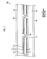
- Fig. 1 is a side view of the solar cell module 100 according to the first embodiment of the present invention.
- the solar cell module 100 includes a plurality of solar cells 10, a wiring member 20, a light-receiving-surface-side protective member 30, a back-surface-side protective member 40, and a sealing member 50.
- the solar cell 10 includes a solar cell substrate 11 and a protective layer 15 (not shown in Fig. 1 ; see Fig. 2 ).
- the solar cell substrate 11 includes a photoelectric conversion part 12, a thin wire electrode 13, and a connecting electrode 14.
- the solar cell 10 also has a light receiving surface (upper surface in the drawing) through which sunlight enters, and a back surface (bottom surface in the drawing) provided on the rear side of the light receiving surface.
- the light receiving surface and the back surface constitute main surfaces of the solar cell 10.
- the thin wire electrode 13 and the connecting electrode 14 are respectively formed on the light receiving surface of the solar cell 10 and on the back surface of the solar cell 10. A configuration of the solar cell 10 will be described later.
- the wiring member 20 electrically connects a plurality of solar cells 10 arranged in an arrangement direction.
- the wiring member 20 is connected to a connecting electrode 14 formed in the arrangement direction on the light receiving surface of one solar cell 10, and also connected to a connecting electrode 14 formed in the arrangement direction on the back surface of a different solar cell 10 adjacent to one side of the one solar cell 10.
- the wiring member 20 is connected to a connecting electrode 14 formed in the arrangement direction on the back surface of the one solar cell 10, and also connected to a connecting electrode 14 formed in the arrangement direction on the light receiving surface of still different solar cell 10 adjacent to the other side of the one solar cell 10.
- a conductive material such as copper molded into a thin plate shape or twisted line shape, can be used for the wiring member 20. It should be noted that soft conductive materials, such as eutectic solder, may be plated on a surface of the thin plate shape copper and the like used for the wiring member 20.
- the light-receiving-surface-side protective member 30 is disposed on the light receiving surface side of the sealing member 50 to protect the surface of the solar cell module 100.
- material having translucency and waterproofness such as glass, or translucent plastics, can be used.
- the back-surface-side protective member 40 is disposed on the back surface side of the sealing member 50 to protect the back surface of the solar cell module 100.
- a resin film such as polyethylene terephthalate (PET), a stacked film having a structure in which an Al foil is sandwiched between resin films and the like can be used.
- the sealing member 50 seals a plurality of solar cells 10 between the light-receiving-surface-side protective member 30 and the back-surface-side protective member 40, the plurality of solar cells 10 being electrically connected by the wiring member 20.
- resins having translucency such as EVA, EEA, PVB, silicone resins, urethane resins, acrylic resins, epoxy resins, can be used.
- An Al frame (not shown) can be attached to the circumference of the solar cell module 100 having the above-mentioned configuration.
- Fig. 2 is a plan view of the light receiving surface side of the solar cell 10 according to the first embodiment of the present invention.
- the solar cell 10 includes the solar cell substrate 11 and the protective layer 15.
- the solar cell substrate 11 includes the photoelectric conversion part 12, the thin wire electrode 13, and the connecting electrode 14.
- the photoelectric conversion part 12 generates a photocarrier by receiving the sunlight on the light receiving surface.
- the photocarrier refers to an electron hole and an electron which are generated from the sunlight being absorbed by the photoelectric conversion part 12.
- the photoelectric conversion part 12 has an n type region and a p type region therein. A semiconductor junction is formed at an interface portion of the n type region and the p type region in the photoelectric conversion part 12.
- the photoelectric conversion part 12 can be formed using a semiconductor substrate formed of semiconductor materials including crystalline semiconductor materials such as monocrystalline Si and polycrystalline Si, compound semiconductor materials such as GaAs, InP, etc.
- the photoelectric conversion part 12 may have the so-called HIT structure, i.e., a structure in which a substantially intrinsic amorphous silicon layer is sandwiched between a monocrystalline silicon substrate and an amorphous silicon layer, thereby reducing defects in the interface, and improving properties of a hetero junction interface.
- HIT structure i.e., a structure in which a substantially intrinsic amorphous silicon layer is sandwiched between a monocrystalline silicon substrate and an amorphous silicon layer, thereby reducing defects in the interface, and improving properties of a hetero junction interface.
- the thin wire electrode 13 is an electrode that collects the photogenerated carriers from the photoelectric conversion part 12. As shown in Fig. 2 , the thin wire electrode 13 is formed in a line form in a direction approximately perpendicular to the arrangement direction. A plurality of thin wire electrodes 13 are formed, for example, over the approximately whole region of the light receiving surface of the photoelectric conversion part 12.
- the thin wire electrode 13 can be formed using a resin-type conductive paste including a resin material as a binder and conductive particles such as silver particles as a filler, but the thin wire electrode 13 is not limited to be formed in this way. As shown in Fig. 1 , the thin wire electrode 13 is also formed on the back surface of the photoelectric conversion part 12.
- the connecting electrode 14 is an electrode that collects the photogenerated carriers from several thin wire electrodes 13. As shown in Fig. 2 , the connecting electrode 14 is formed in the arrangement direction in such a way to intersect with the thin wire electrode 13.
- the connecting electrode 14 can be formed using, for example, a resin-type conductive paste including a resin material as a binder and conductive particles such as silver particles as a filler, but the connecting electrode is not limited to be formed in this way. As shown in Fig. 1 , the connecting electrode 14 is also formed on the back surface of the photoelectric conversion part 12.
- the number of the connecting electrodes 14 can be set to a suitable number in consideration of size of the photoelectric conversion part 12 and the like.
- the solar cell 10 according to the first embodiment of the present invention includes a single connecting electrode 14.
- the protective layer 15 is a thin film that protects the light receiving surface of the solar cell substrate 11. Specifically, the protective layer 15 suppresses damages to a region on the light receiving surface of the solar cell substrate 11 where the photoelectric conversion part 12 is exposed, and damages to the thin wire electrode 13 formed on the light receiving surface of the photoelectric conversion part 12. In addition, the protective layer 15 blocks out, from the atmosphere, the region in which the light receiving surface of the photoelectric conversion part 12 is exposed. This prevents the components of the photoelectric conversion part 12 from being ionized due to moisture in the atmosphere, and the pn semiconductor junction of the photoelectric conversion part 12 from being deteriorated. Thus, the protective layer 15 protects the light receiving surface of the solar cell substrate 11 against damages and moisture, thereby, preventing reduction in photoelectric conversion efficiency of the solar cell substrate 11.
- translucent resins such as EVA, PVA, PVB, silicone resins, acrylic resins, epoxy resins, and polysilazane
- additives such as silicon oxide, aluminum oxide, magnesium oxide, titanium oxide, and zinc oxide, may be added to these resins.
- Fig. 3 is a sectional view taken along the line A-A of Fig. 2 .
- Fig. 4 is s sectional view taken along the line B-B of Fig. 2 .
- a region in which the light receiving surface of the solar cell substrate 11 is exposed is provided so as to surround the protective layer 15.
- the protective layer 15 is not formed and the light receiving surface is exposed in a region from the circumference of the light receiving surface of the solar cell substrate 11 to the inside by a predetermined distance.
- the protective layer 15 is not formed and the light receiving surface is exposed on the connecting electrode 14 and in the circumference of the connecting electrode 14.
- the protective layer 15 is formed on the thin wire electrode 13 and in the circumference of the thin wire electrode 13.
- the protective layer 15 is formed almost entirely over the light receiving surface of the solar cell substrate 11, the region in which the light receiving surface of the solar cell substrate 11 is exposed is provided so as to surround the protective layer 15.
- the protective layer 15 may be formed to be in contact with the side surfaces of the connecting electrode 14.
- a length in an arrangement direction of the protective layer 15 is approximately equal to that of the connecting electrode 14 in Fig. 2 .
- the length in the arrangement direction of the protective layer 15 may be different from that of the connecting electrode 14.
- the protective layer 15 When the length in the arrangement direction of the protective layer 15 is set to be longer than that of the connecting electrode 14, the protective layer 15 may be formed so as to surround the connecting electrode 14, as shown in Fig. 5 . In this case, in order to prevent a space from being left between the connecting electrode 14 and the wiring member 20 bonded thereon, the protective layer 15 preferably has a thickness smaller than that of the connecting electrode 14, the protective layer 15 being formed in an extension of the connecting electrode 14 on the light receiving surface of the solar cell substrate 11.
- the photoelectric conversion part 12 is formed.
- a plurality of thin wire electrodes 13 are formed in a first direction on the light receiving surface of the photoelectric conversion part 12.
- a connecting electrode 14 is formed on the light receiving surface of the photoelectric conversion part 12 in a second direction approximately perpendicular to the first direction.
- a plurality of thin wire electrodes 13 and another connecting electrode 14 are also formed on the back surface of the photoelectric conversion part 12. In this way, the solar cell substrate 11 is formed.
- the protective layer 15 formed of a translucent resin is formed on the light receiving surface of the solar cell substrate 11.
- a region in which the light receiving surface of the solar cell substrate 11 is exposed is provided so as to surround the protective layer 15.
- methods for example, offset printing method, roll coating method, etc.
- a liquid or gel translucent resin applied to a curved surface of a roller is transferred on the light receiving surface of the photoelectric conversion part 12 with the roller being rolled.
- Fig. 6 is a schematic diagram showing a method for forming the protective layer according to the first embodiment of the present invention.
- Concave portions having a specific pattern are formed on a curved surface of a cylindrical printing cylinder 61.
- the specific pattern refers to a shape corresponding to a shape of the protective layer 15 to be formed on the light receiving surface of the solar cell substrate 11.
- the specific pattern can be the shape of the protective layer 15 shown in Fig. 2 .
- the liquid or gel resin is accumulated in a resin tub 62.
- the rotating printing cylinder 61 is dipped in the liquid or gel resin accumulated in the resin tub 62. Accordingly, on the curved surface of the printing cylinder 61, the resin attached to a region other than the concave portions is removed, so the resin remains only in the concave portions. On the curved surface of the printing cylinder 61, it is not needed to have difference in height between the region in which the resin is removed and the region in which the resin remains. Specifically, the region in which the resin is removed may be chemically separated from the region in which the resin remains.
- a curved surface of a cylindrical blanket 63 is formed of an elastic member.
- the blanket 63 rotates in a direction opposite to a rotating direction of the printing cylinder 61, while causing its curved surface being in contact with the curved surface of the printing cylinder 61.
- the resin remaining in the concave portions of the printing cylinder 61 is transferred on the curved surface of the blanket 63.
- the resin to be transferred onto the curved surface of the blanket 63 has the specific pattern.
- the resin having the specific pattern is referred to as a specific pattern resin 64.
- a conveying device 65 conveys the solar cell substrate 11 mounted on a flat mounting base 66 in a predetermined conveying direction.
- the solar cell substrate 11 is mounted on the mounting base 66 with the light receiving surface facing upward.
- a belt conveyor, etc. can be used as the conveying device 65.
- the conveying device 65 causes the solar cell substrate 11 mounted on the mounting base 66 to pass through under the rotating blanket 63.
- the specific pattern resin 64 transferred onto the curved surface of the blanket 63 is transferred on the light receiving surface of the solar cell substrate 11.
- the liquid or gel specific pattern resin 64 transferred onto the light receiving surface of the solar cell substrate 11 is cured by drying. Thereby, the protective layer 15 is formed on the light receiving surface of the solar cell substrate 11, and consequently, the solar cell 10 is made.
- the wiring member 20 is connected to the connecting electrode 14 formed on the light receiving surface of the photoelectric conversion part 12, the wiring member 20 connecting one solar cell 10 including the photoelectric conversion part 12 with different solar cell 10 adjacent to one side of the one solar cell 10. Additionally, the wiring member 20 is connected to the connecting electrode 14 formed on the back surface of the photoelectric conversion part 12, the wiring member 20 connecting the one solar cell 10 including the photoelectric conversion part 12 with still different solar cell 10 adjacent to the other side of the one solar cell 10. Thereby, the one solar cell 10, the different solar cell 10 adjacent to the one side of the one solar cell 10, and the still different solar cell 10 adjacent to the other side of the one solar cell 10 are electrically connected.
- the sealing member 50 On the light-receiving-surface-side protective member 30, the sealing member 50, a plurality of solar cells 10 each being connected to each other by the wiring member 20, and the sealing member 50 and the back-surface-side protective member 40 are sequentially stacked so as to form a stacked body.
- the solar cell module 100 is manufactured by thermal compressing the stacked body in a vacuum atmosphere.
- the region in which the light receiving surface of the solar cell substrate 11 is exposed is formed on the outside of the circumference of the protective layer 15 formed on the light receiving surface of the solar cell substrate 11.
- the translucent resin that forms the protective layer 15 has high fluidity immediately after being transferred onto the light receiving surface of the solar cell substrate 11, the translucent resin can avoid overflowing to the outside of the light receiving surface of the solar cell substrate 11.
- the translucent resin that forms the protective layer 15 is prevented from intruding into a space between the solar cell substrate 11 and the mounting base 66, thus, is prevented from adhering onto the connecting electrode 14 formed on the back surface of the solar cell substrate 11. Consequently, faulty connection between the connecting electrode 14 formed on the back surface of the solar cell substrate 11 and the wiring member 20 can be prevented from occurring.
- the solar cell substrate 11 and the mounting base 66 it is possible to prevent the solar cell substrate 11 and the mounting base 66 from being fixed to each other. Therefore, the solar cell substrate 11 having the protective layer 15 formed on the light receiving surface can be prevented from being damaged when being detached from the mounting base 66. Consequently, it is possible to avoid reduction in the production efficiency of the solar cell substrate 11 having the protective layer 15 formed on the light receiving surface, i.e., the solar cell 10.
- a solar cell according to Example 1 was manufactured in the following way.
- a solar cell substrate including, on the light receiving, a plurality of thin wire electrodes formed in the first direction and the connecting electrode formed in the second direction approximately perpendicular to the first direction surface.
- an acrylic resin having the specific pattern was transferred on the light receiving surface of the solar cell substrate formed into 100 mm square.
- the area of the specific pattern was formed smaller than the area of the light receiving surface of the solar cell substrate. Accordingly, the region in which the light receiving surface of the solar cell substrate is exposed was provided so as to surround the acrylic resin transferred onto the light receiving surface of the solar cell substrate.
- Fig. 7 is a plan view of the light receiving surface side of the solar cell according to the example.
- a width ⁇ of the region in which the light receiving surface of the solar cell substrate is exposed was set to be 1 mm. Even when the width ⁇ of the region in which the light receiving surface of the solar cell substrate is exposed was 1 mm, the acrylic resin did not overflow to the outside of the circumference of the light receiving surface of the solar cell substrate.
- a solar cell according to Example 2 was manufactured in the following way.
- the width ⁇ of the region in which the light receiving surface of the solar cell substrate is exposed was set to be 2 mm. Even when the width ⁇ of the region in which the light receiving surface of the solar cell substrate is exposed was 2 mm, the acrylic resin did not overflow to the outside of the circumference of the light receiving surface of the solar cell substrate.
- a solar cell according to Comparative Example 1 was manufactured in the following way.
- Comparative Example 2 a solar cell substrate similar to those in Example 1 and Example 2 mentioned above was prepared. However, in Comparative Example 2, the entire light receiving surface was exposed without forming a protective layer on the light receiving surface of the solar cell substrate.
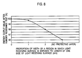
- Fig. 8 is diagram showing each energy output value of the solar cells according to Example 1, Example 2, Comparative Example 1, and Comparative Example 2 after the humidity resistance test.
- the test conditions were set at a temperature of 85°C and at a humidity of 85%, and a test period was set at 1000 hours.
- the energy output values of the solar cells according to Example 1, Example 2, and Comparative Example 2 after the humidity resistance test are shown as the normalized value by using the energy output value of the solar cell according to Comparative Example 1 after the humidity resistance test being defined as 1.00.
- the solar cell according to Example 1 was able to maintain 99.7% of the energy output value of the solar cell according to Comparative Example 1 after the humidity resistance test.
- the solar cell according to Example 2 was able to maintain 98.0% of the energy output value of the solar cell according to Comparative Example 1 after the humidity resistance test.
- the solar cell according to Comparative Example 2 was able to maintain only 96.0% of the energy output value of the solar cell according to Comparative Example 1 after the humidity resistance test.
- the reason is that the protective layer is not formed on the light receiving surface of the solar cell substrate in Comparative Example 2. Therefore, moisture in the atmosphere permeates through the photoelectric conversion part more easily, compared with Example 1, Example 2, and Comparative Example 1 so that of the pn semiconductor junction of the photoelectric conversion part is deteriorated in higher extent.
- loss of the energy output value can be limited within 2% of the energy output value of the solar cell having the protective layer entirely formed over the light receiving surface after the humidity resistance test.
- the width ⁇ of the region in which the light receiving surface is exposed is particularly preferably not more than 1 mm.
- the protective layer is formed only on the light receiving surface of the solar cell, and in the second embodiment, the protective layer is formed on the light receiving surface as well as the back surface of the solar cell 10, but the present invention is not limited to these.
- the protective layer may be formed only on the back surface of the solar cell.
- the protective layer may be formed on both of the light receiving surface and the back surface.
- the protective layer is formed on a surface close to a region in which the pn semiconductor junction is formed within the photoelectric conversion part. The reason is that the photoelectric conversion efficiency of the solar cell is easily reduced when the pn semiconductor junction is deteriorated due to moisture that permeates through the photoelectric conversion part.
- the protective layer is formed by the offset printing method or roll coating method, but the present invention is not limited to these. Specifically, the protective layer may be formed using alternative coating methods, such as spray method, screen printing method, and dip method.
- the photoelectric conversion part includes the connecting electrode, but the present invention is not limited to this. Specifically, the photoelectric conversion part may not include the connecting electrode, and the wiring member may be directly connected to the thin wire electrode.
- the thin wire electrode and the connecting electrode are formed in a comb shape on the back surface of the photoelectric conversion part, but the present invention is not limited to this.
- a collector electrode that collects the photogenerated carriers may be formed to cover the whole back surface of the photoelectric conversion part.
- the present invention does not limit the shape of the collector electrode formed on the back surface of the photoelectric conversion part.
- the thin wire electrode is formed in a line form in the direction approximately perpendicular to the arrangement direction of the plurality solar cells, but the thin wire electrode does not need to be in a line form.
- the present invention does not limit the shape of the thin wire electrode.
- the width of the region in which the light receiving surface is exposed may be increased or decreased depending on a kind of a translucent resin that forms the protective layer, viscosity of the translucent resin when transferring the translucent resin on the light receiving surface or back surface of the solar cell, or the like.
Landscapes
- Photovoltaic Devices (AREA)
Applications Claiming Priority (1)
| Application Number | Priority Date | Filing Date | Title |
|---|---|---|---|
| JP2007219294A JP5147332B2 (ja) | 2007-08-27 | 2007-08-27 | 太陽電池モジュール、太陽電池、及びこれらの製造方法 |
Publications (2)
| Publication Number | Publication Date |
|---|---|
| EP2031663A2 true EP2031663A2 (fr) | 2009-03-04 |
| EP2031663A3 EP2031663A3 (fr) | 2011-05-04 |
Family
ID=40123963
Family Applications (1)
| Application Number | Title | Priority Date | Filing Date |
|---|---|---|---|
| EP08252822A Withdrawn EP2031663A3 (fr) | 2007-08-27 | 2008-08-26 | Module de cellule solaire, son procédé de fabrication, cellule solaire et son procédé de fabrication |
Country Status (3)
| Country | Link |
|---|---|
| US (1) | US20090056803A1 (fr) |
| EP (1) | EP2031663A3 (fr) |
| JP (1) | JP5147332B2 (fr) |
Cited By (2)
| Publication number | Priority date | Publication date | Assignee | Title |
|---|---|---|---|---|
| WO2012127397A1 (fr) * | 2011-03-18 | 2012-09-27 | Somont Gmbh | Procédés et système pour fabriquer au moins un dispositif photovoltaïque avec au moins un élément protecteur |
| CN107757044A (zh) * | 2017-09-20 | 2018-03-06 | 东营大海科林光电有限公司 | 一种太阳能电池组件敷设层压方法 |
Families Citing this family (21)
| Publication number | Priority date | Publication date | Assignee | Title |
|---|---|---|---|---|
| US9012766B2 (en) | 2009-11-12 | 2015-04-21 | Silevo, Inc. | Aluminum grid as backside conductor on epitaxial silicon thin film solar cells |
| TW201125140A (en) * | 2010-01-14 | 2011-07-16 | Motech Ind Inc | Solar cell module |
| US9214576B2 (en) | 2010-06-09 | 2015-12-15 | Solarcity Corporation | Transparent conducting oxide for photovoltaic devices |
| US9773928B2 (en) | 2010-09-10 | 2017-09-26 | Tesla, Inc. | Solar cell with electroplated metal grid |
| US9800053B2 (en) | 2010-10-08 | 2017-10-24 | Tesla, Inc. | Solar panels with integrated cell-level MPPT devices |
| US8134067B1 (en) * | 2011-01-21 | 2012-03-13 | Chin-Yao Tsai | Thin film photovoltaic device |
| US9054256B2 (en) | 2011-06-02 | 2015-06-09 | Solarcity Corporation | Tunneling-junction solar cell with copper grid for concentrated photovoltaic application |
| EP2752889B1 (fr) * | 2011-08-31 | 2018-11-28 | Panasonic Intellectual Property Management Co., Ltd. | Procédé de fabrication de module de piles solaires |
| US9865754B2 (en) | 2012-10-10 | 2018-01-09 | Tesla, Inc. | Hole collectors for silicon photovoltaic cells |
| US10074755B2 (en) | 2013-01-11 | 2018-09-11 | Tesla, Inc. | High efficiency solar panel |
| US9219174B2 (en) | 2013-01-11 | 2015-12-22 | Solarcity Corporation | Module fabrication of solar cells with low resistivity electrodes |
| US9412884B2 (en) * | 2013-01-11 | 2016-08-09 | Solarcity Corporation | Module fabrication of solar cells with low resistivity electrodes |
| JP5695283B1 (ja) * | 2013-05-17 | 2015-04-01 | 株式会社カネカ | 太陽電池およびその製造方法、ならびに太陽電池モジュール |
| US10309012B2 (en) | 2014-07-03 | 2019-06-04 | Tesla, Inc. | Wafer carrier for reducing contamination from carbon particles and outgassing |
| US9899546B2 (en) | 2014-12-05 | 2018-02-20 | Tesla, Inc. | Photovoltaic cells with electrodes adapted to house conductive paste |
| US9761744B2 (en) | 2015-10-22 | 2017-09-12 | Tesla, Inc. | System and method for manufacturing photovoltaic structures with a metal seed layer |
| US9842956B2 (en) | 2015-12-21 | 2017-12-12 | Tesla, Inc. | System and method for mass-production of high-efficiency photovoltaic structures |
| US10115838B2 (en) | 2016-04-19 | 2018-10-30 | Tesla, Inc. | Photovoltaic structures with interlocking busbars |
| US10672919B2 (en) | 2017-09-19 | 2020-06-02 | Tesla, Inc. | Moisture-resistant solar cells for solar roof tiles |
| US11190128B2 (en) | 2018-02-27 | 2021-11-30 | Tesla, Inc. | Parallel-connected solar roof tile modules |
| US11581843B2 (en) * | 2018-09-14 | 2023-02-14 | Tesla, Inc. | Solar roof tile free of back encapsulant layer |
Citations (1)
| Publication number | Priority date | Publication date | Assignee | Title |
|---|---|---|---|---|
| JP2007141967A (ja) | 2005-11-15 | 2007-06-07 | Sanyo Electric Co Ltd | 光起電力素子、光起電力モジュールおよび光起電力素子の製造方法 |
Family Cites Families (18)
| Publication number | Priority date | Publication date | Assignee | Title |
|---|---|---|---|---|
| JPS5950572A (ja) * | 1982-09-16 | 1984-03-23 | Hitachi Ltd | 非晶質シリコン太陽電池 |
| JPH0712078B2 (ja) * | 1985-10-23 | 1995-02-08 | 株式会社日立製作所 | 受光素子の製造方法 |
| JPS6459875A (en) * | 1987-08-31 | 1989-03-07 | Matsushita Electric Industrial Co Ltd | Solar battery module |
| JPH065773B2 (ja) * | 1987-11-16 | 1994-01-19 | 株式会社富士電機総合研究所 | 薄膜太陽電池 |
| JP2938634B2 (ja) * | 1991-10-08 | 1999-08-23 | キヤノン株式会社 | 太陽電池モジュール |
| US5457057A (en) * | 1994-06-28 | 1995-10-10 | United Solar Systems Corporation | Photovoltaic module fabrication process |
| JP3352252B2 (ja) * | 1994-11-04 | 2002-12-03 | キヤノン株式会社 | 太陽電池素子群並びに太陽電池モジュール及びその製造方法 |
| DE69736151T2 (de) * | 1996-05-17 | 2007-05-10 | Canon K.K. | Photovoltaische Anordnung und Herstellungsverfahren |
| JP3516156B2 (ja) * | 1997-12-16 | 2004-04-05 | シャープ株式会社 | 太陽電池の製造方法および保護カバー用素材板 |
| US6175075B1 (en) * | 1998-04-21 | 2001-01-16 | Canon Kabushiki Kaisha | Solar cell module excelling in reliability |
| US6262358B1 (en) * | 1999-02-18 | 2001-07-17 | Sharp Kabushiki Kaisha | Solar cell module and solar cell panel using the same |
| US6166322A (en) * | 1999-04-16 | 2000-12-26 | Industrial Technology Research Institute | Encapulation process for mono-and polycrystalline silicon solar cell modules |
| JP2002217431A (ja) * | 2001-01-16 | 2002-08-02 | Canon Inc | 耐候性光起電力素子およびその製造方法、設置方法、並びにその耐候性光起電力素子を用いた発電システム |
| JP2002373998A (ja) * | 2001-06-15 | 2002-12-26 | Fuji Electric Co Ltd | 太陽電池モジュールとその製造方法 |
| JP3905756B2 (ja) * | 2001-12-28 | 2007-04-18 | シャープ株式会社 | 補強半導体基板の製造方法及び製造装置 |
| JP3910075B2 (ja) * | 2002-02-08 | 2007-04-25 | シャープ株式会社 | 太陽電池用基板上に補強膜を形成する方法 |
| JPWO2005109524A1 (ja) * | 2004-05-07 | 2008-03-21 | 三菱電機株式会社 | 太陽電池及びその製造方法 |
| JP5121181B2 (ja) * | 2006-07-28 | 2013-01-16 | 三洋電機株式会社 | 光起電力素子及びその製造方法 |
-
2007
- 2007-08-27 JP JP2007219294A patent/JP5147332B2/ja not_active Expired - Fee Related
-
2008
- 2008-08-26 US US12/198,214 patent/US20090056803A1/en not_active Abandoned
- 2008-08-26 EP EP08252822A patent/EP2031663A3/fr not_active Withdrawn
Patent Citations (1)
| Publication number | Priority date | Publication date | Assignee | Title |
|---|---|---|---|---|
| JP2007141967A (ja) | 2005-11-15 | 2007-06-07 | Sanyo Electric Co Ltd | 光起電力素子、光起電力モジュールおよび光起電力素子の製造方法 |
Cited By (2)
| Publication number | Priority date | Publication date | Assignee | Title |
|---|---|---|---|---|
| WO2012127397A1 (fr) * | 2011-03-18 | 2012-09-27 | Somont Gmbh | Procédés et système pour fabriquer au moins un dispositif photovoltaïque avec au moins un élément protecteur |
| CN107757044A (zh) * | 2017-09-20 | 2018-03-06 | 东营大海科林光电有限公司 | 一种太阳能电池组件敷设层压方法 |
Also Published As
| Publication number | Publication date |
|---|---|
| JP5147332B2 (ja) | 2013-02-20 |
| US20090056803A1 (en) | 2009-03-05 |
| JP2009054748A (ja) | 2009-03-12 |
| EP2031663A3 (fr) | 2011-05-04 |
Similar Documents
| Publication | Publication Date | Title |
|---|---|---|
| EP2031663A2 (fr) | Module de cellule solaire, son procédé de fabrication, cellule solaire et son procédé de fabrication | |
| US10319869B2 (en) | Solar battery, method for manufacturing solar battery, method for manufacturing solar cell module, and solar cell module | |
| EP2020688B1 (fr) | Connection entre cellules solaires dans un module utilisant le bonding par thermo-compression et un tel module | |
| EP2549549B1 (fr) | Module de cellule solaire | |
| US20130112234A1 (en) | Solar cell module | |
| KR101514844B1 (ko) | 태양 전지 모듈 및 그 제조 방법 | |
| US20080196757A1 (en) | Solar cell and solar cell module | |
| KR101465924B1 (ko) | 태양 전지 모듈의 제조 방법 및 태양 전지 모듈 | |
| US9608140B2 (en) | Solar cell and solar cell module | |
| US20120125391A1 (en) | Methods for interconnecting photovoltaic cells | |
| US20100243027A1 (en) | Solar cell and solar cell module | |
| US20090301555A1 (en) | Solar cell, solar module and system and fabrication method thereof | |
| EP2249397A1 (fr) | Module de pile solaire | |
| EP2375454B1 (fr) | Module de piles solaires et son procédé de fabrication | |
| US7803651B2 (en) | Method of manufacturing solar cell module and method of manufacturing solar cell | |
| EP2237324A1 (fr) | Panneau solaire et son procédé de fabrication | |
| US20120073621A1 (en) | Solar cell and solar cell module | |
| EP2461371A2 (fr) | Module de cellule solaire | |
| US20160043249A1 (en) | Solar cell module and method of fabricating the same | |
| EP2040311A2 (fr) | Procédé de fabrication de cellule solaire | |
| JP2007141967A (ja) | 光起電力素子、光起電力モジュールおよび光起電力素子の製造方法 | |
| KR101120100B1 (ko) | 박막태양전지모듈 및 그 제조방법과 모듈 상호간의 연결방법 | |
| CN223274440U (zh) | 层压组件和光伏组件 | |
| KR101305682B1 (ko) | 태양광 발전 장치 및 이의 제조 방법 | |
| US9853170B2 (en) | Solar cell module manufacturing method |
Legal Events
| Date | Code | Title | Description |
|---|---|---|---|
| PUAI | Public reference made under article 153(3) epc to a published international application that has entered the european phase |
Free format text: ORIGINAL CODE: 0009012 |
|
| AK | Designated contracting states |
Kind code of ref document: A2 Designated state(s): AT BE BG CH CY CZ DE DK EE ES FI FR GB GR HR HU IE IS IT LI LT LU LV MC MT NL NO PL PT RO SE SI SK TR |
|
| AX | Request for extension of the european patent |
Extension state: AL BA MK RS |
|
| PUAL | Search report despatched |
Free format text: ORIGINAL CODE: 0009013 |
|
| AK | Designated contracting states |
Kind code of ref document: A3 Designated state(s): AT BE BG CH CY CZ DE DK EE ES FI FR GB GR HR HU IE IS IT LI LT LU LV MC MT NL NO PL PT RO SE SI SK TR |
|
| AX | Request for extension of the european patent |
Extension state: AL BA MK RS |
|
| 17P | Request for examination filed |
Effective date: 20111103 |
|
| AKX | Designation fees paid |
Designated state(s): AT BE BG CH CY CZ DE DK EE ES FI FR GB GR HR HU IE IS IT LI LT LU LV MC MT NL NO PL PT RO SE SI SK TR |
|
| STAA | Information on the status of an ep patent application or granted ep patent |
Free format text: STATUS: THE APPLICATION HAS BEEN WITHDRAWN |
|
| 18W | Application withdrawn |
Effective date: 20140715 |