EP2023442A2 - Mehrteilige Platine - Google Patents
Mehrteilige Platine Download PDFInfo
- Publication number
- EP2023442A2 EP2023442A2 EP08013738A EP08013738A EP2023442A2 EP 2023442 A2 EP2023442 A2 EP 2023442A2 EP 08013738 A EP08013738 A EP 08013738A EP 08013738 A EP08013738 A EP 08013738A EP 2023442 A2 EP2023442 A2 EP 2023442A2
- Authority
- EP
- European Patent Office
- Prior art keywords
- sub
- clamping
- board
- boards
- circuit board
- Prior art date
- Legal status (The legal status is an assumption and is not a legal conclusion. Google has not performed a legal analysis and makes no representation as to the accuracy of the status listed.)
- Withdrawn
Links
Images
Classifications
-
- H—ELECTRICITY
- H01—ELECTRIC ELEMENTS
- H01R—ELECTRICALLY-CONDUCTIVE CONNECTIONS; STRUCTURAL ASSOCIATIONS OF A PLURALITY OF MUTUALLY-INSULATED ELECTRICAL CONNECTING ELEMENTS; COUPLING DEVICES; CURRENT COLLECTORS
- H01R12/00—Structural associations of a plurality of mutually-insulated electrical connecting elements, specially adapted for printed circuits, e.g. printed circuit boards [PCB], flat or ribbon cables, or like generally planar structures, e.g. terminal strips, terminal blocks; Coupling devices specially adapted for printed circuits, flat or ribbon cables, or like generally planar structures; Terminals specially adapted for contact with, or insertion into, printed circuits, flat or ribbon cables, or like generally planar structures
- H01R12/50—Fixed connections
- H01R12/51—Fixed connections for rigid printed circuits or like structures
- H01R12/52—Fixed connections for rigid printed circuits or like structures connecting to other rigid printed circuits or like structures
-
- H—ELECTRICITY
- H05—ELECTRIC TECHNIQUES NOT OTHERWISE PROVIDED FOR
- H05K—PRINTED CIRCUITS; CASINGS OR CONSTRUCTIONAL DETAILS OF ELECTRIC APPARATUS; MANUFACTURE OF ASSEMBLAGES OF ELECTRICAL COMPONENTS
- H05K1/00—Printed circuits
- H05K1/02—Details
- H05K1/14—Structural association of two or more printed circuits
-
- H—ELECTRICITY
- H05—ELECTRIC TECHNIQUES NOT OTHERWISE PROVIDED FOR
- H05K—PRINTED CIRCUITS; CASINGS OR CONSTRUCTIONAL DETAILS OF ELECTRIC APPARATUS; MANUFACTURE OF ASSEMBLAGES OF ELECTRICAL COMPONENTS
- H05K1/00—Printed circuits
- H05K1/02—Details
- H05K1/14—Structural association of two or more printed circuits
- H05K1/148—Arrangements of two or more hingeably connected rigid printed circuit boards, i.e. connected by flexible means
-
- H—ELECTRICITY
- H05—ELECTRIC TECHNIQUES NOT OTHERWISE PROVIDED FOR
- H05K—PRINTED CIRCUITS; CASINGS OR CONSTRUCTIONAL DETAILS OF ELECTRIC APPARATUS; MANUFACTURE OF ASSEMBLAGES OF ELECTRICAL COMPONENTS
- H05K2201/00—Indexing scheme relating to printed circuits covered by H05K1/00
- H05K2201/04—Assemblies of printed circuits
- H05K2201/047—Box-like arrangements of PCBs
-
- H—ELECTRICITY
- H05—ELECTRIC TECHNIQUES NOT OTHERWISE PROVIDED FOR
- H05K—PRINTED CIRCUITS; CASINGS OR CONSTRUCTIONAL DETAILS OF ELECTRIC APPARATUS; MANUFACTURE OF ASSEMBLAGES OF ELECTRICAL COMPONENTS
- H05K2201/00—Indexing scheme relating to printed circuits covered by H05K1/00
- H05K2201/04—Assemblies of printed circuits
- H05K2201/048—Second PCB mounted on first PCB by inserting in window or holes of the first PCB
-
- H—ELECTRICITY
- H05—ELECTRIC TECHNIQUES NOT OTHERWISE PROVIDED FOR
- H05K—PRINTED CIRCUITS; CASINGS OR CONSTRUCTIONAL DETAILS OF ELECTRIC APPARATUS; MANUFACTURE OF ASSEMBLAGES OF ELECTRICAL COMPONENTS
- H05K2201/00—Indexing scheme relating to printed circuits covered by H05K1/00
- H05K2201/10—Details of components or other objects attached to or integrated in a printed circuit board
- H05K2201/10431—Details of mounted components
- H05K2201/1059—Connections made by press-fit insertion
-
- H—ELECTRICITY
- H05—ELECTRIC TECHNIQUES NOT OTHERWISE PROVIDED FOR
- H05K—PRINTED CIRCUITS; CASINGS OR CONSTRUCTIONAL DETAILS OF ELECTRIC APPARATUS; MANUFACTURE OF ASSEMBLAGES OF ELECTRICAL COMPONENTS
- H05K2201/00—Indexing scheme relating to printed circuits covered by H05K1/00
- H05K2201/10—Details of components or other objects attached to or integrated in a printed circuit board
- H05K2201/10431—Details of mounted components
- H05K2201/10598—Means for fastening a component, a casing or a heat sink whereby a pressure is exerted on the component towards the PCB
-
- H—ELECTRICITY
- H05—ELECTRIC TECHNIQUES NOT OTHERWISE PROVIDED FOR
- H05K—PRINTED CIRCUITS; CASINGS OR CONSTRUCTIONAL DETAILS OF ELECTRIC APPARATUS; MANUFACTURE OF ASSEMBLAGES OF ELECTRICAL COMPONENTS
- H05K3/00—Apparatus or processes for manufacturing printed circuits
- H05K3/36—Assembling printed circuits with other printed circuits
- H05K3/366—Assembling printed circuits with other printed circuits substantially perpendicularly to each other
Definitions
- the invention relates to a multi-part board, according to the o-berbefifflichen features of a patent claim 1.
- Multi-part circuit boards are known from the prior art to accommodate larger circuit arrangements, in, for example, cylindrically shaped housings.
- Such a multi-part circuit board consists of several sub-boards, which are connected to each other via flexible signal connections, eg. Ribbon cable and is angled in an insert configuration between the sub-boards, so that, for example.
- a four-sided hollow cylinder is formed, which can be inserted into the cylindrically shaped housing .
- PCB spacers are known with which multi-part boards can be fixed at a certain distance from each other.
- a disadvantage of such connectivity options is that fixation by means of connectors or frames causes additional operations for mounting these accessories, as well as the corresponding costs for the accessories.
- fixation by means of connectors or frames causes additional operations for mounting these accessories, as well as the corresponding costs for the accessories.
- problems can also occur by chemical reactions of the adhesive with other potting compounds, or the boards. This is time-consuming and expensive and involves further sources of error and / or problems.
- a multi-part circuit board according to the invention has at least two sub-boards and interposed flexible connections, wherein on a first sub-board at least one clamping element is formed, which is insertable into at least one clamping opening of another sub-board.
- the multi-part board it is possible to fix two sub-boards to each other without further assembly elements or a bond are necessary.
- An advantage of such a configuration is in particular a short assembly time, as well as an increased temperature resistance of the clamping connection in comparison to e.g. Adhesive bonds.
- the clamping opening is formed as a clamping slot and the clamping element is integrally formed, preferably laterally to the sub-board and consists of board material.
- the clamping element is integrally formed, preferably laterally to the sub-board and consists of board material.
- a plurality, in particular two, clamping noses and clamping slots are provided.
- An advantage of such an embodiment is that a parallel arrangement of a plurality of clamping lugs along a platinum edge a rotationally secure fixation of the boards is ensured to each other.
- sub-boards which have mutually parallel side edges and the flexible connections are designed as connecting lines and / or signal lines.
- an embodiment of the invention is preferably used because the sub-boards are in their preferred positioning at 90 ° to each other and so a particularly effective fixation can be achieved by an arrangement with clamping lugs and clamping slots.
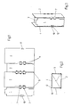
- FIG. 1 shows an embodiment of a multi-part board according to the invention, in its basic configuration.
- the multi-part board consists of four sub-boards 1, 2, 3, 4, which are rigidly interconnected in the basic configuration.
- the multi-part board is equipped with components and processed to their full functionality and then tested. After a successful test, the multi-part board is divided at separation points 8 in the sub-boards 1, 2, 3, 4 and can then be brought into application configuration.
- a clamping lug 10 is formed, which is insertable into a clamping slot 12 of a fourth board 4 of the multi-part board.
- the individual sub-boards 1, 2, 3, 4 preferably have parallel edges 9, so that the multi-part board, as in the FIGS.
- the clamping lug 10 is formed as a laterally slotted spring element with a first leg 10a and a second leg 10b. If the clamping lug 10 is inserted into the clamping slot 12, the first leg 10a and the second leg 10b of the clamping lug 10 move toward one another and jam in the clamping slot 12. To facilitate insertion of the clamping lug 10 in the clamping slot 12 to ensure the legs 10a, 10b chamfered at its front edge.
- FIG. 2 shows a plan view of the multi-part board FIG. 1 in application configuration.
- the multi-part circuit board has a cross section in the form of a square.
- each of the individual sub-boards 1, 2, 3, 4 are arranged.
- the clamping lug 10 of the first sub-board 1 is inserted into the clamping slot 12 of the fourth sub-board 4, so that the orientation of the first sub-board 1 to the fourth sub-board 4 is fixed by a 90 ° angle and the alignment of the second sub-board 2 and the third Sub-board 3 determined.
- the first sub-board 1 and the fourth sub-board 4 are connected via the clamping connection, wherein the further sub-boards 1, 2, 3, 4, are interconnected by the flexible signal connections 7.
- FIG. 3 shows a perspective view of the multi-part board in application configuration. Clearly visible in this illustration is the square basic shape of the multi-part board, as well as the clamping connection between the first sub-board 1 and the fourth sub-board 4 by the clamping lug 10, which is guided through the clamping slot 12.
Landscapes
- Engineering & Computer Science (AREA)
- Microelectronics & Electronic Packaging (AREA)
- Combinations Of Printed Boards (AREA)
Abstract
Description
- Die Erfindung betrifft eine mehrteilige Platine, gemäß den o-berbegrifflichen Merkmalen eines Patentanspruchs 1.
- Mehrteilige Platinen sind aus dem Stand der Technik bekannt, um größere Schaltungsanordnungen, in bspw. zylindrisch ausgeformten Gehäusen unterzubringen. Eine derartige mehrteilige Platine besteht dabei aus mehreren Teilplatinen, die über flexible Signalverbindungen, bspw. Bandkabel, miteinander verbunden sind und wird in einer Einsatzkonfiguration zwischen den Teilplatinen abgewinkelt, so dass bspw. ein vierseitiger Hohlzylinder entsteht, der in das zylindrisch ausgeformte Gehäuse eingeschoben werden kann. Um die einzelnen Teilplatinen in einer definierten Position zueinander zu fixieren, ist es nach dem Stand der Technik üblich, die einzelnen Teilplatinen zu verkleben oder durch weitere Zubehörteile, bspw. Steckverbindern oder Rahmen, relativ zueinander zu fixieren. Von der Firma Skiffy sind beispielsweise sogenannte PCB Spacer bekannt, mit denen mehrteilige Platinen in einem bestimmten Abstand zueinander fixiert werden können.
- Nachteilig an solchen Verbindungsmöglichkeiten ist, dass eine Fixierung mittels Steckverbindern oder Rahmen zusätzliche Arbeitsgänge zur Montage dieser Zubehörteile, sowie die entsprechenden Kosten für die Zubehörteile verursacht. Für den Fall, dass die Leiterplatten miteinander verklebt werden, können des Weiteren Probleme durch chemische Reaktionen des Klebstoffes mit anderen Vergussmassen, bzw. den Platinen auftreten. Dies ist zeit- und kostenintensiv und birgt weitere Fehler- und/oder Problemquellen.
- Es ist die Aufgabe der Erfindung eine mehrteilige Platine zur Verfügung zu stellen, mit der es möglich ist, zwei oder mehrere Leiterplatten ohne weitere Montageteile in einer definierten Position zueinander fixieren. Des Weiteren soll eine schnellere und günstigere Montage der mehrteiligen Platine möglich sein.
- Diese Aufgabe wird gelöst durch eine mehrteilige Platine mit den Merkmalen des Patentanspruchs 1.
- Eine erfindungsgemäße mehrteilige Platine weist wenigstens zwei Teilplatinen und dazwischen angeordnete, flexible Verbindungen auf, wobei an einer ersten Teilplatine wenigstens ein Klemmelement angeformt ist, das in wenigstens eine Klemmöffnung einer anderen Teilplatine einführbar ist.
- Durch eine erfindungsgemäße Ausgestaltung, der mehrteiligen Platine ist es möglich, zwei Teilplatinen zueinander zu fixieren ohne dass weitere Montageelemente oder eine Klebung notwendig sind. Vorteilhaft an der derartigen Ausgestaltung ist insbesondere eine geringe Montagezeit, sowie eine erhöhte Temperaturbeständigkeit der Klemmverbindung im Vergleich zu z.B. Klebeverbindungen.
- In einer bevorzugten Ausgestaltungsform der Erfindung ist die Klemmöffnung als Klemmschlitz ausgebildet und das Klemmelement ist einstückig, vorzugsweise seitlich an die Teilplatine angeformt und besteht aus Platinenmaterial. An dieser bevorzugten Ausgestaltungsvariante ist besonders vorteilhaft, dass eine Herstellung von Platine und Klemmelement in einem Arbeitsgang möglich ist und eine Fixierung auf einfache Art und Weise stattfinden kann.
- Gemäß einer weiter bevorzugten Ausgestaltungsform sind mehrere, insbesondere zwei, Klemmnasen und Klemmschlitze vorgesehen. Vorteilhaft an einer derartigen Ausgestaltungsform ist, dass eine parallele Anordnung von mehreren Klemmnasen entlang einer Platinenkante eine verdrehsichere Fixierung der Platinen zueinander gewährleistet wird.
- Es ist insbesondere vorteilhaft, wenn vier Teilplatinen vorgesehen sind, die zueinander parallel verlaufende Seitenkanten aufweisen und die flexiblen Verbindungen als Verbindungsleitungen und/ oder Signalleitungen ausgebildet sind. Bei einer mehrteiligen Platine mit vier Teilplatinen findet eine erfindungsgemäße Ausgestaltung bevorzugt Anwendung, da die Teilplatinen in ihrer bevorzugten Positionierung im 90° Winkel zueinander stehen und so eine besonders effektive Fixierung durch eine Anordnung mit Klemmnasen und Klemmschlitzen erreicht werden kann.
- Vorteilhafte Ausgestaltungen der Erfindung, sowie Weiterbildungen sind Gegenstand der Unteransprüche.
- Die Erfindung wird nachfolgen anhand eines Ausführungsbeispiels unter Bezugnahme auf die beigefügten Figuren erläutert.
- Es zeigen:
- Figur 1
- eine Draufsicht auf eine erfindungsgemäße mehrteilige Platine in Grundkonfiguration,
- Figur 2
- eine Draufsicht auf eine mehrteilige Platine in Montagekonfiguration und
- Figur 3
- eine perspektivische Darstellung der faltbaren Platinen aus
Figur 1 und 2 in Montagekonfiguration. -
Figur 1 zeigt ein Ausführungsbeispiel einer erfindungsgemäßen mehrteiligen Platine, in ihrer Grundkonfiguration. Die mehrteilige Platine besteht aus vier Teilplatinen 1, 2, 3, 4, die in der Grundkonfiguration starr miteinander verbunden sind. In diesem Zustand wird die mehrteilige Platine mit Bauelementen bestückt und bis zu ihrer vollen Funktionsfähigkeit prozessiert und anschließend getestet. Nach einem erfolgreichen Test wird die mehrteilige Platine an Trennstellen 8 in die Teilplatinen 1, 2, 3, 4 unterteilt und kann dann in Anwendungskonfiguration gebracht werden. An eine erste Teilplatine 1 einer mehrteiligen Platine ist eine Klemmnase 10 angeformt, die in einen Klemmschlitz 12 einer vierten Platine 4 der mehrteiligen Platine einführbar ist. Die einzelnen Teilplatinen 1, 2, 3, 4 weisen vorzugsweise parallel verlaufende Kanten 9 auf, so dass die mehrteilige Platine, wie in denFiguren 2 und 3 dargestellt, in der Anwendungskonfiguration die Form eines vierseitigen Hohlzylinders aufweist. Zwischen den Teilplatinen 1, 2, 3, 4 sind jeweils flexible Verbindungsleitungen 7 angeordnet, die einerseits elektrische Signale zwischen den Teilplatinen 1, 2, 3, 4 leiten können und andererseits als flexible Verbindung der Teilplatinen 1, 2, 3, 4 dienen. Die Klemmnase 10 ist als seitlich geschlitztes Federelement mit einem ersten Schenkel 10a und einem zweiten Schenkel 10b ausgeformt. Eine klemmende Wirkung entsteht dadurch, dass die Klemmnase 10 etwas größer dimensioniert ist als der Klemmschlitz 12. Wird die Klemmnase 10 in den Klemmschlitz 12 eingeführt, so bewegen sich der erste Schenkel 10a und der zweite Schenkel 10b der Klemmnase 10 aufeinander zu und verklemmen im Klemmschlitz 12. Um ein leichteres Einführen der Klemmnase 10 in den Klemmschlitz 12 zu gewährleisten sind die Schenkel 10a, 10b an ihrer Vorderkante angefast. -
Figur 2 zeigt eine Draufsicht auf die mehrteilige Platine ausFigur 1 in Anwendungskonfiguration. Wie inFigur 2 dargestellt weist die mehrteilige Platine in ihrer Anwendungskonfiguration einen Querschnitt in Form eines Quadrats auf. An den Seitenflächen des Quadrats sind jeweils die einzelnen Teilplatinen 1, 2, 3, 4 angeordnet. Die Klemmnase 10 der ersten Teilplatine 1 ist in dem Klemmschlitz 12 der vierten Teilplatine 4 eingeführt, so dass durch diese Klemmverbindung die Ausrichtung der ersten Teilplatine 1 zur vierten Teilplatine 4 mit einem 90° Winkel festgelegt ist und die Ausrichtung der zweiten Teilplatine 2 und der dritten Teilplatine 3 bestimmt. Wie inFigur 2 dargestellt sind die erste Teilplatine 1 und die vierte Teilplatine 4 über die Klemmverbindung verbunden, wobei die weiteren Teilplatinen 1, 2, 3, 4, durch die flexiblen Signalverbindungen 7 miteinanderverbunden sind. -
Figur 3 zeigt eine perspektivische Darstellung der mehrteiligen Platine in Anwendungskonfiguration. Deutlich zu erkennen ist in dieser Darstellung die quadratische Grundform der mehrteiligen Platine, sowie die Klemmverbindung zwischen der ersten Teilplatine 1 und der vierten Teilplatine 4 durch die Klemmnase 10, die durch den Klemmschlitz 12 geführt ist. -
- 1
- erste Teilplatine
- 2
- zweite Teilplatine
- 3
- dritte Teilplatine
- 4
- vierte Teilplatine
- 7
- Verbindungsleitungen
- 8
- Trennstellen
- 9
- Kanten
- 10
- Klemmelement/ Klemmnase
- 10a
- erster Schenkel
- 10b
- zweiter Schenkel
- 12
- Klemmöffnung/ Klemmschlitz
Claims (9)
- Mehrteilige Platine mit wenigstens zwei Teilplatinen (1, 2, 3, 4) und flexiblen Verbindungsleitungen (7),
dadurch gekennzeichnet, dass
an wenigstens einer Teilplatine (1) wenigstens ein Klemmelement (10) angeformt ist, das in wenigstens eine Klemmöffnung (12) einer anderen Teilplatine (4) einführbar ist. - Mehrteilige Platine nach Anspruch 1,
dadurch gekennzeichnet, dass
die Klemmöffnung als Klemmschlitz (12) ausgebildet ist. - Mehrteilige Platine nach einem der vorhergehenden Ansprüche,
dadurch gekennzeichnet, dass
das Klemmelement (10) einstückig an die Teilplatine (1) angeformt ist. - Mehrteilige Platine nach einem der vorhergehenden Ansprüche,
dadurch gekennzeichnet, dass
das Klemmelement als Klemmnase (10) seitlich an die Teilplatine angeformt ist. - Mehrteilige Platine nach einem der vorhergehenden Ansprüche,
dadurch gekennzeichnet, dass
die Klemmnase (10) aus dem Platinenmaterial ausgeformt ist. - Mehrteilige Platine nach einem der vorhergehenden Ansprüche,
dadurch gekennzeichnet, dass zwei Klemmnasen (10) und zwei Klemmschlitze (12) vorgesehen sind. - Mehrteilige Platine nach einem der vorhergehenden Ansprüche,
dadurch gekennzeichnet, dass
die Teilplatinen (1, 2, 3, 4) parallel verlaufende Kanten (9) aufweisen. - Mehrteilige Platine nach einem der vorausgehenden Ansprüche,
dadurch gekennzeichnet, dass
vier Teilplatinen (1, 2, 3, 4) vorgesehen sind. - Mehrteilige Platine nach einem der vorhergehenden Ansprüche
dadurch gekennzeichnet, dass
die flexiblen Verbindungen (7) als Verbindungsleitungen und/ oder Signalleitungen ausgebildet sind.
Applications Claiming Priority (1)
| Application Number | Priority Date | Filing Date | Title |
|---|---|---|---|
| DE102007038054A DE102007038054A1 (de) | 2007-08-10 | 2007-08-10 | Mehrteilige Platine |
Publications (2)
| Publication Number | Publication Date |
|---|---|
| EP2023442A2 true EP2023442A2 (de) | 2009-02-11 |
| EP2023442A3 EP2023442A3 (de) | 2011-01-12 |
Family
ID=39722661
Family Applications (1)
| Application Number | Title | Priority Date | Filing Date |
|---|---|---|---|
| EP08013738A Withdrawn EP2023442A3 (de) | 2007-08-10 | 2008-07-31 | Mehrteilige Platine |
Country Status (4)
| Country | Link |
|---|---|
| US (1) | US20090040736A1 (de) |
| EP (1) | EP2023442A3 (de) |
| CN (1) | CN101384132A (de) |
| DE (1) | DE102007038054A1 (de) |
Cited By (2)
| Publication number | Priority date | Publication date | Assignee | Title |
|---|---|---|---|---|
| AT18395U1 (de) * | 2023-10-19 | 2025-01-15 | Tridonic Gmbh & Co Kg | Leiterplatte mit Lochstruktur |
| AT18411U1 (de) * | 2023-09-15 | 2025-02-15 | Zumtobel Lighting Gmbh | Leiterplatte mit Lochstruktur |
Families Citing this family (9)
| Publication number | Priority date | Publication date | Assignee | Title |
|---|---|---|---|---|
| DE202009014865U1 (de) * | 2009-12-16 | 2011-04-28 | Bucyrus Europe Gmbh | Steckmodul für Steuergeräte von mobilen Arbeitsmaschinen |
| CN104955273B (zh) * | 2014-03-31 | 2018-10-02 | 奇点新源国际技术开发(北京)有限公司 | 印刷电路板及网络布线系统 |
| CA3022139A1 (en) * | 2016-05-26 | 2017-11-30 | Covidien Lp | Instrument drive units |
| DE102017103704A1 (de) * | 2017-02-23 | 2018-08-23 | Turck Holding Gmbh | Messgerät für die Prozessmesstechnik |
| RU2688581C1 (ru) * | 2018-06-18 | 2019-05-21 | Юрий Борисович Соколов | Способ изготовления трехмерного электронного модуля с высокой плотностью размещения компонентов и устройство |
| US12442701B2 (en) | 2020-03-04 | 2025-10-14 | Brp Megatech Industries Inc. | Structural locating sensors for a sensor module using a printed circuit board assembly |
| CN113473705B (zh) * | 2021-07-16 | 2022-02-15 | 定颖电子(昆山)有限公司 | 一种可任意折叠的线路板 |
| WO2026046584A1 (de) * | 2024-08-26 | 2026-03-05 | Endress+Hauser Flowtec Ag | Platine, verfahren zur herstellung einer die platine umfassenden elektronik-baugruppe und ein die elektronik-baugruppe umfassendes elektronisches gerät |
| WO2026046585A1 (de) * | 2024-08-26 | 2026-03-05 | Endress+Hauser Flowtec Ag | Platine, verfahren zur herstellung einer die platine umfassenden elektronik-baugruppe und ein die elektronik-baugruppe umfassendes elektronisches gerät |
Family Cites Families (8)
| Publication number | Priority date | Publication date | Assignee | Title |
|---|---|---|---|---|
| GB840762A (en) * | 1955-08-11 | 1960-07-13 | Emi Ltd | Improvements in or relating to electrical apparatus |
| US4990948A (en) * | 1986-12-27 | 1991-02-05 | Canon Kabushiki Kaisha | Flexible printed circuit board |
| JPS6466990A (en) * | 1987-09-08 | 1989-03-13 | Furukawa Electric Co Ltd | Molded circuit board |
| US5008496A (en) * | 1988-09-15 | 1991-04-16 | Siemens Aktiengesellschaft | Three-dimensional printed circuit board |
| DE19741047C2 (de) * | 1997-09-18 | 2002-11-14 | Conti Temic Microelectronic | Elektronisches Zündschloss für Kraftfahrzeuge |
| KR100270869B1 (ko) * | 1997-10-10 | 2001-01-15 | 윤종용 | 3차원복합입체회로기판 |
| SE9900164D0 (sv) * | 1999-01-20 | 1999-01-20 | Piezomotors Uppsala Ab | Flexible microsystem and building techniques |
| DE20317307U1 (de) * | 2003-11-07 | 2004-02-26 | Grauvogel, Ulrich, Dipl.-Ing. | Platinenanordnung |
-
2007
- 2007-08-10 DE DE102007038054A patent/DE102007038054A1/de not_active Withdrawn
-
2008
- 2008-07-31 EP EP08013738A patent/EP2023442A3/de not_active Withdrawn
- 2008-08-04 US US12/222,072 patent/US20090040736A1/en not_active Abandoned
- 2008-08-07 CN CNA2008101737490A patent/CN101384132A/zh active Pending
Cited By (2)
| Publication number | Priority date | Publication date | Assignee | Title |
|---|---|---|---|---|
| AT18411U1 (de) * | 2023-09-15 | 2025-02-15 | Zumtobel Lighting Gmbh | Leiterplatte mit Lochstruktur |
| AT18395U1 (de) * | 2023-10-19 | 2025-01-15 | Tridonic Gmbh & Co Kg | Leiterplatte mit Lochstruktur |
Also Published As
| Publication number | Publication date |
|---|---|
| US20090040736A1 (en) | 2009-02-12 |
| DE102007038054A1 (de) | 2009-02-26 |
| CN101384132A (zh) | 2009-03-11 |
| EP2023442A3 (de) | 2011-01-12 |
Similar Documents
| Publication | Publication Date | Title |
|---|---|---|
| DE102007038054A1 (de) | Mehrteilige Platine | |
| DE102016122577A1 (de) | Leiterplatte und Verfahren zur Herstellung der Leiterplatte | |
| DE102009060521A1 (de) | Vorrichtung zur kontaktierenden Aufnahme einer Kabelader | |
| WO2005032224A1 (de) | Leiterplatte mit einer haltevorrichtung zum halten bedrahteter elektronischer bauteile; verfahren zur herstellung einer solchen leiterplatte und deren verwendung in einem lötofen | |
| DE102010028990A1 (de) | Leiterplattenverbund und Verfahren zum Zusammenbau eines solchen Leiterplattenverbunds | |
| DE2812332B2 (de) | Vielfachsteckverbindung für Karten mit gedruckter Schaltung | |
| DE3336273A1 (de) | Sensoreinheit | |
| WO2010034545A1 (de) | Gehäuse für eine elektrische schaltung | |
| DE202018006398U1 (de) | Steckverbinder | |
| DE102012013434A1 (de) | Vorrichtung für elektrische Steckverbindung | |
| EP2874476B1 (de) | Basisleiterplatte, Modulleiterplatte und Leiterplattenanordnung mit einer Basisleiterplatte und einer Modulleiterplatte | |
| DE112011105412B4 (de) | Elektronische Einheit | |
| DE102011119841A1 (de) | Elektronikeinheit, Verfahren zur Herstellung einer Elektronikeinheit und elektronisches Messgerät mit einer Elektronikeinheit | |
| DE102005024133B4 (de) | Elastomerisches Verbindungsstück | |
| EP1213954B1 (de) | Verfahren und Montage elektrischer Bauelemente auf einer Leiterplatte, Stiftleiste und Bestückungskopf | |
| DE102009048527B4 (de) | Anordnung von mehreren Schaltungsträgern und Verfahren zur Herstellung einer derartigen Anordnung | |
| DE102009060423A1 (de) | Kontaktierungsvorrichtung | |
| DE10342047A1 (de) | Elektrisches Verbindungselement | |
| EP2198678B1 (de) | Mehrfach-mikro-hf-kontaktanordnung | |
| EP0982806B1 (de) | Trägerbauteil mit elektrischen Kontaktelementen zum Einbau in einer Leiterplatte | |
| DE4337500A1 (de) | Zweiteilige Adaptereinrichtung | |
| EP4633299A1 (de) | Reiheneinbaugerät und verfahren zur herstellung eines reiheneinbaugeräts | |
| DE102022122933A1 (de) | Elektronikmodul mit integrierter Leiterplattenaufnahme zur Kontaktierung zumindest eines Drahtes mit einer in der Leiterplattenaufnahme anordenbaren Leiterplatte sowie zugehöriges Verfahren | |
| DE102010008399B4 (de) | Montageplatte | |
| EP2262062A1 (de) | Steckverbinder |
Legal Events
| Date | Code | Title | Description |
|---|---|---|---|
| PUAI | Public reference made under article 153(3) epc to a published international application that has entered the european phase |
Free format text: ORIGINAL CODE: 0009012 |
|
| AK | Designated contracting states |
Kind code of ref document: A2 Designated state(s): AT BE BG CH CY CZ DE DK EE ES FI FR GB GR HR HU IE IS IT LI LT LU LV MC MT NL NO PL PT RO SE SI SK TR |
|
| AX | Request for extension of the european patent |
Extension state: AL BA MK RS |
|
| PUAL | Search report despatched |
Free format text: ORIGINAL CODE: 0009013 |
|
| AK | Designated contracting states |
Kind code of ref document: A3 Designated state(s): AT BE BG CH CY CZ DE DK EE ES FI FR GB GR HR HU IE IS IT LI LT LU LV MC MT NL NO PL PT RO SE SI SK TR |
|
| AX | Request for extension of the european patent |
Extension state: AL BA MK RS |
|
| AKY | No designation fees paid | ||
| REG | Reference to a national code |
Ref country code: DE Ref legal event code: R108 |
|
| REG | Reference to a national code |
Ref country code: DE Ref legal event code: R108 Effective date: 20110914 |
|
| STAA | Information on the status of an ep patent application or granted ep patent |
Free format text: STATUS: THE APPLICATION IS DEEMED TO BE WITHDRAWN |
|
| 18D | Application deemed to be withdrawn |
Effective date: 20110713 |