EP2022258B1 - Image sensor with improved light sensitivity - Google Patents
Image sensor with improved light sensitivity Download PDFInfo
- Publication number
- EP2022258B1 EP2022258B1 EP07794716.6A EP07794716A EP2022258B1 EP 2022258 B1 EP2022258 B1 EP 2022258B1 EP 07794716 A EP07794716 A EP 07794716A EP 2022258 B1 EP2022258 B1 EP 2022258B1
- Authority
- EP
- European Patent Office
- Prior art keywords
- pixels
- color
- minimal repeating
- group
- repeating unit
- Prior art date
- Legal status (The legal status is an assumption and is not a legal conclusion. Google has not performed a legal analysis and makes no representation as to the accuracy of the status listed.)
- Active
Links
- 206010034960 Photophobia Diseases 0.000 title description 7
- 208000013469 light sensitivity Diseases 0.000 title description 7
- 230000003595 spectral effect Effects 0.000 claims description 22
- 238000012935 Averaging Methods 0.000 claims description 15
- 239000003990 capacitor Substances 0.000 claims description 12
- 239000003086 colorant Substances 0.000 claims description 10
- 230000035945 sensitivity Effects 0.000 description 28
- 238000000034 method Methods 0.000 description 22
- 238000012545 processing Methods 0.000 description 10
- 230000008569 process Effects 0.000 description 9
- 238000003384 imaging method Methods 0.000 description 8
- 206010034972 Photosensitivity reaction Diseases 0.000 description 7
- 238000003491 array Methods 0.000 description 7
- 230000036211 photosensitivity Effects 0.000 description 7
- 230000006870 function Effects 0.000 description 5
- 230000005540 biological transmission Effects 0.000 description 4
- 230000000903 blocking effect Effects 0.000 description 4
- 230000000295 complement effect Effects 0.000 description 4
- 238000005259 measurement Methods 0.000 description 4
- 238000005070 sampling Methods 0.000 description 4
- 238000001429 visible spectrum Methods 0.000 description 4
- XUIMIQQOPSSXEZ-UHFFFAOYSA-N Silicon Chemical compound [Si] XUIMIQQOPSSXEZ-UHFFFAOYSA-N 0.000 description 3
- 230000008901 benefit Effects 0.000 description 3
- 238000010586 diagram Methods 0.000 description 3
- 239000003574 free electron Substances 0.000 description 3
- 230000007935 neutral effect Effects 0.000 description 3
- 230000001105 regulatory effect Effects 0.000 description 3
- 229910052710 silicon Inorganic materials 0.000 description 3
- 239000010703 silicon Substances 0.000 description 3
- 238000001228 spectrum Methods 0.000 description 3
- 230000003044 adaptive effect Effects 0.000 description 2
- 238000013459 approach Methods 0.000 description 2
- 239000000463 material Substances 0.000 description 2
- 229910044991 metal oxide Inorganic materials 0.000 description 2
- 150000004706 metal oxides Chemical class 0.000 description 2
- 230000003287 optical effect Effects 0.000 description 2
- 230000037361 pathway Effects 0.000 description 2
- 238000003672 processing method Methods 0.000 description 2
- 230000009467 reduction Effects 0.000 description 2
- 238000012552 review Methods 0.000 description 2
- 239000004065 semiconductor Substances 0.000 description 2
- 239000007787 solid Substances 0.000 description 2
- 238000012546 transfer Methods 0.000 description 2
- 101100507312 Invertebrate iridescent virus 6 EF1 gene Proteins 0.000 description 1
- 241000590419 Polygonia interrogationis Species 0.000 description 1
- 238000004458 analytical method Methods 0.000 description 1
- 230000015556 catabolic process Effects 0.000 description 1
- 238000006243 chemical reaction Methods 0.000 description 1
- 230000004154 complement system Effects 0.000 description 1
- 230000008602 contraction Effects 0.000 description 1
- 238000012937 correction Methods 0.000 description 1
- 230000003247 decreasing effect Effects 0.000 description 1
- 230000006735 deficit Effects 0.000 description 1
- 238000006731 degradation reaction Methods 0.000 description 1
- 230000001747 exhibiting effect Effects 0.000 description 1
- 238000005286 illumination Methods 0.000 description 1
- 230000006872 improvement Effects 0.000 description 1
- 239000004973 liquid crystal related substance Substances 0.000 description 1
- 239000011159 matrix material Substances 0.000 description 1
- 230000004044 response Effects 0.000 description 1
- 238000000638 solvent extraction Methods 0.000 description 1
- 239000000758 substrate Substances 0.000 description 1
- 230000009466 transformation Effects 0.000 description 1
- 238000002834 transmittance Methods 0.000 description 1
- 230000000007 visual effect Effects 0.000 description 1
Images


Classifications
-
- H—ELECTRICITY
- H04—ELECTRIC COMMUNICATION TECHNIQUE
- H04N—PICTORIAL COMMUNICATION, e.g. TELEVISION
- H04N25/00—Circuitry of solid-state image sensors [SSIS]; Control thereof
-
- H—ELECTRICITY
- H04—ELECTRIC COMMUNICATION TECHNIQUE
- H04N—PICTORIAL COMMUNICATION, e.g. TELEVISION
- H04N23/00—Cameras or camera modules comprising electronic image sensors; Control thereof
- H04N23/80—Camera processing pipelines; Components thereof
- H04N23/84—Camera processing pipelines; Components thereof for processing colour signals
- H04N23/843—Demosaicing, e.g. interpolating colour pixel values
-
- H—ELECTRICITY
- H04—ELECTRIC COMMUNICATION TECHNIQUE
- H04N—PICTORIAL COMMUNICATION, e.g. TELEVISION
- H04N25/00—Circuitry of solid-state image sensors [SSIS]; Control thereof
- H04N25/10—Circuitry of solid-state image sensors [SSIS]; Control thereof for transforming different wavelengths into image signals
- H04N25/11—Arrangement of colour filter arrays [CFA]; Filter mosaics
- H04N25/13—Arrangement of colour filter arrays [CFA]; Filter mosaics characterised by the spectral characteristics of the filter elements
- H04N25/133—Arrangement of colour filter arrays [CFA]; Filter mosaics characterised by the spectral characteristics of the filter elements including elements passing panchromatic light, e.g. filters passing white light
-
- H—ELECTRICITY
- H04—ELECTRIC COMMUNICATION TECHNIQUE
- H04N—PICTORIAL COMMUNICATION, e.g. TELEVISION
- H04N25/00—Circuitry of solid-state image sensors [SSIS]; Control thereof
- H04N25/10—Circuitry of solid-state image sensors [SSIS]; Control thereof for transforming different wavelengths into image signals
- H04N25/11—Arrangement of colour filter arrays [CFA]; Filter mosaics
- H04N25/13—Arrangement of colour filter arrays [CFA]; Filter mosaics characterised by the spectral characteristics of the filter elements
- H04N25/134—Arrangement of colour filter arrays [CFA]; Filter mosaics characterised by the spectral characteristics of the filter elements based on three different wavelength filter elements
-
- H—ELECTRICITY
- H04—ELECTRIC COMMUNICATION TECHNIQUE
- H04N—PICTORIAL COMMUNICATION, e.g. TELEVISION
- H04N25/00—Circuitry of solid-state image sensors [SSIS]; Control thereof
- H04N25/10—Circuitry of solid-state image sensors [SSIS]; Control thereof for transforming different wavelengths into image signals
- H04N25/11—Arrangement of colour filter arrays [CFA]; Filter mosaics
- H04N25/13—Arrangement of colour filter arrays [CFA]; Filter mosaics characterised by the spectral characteristics of the filter elements
- H04N25/135—Arrangement of colour filter arrays [CFA]; Filter mosaics characterised by the spectral characteristics of the filter elements based on four or more different wavelength filter elements
- H04N25/136—Arrangement of colour filter arrays [CFA]; Filter mosaics characterised by the spectral characteristics of the filter elements based on four or more different wavelength filter elements using complementary colours
Definitions
- This invention relates to a two-dimensional image sensor with improved light sensitivity.
- An electronic imaging system depends on an electronic image sensor to create an electronic representation of a visual image.
- electronic image sensors include charge coupled device (CCD) image sensors and active pixel sensor (APS) devices (APS devices are often referred to as CMOS sensors because of the ability to fabricate them in a Complementary Metal Oxide Semiconductor process).
- CCD charge coupled device
- APS active pixel sensor
- CMOS sensors because of the ability to fabricate them in
- Image sensors are either linear or two-dimensional. Generally, these sensors have two different types of applications. The two-dimensional sensors are typically suitable for image capture devices such as digital cameras, cell phones and other applications. Linear sensors are often used for scanning documents. In either case, when color filters are employed the image sensors have reduced sensitivity.
- a linear image sensor the KLI-4104 manufactured by Eastman Kodak Company, includes four linear, single pixel wide arrays of pixels, with color filters applied to three of the arrays to make each array sensitive to either red, green, or blue in its entirety, and with no color filter array applied to the fourth array; furthermore, the three color arrays have larger pixels to compensate for the reduction in light sensitivity due to the color filters, and the fourth array has smaller pixels to capture a high resolution monochrome image.
- the image When an image is captured using this image sensor, the image is represented as a high resolution, high photographic sensitivity monochrome image along with three lower resolution images with roughly the same photographic sensitivity and with each of the three images corresponding to either red, green, or blue light from the image; hence, each point in the electronic image includes a monochrome value, a red value, a green value, and a blue value.
- this since this is a linear image sensor, it requires relative mechanical motion between the image sensor and the image in order to scan the image across the four linear arrays of pixels. This limits the speed with which the image is scanned and precludes the use of this sensor in a handheld camera or in capturing a scene that includes moving objects.
- the overall complexity, size, and cost of the system is greater due to the need for two sensors and a beam splitter. Furthermore, the beam splitter directs only half the light from the image to each sensor, limiting the improvement in photographic speed.
- EP1594321 discloses a digital color imager providing an extended luminance range, an improved color implementation and enabling a method for an easy transformation into another color space having luminance as a component has been achieved.
- US2005/0068426 discloses a solid-state imaging element which includes photoelectric conversion elements having a complementary or Bayer color filter array.
- US4246600 discloses a color image pickup system for a color television system which comprises a single image pickup device and a color filter mounted in front of the screen of said image pickup device.
- JP62-038692 discloses a color solid-state image pickup element with high sensitivity and high resolution by using a filter of complement system having high light utilization rate as an element of a color mosaic filter group and using different modulation frequencies for a red signal and a blue signal at each scanning line.
- EP0049594 discloses a color image pick-up apparatus using a single planar array of solid state light-sensitive elements with a color mosaic filter.
- the present invention is directed to providing an image sensor having a two-dimensional array of color and panchromatic pixels that provides high sensitivity and is effective in producing full color images.
- an image sensor as set out in claim 1. Further aspects of the present invention are set out in the remaining claims.
- Image sensors in accordance with the present invention are particularly suitable for low level lighting conditions, where such low level lighting conditions are the result of low scene lighting, short exposure time, small aperture, or other restriction on light reaching the sensor. They have a broad application and numerous types of image capture devices can effectively use these sensors.
- FIG. 1 a block diagram of an image capture device shown as a digital camera embodying the present invention is shown.
- a digital camera will now be explained, the present invention is clearly applicable to other types of image capture devices.
- light 10 from the subject scene is input to an imaging stage 11, where the light is focused by lens 12 to form an image on solid state image sensor 20.
- Image sensor 20 converts the incident light to an electrical signal for each picture element (pixel).
- the image sensor 20 of the preferred embodiment is a charge coupled device (CCD) type or an active pixel sensor (APS) type (APS devices are often referred to as CMOS sensors because of the ability to fabricate them in a Complementary Metal Oxide Semiconductor process).
- CCD charge coupled device
- APS active pixel sensor
- FIGS. 4A-D examples of the patterns of color and panchromatic pixels of the present invention that are used with the image sensor 20 are seen in FIGS. 4A-D , FIG. 8A, FIG.8E, FIGS. 9A-C , FIG. 10A, FIGS. 10C-F, FIGS. 11A-B , FIG. 12, FIG. 13, FIG. 14, and FIG. 15 , although other patterns are used within the spirit of the present invention.
- the amount of light reaching the sensor 20 is regulated by an iris block 14 that varies the aperture and the neutral density (ND) filter block 13 that includes one or more ND filters interposed in the optical path. Also regulating the overall light level is the time that the shutter block 18 is open.
- the exposure controller block 40 responds to the amount of light available in the scene as metered by the brightness sensor block 16 and controls all three of these regulating functions.
- the digital camera is a relatively simple point and shoot digital camera, where the shutter 18 is a relatively simple movable blade shutter, or the like, instead of the more complicated focal plane arrangement.
- the present invention can also be practiced on imaging components included in non-camera devices such as mobile phones and automotive vehicles.
- the analog signal from image sensor 20 is processed by analog signal processor 22 and applied to analog to digital (A/D) converter 24.
- Timing generator 26 produces various clocking signals to select rows and pixels and synchronizes the operation of analog signal processor 22 and A/D converter 24.
- the image sensor stage 28 includes the image sensor 20, the analog signal processor 22, the A/D converter 24, and the timing generator 26.
- the components of image sensor stage 28 are separately fabricated integrated circuits, or they are fabricated as a single integrated circuit as is commonly done with CMOS image sensors.
- the resulting stream of digital pixel values from A/D converter 24 is stored in memory 32 associated with digital signal processor (DSP) 36.
- DSP digital signal processor
- Digital signal processor 36 is one of three processors or controllers in this embodiment, in addition to system controller 50 and exposure controller 40. Although this partitioning of camera functional control among multiple controllers and processors is typical, these controllers or processors are combined in various ways without affecting the functional operation of the camera and the application of the present invention.
- These controllers or processors can comprise one or more digital signal processor devices, microcontrollers, programmable logic devices, or other digital logic circuits. Although a combination of such controllers or processors has been described, it should be apparent that an alternative embodiment designates one controller or processor to perform all of the needed functions. All of these variations can perform the same function and fall within the scope of this invention, and the term "processing stage" will be used as needed to encompass all of this functionality within one phrase, for example, as in processing stage 38 in FIG. 1 .
- DSP 36 manipulates the digital image data in its memory 32 according to a software program permanently stored in program memory 54 and copied to memory 32 for execution during image capture. DSP 36 executes the software necessary for practicing image processing shown in FIG. 18 .
- Memory 32 includes any type of memory, such as SDRAM.
- a bus 30 comprising a pathway for address and data signals connects DSP 36 to its related memory 32, A/D converter 24 and other related devices.
- System controller 50 controls the overall operation of the camera based on a software program stored in program memory 54, which can include Flash EEPROM or other nonvolatile memory. This memory is also used to store image sensor calibration data, user setting selections and other data which must be preserved when the camera is turned off.
- System controller 50 controls the sequence of image capture by directing exposure controller 40 to operate the lens 12, ND filter 13, iris 14, and shutter 18 as previously described, directing the timing generator 26 to operate the image sensor 20 and associated elements, and directing DSP 36 to process the captured image data. After an image is captured and processed, the final image file stored in memory 32 is transferred to a host computer via interface 57, stored on a removable memory card 64 or other storage device, and displayed for the user on image display 88.
- a bus 52 includes a pathway for address, data and control signals, and connects system controller 50 to DSP 36, program memory 54, system memory 56, host interface 57, memory card interface 60 and other related devices.
- Host interface 57 provides a high speed connection to a personal computer (PC) or other host computer for transfer of image data for display, storage, manipulation or printing.
- PC personal computer
- This interface is an IEEE1394 or USB2.0 interface or any other suitable digital interface.
- Memory card 64 is typically a Compact Flash (CF) card inserted into socket 62 and connected to the system controller 50 via memory card interface 60.
- CF Compact Flash
- Other types of storage that are utilized include without limitation PC-Cards, MultiMedia Cards (MMC), or Secure Digital (SD) cards.
- Processed images are copied to a display buffer in system memory 56 and continuously read out via video encoder 80 to produce a video signal.
- This signal is output directly from the camera for display on an external monitor, or processed by display controller 82 and presented on image display 88.
- This display is typically an active matrix color liquid crystal display (LCD), although other types of displays are used as well.
- a user control and interface status 68 including all or any combination of viewfinder display 70, exposure display 72, status display 76, image display 88, and user inputs 74, is controlled by a combination of software programs executed on exposure controller 40 and system controller 50.
- User inputs 74 typically include some combination of buttons, rocker switches, joysticks, rotary dials or touchscreens.
- Exposure controller 40 operates light metering, exposure mode, autofocus and other exposure functions.
- the system controller 50 manages the graphical user interface (GUI) presented on one or more of the displays, e.g., on image display 88.
- the GUI typically includes menus for making various option selections and review modes for examining captured images.
- Exposure controller 40 accepts user inputs selecting exposure mode, lens aperture, exposure time (shutter speed), and exposure index or ISO speed rating and directs the lens and shutter accordingly for subsequent captures.
- Brightness sensor 16 is employed to measure the brightness of the scene and provide an exposure meter function for the user to refer to when manually setting the ISO speed rating, aperture and shutter speed. In this case, as the user changes one or more settings, the light meter indicator presented on viewfinder display 70 tells the user to what degree the image will be over or underexposed.
- an automatic exposure mode the user changes one setting and the exposure controller 40 automatically alters another setting to maintain correct exposure, e.g., for a given ISO speed rating when the user reduces the lens aperture the exposure controller 40 automatically increases the exposure time to maintain the same overall exposure.
- the ISO speed rating is an important attribute of a digital still camera.
- the exposure time, the lens aperture, the lens transmittance, the level and spectral distribution of the scene illumination, and the scene reflectance determine the exposure level of a digital still camera.
- proper tone reproduction can generally be maintained by increasing the electronic or digital gain, but the image will contain an unacceptable amount of noise.
- the gain is decreased, and therefore the image noise can normally be reduced to an acceptable level.
- the resulting signal in bright areas of the image can exceed the maximum signal level capacity of the image sensor or camera signal processing. This can cause image highlights to be clipped to form a uniformly bright area, or to bloom into surrounding areas of the image.
- An ISO speed rating is intended to serve as such a guide.
- the ISO speed rating for a digital still camera should directly relate to the ISO speed rating for photographic film cameras. For example, if a digital still camera has an ISO speed rating of ISO 200, then the same exposure time and aperture should be appropriate for an ISO 200 rated film/process system.
- the ISO speed ratings are intended to harmonize with film ISO speed ratings.
- Digital still cameras can include variable gain, and can provide digital processing after the image data has been captured, enabling tone reproduction to be achieved over a range of camera exposures. It is therefore possible for digital still cameras to have a range of speed ratings. This range is defined as the ISO speed latitude.
- a single value is designated as the inherent ISO speed rating, with the ISO speed latitude upper and lower limits indicating the speed range, that is, a range including effective speed ratings that differ from the inherent ISO speed rating.
- the inherent ISO speed is a numerical value calculated from the exposure provided at the focal plane of a digital still camera to produce specified camera output signal characteristics.
- the inherent speed is usually the exposure index value that produces peak image quality for a given camera system for normal scenes, where the exposure index is a numerical value that is inversely proportional to the exposure provided to the image sensor.
- the image sensor 20 shown in FIG. 1 typically includes a two-dimensional array of light sensitive pixels fabricated on a silicon substrate that provide a way of converting incoming light at each pixel into an electrical signal that is measured. As the sensor is exposed to light, free electrons are generated and captured within the electronic structure at each pixel. Capturing these free electrons for some period of time and then measuring the number of electrons captured, or measuring the rate at which free electrons are generated, allows the light level at each pixel to be measured. In the former case, accumulated charge is shifted out of the array of pixels to a charge to voltage measurement circuit as in a charge coupled device (CCD), or the area close to each pixel contains elements of a charge to voltage measurement circuit as in an active pixel sensor (APS or CMOS sensor).
- CCD charge coupled device
- image sensor 20 Whenever general reference is made to an image sensor in the following description, it is understood to be representative of the image sensor 20 from FIG. 1 . It is further understood that all examples and their equivalents of image sensor architectures and pixel patterns of the present invention disclosed in this specification are used for image sensor 20.
- a pixel (a contraction of "picture element") refers to a discrete light sensing area and charge shifting or charge measurement circuitry associated with the light sensing area.
- the term pixel commonly refers to a particular location in the image having associated color values.
- FIG. 2 shows a pattern of red, green, and blue color filters that is commonly used.
- This particular pattern is commonly known as a Bayer color filter array (CFA) after its inventor Bryce Bayer as disclosed in US 3,971,065 .
- CFA Bayer color filter array
- This pattern is effectively used in image sensors having a two-dimensional array of color pixels.
- each pixel has a particular color photoresponse that, in this case, is a predominant sensitivity to red, green or blue light.
- Another useful variety of color photoresponses is a predominant sensitivity to magenta, yellow, or cyan light.
- the particular color photoresponse has high sensitivity to certain portions of the visible spectrum, while simultaneously having low sensitivity to other portions of the visible spectrum.
- the term color pixel will refer to a pixel having a color photoresponse.
- the set of color photoresponses selected for use in a sensor usually has three colors, as shown in the Bayer CFA, but it can also include four or more.
- a panchromatic photoresponse refers to a photoresponse having a wider spectral sensitivity than those spectral sensitivities represented in the selected set of color photoresponses.
- a panchromatic photosensitivity can have high sensitivity across the entire visible spectrum.
- panchromatic pixel will refer to a pixel having a panchromatic photoresponse.
- each panchromatic pixel can have an associated filter. Such filter is either a neutral density filter or a color filter.
- each such pattern has a repeating unit that is a contiguous subarray of pixels that acts as a basic building block.
- the entire sensor pattern is produced.
- the juxtaposition of the multiple copies of repeating units is done in diagonal directions as well as in the horizontal and vertical directions.
- a minimal repeating unit is a repeating unit such that no other repeating unit has fewer pixels.
- the CFA in FIG. 2 includes a minimal repeating unit that is two pixels by two pixels as shown by pixel block 100 in FIG. 2 . Multiple copies of this minimal repeating unit are tiled to cover the entire array of pixels in an image sensor.
- the minimal repeating unit is shown with a green pixel in the upper right corner, but three alternative minimal repeating units can easily be discerned by moving the heavy outlined area one pixel to the right, one pixel down, or one pixel diagonally to the right and down.
- pixel block 102 is a repeating unit, it is not a minimal repeating unit because pixel block 100 is a repeating unit and block 100 has fewer pixels than block 102.
- An image captured using an image sensor having a two-dimensional array with the CFA of FIG. 2 has only one color value at each pixel.
- CFA interpolation techniques are well known in the art and reference is made to the following patents: US5506619 , US5629734 , and US5652621 .
- FIG. 3 shows the relative spectral sensitivities of the pixels with red, green, and blue color filters in a typical camera application.
- the X-axis in FIG. 3 represents light wavelength in nanometers, and the Y-axis represents efficiency.
- curve 110 represents the spectral transmission characteristic of a typical filter used to block infrared and ultraviolet light from reaching the image sensor. Such a filter is needed because the color filters used for image sensors typically do not block infrared light, hence the pixels are unable to distinguish between infrared light and light that is within the passbands of their associated color filters.
- the infrared blocking characteristic shown by curve 110 prevents infrared light from corrupting the visible light signal.
- the spectral quantum efficiency i.e.
- panchromatic photoresponse is three to four times more sensitive to wide spectrum light than any of the color photoresponses.
- the greater panchromatic sensitivity shown in FIG. 3 permits improving the overall sensitivity of an image sensor by intermixing pixels that include color filters with pixels that do not include color filters.
- the color filter pixels will be significantly less sensitive than the panchromatic pixels.
- the panchromatic pixels are properly exposed to light such that the range of light intensities from a scene cover the full measurement range of the panchromatic pixels, then the color pixels will be significantly underexposed.
- the sensitivity of the color pixels is increased, for example, by increasing the size of the color pixels relative to the panchromatic pixels, with an associated reduction in spatial pixels.
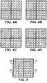
- FIG. 4A represents a two-dimensional array of pixels having two groups. Pixels from the first group of pixels have a narrower spectral photoresponse than pixels from the second group of pixels.
- the first group of pixels includes individual pixels that relate to at least two different spectral photoresponses corresponding to at least two color filters. These two groups of pixels are intermixed to improve the overall sensitivity of the sensor.
- the placement of the first and second groups of pixels defines a pattern that has a minimal repeating unit including at least twelve pixels.
- the minimal repeating unit includes first and second groups of pixels arranged to permit the reproduction of a captured color image under different lighting conditions.
- the complete pattern shown in FIG. 4A represents a minimal repeating unit that is tiled to cover an entire array of pixels.
- FIG. 2 there are several other minimal repeating units that are used to describe this overall arrangement of color and panchromatic pixels, but they are all essentially equivalent in their characteristics and each is a subarray of pixels, the subarray being eight pixels by eight pixels in extent.
- An important feature of this pattern is alternating rows of panchromatic and color pixels with the color rows having pixels with the same color photoresponse grouped together.
- the groups of pixels with the same photoresponse along with some of their neighboring panchromatic pixels are considered to form four cells that make up the minimal repeating unit, a cell being a contiguous subarray of pixels having fewer pixels than a minimal repeating unit.
- These four cells delineated by heavy lines in FIG. 4A and shown as cells 120, 122, 124, and 126 in FIG. 5 , enclose four groups of four-by-four pixels each, with 120 representing the upper left cell, 122 representing the upper right cell, 124 representing the lower left cell, and 126 representing the lower right cell.
- Each of the four cells includes eight panchromatic pixels and eight color pixels of the same color photoresponse. The color pixels in a cell are combined to represent the color for that entire cell.
- cell 120 in FIG. 5 is considered to be a green cell
- cell 122 is considered to be a red cell, and so on.
- Each cell includes at least two pixels of the same color, thereby allowing pixels of the same color to be combined to overcome the difference in photosensitivity between the color pixels and the panchromatic pixels.
- the minimal repeating unit includes sixteen pixels. In the case of a minimal repeating unit with three non-overlapping cells, with each cell having two pixels of the same color and two panchromatic pixels, it is clear that the minimal repeating unit includes twelve pixels.
- the minimal repeating unit of FIG. 4A when considered in light of the cell structure identified in FIG. 5 , can represent the combination of a high-resolution panchromatic image and a low-resolution Bayer pattern color image arranged to permit the reproduction of a captured color image under different lighting conditions.
- the individual elements of the Bayer pattern image represent the combination of the color pixels in the corresponding cells.
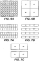
- the first group of pixels defines a low-resolution color filter array image and the second group of pixels defines a high-resolution panchromatic image. See FIG. 6A and FIG. 6B.
- FIG. 6A represents the high-resolution panchromatic image corresponding to FIG. 4A , including both the panchromatic pixels P from FIG.
- FIG. 6B represents the low-resolution Bayer pattern color image, with R', G', and B' representing for each of the cells outlined in FIG. 5 the cell color associated with the combined color pixels in the cell.
- FIGS. 4B-D are delineated by heavy lines, as they were in FIG. 4A .
- each cell of the pattern is rotated 90 degrees to produce the pattern shown in FIG. 4B .
- This is substantially the same pattern, but it places the highest panchromatic sampling frequency in the vertical direction instead of the horizontal direction.
- the choice to use FIG. 4A or FIG. 4B depends on whether or not it is desired to have higher panchromatic spatial sampling in either the horizontal or vertical directions respectively.
- FIG. 4A and FIG. 4B are equivalent from a color perspective.
- FIG. 4A and FIG. 4B are examples of practicing the present invention with the panchromatic pixels arranged linearly in either rows or columns.
- FIG. 4A has single rows of panchromatic pixels with each row separated from a neighboring row of panchromatic pixels by a row of color pixels;
- FIG. 4B has the same characteristic in the column direction.
- FIG. 4C represents yet another alternative minimal repeating unit to FIG. 4A with essentially the same cell color characteristics.
- FIG. 4C shows the panchromatic and color rows staggered on a cell by cell basis. This can improve the vertical panchromatic resolution.
- FIG. 4D Yet another alternative minimal repeating unit to FIG. 4A is represented in FIG. 4D , wherein the panchromatic and color rows are staggered by column pairs. This also has the potential of improving the vertical panchromatic resolution.
- a characteristic of all of the minimal repeating units of FIGS. 4A-D is that groups of two or more same color pixels are arranged side by side in either rows or columns.
- FIGS. 4A-D all have the same color structure with the cells that constitute the minimal repeating unit expressing a low-resolution Bayer pattern. It can therefore be seen that a variety of arrangements of panchromatic pixels and grouped color pixels are constructed within the spirit of the present invention.
- the color pixels within each cell are combined in various ways.
- the charge from same colored pixels is combined or binned in a CCD image sensor or in types of active pixel sensors that permit binning (see FIG. 1 , image sensor 20).
- the voltages corresponding to the measured amounts of charge in same colored pixels are averaged, for example by connecting in parallel capacitors that are charged to these voltages (see FIG. 1 , image sensor 20).
- the capacitors can be of equal sizes to do a simple average, or they can be of different sizes in order to do a weighted average.
- the digital representations of the light levels at same colored pixels are summed, averaged, or digitally filtered to provide a combined result, for example in FIG. 1 , digital signal processor 36.
- Combining or binning charge from two pixels doubles the signal level, while the noise associated with sampling and reading out the combined signal remains the same, thereby increasing the signal to noise ratio by a factor of two, representing a corresponding two times increase in the photosensitivity of the combined pixels.
- the resulting signal increases by a factor of two, but the corresponding noise levels from reading the two pixels combine in quadrature, thereby increasing the noise by the square root of two; the resulting signal to noise ratio of the combined pixels therefore increases by the square root of two over the uncombined signals.
- a similar analysis applies to voltage or digital averaging.
- each R', G', and B' has twice the sensitivity of the uncombined pixels.
- vertically combining the charge from same colored pixels in groups of two as in FIG. 7A and horizontally summing or averaging the measured values of the combined pixels of FIG. 7A in groups of four produces the final combined color pixels of FIG. 7C , with R", G", and B" representing the final combinations of same colored pixels.
- the final combined color pixels of FIG. 7C each have four times the sensitivity of the uncombined pixels.
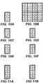
- FIG. 8A shows a rotated form of the minimal repeating unit of FIG. 8A .
- FIG. 9A shows a variation of minimal repeating of FIG. 8A that uses four colors in addition to the panchromatic pixels.
- FIGS. 9B-C show additional variations of both of these patterns in which the single row of panchromatic pixels is replaced by a double row of panchromatic pixels. All of these patterns do not have a plurality of pixels of the same color. This fact and the preferred method for using such patterns will be discussed later.
- FIG. 10A Another minimal repeating unit is shown in FIG. 10A that contains one red, two green, and one blue pixels.
- FIG. 10B A tiling example, using this pattern, is shown in FIG. 10B .
- FIG. 10C shows the cyan, magenta, and yellow equivalent of FIG. 10A , with C representing cyan pixels, M representing magenta pixels, and Y representing yellow pixels.
- FIG. 10D shows a minimal repeating unit of the present invention that includes cyan pixels (represented by C), magenta pixels (represented by M), yellow pixels (represented by Y), and green pixels (represented by G).
- FIG. 10E shows yet another alternative four color arrangement including red pixels (represented by R), blue pixels (represented by B), green pixels with one color photoresponse (represented by G), and alternative green pixels with a different color photoresponse (represented by E).
- FIG. 10F shows yet another alternative four color arrangement, wherein one of the green cells of FIG. 10A is replaced by a yellow cell, with the yellow pixels represented by Y.
- FIG. 11A shows a variation of the pattern of FIG. 10A in which each row of panchromatic pixels is replaced by a double row of panchromatic pixels.
- An additional example, shown in FIG. 11B is the same variation applied to the pattern of FIG. 10E .
- FIG.12A shows a variation of the pattern of FIG. 8A in which the pixels are octagonal and are arranged on a diagonal row. Because the pixel geometry is octagonal, there are small square vacancies located between horizontal and vertical neighbors that can be used for required sensor functionality such as data transfer circuitry.
- FIG. 12B shows an example of a tiling pattern using the minimal repeating unit of FIG. 12A . In FIG. 12B the panchromatic pixels appear in rows that are diagonal in nature. Likewise, the color pixels also appear in diagonally oriented rows.
- FIG. 13A shows another variation of the pattern of FIG. 8A in which the pixels are hexagonal and arranged vertically.
- FIG. 13B shows an example of a tiling pattern using the minimal repeating unit of FIG. 13A .
- the panchromatic pixels appear in columns.
- the color pixels also appear in columns.
- FIG. 14 shows another minimal repeating unit using fewer panchromatic pixels than color pixels wherein the pixels are hexagonally packed and wherein the panchromatic pixels appear in rows that are diagonal in nature. Also, in FIG. 14 , the color pixels appear in diagonally oriented rows.
- FIG. 15 shows another variation of the pattern of FIG. 13A . Within the scope of the present invention, it should be noted that rows and columns of pixels are not necessarily perpendicular to each other as is shown in FIGS. 12A-15 .
- FIG. 16 the minimal repeating unit of FIG. 5 is shown subdivided into four cells, a cell being a contiguous subarray of pixels having fewer pixels than a minimal repeating unit.
- the software needed to provide the following processing is included in DSP 36 of FIG. 1 .
- Cells 220, 224, 226, and 228 are examples of cells wherein these cells contain pixels having green, red, blue and green photoresponses, respectively.
- cell 220 contains both panchromatic pixels and green pixels, the green pixels being identified as pixel group 222.
- the eventual goal is to produce a single green signal for cell 220 by combining the eight green signals from the green pixels in pixel group 222.
- a single green signal is produced by combining all eight green signals in the analog domain (e.g. by charge binning), or multiple green signals are produced by combining smaller groups of pixels taken from pixel group 222.
- the panchromatic pixels of cell 220 are shown in FIG. 17A . In the following examples, all eight signals from these panchromatic pixels are individually digitized.
- the green pixels of cell 220 are shown in FIGS. 17B-17E wherein they are grouped together according to how their signals are combined.
- FIG. 17B depicts the case in which all eight green pixels are combined to produce a single green signal for cell 220 ( FIG. 16 ).
- the sensor can produce two green signals, for example, by first combining the signals from pixels G21, G22, G23, and G24, and then combining the signals from pixels G41, G42, G43, and G44, as shown in FIG. 17C .
- Two signals are produced in other ways as well.
- the sensor can first combine signals from pixels G21, G22, G41, and G42, and then combine signals from pixels G23, G24, G43, and G44, as shown in FIG. 17D .
- the sensor can also produce four green signals for cell 220 by combining four pairs of signals, for example, combining pixels G21 with G22, then combining G23 with G24, then combining G41 with G42, and finally combining G43 with G44, as shown in FIG. 17E .
- cells 224, 226, and 228 For cells 224, 226, and 228 ( FIG 16 ), similar color signals are produced by the sensor depending on its mode of operation.
- the color signals for cells 224, 226, and 228 are red, blue, and green, respectively.
- the image processing algorithm of the present invention further combines the digitized green values to produce a single green value for the cell.
- One way that a single green value is obtained is by averaging all the digitized green values produced for cell 220.
- all the color data within the cell is similarly combined so that there is a single value for each color photoresponse represented within the cell.
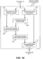
- the digital signal processor block 36 ( FIG. 1 ) is shown receiving captured raw image data from the data bus 30 ( FIG. 1 ).
- the raw image data is passed to both the Low-resolution Partial Color block 202 and the High-resolution Panchrome block 204.
- An example of a minimal repeating unit for an image sensor has already been shown in FIG. 5 and FIG. 16 .
- the captured raw image data includes the panchromatic data that is produced by the individual panchromatic pixels as shown in FIG 17A .
- one or more green (color) values are also included, for example, from the combinations shown in FIGS. 17B-E .
- a partial color image is produced from the captured raw image data, a partial color image being a color image wherein each pixel has at least one color value and each pixel is also missing at least one color value.
- the captured raw data contains some number of color values produced by the color pixels within each cell.
- these color values are reduced to a single value for each color represented within the cell. For the cell 220 ( FIG. 16 ), as an example, a single green color value is produced.
- cells 224, 226 and 228, a single red, blue and green color value is produced, respectively.
- the Low-resolution Partial Color block 202 processes each cell in a similar manner resulting in an array of color values, one for each cell. Because the resulting image array is based on cells rather than pixels in the original sensor, it is four times smaller in each dimension than the original captured raw image data array. Because the resulting array is based on cells and because each pixel has some but not all color values, the resulting image is a low-resolution partial color image. At this point, the low-resolution partial color image is color balanced.
- panchromatic values must be estimated for the green pixels in pixel group 222 ( FIG. 16 ).
- panchromatic value is to do vertical averaging.
- we can estimate the panchromatic value at pixel 22 as follows: P 22 P 12 + P 32 / 2
- an adaptive method can also be used.
- panchromatic interpolation is continued throughout the image without regard to cell boundaries.
- the processing of High-resolution Panchrome block 204 is done, the resulting digital panchromatic image is the same size as the original captured raw image, which makes it a high-resolution panchromatic image.
- the Low-resolution Panchrome block 206 receives the high-resolution panchromatic image array produced by block 204 and generates a low-resolution panchromatic image array which is the same size as the low-resolution partial color image produced by block 202.
- Each low-resolution panchromatic value is obtained by averaging the estimated panchromatic values, within a given cell, for those pixels having color filters.
- the high-resolution panchromatic values previously estimated for the green pixels in pixel group 222 ( FIG. 16 ) are now averaged together to produce a single low-resolution panchromatic value for the cell.
- a single low-resolution panchromatic value is computed for cell 224 using high-resolution panchromatic values estimated at the pixels having red filters. In this manner, each cell ends up with a single low-resolution panchromatic value.
- the Low-resolution Color Difference block 208 receives the low-resolution partial color image from block 202 and the low-resolution panchrome array from block 206. A low-resolution intermediate color image is then formed by color interpolating the low-resolution partial color image with guidance from the low-resolution panchrome image. The exact nature of the color interpolation algorithm, to be discussed in detail later, depends on which pattern of pixel photoresponses was used to capture the original raw image data.
- the High-resolution Color Difference block 210 receives the low-resolution color difference image from block 208 and, using bilinear interpolation, upsamples the low-resolution color difference image to match the size of the original raw image data. The result is a high-resolution color difference image that is the same size as the high-resolution panchromatic image produced by block 204.
- the High-resolution Final Image block 212 receives the high-resolution color difference image from block 210 and the high-resolution panchromatic image from block 204.
- a high-resolution final color image is then formed by adding the high-resolution panchromatic image to each of the high-resolution color difference planes.
- the resulting high-resolution final color image can then be further processed. For example, it is stored in the DSP Memory block 32 ( FIG. 1 ) and then sharpened and compressed for storage on the Memory Card block 64 ( FIG. 1 ).
- the sensor filter patterns shown in FIGS. 4A-D have a minimal repeating unit such that the resulting low-resolution partial color image, produced in block 202, exhibits the repeating Bayer pattern for color filters: G R B G
- every cell In addition to a single color value, given by the low-resolution partial color image, every cell also has a panchromatic value given by the low-resolution panchromatic image.
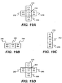
- Color interpolation begins by interpolating the green values at pixels not already having green values, shown as pixel 234 in FIG. 19A .
- the four neighboring pixels shown as pixels 230, 232, 236, and 238, all have green values and they also all have panchromatic values.
- the center pixel 234 has a panchromatic value, but does not have a green value as indicated by the question marks.
- the first step is to compute two classifier values, the first relating to the horizontal direction, and the second to the vertical direction:
- HCLAS ABS P 4 ⁇ P 2 + ABS 2 * P 3 ⁇ P 2 ⁇ P 4
- VCLAS ABS P5 ⁇ P 1 + ABS 2 * P 3 ⁇ P 1 ⁇ P 5
- THRESH be an empirically determined threshold value
- red and blue values are interpolated.
- pixel 242 is missing a red value but its two horizontal neighbors, pixels 240 and 244, have red values R2 and R4 respectively. All three pixels have green values.
- Missing blue values are computed in a similar way under similar conditions. This completes the interpolation of the low-resolution partial color image and the result is a low-resolution intermediate color image. As described earlier, the low-resolution color differences can now be computed by subtracting the low-resolution panchrome values from each color plane: red, green, and blue in the example just discussed.
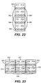
- FIG. 20 a partial tiling of a sensor is shown using four copies of the minimal repeating unit of FIG. 8A .
- the four minimal repeating units 310, 311, 312, and 313 each contain a red, green, and blue pixel.
- the present invention can also be practiced by combining pixels from nearby minimal repeating units.
- the red pixels R21 and R41 constitute a pair of pixels 314 that are combined in a vertical direction.
- the green pixels G42 and G45 constitute a pair of pixels 315 that are combined in a horizontal direction.
- the minimal repeating is relatively small, such as the pattern of FIG. 8A as used in FIG. 20 , it is useful to combine like colored pixels from adjacent minimal repeating units.
- similarly positioned pixels from adjacent minimal repeating units are combined, where similarly positioned is defined as having the same relative position within each minimal repeating unit.
- similarly positioned pixels For example, pixels G42 and G45 in FIG. 20 are similarly positioned and are combined as pair 315. Note that similarly positioned pixels must be pixels of like color.
- panchromatic pixels P12 and P15 in FIG. 20 are similarly positioned and are combined as the pair 316.
- panchromatic pixels P13 and P14 are pixels of like color (but are not similarly positioned) and are combined as the pair 317.
- panchromatic pixels P35 and P36 are pixels of like color within a minimal repeating unit that are combined as the pair 318.
- the combining that has been described to this point includes combining pixels of like color or similarly positioned pixels from adjacent minimal repeating units. In some cases, it is useful to combined panchromatic pixels with color pixels.
- the combined pair 319 includes panchromatic pixel P16 and blue pixel B26. Combining panchromatic with color pixels is done, for example, when the light level is low or the exposure time is very short in order to increase the overall signal strength from the combined pixels.
- 319 shows the combination of a panchromatic pixel and a color pixel from within one minimal repeating unit, it is also useful to combine panchromatic pixels with color pixels from nearby minimal repeating units.
- FIGS. 21 through 27 Examples of the various combining methods described above are shown in FIGS. 21 through 27 .
- FIGS. 21A-21D two adjacent minimal repeating units 330 and 331 that are a variation of the type shown in FIG. 10A are shown.
- FIG. 21A all similarly positioned color pixels from the two minimal repeating units are combined as shown by pixel pairs 332, 333, 334, and 335.
- FIG. 21B all similarly positioned panchromatic pixels are combined as shown by pixels pairs 336, 337, 338, and 339.
- FIG. 21C shows combining pixels of like color within a minimal repeating unit at the same time as combining similarly positioned pixels between minimal repeating units.
- FIG. 21C includes two adjacent minimal repeating units 330 and 331 that are a variation of the type shown in FIG. 10A .
- positioned pixels R21 and R23 are combined as the pair 340
- similarly positioned pixels B42 and B44 are combined as the pair 341.
- G22 and G41 are pixels of like color that are located in minimal repeating unit 330, and they are shown combined as the pair 342; similarly, pixels G24 and G43 from minimal repeating unit 331 are shown combined as the pair 343.
- FIG. 21D shows combining panchromatic pixels within a minimal repeating unit at the same time as combining panchromatic pixels between minimal repeating units.
- FIG. 21D includes two adjacent minimal repeating units 330 and 331 that are a variation of the type shown in FIG. 10A .
- P11 and P12 are panchromatic pixels that are located in minimal repeating unit 330, and they are shown combined as the pair 344; similarly, pixels P13 and P14 from minimal repeating unit 331 are shown combined as the pair 345.
- Panchromatic pixels P32 and P33 are in different minimal repeating units, and they are shown combined as the pair 346. Uncombined panchromatic pixels P31 and P34 are left uncombined or are combined with pixels from adjacent minimal repeating units as shown by the arrows 347 and 348.
- FIG. 22 shows two adjacent minimal repeating units 360 and 361 that are arranged vertically, with similarly positioned color pixels combined as shown by pixel pairs 362, 363, 364, and 365.
- FIG. 23 shows three adjacent minimal repeating units 370, 371, and 372 that are a variation of the type shown in FIG. 10A . Pixels of like color (that are also similarly positioned) are shown combined in threes as the pixel triplets 373, 374, 375, and 376.
- FIG. 24 shows five adjacent minimal repeating units 380, 381, 382, 383, and 384 that are a variation of the type shown in FIG. 10A with pixels of like color shown combined as red triplet 390, green pair 391, green triplet 392, red pair 393, green triplet 394, blue pair 395, blue triplet 396, and green pair 397.
- This particular arrangement produces combined pixel pairs that are evenly spaced.
- Combination 390 produces a combined red result that is located at the position of R23 (assuming pixels R21, R23, and R25 are equally weighted in the combining process), and combination 391 produces a combined green result that is located also at the position of R23.
- Pixel positions R23, G28, G43, and B48 are evenly spaced within the group of five minimal repeating units and, if this group of five minimal repeating units and combined pixels is repeated to create a larger array of minimal repeating units, the resulting combined pixels are evenly spaced throughout the resulting array. Contrast this with the combining arrangement shown in FIG. 23 : if this group of three minimal repeating units and combined pixels is repeated to create a larger array, the resulting combined pixels are concentrated in the center of each group of three minimal repeating units and are therefore not spaced evenly throughout the array.
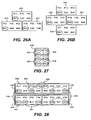
- FIG. 25A shows four adjacent minimal repeating units 400, 401, 402, and 403 that are a variation of the type shown in FIG. 10A .
- some pixels of like color are combined within the group of four minimal repeating units, while other pixels are combined with pixels from minimal repeating units that are adjacent to this group of four.
- pixels R21, R23, and R25 are combined as the triplet 410
- pixels G24, G26, and G28 are combined as the triplet 411
- pixels G41, G43, and G45 are combined as the triplet 412
- pixels B44, B46, and B48 are combined as the triplet 413.
- pixels G22 is combined with pixels from minimal repeating units to the left of the group of four as shown by arrow 414.
- pixel B42 is combined with pixels from adjacent minimal repeating units to the left as shown by the arrow 416
- pixels R27 and G47 are combined with pixels from adjacent minimal repeating units to the right as shown by arrows 415 and 417, respectively.
- FIG. 25A If a minimal repeating unit of the type exemplified by 400 through 403 in FIG. 25A is tiled to create a larger array, the combining arrangement shown in FIG. 25A is extended to cover an array of minimal repeating units as shown in FIG. 25B .
- FIG. 25B In FIG. 25B are shown three overlapping groups of four minimal repeating units: 405L, 405C, and 405R.
- Group 405L is composed of minimal repeating units 400L, 401L, 402L, and 403L that correspond for combining purposes to minimal repeating units 400, 401, 402, and 403 respectively of FIG. 25A .
- group 405C is composed of minimal repeating units 400C, 401C, 402C, and 403C that also correspond to minimal repeating units 400, 401, 402, and 403 of FIG. 25A
- group 405R is composed of minimal repeating units 400R, 401R, 402R, and 403R that also correspond to minimal repeating units 400, 401, 402, and 403 of FIG. 25A
- minimal repeating unit 403L of group 405L is also minimal repeating unit 400C of group 405C
- minimal repeating unit 403C of group 405C is also minimal repeating unit 400R of group 405R.
- minimal repeating unit 403L/400C is where groups 405L and 405C overlap
- minimal repeating unit 403C/400R is where groups 405C and 405R overlap.
- the curved lines contained within each group of four minimal repeating units, 405L, 405C, and 405R connect the pixels that are combined as shown by 410, 411, 412, and 413 in FIG. 25A .
- the curved lines that extend outside a group connect to an adjacent and overlapping group and correspond to 414, 415, 416, and 417 in FIG. 25A .
- FIGS. 25A and 25B provides combined results for the color pixels that are evenly spaced.
- the combined color pixels represent a Bayer arrangement of colors.
- the minimal repeating unit is the tiling unit that is used to create larger arrays of pixels.
- the groups of minimal repeating units shown in FIGS. 24, 25A, and 25B are for combining purposes only, not for tiling purposes. In some cases the combining is contained entirely within the group of minimal repeating units, as shown in FIG. 24 , and in some cases the combining extends outside the group as shown in FIG. 25A . In some cases where the combining extends outside a group of minimal repeating units, representative groups of minimal repeating units are overlapped for combining purposes as shown in FIG. 25B .
- minimal repeating units are grouped in one arrangement for combining some pixels, and are group in another arrangement for combining other pixels. For example, minimal repeating units are grouped in one arrangement to combine color pixels and are grouped in a different arrangement to combine panchromatic pixels.
- FIG. 20 provides one such example in which four minimal repeating units are arranged in two rows and two columns.
- FIG. 26A Another example is shown in FIG. 26A , which has three minimal repeating units 420, 421, and 422 of the type shown in FIG. 8A .
- the three minimal repeating units are arranged so that each minimal repeating unit is adjacent to the others. Pixels of similar color within this group of three are combined: for example, pixels R21, R41, and R44 are combined. This arrangement of three mutually adjacent minimal repeating units is repeated to produce a larger array of pixels.
- FIG. 26B has four minimal repeating units 425, 426, 427, and 428 of the type shown in FIG. 8A , with each of the four minimal repeating units adjacent to at least two others within the group of four. Pixels of similar color with this group of four are combined: for example, pixels R21, R41, R44, and R61 are combined.
- FIG. 27 shows combining panchromatic pixels with color pixels.
- Minimal repeating unit 430 is a variation of the type shown in FIG. 10A .
- Pixels P11 and R21 form the combined pair 431
- pixels P12 and G22 form the combined pair 432
- pixels P31 and G41 form the combined pair 433
- pixels P32 and B42 form the combined pair 434.
- FIG. 28 a minimal repeating unit having 16 pixels is shown having two copies, minimal repeating units 440 and 441.
- the top minimal repeating unit 440 is subdivided into two cells 442 and 443.
- Cell 442 contains a horizontal row of four panchromatic pixels P11, P12, P13, and P14, two blue pixels B21 and B23, and two green pixels G22 and G24.
- Cell 443 contains a horizontal row of four panchromatic pixels P15, P16, P17, and P18, two red pixels R25 and R27 and two green pixels G26 and G28.
- the bottom minimal repeating unit 441 is subdivided into two cells 444 and 445 that contain similar patterns of pixels as cells 442 and 443, respectively.
- pixels B21 and B41 from adjacent minimal repeating units 440 and 441 provide the combined pixel pair 450.
- Pixels G42 and G44 from the cell 444 provide the combined pixel pair 451.
- Pixels P14 and P15 are panchromatic pixels from cells 442 and 443 respectively that provide the pixel pair 452.
- Panchromatic pixel P13 is combined with color pixel B23 to provide the combined pixel pair 453.
- the present invention includes combining an arbitrary number of pixels, both within a single minimal repeating unit and among multiple adjacent minimal repeating units.
- the green pixels G26, G28, G46, and G48 constitute a four-tuple of combined pixels 455 all of which are combined to produce a single color value.
- This fourfold combination simultaneously includes combining pixels horizontally and vertically, as well as combining a plurality of pixels from within a single minimal repeating unit, and pixels taken from multiple adjacent minimal repeating units.
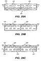
- FIGS. 29A-C shows a minimal repeating unit 460 of the type shown in FIG. 28 .
- the minimal repeating unit 460 is composed of two cells, 462 and 464.
- pixels B21 and B23 from within cell 462 provide the combined pixel pair 465.
- pixels R25 and R27 from within cell 464 provide the combined pixel pair 466.
- the red and blue combined pixels are contained entirely within their respective cells, while the green combined pixels come from two different cells.
- This particular combining arrangement has an advantage with respect to placement of the combined results: the centroid of the combined blue pixel pair 465 is at the position of pixel G22, the centroid of the combined green pixel triplet 467 is at the position of pixel G24, the centroid of the combined red pixel pair 466 is at the position of pixel G26, while the uncombined green pixel G28 remains at its current position.
- the combined color pixels' centroids along with the uncombined green pixel are evenly spaced, thereby minimizing aliasing in the sampling process.
- FIG. 29B shows combining panchromatic pixels from within the cells of minimal repeating unit 460.
- Panchromatic pixels P11, P12, and P13 provide the combined pixel triplet 468
- panchromatic pixels P15, P16, and P17 provide the combined pixel triplet 469.
- the combining arrangement of FIG. 29B has an advantage with respect to placement of the combined results: the centroid of the combined pixel triplet 468 is at the position of pixel P12, the centroid of the combined pixel triplet 469 is at the position of pixel P16, while the uncombined panchromatic pixels P14 and P18 remain at their current positions.
- the combined panchromatic pixels' centroids along with the uncombined panchromatic pixels are evenly spaced. Furthermore, these evenly spaced combined and uncombined panchromatic pixels are arranged vertically above the corresponding combined and uncombined color pixels shown in FIG. 29A , potentially simplifying the interpolation process.
- FIG. 29C shows additional combinations of panchromatic pixels: pixels P13 and P14 from cell 462 are combined with pixel P15 from cell 464 to provide the combined panchromatic triplet 470; pixels P17 and P18 from cell 464 are combined with the leftmost pixel from a minimal repeating unit to the right of minimal repeating unit 460 to form the combined panchromatic pixel triplet 471; and pixel P11 from cell 462 is combined with the rightmost two panchromatic pixels from a minimal repeating unit to the left of minimal repeating unit 460 to form the combined panchromatic pixel triplet 472.
- the four combined panchromatic pixel triplets in FIG. 29C have their centroids evenly spaced.
- Pixel P11 is used twice, once in combination 472 and once in combination 468; pixel P13 is used in combinations 468 and 470; pixel P15 is used in combinations 470 and 469, and pixel P17 is used in combinations 469 and 471.
- the sensor pattern shown in FIG. 28 and FIGS. 29A-C determines that two adjacent minimal repeating units generate two pairs of color values.
- a pair of cells from adjacent minimal repeating units produces color values for a low-resolution color representation of the image.
- the pair of cells 442 and 444 provide a blue and a green color value by combining pixels B21, B23, B41, and B43 for the blue value and by combining pixels G22, G24, G42, and G44 for the green value.
- the pair of cells 443 and 445 provide a red and a green color value by combining pixels R25, R27, R45, and R47 for the red value and by combining pixels G26, G28, G46, and G48 for the green value.
- This pattern of combining pixels between cells from adjacent minimal repeating units is repeated over the entire sensor.
- the result is a low-resolution representation of the image wherein each low-resolution pixel has a green color value and either a red or a blue color value.
- the color interpolation task within the Low-resolution Color Differences block 208 estimates missing values of red or missing values of blue for each pixel. Referring to FIG.
- a pixel 264 is shown having a green value (G3) but not having a red value (R3).
- G3 green value
- R3 red value
- Four of the neighboring pixels 260, 262, 266, and 268 have green values and red values.
- the method for interpolating the red value for pixel 264 ( FIG. 19D ) is similar to the method used to interpolate the green value for pixel 234 ( FIG. 19A ).
- the first step is to compute two classifier values, the first relating to the horizontal direction, and the second to the vertical direction:
- HCLAS ABS G 4 ⁇ G 2 + ABS 2 * G 3 ⁇ G 2 ⁇ G 4
- VCLAS ABS G 5 ⁇ G 1 + ABS 2 * G 3 ⁇ G 1 ⁇ G 5
- HPRED R 4 + R 2 / 2 + 2 * G 3 ⁇ G 2 ⁇ G 4 / 2
- the missing value G3 is computed adaptively according to:
- the missing blue values are interpolated in exactly the same way using blue values in place of red.
- the low-resolution intermediate color image has been produced. From there, the low-resolution color differences are computed as previously described.
Landscapes
- Engineering & Computer Science (AREA)
- Multimedia (AREA)
- Signal Processing (AREA)
- Physics & Mathematics (AREA)
- Spectroscopy & Molecular Physics (AREA)
- Color Television Image Signal Generators (AREA)
- Solid State Image Pick-Up Elements (AREA)
Description
- This invention relates to a two-dimensional image sensor with improved light sensitivity.
- An electronic imaging system depends on an electronic image sensor to create an electronic representation of a visual image. Examples of such electronic image sensors include charge coupled device (CCD) image sensors and active pixel sensor (APS) devices (APS devices are often referred to as CMOS sensors because of the ability to fabricate them in a Complementary Metal Oxide Semiconductor process). Typically, these image sensors include a number of light sensitive pixels, often arranged in a regular pattern of rows and columns. For capturing color images, a pattern of filters is typically fabricated on the pattern of pixels, with different filter materials being used to make individual pixels sensitive to only a portion of the visible light spectrum. The color filters necessarily reduce the amount of light reaching each pixel, and thereby reduce the light sensitivity of each pixel. A need persists for improving the light sensitivity, or photographic speed, of electronic color image sensors to permit images to be captured at lower light levels or to allow images at higher light levels to be captured with shorter exposure times.
- Image sensors are either linear or two-dimensional. Generally, these sensors have two different types of applications. The two-dimensional sensors are typically suitable for image capture devices such as digital cameras, cell phones and other applications. Linear sensors are often used for scanning documents. In either case, when color filters are employed the image sensors have reduced sensitivity.
- A linear image sensor, the KLI-4104 manufactured by Eastman Kodak Company, includes four linear, single pixel wide arrays of pixels, with color filters applied to three of the arrays to make each array sensitive to either red, green, or blue in its entirety, and with no color filter array applied to the fourth array; furthermore, the three color arrays have larger pixels to compensate for the reduction in light sensitivity due to the color filters, and the fourth array has smaller pixels to capture a high resolution monochrome image. When an image is captured using this image sensor, the image is represented as a high resolution, high photographic sensitivity monochrome image along with three lower resolution images with roughly the same photographic sensitivity and with each of the three images corresponding to either red, green, or blue light from the image; hence, each point in the electronic image includes a monochrome value, a red value, a green value, and a blue value. However, since this is a linear image sensor, it requires relative mechanical motion between the image sensor and the image in order to scan the image across the four linear arrays of pixels. This limits the speed with which the image is scanned and precludes the use of this sensor in a handheld camera or in capturing a scene that includes moving objects.
- There is also known in the art an electronic imaging system described in
US Patent 4,823,186 by Akira Muramatsu that includes two sensors, wherein each of the sensors includes a two-dimensional array of pixels but one sensor has no color filters and the other sensor includes a pattern of color filters included with the pixels, and with an optical beam splitter to provide each image sensor with the image. Since the color sensor has a pattern of color filters applied, each pixel in the color sensor provides only a single color. When an image is captured with this system, each point in the electronic image includes a monochrome value and one color value, and the color image must have the missing colors at each pixel location interpolated from the nearby colors. Although this system improves the light sensitivity over a single conventional image sensor, the overall complexity, size, and cost of the system is greater due to the need for two sensors and a beam splitter. Furthermore, the beam splitter directs only half the light from the image to each sensor, limiting the improvement in photographic speed. - In addition to the linear image sensor mentioned above, there are known in the art image sensors with two-dimensional arrays of pixels where the pixels include pixels that do not have color filters applied to them. For example, see
Sato, et al. in US Patent 4,390,895 ,Yamagami, et al. in US Patent 5,323,233 , andGindele, et al. in US Patent 6,476,865 . In each of the cited patents, the sensitivity of the unfiltered or monochrome pixels is significantly higher than the color pixels, requiring the application of gain to the color pixels in order to match the color and monochrome signals from the pixel array. Increasing gain increases noise as well as signal, causing degradation in the overall signal to noise ratio of the resulting image.Frame in US Patent Application 2003/0210332 discloses a pixel array with most of the pixels being unfiltered, but the color pixels suffer from the same sensitivity deficit as mentioned above. - Therefore, there persists a need for improving the light sensitivity for electronic capture devices that employ a single sensor with a two-dimensional array of pixels.
-
EP1594321 discloses a digital color imager providing an extended luminance range, an improved color implementation and enabling a method for an easy transformation into another color space having luminance as a component has been achieved. -
US2005/0068426 discloses a solid-state imaging element which includes photoelectric conversion elements having a complementary or Bayer color filter array. -
US4246600 discloses a color image pickup system for a color television system which comprises a single image pickup device and a color filter mounted in front of the screen of said image pickup device. -
JP62-038692 -
EP0049594 discloses a color image pick-up apparatus using a single planar array of solid state light-sensitive elements with a color mosaic filter. - The present invention is directed to providing an image sensor having a two-dimensional array of color and panchromatic pixels that provides high sensitivity and is effective in producing full color images.
- Briefly summarized, according to one aspect of the present invention, there is provided an image sensor as set out in
claim 1. Further aspects of the present invention are set out in the remaining claims. - Image sensors in accordance with the present invention are particularly suitable for low level lighting conditions, where such low level lighting conditions are the result of low scene lighting, short exposure time, small aperture, or other restriction on light reaching the sensor. They have a broad application and numerous types of image capture devices can effectively use these sensors.
- These and other aspects, objects, features and advantages of the present invention will be more clearly understood and appreciated from a review of the following detailed description of the preferred embodiments and appended claims, and by reference to the accompanying drawings.
-
-
FIG. 1 is a block diagram of a conventional digital still camera system that can employ a conventional sensor and processing methods or the sensor and processing methods of the current invention; -
FIG. 2 (prior art) is a conventional Bayer color filter array pattern showing a minimal repeating unit and a non-minimal repeating unit; -
FIG. 3 provides representative spectral quantum efficiency curves for red, green, and blue pixels, as well as a wider spectrum panchromatic quantum efficiency, all multiplied by the transmission characteristics of an infrared cut filter; -
FIGS. 4A-D provides minimal repeating units for several variations of a color filter array pattern of the present invention that has color pixels with the same color photo response arranged in rows or columns; -
FIG. 5 shows the cell structure of the minimal repeating unit fromFIG. 4A ; -
FIG. 6A is the interpolated panchromatic image forFIG. 4A ; -
FIG. 6B is the low-resolution color image corresponding to the cells inFIG. 4A and FIG. 5 ; -
FIGS. 7A-C shows several ways of combining the pixels ofFIG. 4A ; -
FIGS. 8A-E provides a minimal repeating unit of six pixels for a color filter array pattern of the present invention including several tiling arrangements and an alternative orientation for the minimal repeating unit; -
FIG. 9A-C provides several minimal repeating units for color filter array patterns of the present invention that are variants of the minimal repeating unit ofFIG. 8 ; -
FIGS. 10A-F provides a minimal repeating unit of eight pixels for a color filter array pattern of the present invention and includes a tiling arrangement and variations with color pixels that have alternative color photoresponse characteristics, including primary color, complementary color, three color, and four color alternatives; -
FIGS. 11A-B provides a minimal repeating unit for a color filter array of the present invention in which more than half the pixels have a panchromatic photoresponse; -
FIGS. 12A-B provides a minimal repeating unit for a color filter array of the present invention in which the pixels are on a rectangular grid that is rotated forty-five degrees, and includes a tiling arrangement; -
FIGS. 13A-B provides a minimal repeating unit for a color filter array of the present invention in which the pixels are arranged in a hexagonal pattern, and includes a tiling arrangement; -
FIGS. 14 provides a minimal repeating unit for a color filter array of the present invention that is an alternative toFIG. 13 ; -
FIGS. 15 provides a minimal repeating unit for a color filter array of the present invention that is an alternative toFIG. 13 ; -
FIG. 16 is the minimal repeating unit ofFIG. 4A with subscripts for individual pixels within the minimal repeating unit; -
FIGS. 17A-E shows the panchromatic pixels and the color pixels of one cell ofFIG. 16 , and various ways in which the color pixels are combined; -
FIG. 18 is a process diagram of the present invention showing the method of processing the color and panchromatic pixel data from a sensor of the present invention; -
FIGS. 19A-D illustrates methods of the present invention for interpolating missing colors in the low-resolution partial color image ofFIG. 18 ; -
FIG. 20 provides two minimal repeating units of the type shown inFIG. 8A showing combining pixels between adjacent minimal repeating units as well as within the minimal repeating units; -
FIGS. 21A-D each provide two minimal repeating units that are a variant ofFIG. 10A showing several ways of combining pixels between horizontally adjacent minimal repeating units and within minimal repeating units; -
FIG. 22 provides two minimal repeating units that are a variant ofFIG. 10A showing combining pixels between vertically adjacent minimal repeating units; -
FIG. 23 provides three minimal repeating units that are a variant ofFIG. 10A showing combining pixels from three horizontally adjacent minimal repeating units; -
FIG. 24 provides five minimal repeating units that are a variant ofFIG. 10A showing combining pixels from five horizontally adjacent minimal repeating units; -
FIGS. 25A-B provides several minimal repeating units that are a variant ofFIG. 10A showing multiple overlapping groups of minimal repeating units for the purpose of combining pixels from adjacent minimal repeating units; -
FIGS. 26A-B provides several minimal repeating units of the type shown inFIG. 8A showing combining pixels from multiple mutually adjacent minimal repeating units; -
FIG. 27 provides a minimal repeating unit that is a variant ofFIG. 10A showing combining color pixels with panchromatic pixels; -
FIG. 28 provides two minimal repeating units that are a variation of the present invention that include cells showing combining pixels between minimal repeating units, between cells, and within cells, as well as combining color and panchromatic pixels; and -
FIGS. 29A-C provides a minimal repeating unit that is a variation of the present invention that includes cells showing specific examples of combining pixels between minimal repeating units, between cells, and within cells. - Because digital cameras employing imaging devices and related circuitry for signal capture and correction and for exposure control are well known, the present description will be directed in particular to elements forming part of, or cooperating more directly with, method and apparatus in accordance with the present invention. Elements not specifically shown or described herein are selected from those known in the art. Certain aspects of the embodiments to be described are provided in software. Given the system as shown and described according to the invention in the following materials, software not specifically shown, described or suggested herein that is useful for implementation of the invention is conventional and within the ordinary skill in such arts.
- Turning now to
FIG. 1 , a block diagram of an image capture device shown as a digital camera embodying the present invention is shown. Although a digital camera will now be explained, the present invention is clearly applicable to other types of image capture devices. In the disclosed camera, light 10 from the subject scene is input to animaging stage 11, where the light is focused bylens 12 to form an image on solidstate image sensor 20.Image sensor 20 converts the incident light to an electrical signal for each picture element (pixel). Theimage sensor 20 of the preferred embodiment is a charge coupled device (CCD) type or an active pixel sensor (APS) type (APS devices are often referred to as CMOS sensors because of the ability to fabricate them in a Complementary Metal Oxide Semiconductor process). Other types of image sensors having two-dimensional array of pixels are used provided that they employ the present invention. The present invention also makes use of animage sensor 20 having a two-dimensional array of color and panchromatic pixels as will become clear later in this specification afterFIG. 1 is described. Examples of the patterns of color and panchromatic pixels of the present invention that are used with theimage sensor 20 are seen inFIGS. 4A-D ,FIG. 8A, FIG.8E, FIGS. 9A-C ,FIG. 10A, FIGS. 10C-F, FIGS. 11A-B ,FIG. 12, FIG. 13, FIG. 14, and FIG. 15 , although other patterns are used within the spirit of the present invention. - The amount of light reaching the
sensor 20 is regulated by aniris block 14 that varies the aperture and the neutral density (ND)filter block 13 that includes one or more ND filters interposed in the optical path. Also regulating the overall light level is the time that theshutter block 18 is open. Theexposure controller block 40 responds to the amount of light available in the scene as metered by thebrightness sensor block 16 and controls all three of these regulating functions. - This description of a particular camera configuration will be familiar to one skilled in the art, and it will be obvious that many variations and additional features are present. For example, an autofocus system is added, or the lenses are detachable and interchangeable. It will be understood that the present invention is applied to any type of digital camera, where similar functionality is provided by alternative components. For example, the digital camera is a relatively simple point and shoot digital camera, where the
shutter 18 is a relatively simple movable blade shutter, or the like, instead of the more complicated focal plane arrangement. The present invention can also be practiced on imaging components included in non-camera devices such as mobile phones and automotive vehicles. - The analog signal from
image sensor 20 is processed byanalog signal processor 22 and applied to analog to digital (A/D)converter 24. Timinggenerator 26 produces various clocking signals to select rows and pixels and synchronizes the operation ofanalog signal processor 22 and A/D converter 24. Theimage sensor stage 28 includes theimage sensor 20, theanalog signal processor 22, the A/D converter 24, and thetiming generator 26. The components ofimage sensor stage 28 are separately fabricated integrated circuits, or they are fabricated as a single integrated circuit as is commonly done with CMOS image sensors. The resulting stream of digital pixel values from A/D converter 24 is stored inmemory 32 associated with digital signal processor (DSP) 36. -
Digital signal processor 36 is one of three processors or controllers in this embodiment, in addition tosystem controller 50 andexposure controller 40. Although this partitioning of camera functional control among multiple controllers and processors is typical, these controllers or processors are combined in various ways without affecting the functional operation of the camera and the application of the present invention. These controllers or processors can comprise one or more digital signal processor devices, microcontrollers, programmable logic devices, or other digital logic circuits. Although a combination of such controllers or processors has been described, it should be apparent that an alternative embodiment designates one controller or processor to perform all of the needed functions. All of these variations can perform the same function and fall within the scope of this invention, and the term "processing stage" will be used as needed to encompass all of this functionality within one phrase, for example, as in processingstage 38 inFIG. 1 . - In the illustrated embodiment,
DSP 36 manipulates the digital image data in itsmemory 32 according to a software program permanently stored inprogram memory 54 and copied tomemory 32 for execution during image capture.DSP 36 executes the software necessary for practicing image processing shown inFIG. 18 .Memory 32 includes any type of memory, such as SDRAM. Abus 30 comprising a pathway for address and data signals connectsDSP 36 to itsrelated memory 32, A/D converter 24 and other related devices. -
System controller 50 controls the overall operation of the camera based on a software program stored inprogram memory 54, which can include Flash EEPROM or other nonvolatile memory. This memory is also used to store image sensor calibration data, user setting selections and other data which must be preserved when the camera is turned off.System controller 50 controls the sequence of image capture by directingexposure controller 40 to operate thelens 12,ND filter 13,iris 14, and shutter 18 as previously described, directing thetiming generator 26 to operate theimage sensor 20 and associated elements, and directingDSP 36 to process the captured image data. After an image is captured and processed, the final image file stored inmemory 32 is transferred to a host computer viainterface 57, stored on aremovable memory card 64 or other storage device, and displayed for the user onimage display 88. - A
bus 52 includes a pathway for address, data and control signals, and connectssystem controller 50 toDSP 36,program memory 54,system memory 56,host interface 57,memory card interface 60 and other related devices.Host interface 57 provides a high speed connection to a personal computer (PC) or other host computer for transfer of image data for display, storage, manipulation or printing. This interface is an IEEE1394 or USB2.0 interface or any other suitable digital interface.Memory card 64 is typically a Compact Flash (CF) card inserted intosocket 62 and connected to thesystem controller 50 viamemory card interface 60. Other types of storage that are utilized include without limitation PC-Cards, MultiMedia Cards (MMC), or Secure Digital (SD) cards. - Processed images are copied to a display buffer in
system memory 56 and continuously read out viavideo encoder 80 to produce a video signal. This signal is output directly from the camera for display on an external monitor, or processed bydisplay controller 82 and presented onimage display 88. This display is typically an active matrix color liquid crystal display (LCD), although other types of displays are used as well. - A user control and
interface status 68, including all or any combination ofviewfinder display 70,exposure display 72,status display 76,image display 88, anduser inputs 74, is controlled by a combination of software programs executed onexposure controller 40 andsystem controller 50.User inputs 74 typically include some combination of buttons, rocker switches, joysticks, rotary dials or touchscreens.Exposure controller 40 operates light metering, exposure mode, autofocus and other exposure functions. Thesystem controller 50 manages the graphical user interface (GUI) presented on one or more of the displays, e.g., onimage display 88. The GUI typically includes menus for making various option selections and review modes for examining captured images. -
Exposure controller 40 accepts user inputs selecting exposure mode, lens aperture, exposure time (shutter speed), and exposure index or ISO speed rating and directs the lens and shutter accordingly for subsequent captures.Brightness sensor 16 is employed to measure the brightness of the scene and provide an exposure meter function for the user to refer to when manually setting the ISO speed rating, aperture and shutter speed. In this case, as the user changes one or more settings, the light meter indicator presented onviewfinder display 70 tells the user to what degree the image will be over or underexposed. In an automatic exposure mode, the user changes one setting and theexposure controller 40 automatically alters another setting to maintain correct exposure, e.g., for a given ISO speed rating when the user reduces the lens aperture theexposure controller 40 automatically increases the exposure time to maintain the same overall exposure. - The ISO speed rating is an important attribute of a digital still camera. The exposure time, the lens aperture, the lens transmittance, the level and spectral distribution of the scene illumination, and the scene reflectance determine the exposure level of a digital still camera. When an image from a digital still camera is obtained using an insufficient exposure, proper tone reproduction can generally be maintained by increasing the electronic or digital gain, but the image will contain an unacceptable amount of noise. As the exposure is increased, the gain is decreased, and therefore the image noise can normally be reduced to an acceptable level. If the exposure is increased excessively, the resulting signal in bright areas of the image can exceed the maximum signal level capacity of the image sensor or camera signal processing. This can cause image highlights to be clipped to form a uniformly bright area, or to bloom into surrounding areas of the image. It is important to guide the user in setting proper exposures. An ISO speed rating is intended to serve as such a guide. In order to be easily understood by photographers, the ISO speed rating for a digital still camera should directly relate to the ISO speed rating for photographic film cameras. For example, if a digital still camera has an ISO speed rating of ISO 200, then the same exposure time and aperture should be appropriate for an ISO 200 rated film/process system.
- The ISO speed ratings are intended to harmonize with film ISO speed ratings. However, there are differences between electronic and film-based imaging systems that preclude exact equivalency. Digital still cameras can include variable gain, and can provide digital processing after the image data has been captured, enabling tone reproduction to be achieved over a range of camera exposures. It is therefore possible for digital still cameras to have a range of speed ratings. This range is defined as the ISO speed latitude. To prevent confusion, a single value is designated as the inherent ISO speed rating, with the ISO speed latitude upper and lower limits indicating the speed range, that is, a range including effective speed ratings that differ from the inherent ISO speed rating. With this in mind, the inherent ISO speed is a numerical value calculated from the exposure provided at the focal plane of a digital still camera to produce specified camera output signal characteristics. The inherent speed is usually the exposure index value that produces peak image quality for a given camera system for normal scenes, where the exposure index is a numerical value that is inversely proportional to the exposure provided to the image sensor.
- The foregoing description of a digital camera will be familiar to one skilled in the art. It will be obvious that there are many variations of this embodiment that are possible and are selected to reduce the cost, add features or improve the performance of the camera. The following description will disclose in detail the operation of this camera for capturing images according to the present invention. Although this description is with reference to a digital camera, it will be understood that the present invention applies for use with any type of image capture device having an image sensor with color and panchromatic pixels.
- The
image sensor 20 shown inFIG. 1 typically includes a two-dimensional array of light sensitive pixels fabricated on a silicon substrate that provide a way of converting incoming light at each pixel into an electrical signal that is measured. As the sensor is exposed to light, free electrons are generated and captured within the electronic structure at each pixel. Capturing these free electrons for some period of time and then measuring the number of electrons captured, or measuring the rate at which free electrons are generated, allows the light level at each pixel to be measured. In the former case, accumulated charge is shifted out of the array of pixels to a charge to voltage measurement circuit as in a charge coupled device (CCD), or the area close to each pixel contains elements of a charge to voltage measurement circuit as in an active pixel sensor (APS or CMOS sensor). - Whenever general reference is made to an image sensor in the following description, it is understood to be representative of the
image sensor 20 fromFIG. 1 . It is further understood that all examples and their equivalents of image sensor architectures and pixel patterns of the present invention disclosed in this specification are used forimage sensor 20. - In the context of an image sensor, a pixel (a contraction of "picture element") refers to a discrete light sensing area and charge shifting or charge measurement circuitry associated with the light sensing area. In the context of a digital color image, the term pixel commonly refers to a particular location in the image having associated color values.
- In order to produce a color image, the array of pixels in an image sensor typically has a pattern of color filters placed over them.
FIG. 2 shows a pattern of red, green, and blue color filters that is commonly used. This particular pattern is commonly known as a Bayer color filter array (CFA) after its inventor Bryce Bayer as disclosed inUS 3,971,065 . This pattern is effectively used in image sensors having a two-dimensional array of color pixels. As a result, each pixel has a particular color photoresponse that, in this case, is a predominant sensitivity to red, green or blue light. Another useful variety of color photoresponses is a predominant sensitivity to magenta, yellow, or cyan light. In each case, the particular color photoresponse has high sensitivity to certain portions of the visible spectrum, while simultaneously having low sensitivity to other portions of the visible spectrum. The term color pixel will refer to a pixel having a color photoresponse. - The set of color photoresponses selected for use in a sensor usually has three colors, as shown in the Bayer CFA, but it can also include four or more. As used herein, a panchromatic photoresponse refers to a photoresponse having a wider spectral sensitivity than those spectral sensitivities represented in the selected set of color photoresponses. A panchromatic photosensitivity can have high sensitivity across the entire visible spectrum. The term panchromatic pixel will refer to a pixel having a panchromatic photoresponse. Although the panchromatic pixels generally have a wider spectral sensitivity than the set of color photoresponses, each panchromatic pixel can have an associated filter. Such filter is either a neutral density filter or a color filter.
- When a pattern of color and panchromatic pixels is on the face of an image sensor, each such pattern has a repeating unit that is a contiguous subarray of pixels that acts as a basic building block. By juxtaposing multiple copies of the repeating unit, the entire sensor pattern is produced. The juxtaposition of the multiple copies of repeating units is done in diagonal directions as well as in the horizontal and vertical directions.
- A minimal repeating unit is a repeating unit such that no other repeating unit has fewer pixels. For example, the CFA in
FIG. 2 includes a minimal repeating unit that is two pixels by two pixels as shown bypixel block 100 inFIG. 2 . Multiple copies of this minimal repeating unit are tiled to cover the entire array of pixels in an image sensor. The minimal repeating unit is shown with a green pixel in the upper right corner, but three alternative minimal repeating units can easily be discerned by moving the heavy outlined area one pixel to the right, one pixel down, or one pixel diagonally to the right and down. Althoughpixel block 102 is a repeating unit, it is not a minimal repeating unit becausepixel block 100 is a repeating unit and block 100 has fewer pixels thanblock 102. - An image captured using an image sensor having a two-dimensional array with the CFA of
FIG. 2 has only one color value at each pixel. In order to produce a full color image, there are a number of techniques for inferring or interpolating the missing colors at each pixel. These CFA interpolation techniques are well known in the art and reference is made to the following patents:US5506619 ,US5629734 , andUS5652621 . -
FIG. 3 shows the relative spectral sensitivities of the pixels with red, green, and blue color filters in a typical camera application. The X-axis inFIG. 3 represents light wavelength in nanometers, and the Y-axis represents efficiency. InFIG. 3 ,curve 110 represents the spectral transmission characteristic of a typical filter used to block infrared and ultraviolet light from reaching the image sensor. Such a filter is needed because the color filters used for image sensors typically do not block infrared light, hence the pixels are unable to distinguish between infrared light and light that is within the passbands of their associated color filters. The infrared blocking characteristic shown bycurve 110 prevents infrared light from corrupting the visible light signal. The spectral quantum efficiency, i.e. the proportion of incident photons that are captured and converted into a measurable electrical signal, for a typical silicon sensor with red, green, and blue filters applied is multiplied by the spectral transmission characteristic of the infrared blocking filter represented bycurve 110 to produce the combined system quantum efficiencies represented bycurve 114 for red,curve 116 for green, andcurve 118 for blue. It is understood from these curves that each color photoresponse is sensitive to only a portion of the visible spectrum. By contrast, the photoresponse of the same silicon sensor that does not have color filters applied (but including the infrared blocking filter characteristic) is shown bycurve 112; this is an example of a panchromatic photoresponse. By comparing the color photoresponse curves 114, 116, and 118 to thepanchromatic photoresponse curve 112, it is clear that the panchromatic photoresponse is three to four times more sensitive to wide spectrum light than any of the color photoresponses. - The greater panchromatic sensitivity shown in
FIG. 3 permits improving the overall sensitivity of an image sensor by intermixing pixels that include color filters with pixels that do not include color filters. However, the color filter pixels will be significantly less sensitive than the panchromatic pixels. In this situation, if the panchromatic pixels are properly exposed to light such that the range of light intensities from a scene cover the full measurement range of the panchromatic pixels, then the color pixels will be significantly underexposed. Hence, it is advantageous to adjust the sensitivity of the color filter pixels so that they have roughly the same sensitivity as the panchromatic pixels. The sensitivity of the color pixels is increased, for example, by increasing the size of the color pixels relative to the panchromatic pixels, with an associated reduction in spatial pixels. -
FIG. 4A represents a two-dimensional array of pixels having two groups. Pixels from the first group of pixels have a narrower spectral photoresponse than pixels from the second group of pixels. The first group of pixels includes individual pixels that relate to at least two different spectral photoresponses corresponding to at least two color filters. These two groups of pixels are intermixed to improve the overall sensitivity of the sensor. As will become clearer in this specification, the placement of the first and second groups of pixels defines a pattern that has a minimal repeating unit including at least twelve pixels. The minimal repeating unit includes first and second groups of pixels arranged to permit the reproduction of a captured color image under different lighting conditions. - The complete pattern shown in
FIG. 4A represents a minimal repeating unit that is tiled to cover an entire array of pixels. As withFIG. 2 , there are several other minimal repeating units that are used to describe this overall arrangement of color and panchromatic pixels, but they are all essentially equivalent in their characteristics and each is a subarray of pixels, the subarray being eight pixels by eight pixels in extent. An important feature of this pattern is alternating rows of panchromatic and color pixels with the color rows having pixels with the same color photoresponse grouped together. The groups of pixels with the same photoresponse along with some of their neighboring panchromatic pixels are considered to form four cells that make up the minimal repeating unit, a cell being a contiguous subarray of pixels having fewer pixels than a minimal repeating unit. - These four cells, delineated by heavy lines in
FIG. 4A and shown ascells FIG. 5 , enclose four groups of four-by-four pixels each, with 120 representing the upper left cell, 122 representing the upper right cell, 124 representing the lower left cell, and 126 representing the lower right cell. Each of the four cells includes eight panchromatic pixels and eight color pixels of the same color photoresponse. The color pixels in a cell are combined to represent the color for that entire cell. Hence,cell 120 inFIG. 5 is considered to be a green cell,cell 122 is considered to be a red cell, and so on. Each cell includes at least two pixels of the same color, thereby allowing pixels of the same color to be combined to overcome the difference in photosensitivity between the color pixels and the panchromatic pixels. - In the case of a minimal repeating unit with four non-overlapping cells, with each cell having two pixels of the same color and two panchromatic pixels, it is clear that the minimal repeating unit includes sixteen pixels. In the case of a minimal repeating unit with three non-overlapping cells, with each cell having two pixels of the same color and two panchromatic pixels, it is clear that the minimal repeating unit includes twelve pixels.
- In accordance with the present invention, the minimal repeating unit of
FIG. 4A , when considered in light of the cell structure identified inFIG. 5 , can represent the combination of a high-resolution panchromatic image and a low-resolution Bayer pattern color image arranged to permit the reproduction of a captured color image under different lighting conditions. The individual elements of the Bayer pattern image represent the combination of the color pixels in the corresponding cells. The first group of pixels defines a low-resolution color filter array image and the second group of pixels defines a high-resolution panchromatic image. SeeFIG. 6A and FIG. 6B. FIG. 6A represents the high-resolution panchromatic image corresponding toFIG. 4A , including both the panchromatic pixels P fromFIG. 4A as well as interpolated panchromatic pixels P'; andFIG. 6B represents the low-resolution Bayer pattern color image, with R', G', and B' representing for each of the cells outlined inFIG. 5 the cell color associated with the combined color pixels in the cell. - In the following discussion, all cells in
FIGS. 4B-D are delineated by heavy lines, as they were inFIG. 4A . - In addition to alternative minimal repeating units of
FIG. 4A , each cell of the pattern is rotated 90 degrees to produce the pattern shown inFIG. 4B . This is substantially the same pattern, but it places the highest panchromatic sampling frequency in the vertical direction instead of the horizontal direction. The choice to useFIG. 4A or FIG. 4B depends on whether or not it is desired to have higher panchromatic spatial sampling in either the horizontal or vertical directions respectively. However, it is clear that the resulting cells that make up the minimal repeating unit in both patterns produce the same low-resolution color image for both patterns. Hence,FIG. 4A and FIG. 4B are equivalent from a color perspective. In general,FIG. 4A and FIG. 4B are examples of practicing the present invention with the panchromatic pixels arranged linearly in either rows or columns. Furthermore,FIG. 4A has single rows of panchromatic pixels with each row separated from a neighboring row of panchromatic pixels by a row of color pixels;FIG. 4B has the same characteristic in the column direction. -
FIG. 4C represents yet another alternative minimal repeating unit toFIG. 4A with essentially the same cell color characteristics. However,FIG. 4C shows the panchromatic and color rows staggered on a cell by cell basis. This can improve the vertical panchromatic resolution. Yet another alternative minimal repeating unit toFIG. 4A is represented inFIG. 4D , wherein the panchromatic and color rows are staggered by column pairs. This also has the potential of improving the vertical panchromatic resolution. A characteristic of all of the minimal repeating units ofFIGS. 4A-D is that groups of two or more same color pixels are arranged side by side in either rows or columns. -
FIGS. 4A-D all have the same color structure with the cells that constitute the minimal repeating unit expressing a low-resolution Bayer pattern. It can therefore be seen that a variety of arrangements of panchromatic pixels and grouped color pixels are constructed within the spirit of the present invention. - In order to increase the color photosensitivity to overcome the disparity between the panchromatic photosensitivity and the color photosensitivity, the color pixels within each cell are combined in various ways. For example, the charge from same colored pixels is combined or binned in a CCD image sensor or in types of active pixel sensors that permit binning (see
FIG. 1 , image sensor 20). Alternatively, the voltages corresponding to the measured amounts of charge in same colored pixels are averaged, for example by connecting in parallel capacitors that are charged to these voltages (seeFIG. 1 , image sensor 20). In the case of averaging voltages by connecting in parallel capacitors, the capacitors can be of equal sizes to do a simple average, or they can be of different sizes in order to do a weighted average. In yet another approach, the digital representations of the light levels at same colored pixels are summed, averaged, or digitally filtered to provide a combined result, for example inFIG. 1 ,digital signal processor 36. Combining or binning charge from two pixels doubles the signal level, while the noise associated with sampling and reading out the combined signal remains the same, thereby increasing the signal to noise ratio by a factor of two, representing a corresponding two times increase in the photosensitivity of the combined pixels. In the case of summing the digital representations of the light levels from two pixels, the resulting signal increases by a factor of two, but the corresponding noise levels from reading the two pixels combine in quadrature, thereby increasing the noise by the square root of two; the resulting signal to noise ratio of the combined pixels therefore increases by the square root of two over the uncombined signals. A similar analysis applies to voltage or digital averaging. - The previously mentioned approaches for combining signals from same colored pixels within a cell are used singly or in combinations. For example, vertically combining the charge from same colored pixels in
FIG. 4A in groups of two produces the combined pixels with combined signals R', G', and B' shown inFIG. 7A . In this case, each R', G', and B' has twice the sensitivity of the uncombined pixels. Alternatively, horizontally combining by summing the measured values (either voltage or digital) from same colored pixels inFIG. 4A in groups of four produces the combined pixels with combined signals R', G', and B' shown inFIG. 7B . In this case, since the signal increases by a factor of four but the noise increases by 2, each R', G', and B' has twice the sensitivity of the uncombined pixels. In another alternative combination scheme, vertically combining the charge from same colored pixels in groups of two as inFIG. 7A , and horizontally summing or averaging the measured values of the combined pixels ofFIG. 7A in groups of four produces the final combined color pixels ofFIG. 7C , with R", G", and B" representing the final combinations of same colored pixels. In this combination arrangement, the final combined color pixels ofFIG. 7C each have four times the sensitivity of the uncombined pixels. Some sensor architectures, notably certain CCD arrangements, can permit the charge from all eight same colored pixels within each cell to be combined in the fashion ofFIG. 7C , leading to an eightfold increase in sensitivity for the combined color pixels. - From the foregoing, it will now be understood that there are several degrees of freedom in combining color pixels for the purpose of adjusting the photosensitivity of the color pixels. Well known combining schemes will suggest themselves to one skilled in the art that are based on scene content, scene illuminant, overall light level, or other criteria. Furthermore, the combining scheme is selected to deliberately permit the combined pixels to have either less sensitivity or more sensitivity than the panchromatic pixels. The various ways of combining pixels discussed above are used with image sensors employing any of the patterns described in this disclosure and related disclosures.
- To this point the image sensor has been described as employing red, green, and blue filters such that there are two green pixels for every red and blue pixel. The present invention is also practiced with red, green, and blue filters in equal proportions as shown in
FIG. 8A . The minimal repeating unit ofFIG. 8A is used to tile the sensor array in several different ways, some of which are shown inFIGS. 8B-D . It will be understood that geometrically similar variations of these patterns, such as the minimal repeating unit ofFIG. 8A , can be used.FIG. 8E shows a rotated form of the minimal repeating unit ofFIG. 8A . - The present invention is also usable with pixels having more than three color photoresponses.
FIG. 9A shows a variation of minimal repeating ofFIG. 8A that uses four colors in addition to the panchromatic pixels.FIGS. 9B-C show additional variations of both of these patterns in which the single row of panchromatic pixels is replaced by a double row of panchromatic pixels. All of these patterns do not have a plurality of pixels of the same color. This fact and the preferred method for using such patterns will be discussed later. - Another minimal repeating unit is shown in
FIG. 10A that contains one red, two green, and one blue pixels. A tiling example, using this pattern, is shown inFIG. 10B . - Image sensors employing cyan, magenta, and yellow sensors are well known in the art, and the present invention is practiced with cyan, magenta, and yellow color filters.
FIG. 10C shows the cyan, magenta, and yellow equivalent ofFIG. 10A , with C representing cyan pixels, M representing magenta pixels, and Y representing yellow pixels. -
FIG. 10D shows a minimal repeating unit of the present invention that includes cyan pixels (represented by C), magenta pixels (represented by M), yellow pixels (represented by Y), and green pixels (represented by G).FIG. 10E shows yet another alternative four color arrangement including red pixels (represented by R), blue pixels (represented by B), green pixels with one color photoresponse (represented by G), and alternative green pixels with a different color photoresponse (represented by E).FIG. 10F shows yet another alternative four color arrangement, wherein one of the green cells ofFIG. 10A is replaced by a yellow cell, with the yellow pixels represented by Y. -
FIG. 11A shows a variation of the pattern ofFIG. 10A in which each row of panchromatic pixels is replaced by a double row of panchromatic pixels. An additional example, shown inFIG. 11B , is the same variation applied to the pattern ofFIG. 10E . - The present invention is practiced with pixels arrays other than a rectangular array.
FIG.12A shows a variation of the pattern ofFIG. 8A in which the pixels are octagonal and are arranged on a diagonal row. Because the pixel geometry is octagonal, there are small square vacancies located between horizontal and vertical neighbors that can be used for required sensor functionality such as data transfer circuitry.FIG. 12B shows an example of a tiling pattern using the minimal repeating unit ofFIG. 12A . InFIG. 12B the panchromatic pixels appear in rows that are diagonal in nature. Likewise, the color pixels also appear in diagonally oriented rows. -
FIG. 13A shows another variation of the pattern ofFIG. 8A in which the pixels are hexagonal and arranged vertically.FIG. 13B shows an example of a tiling pattern using the minimal repeating unit ofFIG. 13A . InFIG. 13B the panchromatic pixels appear in columns. Likewise, the color pixels also appear in columns. -
FIG. 14 shows another minimal repeating unit using fewer panchromatic pixels than color pixels wherein the pixels are hexagonally packed and wherein the panchromatic pixels appear in rows that are diagonal in nature. Also, inFIG. 14 , the color pixels appear in diagonally oriented rows.FIG. 15 shows another variation of the pattern ofFIG. 13A . Within the scope of the present invention, it should be noted that rows and columns of pixels are not necessarily perpendicular to each other as is shown inFIGS. 12A-15 . - Turning now to
FIG. 16 , the minimal repeating unit ofFIG. 5 is shown subdivided into four cells, a cell being a contiguous subarray of pixels having fewer pixels than a minimal repeating unit. The software needed to provide the following processing is included inDSP 36 ofFIG. 1 .Cells cell 220 contains both panchromatic pixels and green pixels, the green pixels being identified aspixel group 222. The eventual goal is to produce a single green signal forcell 220 by combining the eight green signals from the green pixels inpixel group 222. Depending on the image sensor's mode of operation, a single green signal is produced by combining all eight green signals in the analog domain (e.g. by charge binning), or multiple green signals are produced by combining smaller groups of pixels taken frompixel group 222. The panchromatic pixels ofcell 220 are shown inFIG. 17A . In the following examples, all eight signals from these panchromatic pixels are individually digitized. The green pixels ofcell 220 are shown inFIGS. 17B-17E wherein they are grouped together according to how their signals are combined.FIG. 17B depicts the case in which all eight green pixels are combined to produce a single green signal for cell 220 (FIG. 16 ). The sensor can produce two green signals, for example, by first combining the signals from pixels G21, G22, G23, and G24, and then combining the signals from pixels G41, G42, G43, and G44, as shown inFIG. 17C . Two signals are produced in other ways as well. The sensor can first combine signals from pixels G21, G22, G41, and G42, and then combine signals from pixels G23, G24, G43, and G44, as shown inFIG. 17D . The sensor can also produce four green signals forcell 220 by combining four pairs of signals, for example, combining pixels G21 with G22, then combining G23 with G24, then combining G41 with G42, and finally combining G43 with G44, as shown inFIG. 17E . It is clear that there are many additional ways to combine pairs of green signals within cell 220 (FIG. 16 ). If the sensor does no combining at all, then all eight green signals are reported individually forcell 220. Thus, in the case ofcell 220, the sensor can produce one, two, four or eight green values forcell 220, and produce them in different ways, depending on its mode of operation. - For
cells FIG 16 ), similar color signals are produced by the sensor depending on its mode of operation. The color signals forcells - Returning to the case of
cell 220, regardless of how many signals are digitized for this cell, the image processing algorithm of the present invention further combines the digitized green values to produce a single green value for the cell. One way that a single green value is obtained is by averaging all the digitized green values produced forcell 220. In the event that a cell contains color pixels of differing photoresponses, all the color data within the cell is similarly combined so that there is a single value for each color photoresponse represented within the cell. - It is important to distinguish between the color values pertaining to pixels in the original sensor that captured the raw image data, and color values pertaining to cells within the original sensor. Both types of color values are used to produce color images, but the resulting color images are of different resolution. An image having pixel values associated with pixels in the original sensor is referred to as a high-resolution image, and an image having pixel values associated with cells within the original sensor is referred to as a low-resolution image.
- Turning now to
FIG. 18 , the digital signal processor block 36 (FIG. 1 ) is shown receiving captured raw image data from the data bus 30 (FIG. 1 ). The raw image data is passed to both the Low-resolutionPartial Color block 202 and the High-resolution Panchrome block 204. An example of a minimal repeating unit for an image sensor has already been shown inFIG. 5 andFIG. 16 . In the case of cell 220 (FIG. 16 ), the captured raw image data includes the panchromatic data that is produced by the individual panchromatic pixels as shown inFIG 17A . Also, for cell 220 (FIG. 16 ), one or more green (color) values are also included, for example, from the combinations shown inFIGS. 17B-E . - In the Low-resolution Partial Color block 202 (
FIG. 18 ), a partial color image is produced from the captured raw image data, a partial color image being a color image wherein each pixel has at least one color value and each pixel is also missing at least one color value. Depending on the sensor's mode of operation, the captured raw data contains some number of color values produced by the color pixels within each cell. Within the Low-resolutionPartial Color block 202, these color values are reduced to a single value for each color represented within the cell. For the cell 220 (FIG. 16 ), as an example, a single green color value is produced. Likewise, forcells - The Low-resolution
Partial Color block 202 processes each cell in a similar manner resulting in an array of color values, one for each cell. Because the resulting image array is based on cells rather than pixels in the original sensor, it is four times smaller in each dimension than the original captured raw image data array. Because the resulting array is based on cells and because each pixel has some but not all color values, the resulting image is a low-resolution partial color image. At this point, the low-resolution partial color image is color balanced. - Looking now at the High-
resolution Panchrome block 204, the same raw image data is used as shown inFIG. 16 , although only the panchromatic values will be used (FIG. 17A ). This time the task is to interpolate a complete high-resolution panchromatic image by estimating panchromatic values at those pixels not having panchromatic values already. In the case of cell 220 (FIG. 16 ), panchromatic values must be estimated for the green pixels in pixel group 222 (FIG. 16 ). One simple way to estimate the missing panchromatic values is to do vertical averaging. Thus, for example, we can estimate the panchromatic value atpixel 22 as follows:
- An adaptive method can also be used. For example, one adaptive method is to compute three gradient values and take their absolute values:


FIG. 17A . Likewise, three predictor values are computed:


- Then, set P22 equal to the predictor corresponding to the smallest classifier value. In the case of a tie, set P22 equal to the average of the indicated predictors. The panchromatic interpolation is continued throughout the image without regard to cell boundaries. When the processing of High-
resolution Panchrome block 204 is done, the resulting digital panchromatic image is the same size as the original captured raw image, which makes it a high-resolution panchromatic image. - The Low-
resolution Panchrome block 206 receives the high-resolution panchromatic image array produced byblock 204 and generates a low-resolution panchromatic image array which is the same size as the low-resolution partial color image produced byblock 202. Each low-resolution panchromatic value is obtained by averaging the estimated panchromatic values, within a given cell, for those pixels having color filters. In the case of cell 220 (FIG. 16 ) the high-resolution panchromatic values, previously estimated for the green pixels in pixel group 222 (FIG. 16 ), are now averaged together to produce a single low-resolution panchromatic value for the cell. Likewise, a single low-resolution panchromatic value is computed forcell 224 using high-resolution panchromatic values estimated at the pixels having red filters. In this manner, each cell ends up with a single low-resolution panchromatic value. - The Low-resolution Color Difference block 208 receives the low-resolution partial color image from
block 202 and the low-resolution panchrome array fromblock 206. A low-resolution intermediate color image is then formed by color interpolating the low-resolution partial color image with guidance from the low-resolution panchrome image. The exact nature of the color interpolation algorithm, to be discussed in detail later, depends on which pattern of pixel photoresponses was used to capture the original raw image data. - After the low-resolution intermediate color image is formed it is color corrected. Once the low-resolution intermediate color image is color corrected, a low-resolution image of color differences is computed by subtracting the low-resolution panchromatic image from each of the low-resolution color planes individually. The High-resolution Color Difference block 210 receives the low-resolution color difference image from
block 208 and, using bilinear interpolation, upsamples the low-resolution color difference image to match the size of the original raw image data. The result is a high-resolution color difference image that is the same size as the high-resolution panchromatic image produced byblock 204. - The High-resolution
Final Image block 212 receives the high-resolution color difference image fromblock 210 and the high-resolution panchromatic image fromblock 204. A high-resolution final color image is then formed by adding the high-resolution panchromatic image to each of the high-resolution color difference planes. The resulting high-resolution final color image can then be further processed. For example, it is stored in the DSP Memory block 32 (FIG. 1 ) and then sharpened and compressed for storage on the Memory Card block 64 (FIG. 1 ). - The sensor filter patterns shown in
FIGS. 4A-D have a minimal repeating unit such that the resulting low-resolution partial color image, produced inblock 202, exhibits the repeating Bayer pattern for color filters:G R B G - In addition to a single color value, given by the low-resolution partial color image, every cell also has a panchromatic value given by the low-resolution panchromatic image.
- Considering the case in which the Bayer pattern is present in the low-resolution partial color image, the task of color interpolation within the Low-resolution Color Differences block 208 (
FIG. 18 ) can now be described in greater detail. Color interpolation begins by interpolating the green values at pixels not already having green values, shown aspixel 234 inFIG. 19A . The four neighboring pixels, shown aspixels center pixel 234 has a panchromatic value, but does not have a green value as indicated by the question marks. - The first step is to compute two classifier values, the first relating to the horizontal direction, and the second to the vertical direction:


- Then, compute two predictor values, the first relating to the horizontal direction, and the second to the vertical direction:


- Finally, letting THRESH be an empirically determined threshold value, we can adaptively compute the missing value, G3, according to:
                      IF MAX(HCLAS, VCLAS) < THRESH
                             G3 = (HPRED + VPRED)/2
                      ELSEIF VCLAS < HCLAS
                             G3 = VPRED
                      ELSE
                             G3 = HPRED
                      END
                      IF MAX(HCLAS, VCLAS) < THRESH
                             R3 = (HPRED + VPRED)/2
                      ELSEIF VCLAS < HCLAS
                             R3 = VPRED
                      ELSE
                             R3 = HPRED
                      END
- 10
- light from subject scene
- 11
- imaging stage
- 12
- lens
- 13
- neutral density filter
- 14
- iris
- 16
- brightness sensor
- 18
- shutter
- 20
- image sensor
- 22
- analog signal processor
- 24
- analog to digital (A/D) converter
- 26
- timing generator
- 28
- image sensor stage
- 30
- digital signal processor (DSP) bus
- 32
- digital signal processor (DSP) memory
- 36
- digital signal processor (DSP)
- 38
- processing stage
- 40
- exposure controller
- 50
- system controller
- 52
- system controller bus
- 54
- program memory
- 56
- system memory
- 57
- host interface
- 60
- memory card interface
- 62
- memory card socket
- 64
- memory card
- 68
- user control and status interface
- 70
- viewfinder display
- 72
- exposure display
- 74
- user inputs
- 76
- status display
- 80
- video encoder
- 82
- display controller
- 88
- image display
- 100
- minimal repeating unit for Bayer pattern
- 102
- repeating unit for Bayer pattern that is not minimal
- 110
- spectral transmission curve of infrared blocking filter
- 112
- unfiltered spectral photoresponse curve of sensor
- 114
- red photoresponse curve of sensor
- 116
- green photoresponse curve of sensor
- 118
- blue photoresponse curve of sensor
- 120
- first green cell
- 122
- red cell
- 124
- blue cell
- 126
- second green cell
- 202
- low-resolution partial color block
- 204
- high-resolution panchromatic block
- 206
- low-resolution panchromatic block
- 208
- low-resolution color differences block
- 210
- high-resolution color differences block
- 212
- high-resolution final image block
- 220
- first green cell
- 222
- green pixels in first green cell
- 224
- red cell
- 226
- blue cell
- 228
- second green cell
- 230
- upper pixel values for interpolating missing green value
- 232
- left pixel values for interpolating missing green value
- 234
- pixel with missing green value
- 236
- right pixel values for interpolating missing green value
- 238
- lower pixel values for interpolating missing green value
- 240
- left pixel values for interpolating missing red value
- 242
- pixel with missing red value
- 244
- right pixel values for interpolating missing red value
- 250
- upper pixel values for interpolating missing red value
- 252
- pixel with missing red value
- 254
- lower pixel values for interpolating missing red value
- 260
- upper pixel values for interpolating missing red value
- 262
- left pixel values for interpolating missing red value
- 264
- pixel with missing red value
- 266
- right pixel values for interpolating missing red value
- 268
- lower pixel values for interpolating missing red value
- 310
- upper left minimal repeating unit
- 311
- upper right minimal repeating unit
- 312
- lower left minimal repeating unit
- 313
- lower right minimal repeating unit
- 314
- example of combining red pixels from vertically adjacent minimal repeating units
- 315
- example of combining green pixels from horizontally adj acent minimal repeating units
- 316
- example of combining similarly positioned panchromatic pixels from horizontally adjacent minimal repeating units
- 317
- example of combining adjacent panchromatic pixels from horizontally adjacent minimal repeating units
- 318
- example of combining adjacent panchromatic pixels from within a minimal repeating unit
- 319
- example of combining a panchromatic pixel with a color pixel
- 330
- left minimal repeating unit
- 331
- right minimal repeating unit
- 332
- combined similarly positioned red pixels
- 333
- combined similarly positioned green pixels
- 334
- combined similarly positioned green pixels
- 335
- combined similarly positioned blue pixels
- 336
- combined similarly positioned panchromatic pixels
- 337
- combined similarly positioned panchromatic pixels
- 338
- combined similarly positioned panchromatic pixels
- 339
- combined similarly positioned panchromatic pixels
- 340
- combined similarly positioned red pixels
- 341
- combined similarly positioned blue pixels
- 342
- combined green pixels from within a minimal repeating unit
- 343
- combined green pixels from within a minimal repeating unit
- 344
- combined panchromatic pixels from within a minimal repeating unit
- 345
- combined panchromatic pixels from within a minimal repeating unit
- 346
- combined panchromatic pixels from between two minimal repeating units
- 347
- panchromatic pixel combined with a pixel from an adjacent minimal repeating unit
- 348
- panchromatic pixel combined with a pixel from an adjacent minimal repeating unit
- 360
- upper minimal repeating unit
- 361
- lower minimal repeating unit
- 362
- combined similarly positioned red pixels
- 363
- combined similarly positioned green pixels
- 364
- combined similarly positioned green pixels
- 365
- combined similarly positioned blue pixels
- 370
- left minimal repeating unit
- 371
- center minimal repeating unit
- 372
- right minimal repeating unit
- 373
- combined similarly positioned red pixels
- 374
- combined similarly positioned green pixels
- 375
- combined similarly positioned green pixels
- 376
- combined similarly positioned blue pixels
- 380
- left minimal repeating unit
- 381
- center-left minimal repeating unit
- 382
- center minimal repeating unit
- 383
- center-right minimal repeating unit
- 384
- right minimal repeating unit
- 390
- combining similarly positioned red pixels
- 391
- combined similarly positioned green pixels
- 392
- combined similarly positioned green pixels
- 393
- combining similarly positioned red pixels
- 394
- combined similarly positioned green pixels
- 395
- combined similarly positioned blue pixels
- 396
- combined similarly positioned blue pixels
- 397
- combined similarly positioned green pixels
- 400
- left minimal repeating unit
- 401
- center-left minimal repeating unit
- 402
- center-right minimal repeating unit
- 403
- right minimal repeating unit
- 410
- combined similarly positioned red pixels
- 411
- combined similarly positioned green pixels
- 412
- combined similarly positioned green pixels
- 413
- combined similarly positioned blue pixels
- 414
- green pixel combined with a pixel from an adjacent minimal repeating unit
- 415
- red pixel combined with a pixel from an adjacent minimal repeating unit
- 416
- blue pixel combined with a pixel from an adjacent minimal repeating unit
- 417
- green pixel combined with a pixel from an adjacent minimal repeating unit
- 400L
- left minimal repeating unit from left group
- 401L
- center-left minimal repeating unit from left group
- 402L
- center-right minimal repeating unit from left group
- 403L
- right minimal repeating unit from left group
- 400C
- left minimal repeating unit from center group
- 401C
- center-left minimal repeating unit from center group
- 402C
- center-right minimal repeating unit from center group
- 403C
- right minimal repeating unit from center group
- 400R
- left minimal repeating unit from right group
- 401R
- center-left minimal repeating unit from right group
- 402R
- center-right minimal repeating unit from right group
- 403R
- right minimal repeating unit from right group
- 405L
- left group of four minimal repeating units
- 405C
- center group of four minimal repeating units
- 405R
- right group of four minimal repeating units
- 420
- upper minimal repeating unit
- 421
- lower left minimal repeating unit
- 422
- lower right minimal repeating unit
- 425
- upper minimal repeating unit
- 426
- middle-left minimal repeating unit
- 427
- middle-right minimal repeating unit
- 428
- lower minimal repeating unit
- 430
- minimal repeating unit
- 431
- combined panchromatic and red pixel
- 432
- combined panchromatic and green pixel
- 433
- combined panchromatic and green pixel
- 434
- combined panchromatic and blue pixel
- 440
- upper minimal repeating unit
- 441
- lower minimal repeating unit
- 442
- left cell in upper minimal repeating unit
- 443
- right cell in upper minimal repeating unit
- 444
- left cell in lower minimal repeating unit
- 445
- right cell in lower minimal repeating unit
- 450
- combined similarly positioned blue pixels
- 451
- combined green pixels from within a cell
- 452
- combined panchromatic pixels from between two cells in a minimal repeating unit
- 453
- combined panchromatic and blue pixel from within a cell
- 455
- combined green pixels from within cells and between cells in different minimal repeating units
- 460
- minimal repeating unit
- 462
- left cell in minimal repeating unit
- 464
- right cell in minimal repeating unit
- 465
- combined blue pixels from within a cell
- 466
- combined red pixels from within a cell
- 467
- combined green pixels from within a cell and between two cells
- 468
- combined panchromatic pixels from within a cell
- 469
- combined panchromatic pixels from within a cell
- 470
- combined panchromatic pixels from within a cell and between two cells
- 471
- combined pancharomatic pixels from within a cell combined with one or more pixels from an adjacent minimal repeating units
- 472
- panchromatic pixel combined with one or more pixels from an adjacent minimal repeating unit
Claims (6)
- An image sensor (20) for capturing a color image, comprising:a) a two-dimensional array having first and second groups of pixels, arranged in rows and columns, wherein pixels from the first group of pixels have narrower spectral photoresponses than pixels from the second group of pixels and wherein the first group of pixels has pixels that have spectral photoresponses that correspond to a set of three distinct colors;b) the placement of the first and second groups of pixels defining a pattern that has a minimal repeating unit including eight pixels, so that at least some rows or columns of the minimal repeating unit are composed only of pixels from the second group, wherein the minimal repeating unit of the image sensor is:
P P A B P P B C wherein P represents pixels of the second group,A represents pixels of a first color of pixels of the first group,B represents pixels of a second color of pixels of the first group, andC represents pixels of a third color of pixels of the first group; andc) means for combining similarly positioned pixels from at least two adjacent minimal repeating units, wherein the adjacent minimal repeating units are linearly arranged, wherein two minimal repeating units are considered adjacent only if they share a boundary of positive length, wherein similarly positioned pixels are defined as having the same relative position within each minimal repeating unit, wherein the similarly positioned pixels are pixels of like color, wherein like color is defined as having a similar spectral photoresponse, wherein pixels are combined by binning charge from the pixels, by averaging voltages produced by the pixels, or by first converting pixel values to digital representations and then summing or averaging the digital representations, or combinations thereof. - The image sensor of claim 1 wherein pixels are combined by averaging voltages produced by the pixels, wherein the voltages are averaged by first charging capacitors to the voltages produced by the pixels and then connecting the capacitors together to average the voltages, with the capacitors being of equal sizes to perform a simple average or of differing sizes to perform a weighted average.
- An image sensor (20) for capturing a color image, comprising:a) a two-dimensional array having first and second groups of pixels, arranged in rows and columns, wherein pixels from the first group of pixels have narrower spectral photoresponses than pixels from the second group of pixels and wherein the first group of pixels has pixels that have spectral photoresponses that correspond to a set of three distinct colors;b) the placement of the first and second groups of pixels defining a pattern that has a minimal repeating unit including twelve pixels, so that at least some rows or columns of the minimal repeating unit are composed only of pixels from the second group, wherein the minimal repeating unit of the image sensor is:
P P A B P P P P B C P P wherein P represents pixels of the second group,A represents pixels of a first color of pixels of the first group,B represents pixels of a second color of pixels of the first group, andC represents pixels of a third color of pixels of the first group; andc) means for combining similarly positioned pixels from at least two adjacent minimal repeating units, wherein the adjacent minimal repeating units are linearly arranged, wherein two minimal repeating units are considered adjacent only if they share a boundary of positive length, wherein similarly positioned pixels are defined as having the same relative position within each minimal repeating unit, wherein the similarly positioned pixels are pixels of like color, wherein like color is defined as having a similar spectral photoresponse, wherein pixels are combined by binning the charge from the pixels, by averaging the voltages produced by the pixels, or by first converting pixel values to digital representations and then summing or averaging the digital representations, or combinations thereof. - The image sensor (20) of claim 3 wherein pixels are combined by averaging voltages produced by the pixels, wherein the voltages are averaged by first charging capacitors to the voltages produced by the pixels and then connecting the capacitors together to average the voltages, with the capacitors being of equal sizes to perform a simple average or of differing sizes to perform a weighted average.
- An image sensor (20) for capturing a color image, comprising:a) a two-dimensional array having first and second groups of pixels wherein pixels from the first group of pixels have narrower spectral photoresponses than pixels from the second group of pixels and wherein the first group of pixels has individual pixels that have spectral photoresponses that correspond to a set of three distinct colors;b) the placement of the first and second groups of pixels defining a pattern that has a minimal repeating unit including sixty-four pixels, the minimal repeating unit having a plurality of cells wherein each cell has eight pixels representing a specific color selected from the first group of pixels and a eight pixels selected from the second group of pixels, wherein the minimal repeating unit is:
P A P A P B P B A P A P B P B P P A P A P B P B A P A P B P B P P B P B P C P C B P B P C P C P P B P B P C P C B P B P C P C P wherein P represents pixels of the second group, andA represents a first color of pixels of the first group,B represents a second color of pixels of the first group, andC represents a third color of pixels of the first group; andc) means for combining at least two of the eight pixels representing a specific color in each cell, wherein pixels are combined by binning charge from the pixels, by averaging voltages produced by the pixels, or by first converting pixel values to digital representations and then summing or averaging the digital representations, or combinations thereof. - The image sensor (20) of claim 5 wherein pixels are combined by averaging voltages produced by the pixels, wherein the voltages are averaged by first charging capacitors to the voltages produced by the pixels and then connecting the capacitors together to average the voltages, with the capacitors being of equal sizes to perform a simple average or of differing sizes to perform a weighted average.
Applications Claiming Priority (2)
| Application Number | Priority Date | Filing Date | Title |
|---|---|---|---|
| US11/419,574 US7916362B2 (en) | 2006-05-22 | 2006-05-22 | Image sensor with improved light sensitivity |
| PCT/US2007/011276 WO2007139675A2 (en) | 2006-05-22 | 2007-05-10 | Image sensor with improved light sensitivity |
Publications (2)
| Publication Number | Publication Date |
|---|---|
| EP2022258A2 EP2022258A2 (en) | 2009-02-11 |
| EP2022258B1 true EP2022258B1 (en) | 2019-04-10 |
Family
ID=38627030
Family Applications (1)
| Application Number | Title | Priority Date | Filing Date |
|---|---|---|---|
| EP07794716.6A Active EP2022258B1 (en) | 2006-05-22 | 2007-05-10 | Image sensor with improved light sensitivity |
Country Status (6)
| Country | Link |
|---|---|
| US (2) | US7916362B2 (en) |
| EP (1) | EP2022258B1 (en) |
| JP (1) | JP5149279B2 (en) |
| KR (1) | KR101441696B1 (en) |
| CN (1) | CN101449575B (en) |
| WO (1) | WO2007139675A2 (en) |
Families Citing this family (116)
| Publication number | Priority date | Publication date | Assignee | Title |
|---|---|---|---|---|
| US8274715B2 (en) | 2005-07-28 | 2012-09-25 | Omnivision Technologies, Inc. | Processing color and panchromatic pixels |
| US8139130B2 (en) | 2005-07-28 | 2012-03-20 | Omnivision Technologies, Inc. | Image sensor with improved light sensitivity |
| US20090123086A1 (en) * | 2005-10-31 | 2009-05-14 | Sharp Kabushiki Kaisha | View environment control system |
| US7688368B2 (en) * | 2006-01-27 | 2010-03-30 | Eastman Kodak Company | Image sensor with improved light sensitivity |
| US7916362B2 (en) * | 2006-05-22 | 2011-03-29 | Eastman Kodak Company | Image sensor with improved light sensitivity |
| US8031258B2 (en) | 2006-10-04 | 2011-10-04 | Omnivision Technologies, Inc. | Providing multiple video signals from single sensor |
| US7844127B2 (en) * | 2007-03-30 | 2010-11-30 | Eastman Kodak Company | Edge mapping using panchromatic pixels |
| US8594451B2 (en) * | 2007-03-30 | 2013-11-26 | Omnivision Technologies, Inc. | Edge mapping incorporating panchromatic pixels |
| US8896712B2 (en) * | 2007-07-20 | 2014-11-25 | Omnivision Technologies, Inc. | Determining and correcting for imaging device motion during an exposure |
| US7893394B2 (en) * | 2007-11-06 | 2011-02-22 | Ricoh Company Limited | Optical device, image reading device, and filter manufacturing method |
| US7999870B2 (en) * | 2008-02-01 | 2011-08-16 | Omnivision Technologies, Inc. | Sampling and readout of an image sensor having a sparse color filter array pattern |
| GB2457306B (en) * | 2008-02-11 | 2013-02-27 | Thales Holdings Uk Plc | An imaging apparatus |
| US7781716B2 (en) * | 2008-03-17 | 2010-08-24 | Eastman Kodak Company | Stacked image sensor with shared diffusion regions in respective dropped pixel positions of a pixel array |
| US8866920B2 (en) | 2008-05-20 | 2014-10-21 | Pelican Imaging Corporation | Capturing and processing of images using monolithic camera array with heterogeneous imagers |
| EP3328048B1 (en) | 2008-05-20 | 2021-04-21 | FotoNation Limited | Capturing and processing of images using monolithic camera array with heterogeneous imagers |
| US11792538B2 (en) | 2008-05-20 | 2023-10-17 | Adeia Imaging Llc | Capturing and processing of images including occlusions focused on an image sensor by a lens stack array |
| US8350952B2 (en) * | 2008-06-04 | 2013-01-08 | Omnivision Technologies, Inc. | Image sensors with improved angle response |
| DE102008027188A1 (en) * | 2008-06-06 | 2009-12-10 | Volkswagen Ag | Image acquisition unit for detecting e.g. color information, has light sensors that act as intensity and color sensors, where number of intensity sensors is greater than number of color sensors |
| US7859033B2 (en) | 2008-07-09 | 2010-12-28 | Eastman Kodak Company | Wafer level processing for backside illuminated sensors |
| US8224082B2 (en) | 2009-03-10 | 2012-07-17 | Omnivision Technologies, Inc. | CFA image with synthetic panchromatic image |
| US8068153B2 (en) | 2009-03-27 | 2011-11-29 | Omnivision Technologies, Inc. | Producing full-color image using CFA image |
| US8218068B2 (en) * | 2009-04-01 | 2012-07-10 | Omnivision Technologies, Inc. | Exposing pixel groups in producing digital images |
| US8045024B2 (en) | 2009-04-15 | 2011-10-25 | Omnivision Technologies, Inc. | Producing full-color image with reduced motion blur |
| JP5312186B2 (en) * | 2009-05-08 | 2013-10-09 | キヤノン株式会社 | Document reader |
| US20100289904A1 (en) * | 2009-05-15 | 2010-11-18 | Microsoft Corporation | Video capture device providing multiple resolution video feeds |
| US8203633B2 (en) | 2009-05-27 | 2012-06-19 | Omnivision Technologies, Inc. | Four-channel color filter array pattern |
| US8237831B2 (en) * | 2009-05-28 | 2012-08-07 | Omnivision Technologies, Inc. | Four-channel color filter array interpolation |
| US20100309340A1 (en) * | 2009-06-03 | 2010-12-09 | Border John N | Image sensor having global and rolling shutter processes for respective sets of pixels of a pixel array |
| US8125546B2 (en) | 2009-06-05 | 2012-02-28 | Omnivision Technologies, Inc. | Color filter array pattern having four-channels |
| US8253832B2 (en) | 2009-06-09 | 2012-08-28 | Omnivision Technologies, Inc. | Interpolation for four-channel color filter array |
| JP5348411B2 (en) * | 2009-07-15 | 2013-11-20 | 富士ゼロックス株式会社 | Image processing apparatus and image processing program |
| WO2011053711A1 (en) * | 2009-10-30 | 2011-05-05 | Invisage Technologies, Inc. | Systems and methods for color binning |
| JP5167229B2 (en) | 2009-11-20 | 2013-03-21 | パナソニック株式会社 | Imaging device |
| US8514491B2 (en) | 2009-11-20 | 2013-08-20 | Pelican Imaging Corporation | Capturing and processing of images using monolithic camera array with heterogeneous imagers |
| US8542286B2 (en) * | 2009-11-24 | 2013-09-24 | Microsoft Corporation | Large format digital camera with multiple optical systems and detector arrays |
| US8665316B2 (en) * | 2009-11-24 | 2014-03-04 | Microsoft Corporation | Multi-resolution digital large format camera with multiple detector arrays |
| US8295631B2 (en) | 2010-01-29 | 2012-10-23 | Eastman Kodak Company | Iteratively denoising color filter array images |
| US8345130B2 (en) | 2010-01-29 | 2013-01-01 | Eastman Kodak Company | Denoising CFA images using weighted pixel differences |
| US20120012748A1 (en) | 2010-05-12 | 2012-01-19 | Pelican Imaging Corporation | Architectures for imager arrays and array cameras |
| US9100597B2 (en) | 2010-06-01 | 2015-08-04 | Boly Media Communications (Shenzhen) Co., Ltd. | Multi-spectrum photosensitive devices and methods for sampling the same |
| US8878950B2 (en) | 2010-12-14 | 2014-11-04 | Pelican Imaging Corporation | Systems and methods for synthesizing high resolution images using super-resolution processes |
| US9442012B2 (en) | 2011-04-25 | 2016-09-13 | Skybox Imaging, Inc. | Systems and methods for overhead imaging and video |
| WO2012155119A1 (en) | 2011-05-11 | 2012-11-15 | Pelican Imaging Corporation | Systems and methods for transmitting and receiving array camera image data |
| US20130265459A1 (en) | 2011-06-28 | 2013-10-10 | Pelican Imaging Corporation | Optical arrangements for use with an array camera |
| US20130070060A1 (en) | 2011-09-19 | 2013-03-21 | Pelican Imaging Corporation | Systems and methods for determining depth from multiple views of a scene that include aliasing using hypothesized fusion |
| US9129183B2 (en) | 2011-09-28 | 2015-09-08 | Pelican Imaging Corporation | Systems and methods for encoding light field image files |
| US9412206B2 (en) | 2012-02-21 | 2016-08-09 | Pelican Imaging Corporation | Systems and methods for the manipulation of captured light field image data |
| US9210392B2 (en) | 2012-05-01 | 2015-12-08 | Pelican Imaging Coporation | Camera modules patterned with pi filter groups |
| JP2015534734A (en) | 2012-06-28 | 2015-12-03 | ペリカン イメージング コーポレイション | System and method for detecting defective camera arrays, optical arrays, and sensors |
| US20140002674A1 (en) | 2012-06-30 | 2014-01-02 | Pelican Imaging Corporation | Systems and Methods for Manufacturing Camera Modules Using Active Alignment of Lens Stack Arrays and Sensors |
| AU2013295553B2 (en) * | 2012-07-26 | 2017-10-19 | DePuy Synthes Products, Inc. | Continuous video in a light deficient environment |
| WO2014018951A1 (en) | 2012-07-26 | 2014-01-30 | Olive Medical Corporation | Ycbcr pulsed illumination scheme in a light deficient environment |
| KR102111181B1 (en) | 2012-08-21 | 2020-05-15 | 포토내이션 리미티드 | Systems and methods for parallax detection and correction in images captured using array cameras |
| CN104685513B (en) | 2012-08-23 | 2018-04-27 | 派力肯影像公司 | According to the high-resolution estimation of the feature based of the low-resolution image caught using array source |
| EP4307659A1 (en) | 2012-09-28 | 2024-01-17 | Adeia Imaging LLC | Generating images from light fields utilizing virtual viewpoints |
| DE102012110092A1 (en) * | 2012-10-23 | 2014-04-24 | Conti Temic Microelectronic Gmbh | Sensor arrangement for image acquisition |
| US9143711B2 (en) | 2012-11-13 | 2015-09-22 | Pelican Imaging Corporation | Systems and methods for array camera focal plane control |
| US8866944B2 (en) * | 2012-12-28 | 2014-10-21 | Visera Technologies Company Limited | Method for correcting pixel information of color pixels on a color filter array of an image sensor |
| WO2014130849A1 (en) | 2013-02-21 | 2014-08-28 | Pelican Imaging Corporation | Generating compressed light field representation data |
| WO2014133974A1 (en) | 2013-02-24 | 2014-09-04 | Pelican Imaging Corporation | Thin form computational and modular array cameras |
| US9917998B2 (en) | 2013-03-08 | 2018-03-13 | Fotonation Cayman Limited | Systems and methods for measuring scene information while capturing images using array cameras |
| US8866912B2 (en) | 2013-03-10 | 2014-10-21 | Pelican Imaging Corporation | System and methods for calibration of an array camera using a single captured image |
| US9106784B2 (en) | 2013-03-13 | 2015-08-11 | Pelican Imaging Corporation | Systems and methods for controlling aliasing in images captured by an array camera for use in super-resolution processing |
| WO2014164550A2 (en) | 2013-03-13 | 2014-10-09 | Pelican Imaging Corporation | System and methods for calibration of an array camera |
| WO2014164909A1 (en) | 2013-03-13 | 2014-10-09 | Pelican Imaging Corporation | Array camera architecture implementing quantum film sensors |
| US9519972B2 (en) | 2013-03-13 | 2016-12-13 | Kip Peli P1 Lp | Systems and methods for synthesizing images from image data captured by an array camera using restricted depth of field depth maps in which depth estimation precision varies |
| US9578259B2 (en) | 2013-03-14 | 2017-02-21 | Fotonation Cayman Limited | Systems and methods for reducing motion blur in images or video in ultra low light with array cameras |
| WO2014153098A1 (en) | 2013-03-14 | 2014-09-25 | Pelican Imaging Corporation | Photmetric normalization in array cameras |
| US9445003B1 (en) | 2013-03-15 | 2016-09-13 | Pelican Imaging Corporation | Systems and methods for synthesizing high resolution images using image deconvolution based on motion and depth information |
| US10122993B2 (en) | 2013-03-15 | 2018-11-06 | Fotonation Limited | Autofocus system for a conventional camera that uses depth information from an array camera |
| JP2016524125A (en) | 2013-03-15 | 2016-08-12 | ペリカン イメージング コーポレイション | System and method for stereoscopic imaging using a camera array |
| CA2906821A1 (en) | 2013-03-15 | 2014-09-18 | Olive Medical Corporation | Scope sensing in a light controlled environment |
| US9497429B2 (en) | 2013-03-15 | 2016-11-15 | Pelican Imaging Corporation | Extended color processing on pelican array cameras |
| US9497370B2 (en) | 2013-03-15 | 2016-11-15 | Pelican Imaging Corporation | Array camera architecture implementing quantum dot color filters |
| US9777913B2 (en) | 2013-03-15 | 2017-10-03 | DePuy Synthes Products, Inc. | Controlling the integral light energy of a laser pulse |
| US9641815B2 (en) | 2013-03-15 | 2017-05-02 | DePuy Synthes Products, Inc. | Super resolution and color motion artifact correction in a pulsed color imaging system |
| US9898856B2 (en) | 2013-09-27 | 2018-02-20 | Fotonation Cayman Limited | Systems and methods for depth-assisted perspective distortion correction |
| US8917327B1 (en) * | 2013-10-04 | 2014-12-23 | icClarity, Inc. | Method to use array sensors to measure multiple types of data at full resolution of the sensor |
| US9264592B2 (en) | 2013-11-07 | 2016-02-16 | Pelican Imaging Corporation | Array camera modules incorporating independently aligned lens stacks |
| US10119808B2 (en) | 2013-11-18 | 2018-11-06 | Fotonation Limited | Systems and methods for estimating depth from projected texture using camera arrays |
| US9456134B2 (en) | 2013-11-26 | 2016-09-27 | Pelican Imaging Corporation | Array camera configurations incorporating constituent array cameras and constituent cameras |
| WO2015134996A1 (en) | 2014-03-07 | 2015-09-11 | Pelican Imaging Corporation | System and methods for depth regularization and semiautomatic interactive matting using rgb-d images |
| WO2015143453A1 (en) | 2014-03-21 | 2015-09-24 | Olive Medical Corporation | Card edge connector for an imaging sensor |
| US9883149B2 (en) * | 2014-08-01 | 2018-01-30 | Sri International | Imaging sensor and method for color night vision |
| CN113256730B (en) | 2014-09-29 | 2023-09-05 | 快图有限公司 | System and method for dynamic calibration of an array camera |
| US9978887B2 (en) | 2014-10-28 | 2018-05-22 | Silicon Laboratories Inc. | Light detector using an on-die interference filter |
| US9627424B2 (en) * | 2014-11-19 | 2017-04-18 | Silicon Laboratories Inc. | Photodiodes for ambient light sensing and proximity sensing |
| US9369681B1 (en) | 2014-11-25 | 2016-06-14 | Omnivision Technologies, Inc. | RGBC color filter array patterns to minimize color aliasing |
| US10410398B2 (en) * | 2015-02-20 | 2019-09-10 | Qualcomm Incorporated | Systems and methods for reducing memory bandwidth using low quality tiles |
| WO2016153914A1 (en) | 2015-03-25 | 2016-09-29 | King Abdulaziz City Of Science And Technology | Apparatus and methods for synthetic aperture radar with digital beamforming |
| US9942474B2 (en) | 2015-04-17 | 2018-04-10 | Fotonation Cayman Limited | Systems and methods for performing high speed video capture and depth estimation using array cameras |
| DE102015210536A1 (en) * | 2015-06-09 | 2016-12-15 | Conti Temic Microelectronic Gmbh | Filter pixel mask, driver assistance camera with the filter pixel mask and method for evaluating an image taken with the driver assistance camera |
| WO2017044168A2 (en) | 2015-06-16 | 2017-03-16 | King Abdulaziz City Of Science And Technology | Efficient planar phased array antenna assembly |
| US9467665B1 (en) * | 2015-06-29 | 2016-10-11 | Omnivision Technologies, Inc. | Color filter array patterns for reduction of color aliasing |
| KR20170025087A (en) * | 2015-08-27 | 2017-03-08 | (주) 픽셀플러스 | Image sensor, digital image processing apparatus using the sensor and image processing method of the same |
| EP3380864A4 (en) | 2015-11-25 | 2019-07-03 | Urthecast Corp. | Synthetic aperture radar imaging apparatus and methods |
| US9998695B2 (en) | 2016-01-29 | 2018-06-12 | Ford Global Technologies, Llc | Automotive imaging system including an electronic image sensor having a sparse color filter array |
| EP3631504B8 (en) | 2017-05-23 | 2023-08-16 | Spacealpha Insights Corp. | Synthetic aperture radar imaging apparatus and methods |
| CA3064586A1 (en) | 2017-05-23 | 2018-11-29 | King Abdullah City Of Science And Technology | Synthetic aperture radar imaging apparatus and methods for moving targets |
| US10482618B2 (en) | 2017-08-21 | 2019-11-19 | Fotonation Limited | Systems and methods for hybrid depth regularization |
| US11525910B2 (en) | 2017-11-22 | 2022-12-13 | Spacealpha Insights Corp. | Synthetic aperture radar apparatus and methods |
| EP3506357A1 (en) | 2017-12-27 | 2019-07-03 | Thomson Licensing | An image sensor comprising an array of pixels for reducing the shadowing effect, and corresponding designing method and computer program product |
| KR102609559B1 (en) | 2019-04-10 | 2023-12-04 | 삼성전자주식회사 | Image sensors including shared pixels |
| EP3821267A4 (en) | 2019-09-17 | 2022-04-13 | Boston Polarimetrics, Inc. | Systems and methods for surface modeling using polarization cues |
| CN114766003B (en) | 2019-10-07 | 2024-03-26 | 波士顿偏振测定公司 | Systems and methods for enhancing sensor systems and imaging systems with polarization |
| KR102558903B1 (en) | 2019-11-30 | 2023-07-24 | 보스턴 폴라리메트릭스, 인크. | System and Method for Segmenting Transparent Objects Using Polarized Signals |
| JP7462769B2 (en) | 2020-01-29 | 2024-04-05 | イントリンジック イノベーション エルエルシー | System and method for characterizing an object pose detection and measurement system - Patents.com |
| US11797863B2 (en) | 2020-01-30 | 2023-10-24 | Intrinsic Innovation Llc | Systems and methods for synthesizing data for training statistical models on different imaging modalities including polarized images |
| US11953700B2 (en) | 2020-05-27 | 2024-04-09 | Intrinsic Innovation Llc | Multi-aperture polarization optical systems using beam splitters |
| KR20210148682A (en) | 2020-06-01 | 2021-12-08 | 삼성전자주식회사 | Image sensor, mobile device including the same and method of controlling sensing sensitivity of image sensor |
| US12020455B2 (en) | 2021-03-10 | 2024-06-25 | Intrinsic Innovation Llc | Systems and methods for high dynamic range image reconstruction |
| US12069227B2 (en) | 2021-03-10 | 2024-08-20 | Intrinsic Innovation Llc | Multi-modal and multi-spectral stereo camera arrays |
| US11290658B1 (en) | 2021-04-15 | 2022-03-29 | Boston Polarimetrics, Inc. | Systems and methods for camera exposure control |
| US11954886B2 (en) | 2021-04-15 | 2024-04-09 | Intrinsic Innovation Llc | Systems and methods for six-degree of freedom pose estimation of deformable objects |
| US12067746B2 (en) | 2021-05-07 | 2024-08-20 | Intrinsic Innovation Llc | Systems and methods for using computer vision to pick up small objects |
| US11689813B2 (en) | 2021-07-01 | 2023-06-27 | Intrinsic Innovation Llc | Systems and methods for high dynamic range imaging using crossed polarizers |
Citations (4)
| Publication number | Priority date | Publication date | Assignee | Title |
|---|---|---|---|---|
| US4246600A (en) * | 1978-03-03 | 1981-01-20 | Tdk Electronics Company Limited | Color image pick-up system for a color television system |
| EP0049594A2 (en) * | 1980-10-07 | 1982-04-14 | Kabushiki Kaisha Toshiba | Color image pick-up apparatus |
| JPS6238692A (en) * | 1985-08-13 | 1987-02-19 | Mitsubishi Electric Corp | Color solid-state image pickup element |
| US20050068426A1 (en) * | 2003-09-30 | 2005-03-31 | Matsushita Electric Industrial Co., Ltd. | Imaging device |
Family Cites Families (295)
| Publication number | Priority date | Publication date | Assignee | Title |
|---|---|---|---|---|
| US2508267A (en) | 1945-10-26 | 1950-05-16 | Du Mont Allen B Lab Inc | Color television |
| US2446791A (en) | 1946-06-11 | 1948-08-10 | Rca Corp | Color television tube |
| US2884483A (en) | 1955-03-09 | 1959-04-28 | Grimson Color Inc | Color image pick up apparatus |
| JPS5016134B1 (en) | 1970-12-26 | 1975-06-11 | ||
| US3971065A (en) | 1975-03-05 | 1976-07-20 | Eastman Kodak Company | Color imaging array |
| JPS6056030B2 (en) | 1975-10-24 | 1985-12-07 | 松下電器産業株式会社 | Color solid-state imaging device |
| US4047203A (en) | 1976-05-12 | 1977-09-06 | Eastman Kodak Company | Color imaging array |
| US4437112A (en) | 1980-02-15 | 1984-03-13 | Canon Kabushiki Kaisha | Solid-state color imaging apparatus |
| US4500914A (en) | 1981-08-01 | 1985-02-19 | Sharp Kabushiki Kaisha | Color imaging array and color imaging device |
| US4591900A (en) * | 1983-03-14 | 1986-05-27 | Rca Corporation | Encoding pattern for single chip CCD camera processing scheme |
| EP0119862B1 (en) | 1983-03-17 | 1990-12-27 | Nec Corporation | Solid-state color imaging apparatus |
| JPS59195864A (en) * | 1983-04-20 | 1984-11-07 | Sanyo Electric Co Ltd | Color image pickup device |
| JPS6020111A (en) | 1983-07-14 | 1985-02-01 | Fuji Electric Corp Res & Dev Ltd | Distance measuring device |
| DE3480760D1 (en) | 1983-09-16 | 1990-01-18 | Hitachi Ltd | SIGNAL PROCESSING CIRCUIT FOR A COLOR VIDEO CAMERA. |
| JPS60103790A (en) | 1983-11-10 | 1985-06-08 | Nec Corp | Color solid-state image pickup device |
| JPS60226282A (en) | 1984-04-24 | 1985-11-11 | Canon Inc | Image pickup device |
| DE3515020A1 (en) * | 1984-04-28 | 1985-11-07 | Kabushiki Kaisha Toshiba, Kawasaki, Kanagawa | LOCAL FREQUENCY FILTER |
| US4642678A (en) | 1984-09-10 | 1987-02-10 | Eastman Kodak Company | Signal processing method and apparatus for producing interpolated chrominance values in a sampled color image signal |
| US4663661A (en) | 1985-05-23 | 1987-05-05 | Eastman Kodak Company | Single sensor color video camera with blurring filter |
| US5018006A (en) | 1985-10-31 | 1991-05-21 | Canon Kabushiki Kaisha | Multi-plate type image pickup apparatus having picture elements for producing color and luminance signals |
| JPS62258563A (en) | 1986-05-01 | 1987-11-11 | Omron Tateisi Electronics Co | Still image pickup camera |
| JP2849813B2 (en) | 1986-12-19 | 1999-01-27 | 富士写真フイルム株式会社 | Video signal forming device |
| US4896207A (en) | 1988-06-17 | 1990-01-23 | Eastman Kodak Company | Color imaging apparatus employing a horizontal stripe color filter to reduce rise-time artifacts |
| DE3824639C2 (en) | 1988-07-20 | 1993-11-18 | Geutebrueck Videotechnik Gmbh | Optical monitoring device |
| US4962419A (en) | 1989-02-13 | 1990-10-09 | Eastman Kodak Company | Detail processing method and apparatus providing uniform processing of horizontal and vertical detail components |
| US5264924A (en) | 1989-12-18 | 1993-11-23 | Eastman Kodak Company | Mechanism for deriving noise-reduced estimates of color signal parameters from multiple color/luminance image sensor outputs |
| DE69133350D1 (en) | 1990-03-05 | 2004-01-29 | Canon Kk | Image processing device |
| US5323233A (en) | 1990-07-31 | 1994-06-21 | Canon Kabushiki Kaisha | Image signal processing apparatus having a color filter with offset luminance filter elements |
| US5432906A (en) | 1990-09-28 | 1995-07-11 | Eastman Kodak Company | Color image processing system for preparing a composite image transformation module for performing a plurality of selected image transformations |
| US5272518A (en) | 1990-12-17 | 1993-12-21 | Hewlett-Packard Company | Colorimeter and calibration system |
| EP0528433B1 (en) | 1991-08-21 | 2002-03-06 | Canon Kabushiki Kaisha | Video camera provided with a plurality of photographing modes |
| US5831676A (en) | 1992-08-19 | 1998-11-03 | Canon Kabushiki Kaisha | Image pickup device using plural control parameters for exposure control |
| US5374956A (en) | 1992-05-29 | 1994-12-20 | Eastman Kodak Company | Electronic imaging apparatus with dithered color filter array |
| US5903388A (en) | 1992-06-11 | 1999-05-11 | Sedlmayr Steven R | High efficiency electromagnetic beam projector and systems and method for implementation thereof |
| US5227313A (en) | 1992-07-24 | 1993-07-13 | Eastman Kodak Company | Process for making backside illuminated image sensors |
| US5244817A (en) | 1992-08-03 | 1993-09-14 | Eastman Kodak Company | Method of making backside illuminated image sensors |
| US5373322A (en) | 1993-06-30 | 1994-12-13 | Eastman Kodak Company | Apparatus and method for adaptively interpolating a full color image utilizing chrominance gradients |
| US5493335A (en) | 1993-06-30 | 1996-02-20 | Eastman Kodak Company | Single sensor color camera with user selectable image record size |
| US5382976A (en) | 1993-06-30 | 1995-01-17 | Eastman Kodak Company | Apparatus and method for adaptively interpolating a full color image utilizing luminance gradients |
| JPH0823542A (en) * | 1994-07-11 | 1996-01-23 | Canon Inc | Image pickup device |
| EP0698994B1 (en) | 1994-08-23 | 2000-02-02 | Hewlett-Packard Company | Sensor assembly providing gray scale and color for an optical image scanner |
| US6292212B1 (en) | 1994-12-23 | 2001-09-18 | Eastman Kodak Company | Electronic color infrared camera |
| JP3392564B2 (en) | 1995-02-27 | 2003-03-31 | 三洋電機株式会社 | Single-panel color video camera |
| US5670817A (en) | 1995-03-03 | 1997-09-23 | Santa Barbara Research Center | Monolithic-hybrid radiation detector/readout |
| US5506619A (en) | 1995-03-17 | 1996-04-09 | Eastman Kodak Company | Adaptive color plan interpolation in single sensor color electronic camera |
| US5629734A (en) | 1995-03-17 | 1997-05-13 | Eastman Kodak Company | Adaptive color plan interpolation in single sensor color electronic camera |
| US5625210A (en) | 1995-04-13 | 1997-04-29 | Eastman Kodak Company | Active pixel sensor integrated with a pinned photodiode |
| US20020024496A1 (en) | 1998-03-20 | 2002-02-28 | Hajime Akimoto | Image display device |
| US5652621A (en) | 1996-02-23 | 1997-07-29 | Eastman Kodak Company | Adaptive color plane interpolation in single sensor color electronic camera |
| US5596367A (en) | 1996-02-23 | 1997-01-21 | Eastman Kodak Company | Averaging green values for green photosites in electronic cameras |
| US5786236A (en) | 1996-03-29 | 1998-07-28 | Eastman Kodak Company | Backside thinning using ion-beam figuring |
| JP3752510B2 (en) | 1996-04-15 | 2006-03-08 | イーストマン コダック カンパニー | Automatic subject detection method for images |
| US5631703A (en) | 1996-05-29 | 1997-05-20 | Eastman Kodak Company | Particular pattern of pixels for a color filter array which is used to derive luminance and chrominance values |
| FR2755815B1 (en) | 1996-11-08 | 1998-12-18 | Commissariat Energie Atomique | DEVICE AND METHOD FOR DETERMINING THE PRESUMED POSITION OF AN EVENT IN RELATION TO A SET OF PHOTODETECTORS, AND APPLICATION TO GAMMA-CAMERAS |
| US6246865B1 (en) | 1997-02-04 | 2001-06-12 | Samsung Electronics Co., Ltd. | Device and method for controlling distortion characteristic of predistorter |
| US6243133B1 (en) | 1997-03-07 | 2001-06-05 | Eastman Kodak Company | Method for automatic scene balance of digital images |
| US6115066A (en) | 1997-06-12 | 2000-09-05 | International Business Machines Corporation | Image sensor with direct digital correlated sampling |
| US6366319B1 (en) | 1997-07-03 | 2002-04-02 | Photronics Corp. | Subtractive color processing system for digital imaging |
| JPH1126741A (en) | 1997-07-04 | 1999-01-29 | Toshiba Corp | Solid-state image pick-up device |
| US6097835A (en) | 1997-07-23 | 2000-08-01 | Lockheed Martin Corporation | Projective pan sharpening methods and apparatus |
| US6107655A (en) | 1997-08-15 | 2000-08-22 | Eastman Kodak Company | Active pixel image sensor with shared amplifier read-out |
| JP3977906B2 (en) | 1997-09-26 | 2007-09-19 | オリンパス株式会社 | Automatic focus adjustment device |
| US6369853B1 (en) | 1997-11-13 | 2002-04-09 | Foveon, Inc. | Intra-pixel frame storage element, array, and electronic shutter method suitable for electronic still camera applications |
| JP3873157B2 (en) | 1997-11-13 | 2007-01-24 | カシオ計算機株式会社 | Electronic camera device and imaging method |
| JP4006075B2 (en) | 1998-01-30 | 2007-11-14 | キヤノン株式会社 | CMOS sensor and imaging system |
| JP4140077B2 (en) | 1998-02-18 | 2008-08-27 | ソニー株式会社 | Solid-state image sensor driving method, solid-state image sensor, and camera |
| US6366318B1 (en) | 1998-03-27 | 2002-04-02 | Eastman Kodak Company | CFA correction for CFA images captured at partial resolution |
| US5914749A (en) | 1998-03-31 | 1999-06-22 | Intel Corporation | Magenta-white-yellow (MWY) color system for digital image sensor applications |
| US6011875A (en) | 1998-04-29 | 2000-01-04 | Eastman Kodak Company | Process for enhancing the spatial resolution of multispectral imagery using pan-sharpening |
| US6977684B1 (en) | 1998-04-30 | 2005-12-20 | Canon Kabushiki Kaisha | Arrangement of circuits in pixels, each circuit shared by a plurality of pixels, in image sensing apparatus |
| US6040570A (en) * | 1998-05-29 | 2000-03-21 | Sarnoff Corporation | Extended dynamic range image sensor system |
| US6529239B1 (en) | 1998-06-01 | 2003-03-04 | Fairchild Imaging, Inc. | Image sensor with stripes of cyan filter material perpendicular to stripes of yellow filter material |
| US6734906B1 (en) | 1998-09-02 | 2004-05-11 | Canon Kabushiki Kaisha | Image pickup apparatus with photoelectric conversion portions arranged two dimensionally |
| KR100284305B1 (en) | 1998-10-28 | 2001-03-02 | 김영환 | Apparatus and method for adjusting screen brightness using average value of green pixel in image sensor |
| JP2000152072A (en) | 1998-11-11 | 2000-05-30 | Minolta Co Ltd | Digital camera |
| US6153446A (en) | 1998-11-13 | 2000-11-28 | United Microelectronics Corp. | Method for forming a metallic reflecting layer in a semiconductor photodiode |
| US6429036B1 (en) | 1999-01-14 | 2002-08-06 | Micron Technology, Inc. | Backside illumination of CMOS image sensor |
| JP3784602B2 (en) | 1999-03-08 | 2006-06-14 | シャープ株式会社 | Image reading method and image reading system |
| US6714243B1 (en) | 1999-03-22 | 2004-03-30 | Biomorphic Vlsi, Inc. | Color filter pattern |
| US6947089B1 (en) | 1999-05-14 | 2005-09-20 | Canon Kabushiki Kaisha | Image pickup apparatus |
| US6727521B2 (en) | 2000-09-25 | 2004-04-27 | Foveon, Inc. | Vertical color filter detector group and array |
| JP4626007B2 (en) | 1999-06-14 | 2011-02-02 | 株式会社ニコン | Image processing method, machine-readable recording medium storing image processing program, and image processing apparatus |
| JP4077120B2 (en) | 1999-07-01 | 2008-04-16 | 富士フイルム株式会社 | Solid-state imaging device and signal processing method |
| US6168965B1 (en) | 1999-08-12 | 2001-01-02 | Tower Semiconductor Ltd. | Method for making backside illuminated image sensor |
| US6642962B1 (en) | 1999-09-01 | 2003-11-04 | Neomagic Corp. | Merged pipeline for color interpolation and edge enhancement of digital images |
| US6665449B1 (en) | 1999-09-03 | 2003-12-16 | Battelle Memorial Institute | Method and algorithm for image processing |
| US6512838B1 (en) | 1999-09-22 | 2003-01-28 | Canesta, Inc. | Methods for enhancing performance and data acquired from three-dimensional image systems |
| US6694064B1 (en) | 1999-11-19 | 2004-02-17 | Positive Systems, Inc. | Digital aerial image mosaic method and apparatus |
| US6510283B1 (en) | 1999-11-22 | 2003-01-21 | Canon Kabushiki Kaisha | Photo-taking apparatus, control method adapted for the photo-taking apparatus, and computer program product supplying control program adapted for the photo-taking apparatus |
| JP3467013B2 (en) | 1999-12-06 | 2003-11-17 | キヤノン株式会社 | Solid-state imaging device |
| US7330209B2 (en) | 1999-12-20 | 2008-02-12 | Texas Instruments Incorporated | Digital still camera system and complementary-color-filtered array interpolation method |
| US6221687B1 (en) | 1999-12-23 | 2001-04-24 | Tower Semiconductor Ltd. | Color image sensor with embedded microlens array |
| JP4368513B2 (en) | 1999-12-27 | 2009-11-18 | 富士フイルム株式会社 | Image processing method and apparatus, and recording medium |
| US6757012B1 (en) | 2000-01-13 | 2004-06-29 | Biomorphic Vlsi, Inc. | Color selection for sparse color image reconstruction |
| JP4195169B2 (en) | 2000-03-14 | 2008-12-10 | 富士フイルム株式会社 | Solid-state imaging device and signal processing method |
| US20010054723A1 (en) | 2000-03-17 | 2001-12-27 | Tadashi Narui | Image sensor, method of fabricating the same, and exposure apparatus, measuring device, alignment device, and aberration measuring device using the image sensor |
| US6453124B2 (en) | 2000-03-27 | 2002-09-17 | Minolta Co., Ltd. | Digital camera |
| US6876384B1 (en) | 2000-04-19 | 2005-04-05 | Biomorphic Vlsi, Inc. | Pixel selective white balancing |
| US6960817B2 (en) | 2000-04-21 | 2005-11-01 | Canon Kabushiki Kaisha | Solid-state imaging device |
| US6515275B1 (en) | 2000-04-24 | 2003-02-04 | Hewlett-Packard Company | Method and apparatus for determining the illumination type in a scene |
| US6441855B1 (en) | 2000-05-09 | 2002-08-27 | Eastman Kodak Company | Focusing device |
| US6441848B1 (en) | 2000-05-19 | 2002-08-27 | Damon L. Tull | Preventing blur caused by motion of the subject in a digital image |
| US6594388B1 (en) | 2000-05-25 | 2003-07-15 | Eastman Kodak Company | Color image reproduction of scenes with preferential color mapping and scene-dependent tone scaling |
| JP2001346095A (en) | 2000-06-02 | 2001-12-14 | Nec Corp | Digital still camera |
| JP2002010273A (en) * | 2000-06-22 | 2002-01-11 | Olympus Optical Co Ltd | Imaging device |
| JP3745948B2 (en) | 2000-08-25 | 2006-02-15 | シャープ株式会社 | Image processing apparatus and digital camera |
| US6995795B1 (en) | 2000-09-12 | 2006-02-07 | Eastman Kodak Company | Method for reducing dark current |
| JP4517493B2 (en) | 2000-10-18 | 2010-08-04 | ソニー株式会社 | Solid-state imaging device and signal processing method thereof |
| JP4376516B2 (en) | 2000-10-19 | 2009-12-02 | クォンタム セミコンダクター リミテッド ライアビリティ カンパニー | Method for manufacturing heterojunction photodiode integrated with CMOS |
| US6937774B1 (en) | 2000-10-24 | 2005-08-30 | Lockheed Martin Corporation | Apparatus and method for efficiently increasing the spatial resolution of images |
| US6813046B1 (en) | 2000-11-07 | 2004-11-02 | Eastman Kodak Company | Method and apparatus for exposure control for a sparsely sampled extended dynamic range image sensing device |
| US6765611B1 (en) | 2000-11-21 | 2004-07-20 | Eastman Kodak Company | Method for compressing an image from a sparsely sampled extended dynamic range image sensing device |
| US6646246B1 (en) | 2000-11-21 | 2003-11-11 | Eastman Kodak Company | Method and system of noise removal for a sparsely sampled extended dynamic range image sensing device |
| US6943831B2 (en) | 2001-01-24 | 2005-09-13 | Eastman Kodak Company | Method and apparatus to extend the effective dynamic range of an image sensing device and use residual images |
| US6889620B2 (en) | 2001-02-28 | 2005-05-10 | The Mosaic Company | Method for prescribing site-specific fertilizer application in agricultural fields |
| US6476865B1 (en) | 2001-03-07 | 2002-11-05 | Eastman Kodak Company | Sparsely sampled image sensing device with color and luminance photosites |
| US8120690B2 (en) | 2001-04-12 | 2012-02-21 | Nikon Corporation | Imaging device |
| WO2002090887A2 (en) | 2001-05-04 | 2002-11-14 | Vexcel Imaging Gmbh | Digital camera for and method of obtaining overlapping images |
| KR100436067B1 (en) | 2001-11-16 | 2004-06-12 | 주식회사 하이닉스반도체 | Image sensor and method of fabricating the same |
| US6611380B2 (en) | 2001-12-21 | 2003-08-26 | Eastman Kodak Company | System and method for calibration of display system with linear array modulator |
| JP3992992B2 (en) | 2002-02-19 | 2007-10-17 | 株式会社リコー | Subject image acquisition device |
| JP4198449B2 (en) | 2002-02-22 | 2008-12-17 | 富士フイルム株式会社 | Digital camera |
| JP3875130B2 (en) | 2002-03-26 | 2007-01-31 | 株式会社東芝 | Display device and manufacturing method thereof |
| JP2003299112A (en) | 2002-03-29 | 2003-10-17 | Fuji Photo Film Co Ltd | Digital camera |
| US7012643B2 (en) | 2002-05-08 | 2006-03-14 | Ball Aerospace & Technologies Corp. | One chip, low light level color camera |
| AU2003272202A1 (en) | 2002-06-21 | 2004-01-06 | The Trustees Of Columbia University In The City Of New York | Systems and methods for de-blurring motion blurred images |
| US7015961B2 (en) * | 2002-08-16 | 2006-03-21 | Ramakrishna Kakarala | Digital image system and method for combining demosaicing and bad pixel correction |
| EP1540733B1 (en) | 2002-09-19 | 2008-07-16 | Quantum Semiconductor, LLC | Light-sensing device |
| US7206072B2 (en) | 2002-10-04 | 2007-04-17 | Fujifilm Corporation | Light source type discriminating method, image forming method, method and apparatus for estimating light source energy distribution, and exposure amount determining method |
| US7084906B2 (en) | 2002-10-15 | 2006-08-01 | Eastman Kodak Company | Reducing computation time in removing color aliasing artifacts from color digital images |
| KR100900485B1 (en) | 2002-10-26 | 2009-06-03 | 삼성디지털이미징 주식회사 | Improved image sensing means for digital camera and digital camera adopting the same |
| US7400770B2 (en) | 2002-11-06 | 2008-07-15 | Hrl Laboratories | Method and apparatus for automatically extracting geospatial features from multispectral imagery suitable for fast and robust extraction of landmarks |
| KR100749888B1 (en) | 2002-11-12 | 2007-08-21 | 마이크론 테크놀로지, 인크 | Isolation techniques for reducing dark current in cmos image sensors |
| US7091536B2 (en) | 2002-11-14 | 2006-08-15 | Micron Technology, Inc. | Isolation process and structure for CMOS imagers |
| US7327504B2 (en) | 2002-12-06 | 2008-02-05 | Eastman Kodak Company | Method of detecting clipped image pixels |
| AU2003294822A1 (en) | 2002-12-09 | 2004-06-30 | Quantum Semiconductor Llc | Cmos image sensor |
| US20060055800A1 (en) | 2002-12-18 | 2006-03-16 | Noble Device Technologies Corp. | Adaptive solid state image sensor |
| US7453129B2 (en) | 2002-12-18 | 2008-11-18 | Noble Peak Vision Corp. | Image sensor comprising isolated germanium photodetectors integrated with a silicon substrate and silicon circuitry |
| JP4019417B2 (en) | 2003-01-14 | 2007-12-12 | ソニー株式会社 | Image processing apparatus and method, recording medium, and program |
| US7340099B2 (en) | 2003-01-17 | 2008-03-04 | University Of New Brunswick | System and method for image fusion |
| JP3804617B2 (en) | 2003-02-14 | 2006-08-02 | コニカミノルタフォトイメージング株式会社 | Image processing apparatus and method |
| US20040174446A1 (en) | 2003-02-28 | 2004-09-09 | Tinku Acharya | Four-color mosaic pattern for depth and image capture |
| JP2004304706A (en) | 2003-04-01 | 2004-10-28 | Fuji Photo Film Co Ltd | Solid-state imaging apparatus and interpolation processing method thereof |
| JP3877695B2 (en) | 2003-04-03 | 2007-02-07 | 松下電器産業株式会社 | Color solid-state imaging device |
| FI20030583A (en) | 2003-04-16 | 2004-10-17 | Upstream Engineering Oy | Beamer |
| JP4120453B2 (en) | 2003-04-18 | 2008-07-16 | ソニー株式会社 | Solid-state imaging device and drive control method thereof |
| JP2004328378A (en) | 2003-04-24 | 2004-11-18 | Konica Minolta Opto Inc | Digital camera |
| JP2004341206A (en) | 2003-05-15 | 2004-12-02 | Olympus Corp | Display apparatus |
| US7462553B2 (en) | 2003-06-25 | 2008-12-09 | Semicoa | Ultra thin back-illuminated photodiode array fabrication methods |
| US8264576B2 (en) | 2007-03-05 | 2012-09-11 | DigitalOptics Corporation Europe Limited | RGBW sensor array |
| US6984816B2 (en) | 2003-08-13 | 2006-01-10 | Motorola, Inc. | Vertically integrated photosensor for CMOS imagers |
| US6927432B2 (en) | 2003-08-13 | 2005-08-09 | Motorola, Inc. | Vertically integrated photosensor for CMOS imagers |
| US6809008B1 (en) | 2003-08-28 | 2004-10-26 | Motorola, Inc. | Integrated photosensor for CMOS imagers |
| JP4349048B2 (en) | 2003-09-22 | 2009-10-21 | セイコーエプソン株式会社 | projector |
| DE602004016679D1 (en) | 2003-10-13 | 2008-10-30 | Noble Peak Vision Corp | INTEGRATED INSULATED GERMANIUM PHOTODETECTORS COMPRISED WITH A SILICON SUBSTRATE AND A SILICON CIRCUIT |
| US7214999B2 (en) | 2003-10-31 | 2007-05-08 | Motorola, Inc. | Integrated photoserver for CMOS imagers |
| JP4075773B2 (en) | 2003-11-05 | 2008-04-16 | ソニー株式会社 | Solid-state imaging device |
| JP4046069B2 (en) | 2003-11-17 | 2008-02-13 | ソニー株式会社 | Solid-state imaging device and manufacturing method of solid-state imaging device |
| US7379588B2 (en) | 2003-11-25 | 2008-05-27 | Xerox Corporation | Systems for spectral multiplexing of source images to provide a composite image, for rendering the composite image, and for spectral demultiplexing the composite image to obtain a normalized color image |
| JP4412710B2 (en) | 2003-11-25 | 2010-02-10 | キヤノン株式会社 | Method for designing photoelectric conversion device |
| JP4658470B2 (en) * | 2003-11-28 | 2011-03-23 | パナソニック株式会社 | Solid-state imaging device, solid-state imaging device, and camera |
| US7528997B2 (en) | 2003-12-22 | 2009-05-05 | Xerox Corporation | Systems and methods for streak detection in image array scanning |
| KR100595898B1 (en) | 2003-12-31 | 2006-07-03 | 동부일렉트로닉스 주식회사 | Image sensor and method for fabricating the same |
| US7075129B2 (en) | 2004-01-09 | 2006-07-11 | Eastman Kodak Company | Image sensor with reduced p-well conductivity |
| JP2005268738A (en) | 2004-02-17 | 2005-09-29 | Sony Corp | Solid-state imaging device and its manufacturing method, and semiconductor integrated circuit device and its manufacturing method |
| JP4665422B2 (en) | 2004-04-02 | 2011-04-06 | ソニー株式会社 | Imaging device |
| EP1594321A3 (en) * | 2004-05-07 | 2006-01-25 | Dialog Semiconductor GmbH | Extended dynamic range in color imagers |
| JP2005354610A (en) | 2004-06-14 | 2005-12-22 | Canon Inc | Image processing apparatus, image processing method and image processing program |
| JP4211696B2 (en) | 2004-06-30 | 2009-01-21 | ソニー株式会社 | Method for manufacturing solid-state imaging device |
| US7298922B1 (en) | 2004-07-07 | 2007-11-20 | Lockheed Martin Corporation | Synthetic panchromatic imagery method and system |
| US7652703B2 (en) | 2004-07-12 | 2010-01-26 | Micron Technology, Inc. | Dual panel pixel readout in an imager |
| US7880785B2 (en) | 2004-07-21 | 2011-02-01 | Aptina Imaging Corporation | Rod and cone response sensor |
| US8570389B2 (en) | 2004-07-22 | 2013-10-29 | Broadcom Corporation | Enhancing digital photography |
| US7385238B2 (en) | 2004-08-16 | 2008-06-10 | Micron Technology, Inc. | Low dark current image sensors with epitaxial SiC and/or carbonated channels for array transistors |
| US7477304B2 (en) | 2004-08-26 | 2009-01-13 | Micron Technology, Inc. | Two narrow band and one wide band color filter for increasing color image sensor sensitivity |
| US20060043189A1 (en) | 2004-08-31 | 2006-03-02 | Sachin Agrawal | Method and apparatus for determining the vertices of a character in a two-dimensional barcode symbol |
| JP4424120B2 (en) | 2004-08-31 | 2010-03-03 | ソニー株式会社 | Solid-state imaging device and method for manufacturing solid-state imaging device |
| JP2006073736A (en) | 2004-09-01 | 2006-03-16 | Canon Inc | Photoelectric converter, solid state imaging device and system |
| JP4916101B2 (en) | 2004-09-01 | 2012-04-11 | キヤノン株式会社 | Photoelectric conversion device, solid-state imaging device, and solid-state imaging system |
| JP4756839B2 (en) | 2004-09-01 | 2011-08-24 | キヤノン株式会社 | Solid-state imaging device and camera |
| JP4157083B2 (en) | 2004-09-09 | 2008-09-24 | マイクロン テクノロジー,インコーポレイテッド | Image sensor with on-chip half-parallel pipelined analog-to-digital converter |
| US7425460B2 (en) | 2004-09-17 | 2008-09-16 | California Institute Of Technology | Method for implementation of back-illuminated CMOS or CCD imagers |
| US7791663B2 (en) | 2004-10-15 | 2010-09-07 | Omnivision Technologies, Inc. | Image sensor and pixel that has positive transfer gate voltage during integration period |
| US7454053B2 (en) | 2004-10-29 | 2008-11-18 | Mitutoyo Corporation | System and method for automatically recovering video tools in a vision system |
| JP4652773B2 (en) | 2004-11-05 | 2011-03-16 | パナソニック株式会社 | Amplification type solid-state imaging device |
| US7109051B2 (en) | 2004-11-15 | 2006-09-19 | Freescale Semiconductor, Inc. | Method of integrating optical devices and electronic devices on an integrated circuit |
| US7910868B2 (en) | 2004-11-16 | 2011-03-22 | Citizen Holdings Co., Ltd. | Autofocus device detecting focus point with liquid crystal lens |
| EP1659776A1 (en) | 2004-11-23 | 2006-05-24 | Dialog Semiconductor GmbH | An image sensor having resolution adjustment employing an analog column averaging/row averaging for high intensity light or row binning for low intensity light |
| JP2006154354A (en) | 2004-11-30 | 2006-06-15 | Seiko Epson Corp | Forming method of color filter |
| JP2006165975A (en) | 2004-12-07 | 2006-06-22 | Konica Minolta Photo Imaging Inc | Image pickup element, image pickup device and image processing method |
| KR100699831B1 (en) | 2004-12-16 | 2007-03-27 | 삼성전자주식회사 | Method and apparatus for interpolating Bayer-pattern color signals |
| WO2006064564A1 (en) | 2004-12-16 | 2006-06-22 | Fujitsu Limited | Imaging device, imaging element, and image processing method |
| JP4841834B2 (en) | 2004-12-24 | 2011-12-21 | 浜松ホトニクス株式会社 | Photodiode array |
| JP2006184567A (en) | 2004-12-27 | 2006-07-13 | Toshiba Corp | Projection image display apparatus and brightness adjustment method therefor |
| US7800145B2 (en) | 2004-12-30 | 2010-09-21 | Ess Technology, Inc. | Method and apparatus for controlling charge transfer in CMOS sensors with a transfer gate work function |
| US7635880B2 (en) | 2004-12-30 | 2009-12-22 | Ess Technology, Inc. | Method and apparatus for proximate CMOS pixels |
| EP1679907A1 (en) | 2005-01-05 | 2006-07-12 | Dialog Semiconductor GmbH | Hexagonal color pixel structure with white pixels |
| US7554588B2 (en) | 2005-02-01 | 2009-06-30 | TransChip Israel, Ltd. | Dual exposure for image sensor |
| US7723215B2 (en) | 2005-02-11 | 2010-05-25 | Sarnoff Corporation | Dark current reduction in back-illuminated imaging sensors and method of fabricating same |
| US7238583B2 (en) | 2005-02-11 | 2007-07-03 | Sarnoff Corporation | Back-illuminated imaging device and method of fabricating same |
| US8654201B2 (en) | 2005-02-23 | 2014-02-18 | Hewlett-Packard Development Company, L.P. | Method for deblurring an image |
| EP1701536A1 (en) | 2005-03-08 | 2006-09-13 | Sony Ericsson Mobile Communications AB | Method and device for creating pictures, using global shutter and multiple exposures |
| JP4548156B2 (en) | 2005-03-08 | 2010-09-22 | カシオ計算機株式会社 | Camera device and automatic focus control method of camera device |
| IL174531A0 (en) | 2005-04-06 | 2006-08-20 | Given Imaging Ltd | System and method for performing capsule endoscopy diagnosis in remote sites |
| US7705900B2 (en) | 2005-06-01 | 2010-04-27 | Eastman Kodak Company | CMOS image sensor pixel with selectable binning and conversion gain |
| KR100672687B1 (en) | 2005-06-03 | 2007-01-22 | 동부일렉트로닉스 주식회사 | CMOS Image sensor and Method for fabricating of the same |
| KR100660865B1 (en) | 2005-06-08 | 2006-12-26 | 삼성전자주식회사 | Pixel circuit having shared interconnections/transistors in image sensor and driving method thereof |
| US20070002153A1 (en) | 2005-06-29 | 2007-01-04 | Bart Dierickx | Hue preservation |
| US8306362B2 (en) | 2005-07-20 | 2012-11-06 | Omnivision Technologies, Inc. | Selective pixel binning and averaging based on scene illuminant |
| US8274715B2 (en) | 2005-07-28 | 2012-09-25 | Omnivision Technologies, Inc. | Processing color and panchromatic pixels |
| US8139130B2 (en) | 2005-07-28 | 2012-03-20 | Omnivision Technologies, Inc. | Image sensor with improved light sensitivity |
| US7830430B2 (en) | 2005-07-28 | 2010-11-09 | Eastman Kodak Company | Interpolation of panchromatic and color pixels |
| US8430809B2 (en) | 2005-08-01 | 2013-04-30 | G. I View Ltd. | Capsule for use in small intestine |
| US20070040922A1 (en) | 2005-08-22 | 2007-02-22 | Micron Technology, Inc. | HDR/AB on multi-way shared pixels |
| US20070046807A1 (en) | 2005-08-23 | 2007-03-01 | Eastman Kodak Company | Capturing images under varying lighting conditions |
| US7315014B2 (en) | 2005-08-30 | 2008-01-01 | Micron Technology, Inc. | Image sensors with optical trench |
| US7829832B2 (en) | 2005-08-30 | 2010-11-09 | Aptina Imaging Corporation | Method for operating a pixel cell using multiple pulses to a transistor transfer gate |
| US20070052050A1 (en) | 2005-09-07 | 2007-03-08 | Bart Dierickx | Backside thinned image sensor with integrated lens stack |
| JP2007086596A (en) | 2005-09-26 | 2007-04-05 | Pentax Corp | Camera |
| KR100710210B1 (en) | 2005-09-28 | 2007-04-20 | 동부일렉트로닉스 주식회사 | CMOS image sensor and method for fabricating the same |
| JP2007095917A (en) | 2005-09-28 | 2007-04-12 | Matsushita Electric Ind Co Ltd | Solid-state imaging device |
| KR100775058B1 (en) | 2005-09-29 | 2007-11-08 | 삼성전자주식회사 | Pixel Cell, Image Sensor Adopting The Pixel Cell, and Image Processing System Including The Image Sensor |
| JP4622790B2 (en) | 2005-10-03 | 2011-02-02 | コニカミノルタホールディングス株式会社 | Imaging device and imaging apparatus |
| US7978240B2 (en) | 2005-10-03 | 2011-07-12 | Konica Minolta Photo Imaging, Inc. | Enhancing image quality imaging unit and image sensor |
| EP1961214A4 (en) | 2005-10-13 | 2011-11-16 | Rjs Technology Inc | System and method for a high performance color filter mosaic array |
| WO2007051147A2 (en) | 2005-10-26 | 2007-05-03 | Capso Vision, Inc. | Onboard data storage and method |
| JP2007150643A (en) | 2005-11-28 | 2007-06-14 | Sony Corp | Solid state imaging element, driving method therefor, and imaging apparatus |
| US7576404B2 (en) | 2005-12-16 | 2009-08-18 | Icemos Technology Ltd. | Backlit photodiode and method of manufacturing a backlit photodiode |
| JP2007180761A (en) | 2005-12-27 | 2007-07-12 | Sanyo Electric Co Ltd | Method for driving solid imaging element, and imaging apparatus |
| US7821553B2 (en) | 2005-12-30 | 2010-10-26 | International Business Machines Corporation | Pixel array, imaging sensor including the pixel array and digital camera including the imaging sensor |
| US20070154202A1 (en) | 2006-01-04 | 2007-07-05 | Lee King F | Method and apparatus to facilitate correcting rolling shutter images |
| US7675080B2 (en) | 2006-01-10 | 2010-03-09 | Aptina Imaging Corp. | Uniform color filter arrays in a moat |
| US20070159542A1 (en) | 2006-01-12 | 2007-07-12 | Gang Luo | Color filter array with neutral elements and color image formation |
| US7688368B2 (en) | 2006-01-27 | 2010-03-30 | Eastman Kodak Company | Image sensor with improved light sensitivity |
| US7586139B2 (en) | 2006-02-17 | 2009-09-08 | International Business Machines Corporation | Photo-sensor and pixel array with backside illumination and method of forming the photo-sensor |
| US7468504B2 (en) | 2006-03-09 | 2008-12-23 | Northrop Grumman Corporation | Spectral filter for optical sensor |
| US7680354B2 (en) | 2006-03-22 | 2010-03-16 | Arcsoft, Inc. | Image deblur based on two images |
| JP5000914B2 (en) | 2006-03-30 | 2012-08-15 | 日東光学株式会社 | Video projection device |
| JP4449936B2 (en) | 2006-03-31 | 2010-04-14 | ソニー株式会社 | Imaging apparatus, camera system, and driving method thereof |
| KR100785528B1 (en) | 2006-05-01 | 2007-12-13 | (주) 픽셀플러스 | Wide dynamic range image sensor and pixel array of image sensor |
| JP5011814B2 (en) | 2006-05-15 | 2012-08-29 | ソニー株式会社 | Imaging apparatus, image processing method, and computer program |
| US7916362B2 (en) | 2006-05-22 | 2011-03-29 | Eastman Kodak Company | Image sensor with improved light sensitivity |
| JP4908067B2 (en) | 2006-06-01 | 2012-04-04 | オリンパス株式会社 | Solid-state imaging device and imaging device system using the same |
| US7706022B2 (en) | 2006-06-12 | 2010-04-27 | Kabushiki Kaisha Toshiba | Image forming apparatus and image forming method |
| JP5106870B2 (en) | 2006-06-14 | 2012-12-26 | 株式会社東芝 | Solid-state image sensor |
| US7561789B2 (en) | 2006-06-29 | 2009-07-14 | Eastman Kodak Company | Autofocusing still and video images |
| KR100791336B1 (en) | 2006-08-10 | 2008-01-07 | 삼성전자주식회사 | Method for fabricating image sensor |
| US7649559B2 (en) | 2006-08-30 | 2010-01-19 | Aptina Imaging Corporation | Amplifier offset cancellation devices, systems, and methods |
| US8031258B2 (en) | 2006-10-04 | 2011-10-04 | Omnivision Technologies, Inc. | Providing multiple video signals from single sensor |
| JP5180086B2 (en) | 2006-10-10 | 2013-04-10 | パナソニック株式会社 | Wavelength conversion device and image display device |
| US7876956B2 (en) | 2006-11-10 | 2011-01-25 | Eastman Kodak Company | Noise reduction of panchromatic and color image |
| US8184190B2 (en) | 2006-11-28 | 2012-05-22 | Youliza, Gehts B.V. Limited Liability Company | Simultaneous global shutter and correlated double sampling read out in multiple photosensor pixels |
| US20080123997A1 (en) | 2006-11-29 | 2008-05-29 | Adams James E | Providing a desired resolution color image |
| US7769230B2 (en) | 2006-11-30 | 2010-08-03 | Eastman Kodak Company | Producing low resolution images |
| US7769229B2 (en) | 2006-11-30 | 2010-08-03 | Eastman Kodak Company | Processing images having color and panchromatic pixels |
| US7893976B2 (en) | 2006-12-01 | 2011-02-22 | Eastman Kodak Company | Light sensitivity in image sensors |
| US7936945B2 (en) | 2006-12-18 | 2011-05-03 | Nokia Corporation | System, method, device, and computer program product for providing image correction |
| JP5085140B2 (en) | 2007-01-05 | 2012-11-28 | 株式会社東芝 | Solid-state imaging device |
| US7733931B2 (en) | 2007-01-09 | 2010-06-08 | Seiko Epson Corporation | Light source device, projector device, monitor device, and lighting device |
| US8184926B2 (en) | 2007-02-28 | 2012-05-22 | Microsoft Corporation | Image deblurring with blurred/noisy image pairs |
| JP4930109B2 (en) | 2007-03-06 | 2012-05-16 | ソニー株式会社 | Solid-state imaging device, imaging device |
| US7676146B2 (en) | 2007-03-09 | 2010-03-09 | Eastman Kodak Company | Camera using multiple lenses and image sensors to provide improved focusing capability |
| US7729602B2 (en) | 2007-03-09 | 2010-06-01 | Eastman Kodak Company | Camera using multiple lenses and image sensors operable in a default imaging mode |
| WO2008118525A1 (en) | 2007-03-27 | 2008-10-02 | Sarnoff Corporation | Method of fabricating back-illuminated imaging sensors |
| JP5055026B2 (en) | 2007-05-31 | 2012-10-24 | 富士フイルム株式会社 | Image pickup device, image pickup device manufacturing method, and image pickup device semiconductor substrate |
| JP4888261B2 (en) | 2007-07-12 | 2012-02-29 | セイコーエプソン株式会社 | Light source device, image display device, and monitor device |
| US7855740B2 (en) | 2007-07-20 | 2010-12-21 | Eastman Kodak Company | Multiple component readout of image sensor |
| US8896712B2 (en) | 2007-07-20 | 2014-11-25 | Omnivision Technologies, Inc. | Determining and correcting for imaging device motion during an exposure |
| CN101861650A (en) | 2007-08-10 | 2010-10-13 | 阿雷光电公司 | Back-illuminated, thin photodiode arrays with channel isolation |
| CN101408677B (en) | 2007-10-11 | 2011-07-27 | 鸿富锦精密工业(深圳)有限公司 | Stereo projection optical system |
| US7920193B2 (en) | 2007-10-23 | 2011-04-05 | Aptina Imaging Corporation | Methods, systems and apparatuses using barrier self-calibration for high dynamic range imagers |
| KR101388582B1 (en) | 2007-10-26 | 2014-04-23 | 삼성디스플레이 주식회사 | Electrophoretic display device |
| US7871165B2 (en) | 2007-11-30 | 2011-01-18 | Eastman Kodak Company | Stereo projection apparatus using polarized solid state light sources |
| JP5213670B2 (en) | 2008-01-16 | 2013-06-19 | 三洋電機株式会社 | Imaging apparatus and blur correction method |
| US7999870B2 (en) | 2008-02-01 | 2011-08-16 | Omnivision Technologies, Inc. | Sampling and readout of an image sensor having a sparse color filter array pattern |
| US7985612B2 (en) | 2008-02-19 | 2011-07-26 | Sri International | Method and device for reducing crosstalk in back illuminated imagers |
| US8035711B2 (en) | 2008-05-22 | 2011-10-11 | Panavision Imaging, Llc | Sub-pixel array optical sensor |
| US7667169B2 (en) | 2008-05-22 | 2010-02-23 | Omnivision Technologies, Inc. | Image sensor with simultaneous auto-focus and image preview |
| US7807955B2 (en) | 2008-05-30 | 2010-10-05 | Eastman Kodak Company | Image sensor having reduced well bounce |
| US7915067B2 (en) | 2008-07-09 | 2011-03-29 | Eastman Kodak Company | Backside illuminated image sensor with reduced dark current |
| US20100006908A1 (en) | 2008-07-09 | 2010-01-14 | Brady Frederick T | Backside illuminated image sensor with shallow backside trench for photodiode isolation |
| US8017426B2 (en) | 2008-07-09 | 2011-09-13 | Omnivision Technologies, Inc. | Color filter array alignment mark formation in backside illuminated image sensors |
| US7859033B2 (en) | 2008-07-09 | 2010-12-28 | Eastman Kodak Company | Wafer level processing for backside illuminated sensors |
| US8211732B2 (en) | 2008-09-11 | 2012-07-03 | Omnivision Technologies, Inc. | Image sensor with raised photosensitive elements |
| US8164682B2 (en) | 2008-10-14 | 2012-04-24 | Omnivision Technologies, Inc. | Dithered focus evaluation |
| US8184184B2 (en) | 2008-12-08 | 2012-05-22 | Omnivision Technologies, Inc. | Analog multiplexer configured to reduce kickback perturbation in image sensor readout |
| US20100149396A1 (en) | 2008-12-16 | 2010-06-17 | Summa Joseph R | Image sensor with inlaid color pixels in etched panchromatic array |
| US8174601B2 (en) | 2008-12-19 | 2012-05-08 | Omnivision Technologies, Inc. | Image sensor with controllable transfer gate off state voltage levels |
| US8203633B2 (en) | 2009-05-27 | 2012-06-19 | Omnivision Technologies, Inc. | Four-channel color filter array pattern |
| US8237831B2 (en) | 2009-05-28 | 2012-08-07 | Omnivision Technologies, Inc. | Four-channel color filter array interpolation |
| US20100309340A1 (en) | 2009-06-03 | 2010-12-09 | Border John N | Image sensor having global and rolling shutter processes for respective sets of pixels of a pixel array |
| US8125546B2 (en) | 2009-06-05 | 2012-02-28 | Omnivision Technologies, Inc. | Color filter array pattern having four-channels |
| US8253832B2 (en) | 2009-06-09 | 2012-08-28 | Omnivision Technologies, Inc. | Interpolation for four-channel color filter array |
| KR20110034930A (en) | 2009-09-29 | 2011-04-06 | 삼성전자주식회사 | Solar cell and method for manufacturing the same |
| US8106427B2 (en) | 2009-12-21 | 2012-01-31 | Omnivision Technologies, Inc. | Image sensor with well bounce correction |
-
2006
- 2006-05-22 US US11/419,574 patent/US7916362B2/en active Active
-
2007
- 2007-05-10 KR KR1020087028539A patent/KR101441696B1/en active IP Right Grant
- 2007-05-10 CN CN2007800187552A patent/CN101449575B/en active Active
- 2007-05-10 EP EP07794716.6A patent/EP2022258B1/en active Active
- 2007-05-10 JP JP2009512027A patent/JP5149279B2/en active Active
- 2007-05-10 WO PCT/US2007/011276 patent/WO2007139675A2/en active Application Filing
-
2011
- 2011-03-10 US US13/044,840 patent/US8194296B2/en active Active
Patent Citations (4)
| Publication number | Priority date | Publication date | Assignee | Title |
|---|---|---|---|---|
| US4246600A (en) * | 1978-03-03 | 1981-01-20 | Tdk Electronics Company Limited | Color image pick-up system for a color television system |
| EP0049594A2 (en) * | 1980-10-07 | 1982-04-14 | Kabushiki Kaisha Toshiba | Color image pick-up apparatus |
| JPS6238692A (en) * | 1985-08-13 | 1987-02-19 | Mitsubishi Electric Corp | Color solid-state image pickup element |
| US20050068426A1 (en) * | 2003-09-30 | 2005-03-31 | Matsushita Electric Industrial Co., Ltd. | Imaging device |
Also Published As
| Publication number | Publication date |
|---|---|
| US20070268533A1 (en) | 2007-11-22 |
| CN101449575A (en) | 2009-06-03 |
| KR101441696B1 (en) | 2014-09-17 |
| KR20090019800A (en) | 2009-02-25 |
| EP2022258A2 (en) | 2009-02-11 |
| JP5149279B2 (en) | 2013-02-20 |
| WO2007139675A2 (en) | 2007-12-06 |
| WO2007139675A3 (en) | 2008-04-03 |
| JP2009538563A (en) | 2009-11-05 |
| US20110211109A1 (en) | 2011-09-01 |
| US7916362B2 (en) | 2011-03-29 |
| US8194296B2 (en) | 2012-06-05 |
| CN101449575B (en) | 2012-03-07 |
Similar Documents
| Publication | Publication Date | Title |
|---|---|---|
| EP2022258B1 (en) | Image sensor with improved light sensitivity | |
| EP1977614B1 (en) | Image sensor with improved light sensitivity | |
| EP1908302B1 (en) | Image sensor with improved lightsensitivity | |
| EP2092757B1 (en) | Processing images having color and panchromatic pixels | |
| EP1908301B1 (en) | Processing color and panchromatic pixels | |
| US7769230B2 (en) | Producing low resolution images | |
| EP2087725B1 (en) | Improved light sensitivity in image sensors |
Legal Events
| Date | Code | Title | Description |
|---|---|---|---|
| PUAI | Public reference made under article 153(3) epc to a published international application that has entered the european phase |
Free format text: ORIGINAL CODE: 0009012 |
|
| 17P | Request for examination filed |
Effective date: 20081013 |
|
| AK | Designated contracting states |
Kind code of ref document: A2 Designated state(s): AT BE BG CH CY CZ DE DK EE ES FI FR GB GR HU IE IS IT LI LT LU LV MC MT NL PL PT RO SE SI SK TR |
|
| AX | Request for extension of the european patent |
Extension state: AL BA HR MK RS |
|
| DAX | Request for extension of the european patent (deleted) | ||
| RBV | Designated contracting states (corrected) |
Designated state(s): DE GB NL |
|
| RAP1 | Party data changed (applicant data changed or rights of an application transferred) |
Owner name: OMNIVISION TECHNOLOGIES, INC. |
|
| 17Q | First examination report despatched |
Effective date: 20150929 |
|
| GRAP | Despatch of communication of intention to grant a patent |
Free format text: ORIGINAL CODE: EPIDOSNIGR1 |
|
| INTG | Intention to grant announced |
Effective date: 20181022 |
|
| RIN1 | Information on inventor provided before grant (corrected) |
Inventor name: DEWEESE, THOMAS EDWARD Inventor name: HAMILTON, JOHN FRANKLIN JR. Inventor name: COMPTON, JOHN THOMAS Inventor name: NAKAMURA, HIDEO Inventor name: KIJIMA, TAKAYUKI |
|
| GRAS | Grant fee paid |
Free format text: ORIGINAL CODE: EPIDOSNIGR3 |
|
| GRAA | (expected) grant |
Free format text: ORIGINAL CODE: 0009210 |
|
| AK | Designated contracting states |
Kind code of ref document: B1 Designated state(s): DE GB NL |
|
| REG | Reference to a national code |
Ref country code: GB Ref legal event code: FG4D |
|
| REG | Reference to a national code |
Ref country code: DE Ref legal event code: R096 Ref document number: 602007058083 Country of ref document: DE |
|
| REG | Reference to a national code |
Ref country code: NL Ref legal event code: FP |
|
| REG | Reference to a national code |
Ref country code: DE Ref legal event code: R097 Ref document number: 602007058083 Country of ref document: DE |
|
| PLBE | No opposition filed within time limit |
Free format text: ORIGINAL CODE: 0009261 |
|
| STAA | Information on the status of an ep patent application or granted ep patent |
Free format text: STATUS: NO OPPOSITION FILED WITHIN TIME LIMIT |
|
| 26N | No opposition filed |
Effective date: 20200113 |
|
| REG | Reference to a national code |
Ref country code: DE Ref legal event code: R079 Ref document number: 602007058083 Country of ref document: DE Free format text: PREVIOUS MAIN CLASS: H04N0005335000 Ipc: H04N0025000000 |
|
| PGFP | Annual fee paid to national office [announced via postgrant information from national office to epo] |
Ref country code: NL Payment date: 20240415 Year of fee payment: 18 |
|
| PGFP | Annual fee paid to national office [announced via postgrant information from national office to epo] |
Ref country code: GB Payment date: 20240411 Year of fee payment: 18 |
|
| PGFP | Annual fee paid to national office [announced via postgrant information from national office to epo] |
Ref country code: DE Payment date: 20240411 Year of fee payment: 18 |