JP4517493B2 - Solid-state imaging device and signal processing method thereof - Google Patents
Solid-state imaging device and signal processing method thereof Download PDFInfo
- Publication number
- JP4517493B2 JP4517493B2 JP2000318081A JP2000318081A JP4517493B2 JP 4517493 B2 JP4517493 B2 JP 4517493B2 JP 2000318081 A JP2000318081 A JP 2000318081A JP 2000318081 A JP2000318081 A JP 2000318081A JP 4517493 B2 JP4517493 B2 JP 4517493B2
- Authority
- JP
- Japan
- Prior art keywords
- filter
- color
- gray
- green
- signal
- Prior art date
- Legal status (The legal status is an assumption and is not a legal conclusion. Google has not performed a legal analysis and makes no representation as to the accuracy of the status listed.)
- Expired - Lifetime
Links
Images


Classifications
-
- H—ELECTRICITY
- H04—ELECTRIC COMMUNICATION TECHNIQUE
- H04N—PICTORIAL COMMUNICATION, e.g. TELEVISION
- H04N23/00—Cameras or camera modules comprising electronic image sensors; Control thereof
- H04N23/80—Camera processing pipelines; Components thereof
- H04N23/84—Camera processing pipelines; Components thereof for processing colour signals
- H04N23/843—Demosaicing, e.g. interpolating colour pixel values
-
- H—ELECTRICITY
- H04—ELECTRIC COMMUNICATION TECHNIQUE
- H04N—PICTORIAL COMMUNICATION, e.g. TELEVISION
- H04N25/00—Circuitry of solid-state image sensors [SSIS]; Control thereof
- H04N25/10—Circuitry of solid-state image sensors [SSIS]; Control thereof for transforming different wavelengths into image signals
- H04N25/11—Arrangement of colour filter arrays [CFA]; Filter mosaics
- H04N25/13—Arrangement of colour filter arrays [CFA]; Filter mosaics characterised by the spectral characteristics of the filter elements
- H04N25/133—Arrangement of colour filter arrays [CFA]; Filter mosaics characterised by the spectral characteristics of the filter elements including elements passing panchromatic light, e.g. filters passing white light
-
- H—ELECTRICITY
- H04—ELECTRIC COMMUNICATION TECHNIQUE
- H04N—PICTORIAL COMMUNICATION, e.g. TELEVISION
- H04N25/00—Circuitry of solid-state image sensors [SSIS]; Control thereof
- H04N25/10—Circuitry of solid-state image sensors [SSIS]; Control thereof for transforming different wavelengths into image signals
- H04N25/11—Arrangement of colour filter arrays [CFA]; Filter mosaics
- H04N25/13—Arrangement of colour filter arrays [CFA]; Filter mosaics characterised by the spectral characteristics of the filter elements
- H04N25/135—Arrangement of colour filter arrays [CFA]; Filter mosaics characterised by the spectral characteristics of the filter elements based on four or more different wavelength filter elements
Description
【0001】
【発明の属する技術分野】
本発明は、原色系のカラーフィルタを備えて成る単板式の固体撮像素子及びその信号処理方法に係わる。
【0002】
【従来の技術】
単板式のカラー用固体撮像素子においては、センサ部上にオンチップカラーフィルタを形成し、このオンチップカラーフィルタを複数色のカラーフィルタが所定の配列で繰り返し配置された構成とすることにより、所望の色の信号が出力されるようにしている。
【0003】
このカラーフィルタのカラーコーディング(色配列)には多数の種類がある。
そのうち、原色系(赤R、緑G、青Bの3色)の色配列で、いわゆるベイヤー配列がとられている。
【0004】
このベイヤー配列を図11に示す。
縦2画素×横2画素の4画素で見ると、グリーン(緑)Gが対角線状に斜めに2カ所に配置され、残りの2カ所の一方にレッド(赤)Rが、他方にブルー(青)Bが配置されている。
全体的にはグリーンGが斜め方向に並ぶ形になっている。
【0005】
このベイヤー配列の特徴は、解像度に寄与するグリーンGの画素が水平方向のみ、もしくは垂直方向のみに見ると毎画素存在する。図中Pxは水平方向の画素ピッチ、Pyは垂直方向の画素ピッチを示す。
これにより以下の特徴を有している。
【0006】
(1)水平方向及び垂直方向の空間周波数特性が等方的である。
図12に図11のベイヤー配列における3原色の水平方向及び垂直方向の空間周波数特性を示す。図12AはグリーンG、図12BはレッドR、図12CはブルーBをそれぞれ示す。
図12B及び図12Cより、レッドRとブルーBは、水平方向で見ても垂直方向で見ても1画素おきに存在する。これにより、水平空間周波数(1/Px)及び垂直空間周波数(1/Py)が1/4となっている。
一方、図12Aより、グリーンGは前述のように水平方向で見ても垂直方向で見ても毎画素存在し、水平空間周波数(1/Px)及び垂直空間周波数(1/Py)が1/2とレッドRやブルーBの2倍となっている。ただし、斜め方向では1画素おきに存在するのでレッドRやブルーBと同じになっている。
従って、3色とも、水平空間周波数と垂直空間周波数が等しくなっている。
【0007】
(2)比較的解像感の高いアパコン信号(輪郭補正信号)をグリーンGの画素のみで作ることができる。
アパコン信号をグリーンGの画素のみで作ることにより、3色全ての画素を使用してアパコン信号を作る方式と比較して、比較的小規模なハードウエアで実現可能である利点を有している。
【0008】
【発明が解決しようとする課題】
ところが、RGB(原色系)ベイヤー配列のカラーフィルタでは、アパコン信号をグリーンGの画素からの信号のみで生成するように構成していることにより、色によって解像感の偏りが発生することがある。
これは、グリーンGの信号のみでアパコン信号を生成すると、分光特性上、グリーン成分に偏ってしまうために、レッドR、ブルーB等のグリーンGを含まない原色系の色相の被写体に対してアパコン信号が生成されにくい。
即ち例えば赤いバラ等に対しては、飽和度の高い被写体であるにもかかわらず、輪郭強調がつきにくくなる。
【0009】
上述した問題の解決のために、本発明においては、色による解像感の偏りの発生をなくし、輪郭強調をつけて良好な画像が得られる固体撮像素子及びその信号処理方法を提供するものである。
【0010】
【課題を解決するための手段】
本発明の固体撮像素子は、原色系のカラーフィルタを具備して成る単板式の固体撮像素子であって、カラーフィルタにおいて3原色のフィルタの配列の特定の画素に、可視光分光領域における積分値がグリーンフィルタと同等な透過率、もしくはグリーンフィルタ以下の透過率を有するグレイフィルタが配置形成されたものである。
本発明の固体撮像素子の信号処理方法は、原色系のカラーフィルタを具備して成り、カラーフィルタにおいて、3原色のフィルタの配列の特定の画素に、可視光分光領域における積分値がグリーンフィルタと同等な透過率、もしくはグリーンフィルタ以下の透過率を有するグレイフィルタが配置形成され、グレイフィルタを他の3原色のフィルタと同等の周波数特性となるようにキャリアバランスをとる手段と、輪郭補正信号を合成する手段とを備えた単板式の固体撮像素子に対して、3原色のフィルタ及びグレイフィルタの4色の画素の出力信号から、キャリアバランスをとる処理を行い、ホワイトバランス処理を行い、さらに、全画素に対して3倍のデータを形成する補間の処理を行い、補間の処理と並行して輪郭補正信号を生成して、生成した輪郭補正信号を補間処理した信号に合成するものである。
【0011】
上述の本発明の固体撮像素子の構成によれば、3原色(赤、緑、青)のフィルタの配列の特定の画素に、可視光分光領域における積分値がグリーンフィルタと同等な透過率、もしくはグリーンフィルタ以下の透過率を有するグレイフィルタを配置したことにより、グレイフィルタが配置された画素において3原色(赤、緑、青)の各色の信号をそれぞれ検出することができ、グレイフィルタの画素の出力信号を利用して、3原色(赤、緑、青)の各色の出力信号の処理を行うことができる。
上述の本発明の固体撮像素子の信号処理方法によれば、3原色のフィルタ及びグレイフィルタの4色の画素の出力信号から、キャリアバランスをとる処理を行い、ホワイトバランス処理を行い、さらに、全画素に対して3倍のデータを形成する補間の処理を行い、補間の処理と並行して輪郭補正信号を生成して、生成した輪郭補正信号を補間処理した信号に合成することにより、3原色(赤、緑、青)の各色の出力信号の処理を行うことができる。
【0012】
【発明の実施の形態】
本発明は、原色系のカラーフィルタを具備して成る単板式の固体撮像素子であって、カラーフィルタにおいて3原色のフィルタの配列の特定の画素に、可視光分光領域における積分値がグリーンフィルタと同等な透過率、もしくはグリーンフィルタ以下の透過率を有するグレイフィルタが配置形成された固体撮像素子である。
【0013】
また本発明は、上記固体撮像素子において、カラーフィルタの色配列がベイヤー配列であり、レッドフィルタの水平隣のグリーンフィルタ或いはブルーフィルタの水平隣のグリーンフィルタがグレイフィルタに置き換えられている構成とする。
【0014】
本発明は、原色系のカラーフィルタを具備して成り、カラーフィルタにおいて、3原色のフィルタの配列の特定の画素に、可視光分光領域における積分値がグリーンフィルタと同等な透過率、もしくはグリーンフィルタ以下の透過率を有するグレイフィルタが配置形成され、グレイフィルタを他の3原色のフィルタと同等の周波数特性となるようにキャリアバランスをとる手段と、輪郭補正信号を合成する手段とを備えた単板式の固体撮像素子に対して、3原色のフィルタ及びグレイフィルタの4色の画素の出力信号から、キャリアバランスをとる処理を行い、ホワイトバランス処理を行い、さらに、全画素に対して3倍のデータを形成する補間の処理を行い、補間の処理と並行して輪郭補正信号を生成して、生成した輪郭補正信号を補間処理した信号に合成する固体撮像素子の信号処理方法である。
また、本発明は、上記固体撮像素子の信号処理方法において、固体撮像素子のカラーフィルタの色配列がベイヤー配列であり、レッドフィルタの水平隣のグリーンフィルタ或いはブルーフィルタの水平隣のグリーンフィルタがグレイフィルタに置き換えられている構成とする。
【0015】
本発明では、原色系(レッド、グリーン、ブルー)のカラーフィルタの配列の中で特定の画素のみグレイフィルタに置き換えてカラーフィルタを構成するものである。
【0016】
そして、例えば図11に示した原色系ベイヤー配列のカラーフィルタの場合、レッドRに水平方向で隣接するグリーンGをグレイに置き換えるか、もしくはブルーBの水平方向で隣接するグリーンGをグレイに置き換える。
【0017】
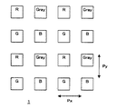
本発明の一実施の形態として固体撮像素子のカラーフィルタの色配列を図1に示す。
本実施の形態のカラーフィルタ1は、図11に示した原色系ベイヤー配列のカラーフィルタにおいて、レッドフィルタRに水平方向で隣接するグリーンフィルタGをグレイフィルタGrayに置き換えた場合である。
これにより、レッドR、グリーンG、ブルーB、グレイGrayの4色のフィルタが、水平方向・垂直方向ともに1画素おきに存在している。
【0018】
グレイフィルタは、他の3原色のフィルタと同様にして形成することが可能である。例えばグレイの染料(または顔料)を含有したレジスト等により形成することができる。
【0019】
また、グレイフィルタは、可視光線の分光領域で比較的波長依存性の少ないフラットな光学特性を有している。
そして、グレイフィルタも他の色のフィルタと同様に、例えば染料・顔料の含有量を変更することにより、フィルタの透過率を多くしたり少なくしたりして透過特性を変更することが可能である。
【0020】
グレイフィルタの透過特性は、上述のようにして変更可能であるが、機能的には次の3種類に大別される。
(1)透過率100%に近い理想的なホワイトに近い透過特性
(2)可視光分光領域における積分値がグリーンフィルタと同等な透過率を有する透過特性
(3)上記以外の透過率を有する透過特性
これらの場合のグレイフィルタの透過特性を、他の3原色のフィルタの透過特性と共に図2に示す。
【0021】
(1)透過率100%に近い理想ホワイト特性(図2のGray(1)の場合)この場合、RGB各色の感度と比較して、グレイ画素の感度は2倍以上と高い。これにより、S/N比の改善が可能となる。
また、後述するキャリアバランスをとると、グレイGray画素の出力をRGB各色の感度と同じようになるようにするので、負の利得をもつことになるが、これにより輝度信号や色差信号のS/N比を改善することができる。
【0022】
(2)可視光分光領域における積分値がグリーンフィルタと同等な透過率を有するグレイ分光(図2のGray(2)の場合)
(1)の場合、グレイフィルタが他のRGBフィルタに比較して感度が高いため、同一光量に対してグレイフィルタが他の色フィルタより早く飽和する。
従って、グレイフィルタGrayの可視光分光領域における積分値がグリーンフィルタGと同じようになるような透過率にすることで、ダイナミックレンジをRGBフィルタと同等にすることが可能である。
【0023】
(3)上記以外の透過率を有するグレイ分光(図2のGray(3)の場合)
グレイフィルタGrayの可視光分光領域における積分値をグリーンフィルタG以下となるような透過率にすることで、輝度のダイナミックレンジをRGBフィルタ以上の特性にすることが可能である。
ただし、この場合グレイフィルタGrayの感度はグリーンGよりも小さいので、感度もしくはS/N比の点では(1)(2)の場合よりも劣る。
【0024】
グレイフィルタGrayは、上述のようにフラットな透過特性を有するため、可視光領域の全ての色相の光に対して応答を持つ。
従って、RGB各画素の感度値と同等の信号出力となるようにそれぞれ利得を制御することにより、グレイフィルタGrayの画素の出力を信号処理におけるRGBそれぞれのフィルタ出力信号として代用可能である。
【0025】
まず、グリーンGのフィルタ出力信号について考える。図3Aにグリーン成分となるフィルタの配置を示す。図3Aにおいて、左下の元々のグリーンフィルタGreenに加えて、右上のグレイフィルタもグリーン成分Greenを構成する。図3Aではグレイフィルタは元々のグリーンフィルタと区別するため、斜線を付加して示している。
この場合、グリーン成分Greenとなる画素の配置は図11のベイヤー配列のグリーンGと同じであるので、グリーン成分Greenの空間周波数特性は、図3Bに示すように、先に示した図12Aの場合と等しくなる。
【0026】
次に、レッドRのフィルタ出力信号について考える。図4Aにレッド成分となるフィルタの配置を示す。図4Aにおいて、左上の元々のレッドフィルタRedに加えて、右上のグレイフィルタもレッド成分Redを構成する。図4Aではグレイフィルタは元々のレッドフィルタと区別するため、斜線を付加して示している。
この場合、レッド成分Redとなる画素は左上と右上即ち上半分である。従って、水平方向には毎画素存在し、垂直方向には1画素おきに存在する。これにより、レッド成分Redの空間周波数特性は、図4Bに示すように、水平空間周波数は図12Bの場合の2倍の1/2となり、その一方垂直空間周波数は図12Bの場合と同じ1/4となる。また、画素の個数は2倍となるので、図4Bの面積が図12Bの面積の2倍となっている。即ちレッドの情報量が2倍になっている。
【0027】
続いて、ブルーBのフィルタ出力信号について考える。図5Aにブルー成分となるフィルタの配置を示す。図5Aにおいて、右下の元々のブルーフィルタBlueに加えて、右上のグレイフィルタもブルー成分Blueを構成する。図5Aではグレイフィルタは元々のブルーフィルタと区別するため、斜線を付加して示している。
この場合、ブルー成分Blueとなる画素は右下と右上即ち右半分である。従って、水平方向には1画素おきに存在し、垂直方向には毎画素存在する。これにより、ブルー成分Blueの空間周波数特性は、図5Bに示すように、水平空間周波数は図12Cの場合と同じ1/4となり、その一方垂直空間周波数は図12Cの場合の2倍の1/2となる。また、画素の個数は2倍となるので、図5Bの面積が図12Cの面積の2倍となっている。即ちブルーの情報量が2倍になっている。
【0028】
つまり、図11に示す従来のベイヤー配列では、レッドRとブルーBの画素はグリーンGの画素に対して半分の情報量であったのが、本実施の形態ではグレイフィルタGrayを用いることにより従来の2倍の情報として扱えるため、レッドR・グリーンG・ブルーBの各画素の情報量を同等とすることができる。
即ち空間周波数特性として、レッドRとブルーBの通過帯域が従来の2倍になる。
【0029】
次に、レッド、グリーン、ブルー、グレイの4色のフィルタからアパコン信号(輪郭補正信号)を生成する方法について説明する。
図7に信号処理のブロック図を示す。この図7に示す信号処理は、4色の画素の出力信号(例えばCCD型固体撮像素子の場合はCCD出力)から、各種処理を行って、輝度信号Yと色差信号Cとを得るものである。
【0030】
(1)まず、グレイフィルタの画素の出力を、RGB各画素の感度値と同等の信号出力となるようにそれぞれ利得を制御する必要がある。これをキャリアバランスと言う。
ここで、図6に示すように、全画素を4色のフィルタを1つずつ含む2×2の4画素ずつの区画に区切って、この2×2の4画素の各色のフィルタを、それぞれRedij、Greenij、Blueij、Grayij(i,jは0以上の整数によるアドレス)とする。
【0031】
そして、この場合、以下の数式により、それぞれグリーン、レッド、ブルーに対してキャリアバランスがなされる。
(グリーンキャリアバランス)
Green(i,j)´=Gray(i,j)×〔Σ(グリーン出力値)〕/〔Σ(グレイ出力値)〕
ただし、Σの範囲は対象画素アドレス(i,j)に対して±N画素の領域
(レッドキャリアバランス)
Red(i,j)´=Gray(i,j)×〔Σ(レッド出力値)〕/〔Σ(グレイ出力値)〕
ただし、Σの範囲は対象画素アドレス(i,j)に対して±N画素の領域
(ブルーキャリアバランス)
Blue(i,j)´=Gray(i,j)×〔Σ(ブルー出力値)〕/〔Σ(グレイ出力値)〕
ただし、Σの範囲は対象画素アドレス(i,j)に対して±N画素の領域
【0032】
このようにキャリアバランスを行った出力Green(i,j)´,Red(i,j)´,Blue(i,j)´を、各色の出力として後段の回路に出力する。
【0033】
実際には、このキャリアバランスの処理は、図7に示すように通常の信号処理回路でも行われるホワイトバランス回路12の前段の回路11で行う。
【0034】
(2)次に、キャリアバランスの後のホワイトバランス補正処理を行う。
例えば白い被写体を撮像した場合、本来R,G,Bは同じレベルになるはずだが、R,G,B各色のフィルタの分光特性の違い(図2参照)により、必ずしも同一レベルとはならない。
このとき、R,G,Bのそれぞれに利得を持たせることにより、白を撮像したときにR=G=Bになるようにする。
これにより、各色毎の感度差を補正して、白い被写体は白く見えるようにする。
これをホワイトバランス補正と呼び、通常のグレイフィルタのない通常のカラーフィルタでも行われる処理である。
図7のブロック図では、ホワイトバランス回路12でホワイトバランス補正が行われ、出力WBoutを得る。
【0035】
(3)次に、各色の出力信号から輝度信号と色差信号とを生成するために、全画素に対して3倍のRGBデータを作り出す。
これを補間と呼ぶ。
即ち4色の出力信号である、R,Gray,R,Gray,・・・・,G,B,G,B・・・・のような点順次のデータからR,R,R,R,R,R,・・・・,G,G,G,G,G,G,・・・・,B,B,B,B,B,・・・・のような毎画素RGBが存在する3種類のRGBデータに変換する。これにより、例えば100画素からはR,G,Bを100ずつ含む300のデータを得る。
図7のブロック図では、ホワイトバランス回路12の出力WBoutから、Red補間回路13R、Green補間回路13G、Blue補間回路13Bで、各色の補間が行われる。
【0036】
(4)また、補間の処理と並行してアパコン信号(輪郭補正信号)を生成する。
このアパコン信号の生成は、ホワイトバランス補正の後、図7のアパコン合成回路14において行われる。図8に図7のアパコン合成回路14の構成を示す。
図8に示すように、アパコン合成回路14では、まずホワイトバランス出力の信号WBoutをRed/Gray、Green/Gray、及びBlue/Grayの3種類の信号系に分離する。これを色分離という。
【0037】
色分離を行った後、3種類の信号系それぞれでアパコン回路21R,21G,21Bを通す。
続いて、それぞれのアパコン回路21R,21G,21Bの出力信号に対して、増幅器22R,22G,22Bによってそれぞれレッド系がゲインα、グリーン系がゲインβ、ブルー系がゲインγの利得制御を行う。通常はα=β=γ=1である。
最後に3系統の信号を混合し、アパコン信号出力APoutとして出力する。
【0038】
さらに、各色のアパコン回路21R,21G,21Bの詳細な構成を図9に示す。上述の色分離がなされた後の信号を、図9の上下2系統で使用する。上側は垂直アパコン信号ap_vを生成する系統vであり、下側は水平アパコン信号ap_hを生成する系統hである。
垂直アパコン信号ap_vは、最初に水平方向のローパスフィルタ31をかけて、水平方向の演算ap_v(u)を行って高域信号をカットする。その後、垂直方向のバンドパスフィルタ32により、垂直方向の演算ap_v(v)を行って垂直高域信号を生成する。
水平アパコン信号ap_hは、最初に垂直方向のローパスフィルタ34をかけて、垂直方向の演算ap_h(v)を行って垂直の高域信号をカットする。その後、水平方向のバンドパスフィルタ35により、水平方向の演算ap_h(u)を行って水平高域信号を生成する。
尚、各方向の演算においては、ある特定画素の周囲の画素(前後或いは左右の数画素)の画素を使用して演算を行えばよい。これにより、例えばローパスフィルタ31,33ではその特定画素の信号をぼかして、バンドパスフィルタ32,34ではその特定画素の信号を強調して、アパコン信号(輪郭補正信号)の元とすることができる。
そして、垂直アパコン信号ap_vには増幅器33でゲインk、水平アパコン信号ap_hには増幅器36でゲインlをかけて、その後2系統の信号を混合し、各RGBアパコン信号として出力する。この出力に図8の増幅器22R,22G,22Bにおいて利得制御を行って3色のアパコン信号を合成することにより、アパコン信号出力APoutが得られる。
【0039】
(5)次に、補間処理した信号とアパコン信号を合成し、ガンマ補正を行う。
ここで、モニタ、ディスプレイに用いられるCRT(陰極線管)は、非線形な入出力特性を持っており、低輝度側の発光が入力に比例せず、小さく出る傾向がある。
従って、RGB信号を直接ディスプレイに表示した場合、低輝度側がつぶれたような、言い換えると暗く見える。これをCRTのガンマ特性と呼ぶ。
このとき、入力するRGB信号にガンマ特性と逆の特性を有する非線形処理をすることで、モニタ、ディスプレイで見たとき、自然なコントラストになる。これをガンマ補正と呼ぶ。
【0040】
ガンマ補正は、各補間回路13R,13G,13Bにより補間された信号とアパコン合成回路14の出力APoutとを合成した後、ガンマ補正回路15により行われる。
【0041】
(6)ガンマ補正を行ったR,G,B各色の信号を、それぞれ輝度信号合成回路16及び色差信号合成回路17に送り、輝度信号合成回路16で輝度信号Yを生成し、色差信号合成回路17で色差信号Cを生成する。
このようにして、輪郭補正処理がなされている輝度信号Y及び色差信号Cを得ることができる。
【0042】
上述の本実施の形態によれば、原色系ベイヤー配列のカラーフィルタにおいて、グリーンフィルタGreenの特定の画素をグレイフィルタGrayに置き換えたことにより、グレイフィルタGrayの画素では、全ての色相の光に対して透過する特性を有するので、R,G,B3色の信号を得ることができる。
これにより、グリーン成分が非常に少ない被写体、例えば赤や青の原色系の被写体に対しても輪郭強調を行うことができる。
従って、有彩色における解像度を改善することが可能となり、良好な画像を得ることができる。
【0043】
そして、比較的可視光分光領域でフラットな透過特性を持つグレイフィルタに置き換えたことにより、図2に示したGray(1),Gray(2),Gray(3)の3種類の透過率を選択することにより、感度の改善もしくは、ダイナミックレンジの改善効果を得ることができる。
【0044】
上述の実施の形態では、ベイヤー配列のカラーフィルタを具備した固体撮像素子に本発明を適用したが、本発明においてカラーフィルタの色配列はベイヤー配列には限定されず、その他の原色系(R,G,B)の色配列にも適用することができる。
【0045】
本発明を適用する他の色配列の例を図10A及び図10Bに示す。
図10Aは、いわゆるGストライプと呼ばれる色配列である。グリーンフィルタGを1列おきに縦一列に配置し、グリーンフィルタGの各列の間の列にレッドフィルタR及びブルーフィルタBを配置している。レッドフィルタR及びブルーフィルタBは市松配置となっている。
この色配列に本発明を適用する場合には、例えば図中*印を付したグリーンフィルタG、即ちレッドフィルタRの左隣のグリーンフィルタGをグレイフィルタに置き換えればよい。(或いは*印を付していないグリーンフィルタG、即ちレッドフィルタRの右隣のグリーンフィルタGをグレイフィルタに置き換えてもよい。)
これにより、前述のベイヤー配列に適用した実施の形態と同様に、グレイフィルタの画素においてR,G,B3色の信号の出力を得ることができ、色による解像感の偏りをなくす効果が得られる。
尚、Gストライプの色配列としては、レッドフィルタR及びブルーフィルタBの他の配置も考えられる。
【0046】
図10Bは、特にCCD固体撮像素子で垂直方向2画素を加算して出力する場合の色配列である。図11に示したベイヤー配列の各色R,G,Bの画素を垂直方向2画素に分割した形になっている。
この色配列に本発明を適用する場合には、例えば図中*印を付したグリーンフィルタG、即ちレッドフィルタRの水平隣のグリーンフィルタGをグレイフィルタに置き換えればよい。
これにより、図1の実施の形態と同様に、グレイフィルタの画素においてR,G,B3色の信号の出力を得ることができ、垂直2画素を加算して出力した信号を処理することにより、色による解像感の偏りをなくす効果が得られる。
【0047】
本発明は、CCD固体撮像素子にもMOS型の固体撮像素子にも適用することができ、いずれの固体撮像素子においても、同様に本発明を適用してグレイフィルタを有するオンチップカラーフィルタを形成することにより、色による解像感の偏りをなくして、良好な画像を得ることが可能である。
【0048】
尚、本発明におけるグレイフィルタを備えたカラーフィルタは、各種画像表示装置(ディスプレイ)にも使用可能であるが、特に固体撮像素子に使用した場合に、上述の色による解像感の偏りをなくして、良好な画像を得る効果を有するものである。
【0049】
本発明は、上述の実施の形態に限定されるものではなく、本発明の要旨を逸脱しない範囲でその他様々な構成が取り得る。
【0050】
【発明の効果】
上述の本発明によれば、原色系色配列のカラーフィルタにおいて、特定の画素をグレイフィルタに置き換えたことにより、グレイフィルタの画素では、原色の各色の信号を得ることができる。
これにより、色による解像感の偏りの発生をなくし、原色系の被写体でも輪郭強調をつけることができる。
従って、有彩色における解像度を改善することが可能となり、良好な画像を得ることができる。
【0051】
また本発明によれば、比較的可視光分光領域でフラットな透過特性を持つグレイフィルタを備えたことにより、グレイフィルタの透過率を選定することによって、感度の改善効果もしくは、ダイナミックレンジの改善効果を得ることができる。
【図面の簡単な説明】
【図1】本発明の一実施の形態の固体撮像素子のカラーフィルタの色配列を示す図である。
【図2】図1のカラーフィルタにおける各色のフィルタの分光特性を示す図である。
【図3】図1のカラーフィルタにおけるグリーン成分を示す図である。
A グリーン成分の配列を示す図である。
B グリーン成分の空間周波数特性を示す図である。
【図4】図1のカラーフィルタにおけるレッド成分を示す図である。
A レッド成分の配列を示す図である。
B レッド成分の空間周波数特性を示す図である。
【図5】図1のカラーフィルタにおけるブルー成分を示す図である。
A ブルー成分の配列を示す図である。
B ブルー成分の空間周波数特性を示す図である。
【図6】図1のカラーフィルタの各画素にアドレスを付した図である。
【図7】信号処理ブロックを示す図である。
【図8】図7のアパコン合成回路の構成を示す図である。
【図9】図8の各色のアパコン回路の詳細な構成を示す図である。
【図10】A、B 本発明を適用するカラーフィルタの色配列の他の例を示す図である。
【図11】ベイヤー配列を示す図である。
【図12】A〜C 図11のベイヤー配列における各色の空間周波数特性を示す図である。
【符号の説明】
1 カラーフィルタ、11 キャリアバランス回路、12 ホワイトバランス回路、14 アパコン合成回路、15 ガンマ補正回路、16 輝度信号合成回路、17 色差信号合成回路、21R,21G,21B アパコン回路、31 水平ローパスフィルタ、32 垂直バンドパスフィルタ、33 垂直ローパスフィルタ、34 水平バンドパスフィルタ[0001]
BACKGROUND OF THE INVENTION
The present invention relates to a single-plate type solid-state imaging device comprising a primary color filter. And signal processing method thereof Related to.
[0002]
[Prior art]
In a single-plate color solid-state imaging device, an on-chip color filter is formed on the sensor unit, and this on-chip color filter is configured by repeatedly arranging a plurality of color filters in a predetermined arrangement. The color signal is output.
[0003]
There are many types of color coding (color arrangement) of this color filter.
Among these, the so-called Bayer arrangement is adopted in the primary color system (three colors of red R, green G, and blue B).
[0004]
This Bayer arrangement is shown in FIG.
Looking at 4 pixels of 2 vertical pixels × 2 horizontal pixels, green (green) G is diagonally arranged in two diagonal positions, one of the remaining two locations is red (red) R, and the other is blue (blue) ) B is arranged.
Overall, green G is arranged in an oblique direction.
[0005]
The feature of this Bayer arrangement is that every pixel of green G contributing to resolution is seen only in the horizontal direction or only in the vertical direction. In the figure, Px represents the pixel pitch in the horizontal direction, and Py represents the pixel pitch in the vertical direction.
This has the following characteristics.
[0006]
(1) The spatial frequency characteristics in the horizontal direction and the vertical direction are isotropic.
FIG. 12 shows the spatial frequency characteristics of the three primary colors in the horizontal direction and the vertical direction in the Bayer arrangement of FIG. 12A shows green G, FIG. 12B shows red R, and FIG.
From FIG. 12B and FIG. 12C, red R and blue B exist every other pixel both in the horizontal direction and in the vertical direction. Thereby, the horizontal spatial frequency (1 / Px) and the vertical spatial frequency (1 / Py) are 1/4.
On the other hand, from FIG. 12A, as described above, the green G exists every pixel both in the horizontal direction and in the vertical direction, and the horizontal spatial frequency (1 / Px) and the vertical spatial frequency (1 / Py) are 1 / P. 2 and 2 times that of Red R and Blue B. However, since it exists every other pixel in the diagonal direction, it is the same as Red R and Blue B.
Accordingly, the horizontal spatial frequency and the vertical spatial frequency are the same for all three colors.
[0007]
(2) An aperture control signal (contour correction signal) having a relatively high resolution can be generated with only green G pixels.
Making an aperture control signal with only green G pixels has the advantage that it can be realized with relatively small hardware compared to a method for making an aperture control signal using all three colors of pixels. .
[0008]
[Problems to be solved by the invention]
However, in an RGB (primary color) Bayer array color filter, an aperture control signal is generated only from a signal from a green G pixel, so that a sense of resolution may be biased depending on the color. .
This is because when an aperture control signal is generated using only a green G signal, it is biased toward the green component due to spectral characteristics. Therefore, the aperture control is applied to a subject of a primary color system hue that does not include green G such as red R and blue B. It is difficult to generate a signal.
That is, for example, a red rose or the like is not easily emphasized even though the subject is highly saturated.
[0009]
In order to solve the above-described problems, in the present invention, a solid-state imaging device that eliminates the occurrence of bias in resolution due to color and provides a good image with edge enhancement. And signal processing method thereof Is to provide.
[0010]
[Means for Solving the Problems]
The solid-state imaging device of the present invention is a single-plate type solid-state imaging device comprising a primary color filter, and a specific pixel in an array of three primary color filters in the color filter. The integral value in the visible light spectral region has a transmittance equivalent to that of the green filter or a transmittance equal to or lower than that of the green filter. A gray filter is arranged and formed.
A signal processing method for a solid-state imaging device according to the present invention includes a primary color filter, and in the color filter, a specific pixel in an array of three primary color filters is provided. The integral value in the visible light spectral region has a transmittance equivalent to that of the green filter or a transmittance equal to or lower than that of the green filter. A single plate type solid-state imaging device having a gray filter arranged and formed, and having means for balancing the carrier so that the gray filter has frequency characteristics equivalent to the filters of the other three primary colors and means for synthesizing a contour correction signal On the other hand, the carrier balance processing is performed from the output signals of the four primary color filters and the gray color pixels, and the white balance processing is performed. Further, the interpolation is performed to form three times the data for all the pixels. Processing is performed to generate a contour correction signal in parallel with the interpolation processing, and the generated contour correction signal is combined with the interpolated signal.
[0011]
According to the above-described configuration of the solid-state imaging device of the present invention, the specific pixels of the filter array of the three primary colors (red, green, and blue) The integral value in the visible light spectral region has a transmittance equivalent to that of the green filter or a transmittance equal to or lower than that of the green filter. By arranging the gray filter, signals of the three primary colors (red, green, and blue) can be detected in the pixel in which the gray filter is arranged. Processing of output signals of primary colors (red, green, blue) can be performed.
According to the signal processing method of the solid-state imaging device of the present invention described above, the carrier balance processing is performed from the output signals of the four primary color filters and the gray color pixels, the white balance processing is performed, Three primary colors are generated by performing interpolation processing to form three times the data for the pixel, generating a contour correction signal in parallel with the interpolation processing, and synthesizing the generated contour correction signal with the interpolated signal. Processing of output signals of each color (red, green, blue) can be performed.
[0012]
DETAILED DESCRIPTION OF THE INVENTION
The present invention relates to a single-plate type solid-state imaging device comprising a primary color filter, and a specific pixel in an array of three primary color filters in the color filter. The integral value in the visible light spectral region has a transmittance equivalent to that of the green filter or a transmittance equal to or lower than that of the green filter. This is a solid-state imaging device in which a gray filter is arranged and formed.
[0013]
According to the present invention, in the solid-state imaging device, the color filter color array is a Bayer array, and the green filter horizontally adjacent to the red filter or the green filter horizontally adjacent to the blue filter is replaced with a gray filter. .
[0014]
The present invention A color filter of a primary color system, in which a specific pixel in the arrangement of the three primary color filters has a transmittance equal to that of the green filter or a transmittance equal to or lower than that of the green filter in the visible light spectral region. A single-plate solid-state imaging device comprising: a gray filter having an arrangement, and means for balancing a carrier so that the gray filter has frequency characteristics equivalent to those of other three primary color filters; and means for synthesizing a contour correction signal The element is subjected to carrier balance processing from the output signals of the four primary color filters and the gray color pixel, white balance processing, and three times as much data as all the pixels. Interpolation signal is generated in parallel with the interpolation process, and the generated contour correction signal is interpolated. A signal processing method for synthesizing to a solid-state imaging device.
In the signal processing method for a solid-state imaging device according to the present invention, the color arrangement of the color filters of the solid-state imaging device is a Bayer arrangement, and the green filter next to the red filter or the green filter next to the blue filter is gray. The configuration is replaced with a filter.
[0015]
In the present invention, a color filter is formed by replacing only a specific pixel with a gray filter in an array of primary color (red, green, blue) color filters.
[0016]
For example, in the case of the primary color Bayer array color filter shown in FIG. 11, the green G adjacent to the red R in the horizontal direction is replaced with gray, or the green G adjacent to the blue B in the horizontal direction is replaced with gray.
[0017]
As an embodiment of the present invention, the color arrangement of the color filter of the solid-state imaging device is shown in FIG.
The
Thereby, four color filters of red R, green G, blue B, and gray gray are present every other pixel in both the horizontal direction and the vertical direction.
[0018]
The gray filter can be formed in the same manner as the other three primary color filters. For example, it can be formed of a resist containing a gray dye (or pigment).
[0019]
Further, the gray filter has flat optical characteristics with relatively little wavelength dependence in the visible light spectral region.
As with other color filters, the gray filter can change the transmission characteristics by increasing or decreasing the transmittance of the filter, for example, by changing the dye / pigment content. .
[0020]
The transmission characteristics of the gray filter can be changed as described above, but are functionally classified into the following three types.
(1) Transmission characteristics close to ideal white, close to 100% transmittance
(2) Transmission characteristics in which the integrated value in the visible light spectral region has the same transmittance as that of the green filter
(3) Transmission characteristics having transmittances other than the above
The transmission characteristics of the gray filter in these cases are shown in FIG. 2 together with the transmission characteristics of the other three primary color filters.
[0021]
(1) Ideal white characteristics close to 100% transmittance (in the case of Gray (1) in FIG. 2) In this case, the sensitivity of gray pixels is as high as twice or more compared to the sensitivity of each RGB color. Thereby, the S / N ratio can be improved.
Further, when the carrier balance described later is taken, the output of the gray gray pixel is made to be the same as the sensitivity of each color of RGB, so that it has a negative gain. The N ratio can be improved.
[0022]
(2) Gray spectroscopy in which the integrated value in the visible light spectral region has the same transmittance as that of the green filter (in the case of Gray (2) in FIG. 2)
In the case of (1), since the gray filter has higher sensitivity than the other RGB filters, the gray filter saturates faster than the other color filters for the same amount of light.
Therefore, by setting the transmittance such that the integrated value of the gray filter Gray in the visible light spectral region is the same as that of the green filter G, the dynamic range can be made equivalent to that of the RGB filter.
[0023]
(3) Gray spectrum having transmittance other than the above (in the case of Gray (3) in FIG. 2)
By setting the integration value of the gray filter Gray in the visible light spectral region to a transmittance that is equal to or lower than that of the green filter G, it is possible to make the dynamic range of luminance higher than that of the RGB filter.
However, in this case, since the sensitivity of the gray filter Gray is smaller than that of the green G, the sensitivity or S / N ratio is inferior to the cases of (1) and (2).
[0024]
Since the gray filter Gray has a flat transmission characteristic as described above, it has a response to light of all hues in the visible light region.
Therefore, by controlling the gain so that the signal output is equivalent to the sensitivity value of each RGB pixel, the output of the pixel of the gray filter Gray can be substituted as the RGB filter output signal in the signal processing.
[0025]
First, consider the green G filter output signal. FIG. 3A shows the arrangement of filters that are green components. In FIG. 3A, in addition to the original green filter Green at the lower left, the upper right gray filter also constitutes the green component Green. In FIG. 3A, the gray filter is shown with diagonal lines to distinguish it from the original green filter.
In this case, since the arrangement of the pixels to be the green component Green is the same as that of the green G in the Bayer array in FIG. 11, the spatial frequency characteristics of the green component Green are as shown in FIG. Is equal to
[0026]
Next, consider the red R filter output signal. FIG. 4A shows the arrangement of filters that are red components. In FIG. 4A, in addition to the original red filter Red at the upper left, the upper right gray filter also constitutes the red component Red. In FIG. 4A, the gray filter is shown with hatching to distinguish it from the original red filter.
In this case, the pixels to be the red component Red are the upper left and upper right, that is, the upper half. Therefore, every pixel exists in the horizontal direction, and every other pixel exists in the vertical direction. As a result, as shown in FIG. 4B, the spatial frequency characteristic of the red component Red is ½ of the horizontal spatial frequency in the case of FIG. 12B, while the vertical spatial frequency is the same as in the case of FIG. 4. Further, since the number of pixels is doubled, the area of FIG. 4B is twice the area of FIG. 12B. That is, the information amount of red is doubled.
[0027]
Next, a blue B filter output signal will be considered. FIG. 5A shows the arrangement of filters that are blue components. In FIG. 5A, in addition to the original blue filter Blue at the lower right, the upper right gray filter also constitutes the blue component Blue. In FIG. 5A, the gray filter is shown with hatching to distinguish it from the original blue filter.
In this case, the pixels that become the blue component Blue are the lower right and upper right, that is, the right half. Therefore, every other pixel exists in the horizontal direction, and every pixel exists in the vertical direction. Accordingly, as shown in FIG. 5B, the spatial frequency characteristic of the blue component Blue is ¼ the horizontal spatial frequency as in FIG. 12C, while the vertical spatial frequency is 1 / twice that in FIG. 12C. 2 Further, since the number of pixels is doubled, the area of FIG. 5B is twice the area of FIG. 12C. That is, the amount of blue information is doubled.
[0028]
That is, in the conventional Bayer array shown in FIG. 11, the red R and blue B pixels have half the amount of information as compared to the green G pixels, but in the present embodiment, the gray filter Gray is used so far. Therefore, the information amount of each pixel of red R, green G, and blue B can be made equal.
That is, as a spatial frequency characteristic, the pass band of red R and blue B is twice that of the conventional one.
[0029]
Next, a method for generating an aperture control signal (contour correction signal) from four color filters of red, green, blue, and gray will be described.
FIG. 7 shows a block diagram of signal processing. The signal processing shown in FIG. 7 is to obtain a luminance signal Y and a color difference signal C by performing various processes from the output signals of pixels of four colors (for example, CCD output in the case of a CCD type solid-state imaging device). .
[0030]
(1) First, output the gray filter pixels. The sensitivity value of each pixel of RGB Equivalent Signal output To be Gain each Need to control. This is called career balance.
Here, as shown in FIG. 6, all pixels are divided into 2 × 2 4 pixel sections each including 4 color filters, and the 2 × 2 4 pixel color filters are respectively converted into Redij. , Greenij, Blueij, and Grayij (i and j are addresses based on integers of 0 or more).
[0031]
In this case, carrier balance is achieved for green, red, and blue, respectively, according to the following formulas.
(Green career balance)
Green (i, j) ′ = Gray (i, j) × [Σ (green output value)] / [Σ (gray output value)]
However, the range of Σ is an area of ± N pixels with respect to the target pixel address (i, j)
(Red carrier balance)
Red (i, j) ′ = Gray (i, j) × [Σ (red output value)] / [Σ (gray output value)]
However, the range of Σ is an area of ± N pixels with respect to the target pixel address (i, j)
(Blue carrier balance)
Blue (i, j) ′ = Gray (i, j) × [Σ (blue output value)] / [Σ (gray output value)]
However, the range of Σ is an area of ± N pixels with respect to the target pixel address (i, j)
[0032]
The outputs Green (i, j) ′, Red (i, j) ′, and Blue (i, j) ′ thus carrier-balanced are output to the subsequent circuit as outputs of each color.
[0033]
Actually, this carrier balance processing is performed by a circuit 11 in front of the
[0034]
(2) Next, white balance correction processing after carrier balance is performed.
For example, when a white subject is imaged, R, G, and B should originally be at the same level, but they are not necessarily at the same level due to the difference in spectral characteristics of the R, G, and B filters (see FIG. 2).
At this time, each of R, G, and B is given a gain so that R = G = B when white is imaged.
Thus, the sensitivity difference for each color is corrected so that a white subject appears white.
This is called white balance correction, and is a process performed by a normal color filter without a normal gray filter.
In the block diagram of FIG. 7, white balance correction is performed by the
[0035]
(3) Next, in order to generate a luminance signal and a color difference signal from the output signals of each color, RGB data that is three times as large as all pixels is created.
This is called interpolation.
That is, R, R, R, R, R from the dot sequential data such as R, Gray, R, Gray,..., G, B, G, B,. , R,..., G, G, G, G, G, G,..., B, B, B, B, B,. To RGB data. Thus, for example, 300 data including 100 R, G, and B are obtained from 100 pixels.
In the block diagram of FIG. 7, each color is interpolated from the output WBout of the
[0036]
(4) In addition, an aperture control signal (contour correction signal) is generated in parallel with the interpolation process.
The generation of the aperture control signal is performed by the aperture
As shown in FIG. 8, the
[0037]
After the color separation, the
Subsequently, with respect to the output signals of the respective
Finally, the signals of the three systems are mixed and output as aperture control signal output APout.
[0038]
Further, FIG. 9 shows a detailed configuration of the
The vertical aperture control signal ap_v is first subjected to a horizontal low-
The horizontal aperture control signal ap_h is first subjected to a vertical low-
In the calculation in each direction, the calculation may be performed using pixels of pixels around a specific pixel (front and rear or several pixels on the left and right). Thereby, for example, the signal of the specific pixel can be blurred by the low-
Then, the
[0039]
(5) Next, the interpolated signal and the aperture control signal are synthesized and gamma correction is performed.
Here, CRTs (cathode ray tubes) used for monitors and displays have nonlinear input / output characteristics, and light emission on the low luminance side tends not to be proportional to the input, but tends to be small.
Therefore, when the RGB signal is directly displayed on the display, it looks dark, in other words, the low luminance side is crushed. This is called the CRT gamma characteristic.
At this time, the input RGB signal is subjected to nonlinear processing having a characteristic opposite to the gamma characteristic, so that a natural contrast is obtained when viewed on a monitor or a display. This is called gamma correction.
[0040]
The gamma correction is performed by the
[0041]
(6) The R, G, B color signals subjected to gamma correction are sent to the luminance
In this way, the luminance signal Y and the color difference signal C that have been subjected to the contour correction process can be obtained.
[0042]
According to the above-described embodiment, by replacing specific pixels of the green filter Green with the gray filter Gray in the color filters of the primary color Bayer arrangement, the pixels of the gray filter Gray Therefore, R, G, B3 color signals can be obtained.
As a result, contour enhancement can be performed on a subject with very little green component, for example, a subject of primary colors of red and blue.
Therefore, the resolution in chromatic colors can be improved, and a good image can be obtained.
[0043]
Then, by replacing with a gray filter having a flat transmission characteristic in a relatively visible light spectral region, three types of transmittances of Gray (1), Gray (2), and Gray (3) shown in FIG. 2 are selected. By doing so, it is possible to obtain the effect of improving the sensitivity or the dynamic range.
[0044]
In the above-described embodiment, the present invention is applied to a solid-state imaging device having a Bayer array color filter. However, in the present invention, the color filter color array is not limited to the Bayer array, and other primary color systems (R, R, The present invention can also be applied to the color arrangement of G, B).
[0045]
Examples of other color arrangements to which the present invention is applied are shown in FIGS. 10A and 10B.
FIG. 10A shows a color arrangement called a so-called G stripe. Green filters G are arranged in a vertical row every other row, and red filters R and blue filters B are arranged in rows between the green filters G. The red filter R and the blue filter B are in a checkered arrangement.
When the present invention is applied to this color arrangement, for example, the green filter G marked with * in the figure, that is, the green filter G adjacent to the left of the red filter R may be replaced with a gray filter. (Alternatively, the green filter G not marked with *, that is, the green filter G on the right side of the red filter R may be replaced with a gray filter.)
As a result, similar to the embodiment applied to the Bayer arrangement described above, it is possible to obtain R, G, and B3 color signal outputs in the gray filter pixels, and the effect of eliminating the bias in resolution due to colors is obtained. It is done.
Note that other arrangements of the red filter R and the blue filter B are also conceivable as the color arrangement of the G stripe.
[0046]
FIG. 10B shows a color arrangement particularly in the case of adding and outputting two pixels in the vertical direction with a CCD solid-state imaging device. The pixels of each color R, G, B in the Bayer array shown in FIG. 11 are divided into two pixels in the vertical direction.
When the present invention is applied to this color arrangement, for example, the green filter G marked with * in the figure, that is, the green filter G horizontally adjacent to the red filter R may be replaced with a gray filter.
Thus, as in the embodiment of FIG. 1, it is possible to obtain the output of R, G, B3 color signals in the gray filter pixels, and by processing the output signal by adding the two vertical pixels, The effect of eliminating the bias in resolution due to color can be obtained.
[0047]
The present invention can be applied to both a CCD solid-state image pickup device and a MOS type solid-state image pickup device. In any solid-state image pickup device, the present invention is similarly applied to form an on-chip color filter having a gray filter. By doing so, it is possible to eliminate a bias in resolution due to colors and obtain a good image.
[0048]
The color filter provided with the gray filter according to the present invention can be used for various image display devices (displays), but particularly when used for a solid-state imaging device, the above-described bias in resolution is eliminated. Thus, it has an effect of obtaining a good image.
[0049]
The present invention is not limited to the above-described embodiment, and various other configurations can be taken without departing from the gist of the present invention.
[0050]
【The invention's effect】
According to the present invention described above, in the color filter of the primary color array, a specific pixel is replaced with a gray filter, so that a signal of each primary color can be obtained from the gray filter pixel.
As a result, it is possible to eliminate the occurrence of a bias in resolution due to colors, and to enhance the contour even in a primary color subject.
Therefore, the resolution in chromatic colors can be improved, and a good image can be obtained.
[0051]
Further, according to the present invention, by providing a gray filter having a flat transmission characteristic in a relatively visible light spectral region, by selecting the transmittance of the gray filter, it is possible to improve the sensitivity or the dynamic range. Can be obtained.
[Brief description of the drawings]
FIG. 1 is a diagram showing a color arrangement of a color filter of a solid-state image sensor according to an embodiment of the present invention.
FIG. 2 is a diagram showing spectral characteristics of filters of respective colors in the color filter of FIG.
FIG. 3 is a diagram illustrating a green component in the color filter of FIG.
It is a figure which shows the arrangement | sequence of A green component.
It is a figure which shows the spatial frequency characteristic of B green component.
FIG. 4 is a diagram illustrating a red component in the color filter of FIG.
It is a figure which shows the arrangement | sequence of A red component.
It is a figure which shows the spatial frequency characteristic of B red component.
FIG. 5 is a diagram illustrating a blue component in the color filter of FIG. 1;
It is a figure which shows the arrangement | sequence of A blue component.
It is a figure which shows the spatial frequency characteristic of B blue component.
6 is a diagram in which an address is assigned to each pixel of the color filter in FIG. 1. FIG.
FIG. 7 is a diagram illustrating a signal processing block.
8 is a diagram showing a configuration of the aperture control composition circuit of FIG. 7; FIG.
9 is a diagram showing a detailed configuration of each color aperture control circuit in FIG. 8;
FIGS. 10A and 10B are diagrams showing another example of a color arrangement of a color filter to which the present invention is applied.
FIG. 11 is a diagram illustrating a Bayer array.
FIGS. 12A to 12C are diagrams illustrating the spatial frequency characteristics of the respective colors in the Bayer array of FIG.
[Explanation of symbols]
DESCRIPTION OF
Claims (4)
上記カラーフィルタにおいて、3原色のフィルタの配列の特定の画素に、可視光分光領域における積分値がグリーンフィルタと同等な透過率、もしくはグリーンフィルタ以下の透過率を有するグレイフィルタが配置形成された
固体撮像素子。A single-plate solid-state image sensor comprising a primary color filter,
In the color filter described above, a gray filter having an integral value in the visible light spectral region equivalent to that of the green filter or a transmittance equal to or lower than that of the green filter is arranged and formed on a specific pixel in the arrangement of the three primary color filters. Image sensor.
上記カラーフィルタにおいて、3原色のフィルタの配列の特定の画素に、可視光分光領域における積分値がグリーンフィルタと同等な透過率、もしくはグリーンフィルタ以下の透過率を有するグレイフィルタが配置形成され、
上記グレイフィルタを、他の3原色のフィルタと同等の周波数特性となるようにキャリアバランスをとる手段と、
輪郭補正信号を合成する手段とを備えた単板式の固体撮像素子に対して、
3原色のフィルタ及びグレイフィルタの4色の画素の出力信号から、上記キャリアバランスをとる処理を行い、
ホワイトバランス処理を行い、
さらに、全画素に対して3倍のデータを形成する補間の処理を行い、
上記補間の処理と並行して、上記輪郭補正信号を生成して、
生成した上記輪郭補正信号を、補間処理した信号に合成する
固体撮像素子の信号処理方法。Comprising a primary color filter,
In the color filter, a gray filter having an integral value in the visible light spectral region equivalent to that of the green filter or a transmittance equal to or lower than that of the green filter is arranged and formed on a specific pixel in the arrangement of the three primary color filters.
Means for balancing the gray filter so as to have a frequency characteristic equivalent to the filters of the other three primary colors;
For a single-plate solid-state imaging device having a means for synthesizing a contour correction signal,
From the output signals of the three primary color filters and the four color pixels of the gray filter, the above carrier balance processing is performed,
Perform white balance processing,
Furthermore, an interpolation process is performed to form three times the data for all pixels,
In parallel with the interpolation process, the contour correction signal is generated,
A signal processing method for a solid-state imaging device, wherein the generated contour correction signal is combined with an interpolated signal.
Priority Applications (4)
| Application Number | Priority Date | Filing Date | Title |
|---|---|---|---|
| JP2000318081A JP4517493B2 (en) | 2000-10-18 | 2000-10-18 | Solid-state imaging device and signal processing method thereof |
| US09/982,304 US7126633B2 (en) | 2000-10-18 | 2001-10-17 | Solid-state image-pickup device having primary color and gray color filters and processing means thereof |
| US11/582,224 US7852389B2 (en) | 2000-10-18 | 2006-10-16 | Solid-state image pick-up device having primary color and gray color filters and processing means therefor |
| US12/966,655 US8848074B2 (en) | 2000-10-18 | 2010-12-13 | Solid-state image pickup device |
Applications Claiming Priority (1)
| Application Number | Priority Date | Filing Date | Title |
|---|---|---|---|
| JP2000318081A JP4517493B2 (en) | 2000-10-18 | 2000-10-18 | Solid-state imaging device and signal processing method thereof |
Publications (3)
| Publication Number | Publication Date |
|---|---|
| JP2002135792A JP2002135792A (en) | 2002-05-10 |
| JP2002135792A5 JP2002135792A5 (en) | 2007-04-12 |
| JP4517493B2 true JP4517493B2 (en) | 2010-08-04 |
Family
ID=18796763
Family Applications (1)
| Application Number | Title | Priority Date | Filing Date |
|---|---|---|---|
| JP2000318081A Expired - Lifetime JP4517493B2 (en) | 2000-10-18 | 2000-10-18 | Solid-state imaging device and signal processing method thereof |
Country Status (2)
| Country | Link |
|---|---|
| US (3) | US7126633B2 (en) |
| JP (1) | JP4517493B2 (en) |
Families Citing this family (39)
| Publication number | Priority date | Publication date | Assignee | Title |
|---|---|---|---|---|
| JP4517493B2 (en) * | 2000-10-18 | 2010-08-04 | ソニー株式会社 | Solid-state imaging device and signal processing method thereof |
| KR101081000B1 (en) * | 2003-10-23 | 2011-11-09 | 소니 가부시키가이샤 | Image processing apparatus and image processing method, and recording medium |
| EP1594321A3 (en) * | 2004-05-07 | 2006-01-25 | Dialog Semiconductor GmbH | Extended dynamic range in color imagers |
| DE502005003754D1 (en) | 2004-05-25 | 2008-05-29 | Vdo Automotive Ag | MONITORING UNIT NEBST ASSISTANCE SYSTEM FOR MOTOR VEHICLES |
| US7880785B2 (en) | 2004-07-21 | 2011-02-01 | Aptina Imaging Corporation | Rod and cone response sensor |
| BE1016426A3 (en) * | 2005-01-25 | 2006-10-03 | Ceulemans Jean Paul Jeanne | Device for increasing the dynamic range of digital capture systems. |
| EP1856652B1 (en) | 2005-03-11 | 2016-08-10 | Hand Held Products, Inc. | Digital picture taking optical reader having hybrid monochrome and color image sensor array |
| JP4984634B2 (en) | 2005-07-21 | 2012-07-25 | ソニー株式会社 | Physical information acquisition method and physical information acquisition device |
| JP5017812B2 (en) * | 2005-07-21 | 2012-09-05 | 凸版印刷株式会社 | Solid-state image sensor |
| US7830430B2 (en) * | 2005-07-28 | 2010-11-09 | Eastman Kodak Company | Interpolation of panchromatic and color pixels |
| US8139130B2 (en) | 2005-07-28 | 2012-03-20 | Omnivision Technologies, Inc. | Image sensor with improved light sensitivity |
| US8274715B2 (en) | 2005-07-28 | 2012-09-25 | Omnivision Technologies, Inc. | Processing color and panchromatic pixels |
| US7821553B2 (en) * | 2005-12-30 | 2010-10-26 | International Business Machines Corporation | Pixel array, imaging sensor including the pixel array and digital camera including the imaging sensor |
| JP4241840B2 (en) * | 2006-02-23 | 2009-03-18 | 富士フイルム株式会社 | Imaging device |
| JP4449936B2 (en) | 2006-03-31 | 2010-04-14 | ソニー株式会社 | Imaging apparatus, camera system, and driving method thereof |
| JP4967432B2 (en) * | 2006-04-14 | 2012-07-04 | ソニー株式会社 | Imaging apparatus and camera system |
| JP4187004B2 (en) * | 2006-04-17 | 2008-11-26 | ソニー株式会社 | Imaging apparatus and exposure control method for imaging apparatus |
| JP4867448B2 (en) * | 2006-04-18 | 2012-02-01 | ソニー株式会社 | Physical information acquisition method and physical information acquisition device |
| US7916362B2 (en) * | 2006-05-22 | 2011-03-29 | Eastman Kodak Company | Image sensor with improved light sensitivity |
| JP5106870B2 (en) * | 2006-06-14 | 2012-12-26 | 株式会社東芝 | Solid-state image sensor |
| KR100871564B1 (en) | 2006-06-19 | 2008-12-02 | 삼성전기주식회사 | Camera module |
| KR100772910B1 (en) * | 2006-06-26 | 2007-11-05 | 삼성전기주식회사 | Digital camera module |
| US8031258B2 (en) | 2006-10-04 | 2011-10-04 | Omnivision Technologies, Inc. | Providing multiple video signals from single sensor |
| JP4930109B2 (en) * | 2007-03-06 | 2012-05-16 | ソニー株式会社 | Solid-state imaging device, imaging device |
| KR100976284B1 (en) | 2007-06-07 | 2010-08-16 | 가부시끼가이샤 도시바 | Image pickup device |
| US8452082B2 (en) * | 2007-09-27 | 2013-05-28 | Eastman Kodak Company | Pattern conversion for interpolation |
| JP5262180B2 (en) | 2008-02-26 | 2013-08-14 | ソニー株式会社 | Solid-state imaging device and camera |
| KR101639382B1 (en) | 2008-08-27 | 2016-07-13 | 삼성전자주식회사 | Apparatus and method for generating HDR image |
| JP5375359B2 (en) * | 2009-06-22 | 2013-12-25 | ソニー株式会社 | Imaging device, charge readout method, and imaging apparatus |
| US8619143B2 (en) * | 2010-03-19 | 2013-12-31 | Pixim, Inc. | Image sensor including color and infrared pixels |
| JP5675215B2 (en) | 2010-08-20 | 2015-02-25 | オリンパス株式会社 | Digital camera |
| JP5757711B2 (en) * | 2010-09-27 | 2015-07-29 | オリンパス株式会社 | Spectral information measurement method, color sensor, and virtual slide device |
| JPWO2013089036A1 (en) | 2011-12-16 | 2015-04-27 | ソニー株式会社 | Imaging device |
| TWI552594B (en) | 2014-10-27 | 2016-10-01 | 聯詠科技股份有限公司 | Color filter array for image sensing device and manufacturing method thereof |
| CN105635699B (en) * | 2014-11-06 | 2019-10-18 | 联咏科技股份有限公司 | Color filter array and its manufacturing method for image sensing device |
| US11181671B2 (en) * | 2016-09-29 | 2021-11-23 | Nikon Corporation | Image sensor and electronic camera |
| JP6730916B2 (en) * | 2016-11-30 | 2020-07-29 | 日本放送協会 | Contrast correction device and program |
| US11172142B2 (en) * | 2018-09-25 | 2021-11-09 | Taiwan Semiconductor Manufacturing Co., Ltd. | Image sensor for sensing LED light with reduced flickering |
| CN112997478B (en) * | 2018-12-11 | 2024-03-19 | 索尼半导体解决方案公司 | Solid-state image pickup device and electronic apparatus |
Citations (1)
| Publication number | Priority date | Publication date | Assignee | Title |
|---|---|---|---|---|
| WO2000057651A1 (en) * | 1999-03-22 | 2000-09-28 | Biomorphic Vlsi, Inc. | Color image pickup apparatus |
Family Cites Families (20)
| Publication number | Priority date | Publication date | Assignee | Title |
|---|---|---|---|---|
| US3971065A (en) * | 1975-03-05 | 1976-07-20 | Eastman Kodak Company | Color imaging array |
| US4290671A (en) * | 1980-02-19 | 1981-09-22 | Rca Corporation | Color encoding filter |
| JPS57102281U (en) * | 1980-12-16 | 1982-06-23 | ||
| US4500914A (en) * | 1981-08-01 | 1985-02-19 | Sharp Kabushiki Kaisha | Color imaging array and color imaging device |
| JPS5875393A (en) * | 1981-10-29 | 1983-05-07 | Sharp Corp | Single plate type color image pickup device |
| DE69303545T2 (en) * | 1992-05-13 | 1996-10-31 | Matsushita Electric Ind Co Ltd | Solid state imaging device with a color filter matrix |
| JPH0823543A (en) * | 1994-07-07 | 1996-01-23 | Canon Inc | Image pickup device |
| JPH08116913A (en) | 1994-10-18 | 1996-05-14 | Kyodo Kumiai Shisupetsukusu | Production of fermented seasoning from fish as raw material |
| US5574816A (en) * | 1995-01-24 | 1996-11-12 | Alcatel Na Cable Sytems, Inc. | Polypropylene-polyethylene copolymer buffer tubes for optical fiber cables and method for making the same |
| US5768511A (en) * | 1995-09-18 | 1998-06-16 | International Business Machines Corporation | Method and system for managing objects in networked computer system with action performed in the server and object updated in the client |
| JP3820608B2 (en) * | 1995-10-23 | 2006-09-13 | 日本ビクター株式会社 | Video signal processing circuit |
| US6400403B1 (en) * | 1996-07-03 | 2002-06-04 | Sony Corporation | Solid-state imaging device having improved resolution without generating a pseudo signal |
| JPH1126737A (en) * | 1997-06-30 | 1999-01-29 | Victor Co Of Japan Ltd | Solid-state image sensing device |
| GB2345217A (en) * | 1998-12-23 | 2000-06-28 | Nokia Mobile Phones Ltd | Colour video image sensor |
| JP3913388B2 (en) * | 1999-02-01 | 2007-05-09 | 三洋電機株式会社 | Solid-state imaging device |
| GB2351866A (en) * | 1999-07-07 | 2001-01-10 | Sharp Kk | Stereoscopic display |
| US6900838B1 (en) * | 1999-10-14 | 2005-05-31 | Hitachi Denshi Kabushiki Kaisha | Method of processing image signal from solid-state imaging device, image signal processing apparatus, image signal generating apparatus and computer program product for image signal processing method |
| JP4517493B2 (en) * | 2000-10-18 | 2010-08-04 | ソニー株式会社 | Solid-state imaging device and signal processing method thereof |
| US6960753B2 (en) * | 2001-01-24 | 2005-11-01 | Hewlett-Packard Development Company, L.P. | Photosensor arrays with encoded permanent information |
| US20040105021A1 (en) * | 2002-12-02 | 2004-06-03 | Bolymedia Holdings Co., Ltd. | Color filter patterns for image sensors |
-
2000
- 2000-10-18 JP JP2000318081A patent/JP4517493B2/en not_active Expired - Lifetime
-
2001
- 2001-10-17 US US09/982,304 patent/US7126633B2/en not_active Expired - Lifetime
-
2006
- 2006-10-16 US US11/582,224 patent/US7852389B2/en not_active Expired - Lifetime
-
2010
- 2010-12-13 US US12/966,655 patent/US8848074B2/en not_active Expired - Lifetime
Patent Citations (1)
| Publication number | Priority date | Publication date | Assignee | Title |
|---|---|---|---|---|
| WO2000057651A1 (en) * | 1999-03-22 | 2000-09-28 | Biomorphic Vlsi, Inc. | Color image pickup apparatus |
Also Published As
| Publication number | Publication date |
|---|---|
| US7126633B2 (en) | 2006-10-24 |
| US8848074B2 (en) | 2014-09-30 |
| JP2002135792A (en) | 2002-05-10 |
| US20020044209A1 (en) | 2002-04-18 |
| US20110149127A1 (en) | 2011-06-23 |
| US20070035645A1 (en) | 2007-02-15 |
| US7852389B2 (en) | 2010-12-14 |
Similar Documents
| Publication | Publication Date | Title |
|---|---|---|
| JP4517493B2 (en) | Solid-state imaging device and signal processing method thereof | |
| US7414630B2 (en) | Hexagonal color pixel structure with white pixels | |
| JP3988457B2 (en) | Imaging apparatus and signal processing method for solid-state imaging device | |
| US9160935B2 (en) | Sensor arrangement for transforming color space representation in a digital color image | |
| US7847842B2 (en) | Preventing green non-uniformity in image sensors | |
| US6226034B1 (en) | Spatial non-uniformity correction of a color sensor | |
| US7072509B2 (en) | Electronic image color plane reconstruction | |
| US20030016295A1 (en) | Image signal processor | |
| JP4451044B2 (en) | Hybrid pixel interpolation device and hybrid pixel interpolation method | |
| US7305141B2 (en) | Contour filter for image sensor output signals | |
| US6747698B2 (en) | Image interpolating device | |
| JP2000316169A (en) | Color image pickup element and device | |
| JP2002010286A (en) | Signal processing apparatus, signal processing method and imaging apparatus | |
| JP2004056640A (en) | Interpolation method of photographed images in complementary color single ccd color digital camera, interpolation unit of the same, and digital camera comprising the same | |
| US20230269352A1 (en) | Solid-state imaging element, camera module, image processing device, and imaging method | |
| JP4119565B2 (en) | Color imaging device and color imaging device | |
| JP2001218099A (en) | Multiplate type image pickup device and recording medium for image data processing | |
| JP2000253413A (en) | Image pickup element and image pickup device | |
| GB2466375A (en) | Improved method for interpolation of tristimulus values on pixels of an image sensor. | |
| JPS58179083A (en) | Color solid state image pickup device | |
| KR20050014916A (en) | Method and apparatus for signal processing, computer program product, computing system and camera | |
| JPS6123488A (en) | Color solid-state image pickup device | |
| JPH04298191A (en) | Luminance signal synthesis circuit | |
| JPH0149076B2 (en) |
Legal Events
| Date | Code | Title | Description |
|---|---|---|---|
| A521 | Request for written amendment filed |
Free format text: JAPANESE INTERMEDIATE CODE: A523 Effective date: 20070226 |
|
| A621 | Written request for application examination |
Free format text: JAPANESE INTERMEDIATE CODE: A621 Effective date: 20070226 |
|
| A977 | Report on retrieval |
Free format text: JAPANESE INTERMEDIATE CODE: A971007 Effective date: 20090423 |
|
| A131 | Notification of reasons for refusal |
Free format text: JAPANESE INTERMEDIATE CODE: A131 Effective date: 20090512 |
|
| A521 | Request for written amendment filed |
Free format text: JAPANESE INTERMEDIATE CODE: A523 Effective date: 20090709 |
|
| A131 | Notification of reasons for refusal |
Free format text: JAPANESE INTERMEDIATE CODE: A131 Effective date: 20100302 |
|
| A521 | Request for written amendment filed |
Free format text: JAPANESE INTERMEDIATE CODE: A523 Effective date: 20100402 |
|
| TRDD | Decision of grant or rejection written | ||
| A01 | Written decision to grant a patent or to grant a registration (utility model) |
Free format text: JAPANESE INTERMEDIATE CODE: A01 Effective date: 20100427 |
|
| A01 | Written decision to grant a patent or to grant a registration (utility model) |
Free format text: JAPANESE INTERMEDIATE CODE: A01 |
|
| A61 | First payment of annual fees (during grant procedure) |
Free format text: JAPANESE INTERMEDIATE CODE: A61 Effective date: 20100510 |
|
| FPAY | Renewal fee payment (event date is renewal date of database) |
Free format text: PAYMENT UNTIL: 20130528 Year of fee payment: 3 |
|
| R151 | Written notification of patent or utility model registration |
Ref document number: 4517493 Country of ref document: JP Free format text: JAPANESE INTERMEDIATE CODE: R151 |
|
| R250 | Receipt of annual fees |
Free format text: JAPANESE INTERMEDIATE CODE: R250 |
|
| R250 | Receipt of annual fees |
Free format text: JAPANESE INTERMEDIATE CODE: R250 |
|
| R250 | Receipt of annual fees |
Free format text: JAPANESE INTERMEDIATE CODE: R250 |
|
| R250 | Receipt of annual fees |
Free format text: JAPANESE INTERMEDIATE CODE: R250 |
|
| R250 | Receipt of annual fees |
Free format text: JAPANESE INTERMEDIATE CODE: R250 |
|
| R250 | Receipt of annual fees |
Free format text: JAPANESE INTERMEDIATE CODE: R250 |
|
| R250 | Receipt of annual fees |
Free format text: JAPANESE INTERMEDIATE CODE: R250 |
|
| R250 | Receipt of annual fees |
Free format text: JAPANESE INTERMEDIATE CODE: R250 |