EP1908302B1 - Image sensor with improved lightsensitivity - Google Patents
Image sensor with improved lightsensitivity Download PDFInfo
- Publication number
- EP1908302B1 EP1908302B1 EP06800074.4A EP06800074A EP1908302B1 EP 1908302 B1 EP1908302 B1 EP 1908302B1 EP 06800074 A EP06800074 A EP 06800074A EP 1908302 B1 EP1908302 B1 EP 1908302B1
- Authority
- EP
- European Patent Office
- Prior art keywords
- pixels
- color
- image
- repeating unit
- cell
- Prior art date
- Legal status (The legal status is an assumption and is not a legal conclusion. Google has not performed a legal analysis and makes no representation as to the accuracy of the status listed.)
- Active
Links
Images


Classifications
-
- H—ELECTRICITY
- H04—ELECTRIC COMMUNICATION TECHNIQUE
- H04N—PICTORIAL COMMUNICATION, e.g. TELEVISION
- H04N23/00—Cameras or camera modules comprising electronic image sensors; Control thereof
- H04N23/80—Camera processing pipelines; Components thereof
- H04N23/84—Camera processing pipelines; Components thereof for processing colour signals
- H04N23/843—Demosaicing, e.g. interpolating colour pixel values
-
- H—ELECTRICITY
- H04—ELECTRIC COMMUNICATION TECHNIQUE
- H04N—PICTORIAL COMMUNICATION, e.g. TELEVISION
- H04N25/00—Circuitry of solid-state image sensors [SSIS]; Control thereof
- H04N25/10—Circuitry of solid-state image sensors [SSIS]; Control thereof for transforming different wavelengths into image signals
- H04N25/11—Arrangement of colour filter arrays [CFA]; Filter mosaics
- H04N25/13—Arrangement of colour filter arrays [CFA]; Filter mosaics characterised by the spectral characteristics of the filter elements
- H04N25/133—Arrangement of colour filter arrays [CFA]; Filter mosaics characterised by the spectral characteristics of the filter elements including elements passing panchromatic light, e.g. filters passing white light
-
- H—ELECTRICITY
- H04—ELECTRIC COMMUNICATION TECHNIQUE
- H04N—PICTORIAL COMMUNICATION, e.g. TELEVISION
- H04N25/00—Circuitry of solid-state image sensors [SSIS]; Control thereof
- H04N25/10—Circuitry of solid-state image sensors [SSIS]; Control thereof for transforming different wavelengths into image signals
- H04N25/11—Arrangement of colour filter arrays [CFA]; Filter mosaics
- H04N25/13—Arrangement of colour filter arrays [CFA]; Filter mosaics characterised by the spectral characteristics of the filter elements
- H04N25/134—Arrangement of colour filter arrays [CFA]; Filter mosaics characterised by the spectral characteristics of the filter elements based on three different wavelength filter elements
-
- H—ELECTRICITY
- H04—ELECTRIC COMMUNICATION TECHNIQUE
- H04N—PICTORIAL COMMUNICATION, e.g. TELEVISION
- H04N25/00—Circuitry of solid-state image sensors [SSIS]; Control thereof
- H04N25/10—Circuitry of solid-state image sensors [SSIS]; Control thereof for transforming different wavelengths into image signals
- H04N25/11—Arrangement of colour filter arrays [CFA]; Filter mosaics
- H04N25/13—Arrangement of colour filter arrays [CFA]; Filter mosaics characterised by the spectral characteristics of the filter elements
- H04N25/135—Arrangement of colour filter arrays [CFA]; Filter mosaics characterised by the spectral characteristics of the filter elements based on four or more different wavelength filter elements
- H04N25/136—Arrangement of colour filter arrays [CFA]; Filter mosaics characterised by the spectral characteristics of the filter elements based on four or more different wavelength filter elements using complementary colours
-
- H—ELECTRICITY
- H04—ELECTRIC COMMUNICATION TECHNIQUE
- H04N—PICTORIAL COMMUNICATION, e.g. TELEVISION
- H04N23/00—Cameras or camera modules comprising electronic image sensors; Control thereof
- H04N23/60—Control of cameras or camera modules
- H04N23/63—Control of cameras or camera modules by using electronic viewfinders
- H04N23/633—Control of cameras or camera modules by using electronic viewfinders for displaying additional information relating to control or operation of the camera
Definitions
- This invention relates to a two-dimensional image sensor with improved light sensitivity
- An electronic imaging system depends on an electronic image sensor to create an electronic representation of a visual image.
- electronic image sensors include charge coupled device (CCD) image sensors and active pixel sensor (APS) devices (APS devices are often referred to as CMOS sensors because of the ability to fabricate them in a Complementary Metal Oxide Semiconductor process).
- CCD charge coupled device
- APS active pixel sensor
- CMOS sensors because of the ability to fabricate them in a Complementary Metal Oxide Semiconductor process.
- CMOS sensors active pixel sensor
- CMOS sensors active pixel sensor
- CMOS sensors active pixel sensor
- CMOS sensors active pixel sensor
- CMOS sensors active pixel sensor
- CMOS sensors active pixel sensor
- CMOS sensors active pixel sensor
- CMOS sensors active pixel sensor
- these images sensors include a number of light sensitive pixels, often arranged in a regular pattern of rows and columns.
- a pattern of filters is typically fabricated on the pattern of pixels, with different filter materials being
- Image sensors are either linear or two-dimensional. Generally, these sensors have two different types of applications. The two-dimensional sensors are typically suitable for image capture devices such as digital cameras, cell phones and other applications. Linear sensors are often used for scanning documents. In either case, when color filters are employed the image sensors have reduced sensitivity.
- a linear image sensor the KLI-4104 manufactured by Eastman Kodak Company, includes four linear, single pixel wide arrays of pixels, with color filters applied to three of the arrays to make each array sensitive to either red, green, or blue in its entirety, and with no color filter array applied to the fourth array; furthermore, the three color arrays have larger pixels to compensate for the reduction in light sensitivity due to the color filters, and the fourth array has smaller pixels to capture a high resolution monochrome image.
- the image When an image is captured using this image sensor, the image is represented as a high resolution, high photographic sensitivity monochrome image along with three lower resolution images with roughly the same photographic sensitivity and with each of the three images corresponding to either red, green, or blue light from the image; hence, each point in the electronic image includes a monochrome value, a red value, a green value, and a blue value.
- this since this is a linear image sensor, it requires relative mechanical motion between the image sensor and the image in order to scan the image across the four linear arrays of pixels. This limits the speed with which the image is scanned and precludes the use of this sensor in a handheld camera or in capturing a scene that includes moving objects.
- the overall complexity, size, and cost of the system is greater due to the need for two sensors and a beam splitter. Furthermore, the beam splitter directs only half the light from the image to each sensor, limiting the improvement in photographic speed.
- US 4,437,112 discloses a solid-state color imaging apparatus which comprises an imaging device composed of a solid-state charge-coupled device having a plurality of cells each of which has at least two potential wells and color filter having a combination of color filter elements which are positioned corresponding to the two potential wells in such a manner as to provide different spectral sensitivities to the two potential wells.
- GB2105143 discloses a color imaging array that includes green, red and blue sensor elements each consisting of a single solid-state CCD.
- the green, red and blue sensors are aligned in a predetermined plane having a plurality of sections long both of the horizontal and vertical directions, each section containing two element positions aligned vertically.
- the green sensor elements occupy the element positions in every other section along both of the horizontal and vertical directions, the red sensor elements occupy one of the two element positions in the remaining sections, and the blue sensor elements occupy other of the two element positions in the remaining sections.
- EP0472299 discloses an image signal processing apparatus which comprises an image pickup device with color filter means having a set of luminance portions for passing a luminance component located in an offset manner and a plurality of sets of color portions for passing different color components from each other, wherein the portions of at least one color set are located in an offset manner to improve the effective resolution of the corresponding color component.
- the apparatus generates color difference signals from the color component signals independently of the luminance component signal, or alternatively the color portions of the filter have a high transparency, in either case to reduce the tendency of false color difference signals to be generated owing to saturation of some but not all of the signals used to generate a color difference signal.
- the filter portions may be arranged in pairs of adjacent rows having the same pattern of filter portions, for use with a pickup device with interlace scan.
- EP0119862 discloses an array of picture elements in rows l 1 , l 2 , etc. that provides inputs to vertical charge coupled device (CCD) registers which feed into a horizontal CCD register which feed into a horizontal CCD register which provides the video output.
- CCD charge coupled device
- Even fields transfers are made from even rows l 2 , l 4 , etc. and then, after a one element shift from odd rows l 1 , l 3 , etc. so that combined signals l 1 + l 2 , l 3 + l 4 , etc. are formed.
- the combined signals are l 2 + l 3 , l 4 + l 5 , etc.
- the elements have colour filters establishing a 2-element horizontal by 4-element vertical repeat pattern wherein a green component comes from all elements whereas red and blue components are modulated at a 2-element horizontal rate with a line to line phase alternation applying to one of these components, but not the other.
- the said pattern is established using transparent (W), green (G), yellow (Ye) and cyan (Cy) filters, where transparent passes all components, yellow passes red and green and cyan passes blue and green. Every row has at least one filter passing red and at least one passing blue within each 2 by 4 pattern block but the modulation of red and blue is retained as red components pass only alternate filters in odd lines (with phase alternation) whereas blue components pass only alternate filters in even lines (without phase alternation).
- US2004046881 discloses an imaging device which includes a plurality of photosensors arranged in matrix on a light-receiving surface and a readout section for adding up photo signals on the photosensors for external output in each pixel block set on the light-receiving surface.
- the present invention is directed to providing an image sensor having a two-dimensional array of color and panchromatic pixels that provides high sensitivity and is effective in producing full color images.
- the present invention provides an image capture device as set out in claim 1.
- Image sensors in accordance with the present invention are particularly suitable for low level lighting conditions, where such low level lighting conditions are the result of low scene lighting, short exposure time, small aperture, or other restrictions on light reaching the sensor. They have a broad application and numerous types of image capture devices can effectively use these sensors.
- FIG. 1 a block diagram of an image capture device shown as a digital camera embodying the present invention is shown.
- a digital camera will now be explained, the present invention is clearly applicable to other types of image capture devices.
- light 10 from the subject scene is input to an imaging stage 11, where the light is focused by lens 12 to form an image on solid state image sensor 20.
- Image sensor 20 converts the incident light to an electrical signal for each picture element (pixel).
- the image sensor 20 of the preferred embodiment is a charge coupled device (CCD) type or an active pixel sensor (APS) type (APS devices are often referred to as CMOS sensors because of the ability to fabricate them in a Complementary Metal Oxide Semiconductor process), Other types of image sensors having two-dimensional array of pixels are used provided that they employ the patterns of the present invention.
- the present invention also makes use of an image sensor 20 having a two-dimensional array of color and panchromatic pixels as will become clear later in this specification after FIG. 1 is described. Examples of the patterns of color and panchromatic pixels of the present invention that are used with the image sensor 20 are seen in FIGS. 4A-D , FIGS. 8A-D , FIG. 9 , FIGS. 10A-B , FIG. 11A, FIG. 11C , FIGS. 13A-C, FIGS. 14A-B, and FIGS. 15A-B , although other patterns are used within the scope of the present invention.
- the amount of light reaching the sensor 20 is regulated by an iris block 14 that varies the aperture and the neutral density (ND) filter block 13 that includes one or more ND filters interposed in the optical path. Also regulating the overall light level is the time that the shutter block 18 is open.
- the exposure controller block 40 responds to the amount of light available in the scene as metered by the brightness sensor block 16 and controls all three of these regulating functions.
- the digital camera is a relatively simple point and shoot digital camera, where the shutter 18 is a relatively simple movable blade shutter, or the like, instead of the more complicated focal plane arrangement.
- the present invention can also be practiced on imaging components included in non-camera devices such as mobile phones and automotive vehicles.
- the analog signal from image sensor 20 is processed by analog signal processor 22 and applied to analog to digital (A/D) converter 24.
- Timing generator 26 produces various clocking signals to select rows and pixels and synchronizes the operation of analog signal processor 22 and A/D converter 24.
- the image sensor stage 28 includes the image sensor 20, the analog signal processor 22, the A/D converter 24, and the timing generator 26.
- the components of image sensor stage 28 is separately fabricated integrated circuits, or they are fabricated as a single integrated circuit as is commonly done with CMOS image sensors.
- the resulting stream of digital pixel values from A/D converter 24 is stored in memory 32 associated with digital signal processor (DSP) 36.
- DSP digital signal processor
- Digital signal processor 36 is one of three processors or controllers in this embodiment, in addition to system controller 50 and exposure controller 40. Although this partitioning of camera functional control among multiple controllers and processors is typical, these controllers or processors are combined in various ways without affecting the functional operation of the camera and the application of the present invention.
- These controllers or processors can comprise one or more digital signal processor devices, microcontrollers, programmable logic devices, or other digital logic circuits. Although a combination of such controllers or processors has been described, it should be apparent that one controller or processor is designated to perform all of the needed functions. All of these variations can perform the same function and fall within the scope of this invention, and the term "processing stage" will be used as needed to encompass all of this functionality within one phrase, for example, as in processing stage 38 in FIG. 1 .
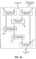
- DSP 36 manipulates the digital image data in its memory 32 according to a software program permanently stored in program memory 54 and copied to memory 32 for execution during image capture. DSP 36 executes the software necessary for practicing image processing shown in FIG. 18 .
- Memory 32 includes of any type of random access memory, such as SDRAM.
- a bus 30 comprising a pathway for address and data signals connects DSP 36 to its related memory 32, A/D converter 24 and other related devices.
- System controller 50 controls the overall operation of the camera based on a software program stored in program memory 54, which can include Flash EEPROM or other nonvolatile memory. This memory can also be used to store image sensor calibration data, user setting selections and other data which must be preserved when the camera is turned off.
- System controller 50 controls the sequence of image capture by directing exposure controller 40 to operate the lens 12, ND filter 13, iris 14, and shutter 18 as previously described, directing the timing generator 26 to operate the image sensor 20 and associated elements, and directing DSP 36 to process the captured image data. After an image is captured and processed, the final image file stored in memory 32 is transferred to a host computer via interface 57, stored on a removable memory card 64 or other storage device, and displayed for the user on image display 88.
- a bus 52 includes a pathway for address, data and control signals, and connects system controller 50 to DSP 36, program memory 54, system memory 56, host interface 57, memory card interface 60 and other related devices.
- Host interface 57 provides a high speed connection to a personal computer (PC) or other host computer for transfer of image data for display, storage, manipulation or printing.
- PC personal computer
- This interface is an IEEE1394 or USB2.0 serial interface or any other suitable digital interface.
- Memory card 64 is typically a Compact Flash (CF) card inserted into socket 62 and connected to the system controller 50 via memory card interface 60.
- CF Compact Flash
- Other types of storage that are utilized include without limitation PC-Cards, MultiMedia Cards (MMC), or Secure Digital (SD) cards.
- Processed images are copied to a display buffer in system memory 56 and continuously read out via video encoder 80 to produce a video signal.
- This signal is output directly from the camera for display on an external monitor, or processed by display controller 82 and presented on image display 88.
- This display is typically an active matrix color liquid crystal display (LCD), although other types of displays are used as well.
- the user interface including all or any combination of viewfinder display 70, exposure display 72, status display 76 and image display 88, and user inputs 74, is controlled by a combination of software programs executed on exposure controller 40 and system controller 50.
- User inputs 74 typically include some combination of buttons, rocker switches, joysticks, rotary dials or touchscreens.
- Exposure controller 40 operates light metering, exposure mode, autofocus and other exposure functions.
- the system controller 50 manages the graphical user interface (GUI) presented on one or more of the displays, e.g., on image display 88.
- the GUI typically includes menus for making various option selections and review modes for examining captured images.
- Exposure controller 40 accepts user inputs selecting exposure mode, lens aperture, exposure time (shutter speed), and exposure index or ISO speed rating and directs the lens and shutter accordingly for subsequent captures.
- Brightness sensor 16 is employed to measure the brightness of the scene and provide an exposure meter function for the user to refer to when manually setting the ISO speed rating, aperture and shutter speed. In this case, as the user changes one or more settings, the light meter indicator presented on viewfinder display 70 tells the user to what degree the image will be over or underexposed.
- an automatic exposure mode the user changes one setting and the exposure controller 40 automatically alters another setting to maintain correct exposure, e.g., for a given ISO speed rating when the user reduces the lens aperture the exposure controller 40 automatically increases the exposure time to maintain the same overall exposure.
- the ISO speed rating is an important attribute of a digital still camera.
- the exposure time, the lens aperture, the lens transmittance, the level and spectral distribution of the scene illumination, and the scene reflectance determine the exposure level of a digital still camera.
- proper tone reproduction can generally be maintained by increasing the electronic or digital gain, but the image will contain an unacceptable amount of noise.
- the gain is decreased, and therefore the image noise can normally be reduced to an acceptable level.
- the resulting signal in bright areas of the image can exceed the maximum signal level capacity of the image sensor or camera signal processing. This can cause image highlights to be clipped to form a uniformly bright area, or to bloom into surrounding areas of the image.
- An ISO speed rating is intended to serve as such a guide.
- the ISO speed rating for a digital still camera should directly relate to the ISO speed rating for photographic film cameras. For example, if a digital still camera has an ISO speed rating of ISO 200, then the same exposure time and aperture should be appropriate for an ISO 200 rated film/process system.
- the ISO speed ratings are intended to harmonize with film ISO speed ratings.
- Digital still cameras can include variable gain, and can provide digital processing after the image data has been captured, enabling tone reproduction to be achieved over a range of camera exposures. It is therefore possible for digital still cameras to have a range of speed ratings. This range is defined as the ISO speed latitude.
- a single value is designated as the inherent ISO speed rating, with the ISO speed latitude upper and lower limits indicating the speed range, that is, a range including effective speed ratings that differ from the inherent ISO speed rating.
- the inherent ISO speed is a numerical value calculated from the exposure provided at the focal plane of a digital still camera to produce specified camera output signal characteristics.
- the inherent speed is usually the exposure index value that produces peak image quality for a given camera system for normal scenes, where the exposure index is a numerical value that is inversely proportional to the exposure provided to the image sensor.
- the image sensor 20 shown in FIG. 1 typically includes a two-dimensional array of light sensitive pixels fabricated on a silicon substrate that provide a way of converting incoming light at each pixel into an electrical signal that is measured. As the sensor is exposed to light, free electrons are generated and captured within the electronic structure at each pixel. Capturing these free electrons for some period of time and then measuring the number of electrons captured, or measuring the rate at which free electrons are generated can measure the light level at each pixel. In the former case, accumulated charge is shifted out of the array of pixels to a charge to voltage measurement circuit as in a charge coupled device (CCD), or the area close to each pixel can contain elements of a charge to voltage measurement circuit as in an active pixel sensor (APS or CMOS sensor).
- CCD charge coupled device
- image sensor 20 Whenever general reference is made to an image sensor in the following description, it is understood to be representative of the image sensor 20 from FIG. 1 . It is further understood that all examples and their equivalents of image sensor architectures and pixel patterns of the present invention disclosed in this specification is used for image sensor 20.
- a pixel (a contraction of "picture element") refers to a discrete light sensing area and charge shifting or charge measurement circuitry associated with the light sensing area.
- the term pixel commonly refers to a particular location in the image having associated color values.
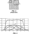
- FIG. 2 shows a pattern of red, green, and blue color filters that is commonly used.
- This particular pattern is commonly known as a Bayer color filter array (CFA) after its inventor Bryce Bayer as disclosed in US 3,971,065 .
- CFA Bayer color filter array
- This pattern is effectively used in image sensors having a two-dimensional array of color pixels.
- each pixel has a particular color photoresponse that, in this case, is a predominant sensitivity to red, green or blue light.
- Another useful variety of color photoresponses is a predominant sensitivity to magenta, yellow, or cyan light.
- the particular color photoresponse has high sensitivity to certain portions of the visible spectrum, while simultaneously having low sensitivity to other portions of the visible spectrum.
- the term color pixel will refer to a pixel having a color photoresponse.
- the set of color photoresponses selected for use in a sensor usually has three colors, as shown in the Bayer CFA, but it can also include four or more.
- a panchromatic photoresponse refers to a photoresponse having a wider spectral sensitivity than those spectral sensitivities represented in the selected set of color photoresponses.
- a panchromatic photosensitivity can have high sensitivity across the entire visible spectrum.
- panchromatic pixel will refer to a pixel having a panchromatic photoresponse.
- each panchromatic pixel can have an associated filter. Such filter is either a neutral density filter or a color filter.
- each such pattern has a repeating unit that is a contiguous subarray of pixels that acts as a basic building block.
- the entire sensor pattern is produced.
- the juxtaposition of the multiple copies of repeating units are done in diagonal directions as well as in the horizontal and vertical directions.
- a minimal repeating unit is a repeating unit such that no other repeating unit has fewer pixels.
- the CFA in FIG. 2 includes a minimal repeating unit that is two pixels by two pixels as shown by pixel block 100 in FIG. 2 . Multiple copies of this minimal repeating unit is tiled to cover the entire array of pixels in an image sensor.
- the minimal repeating unit is shown with a green pixel in the upper right corner, but three alternative minimal repeating units can easily be discerned by moving the heavy outlined area one pixel to the right, one pixel down, or one pixel diagonally to the right and down.
- pixel block 102 is a repeating unit, it is not a minimal repeating unit because pixel block 100 is a repeating unit and block 100 has fewer pixels than block 102.
- An image captured using an image sensor having a two-dimensional array with the CFA of FIG. 2 has only one color value at each pixel.
- CFA interpolation techniques are well known in the art and reference is made to the following patents: US5506619 , US5629734 , and US5652621 .
- FIG. 3 shows the relative spectral sensitivities of the pixels with red, green, and blue color filters in a typical camera application.
- the X-axis in FIG. 3 represents light wavelength in nanometers, and the Y-axis represents efficiency.
- curve 110 represents the spectral transmission characteristic of a typical filter used to block infrared and ultraviolet light from reaching the image sensor. Such a filter is needed because the color filters used for image sensors typically do not block infrared light, hence the pixels are unable to distinguish between infrared light and light that is within the passbands of their associated color filters.
- the infrared blocking characteristic shown by curve 110 prevents infrared light from corrupting the visible light signal.
- the spectral quantum efficiency i.e.
- panchromatic photoresponse is three to four times more sensitive to wide spectrum light than any of the color photoresponses.
- the greater panchromatic sensitivity shown in FIG. 3 permits improving the overall sensitivity of an image sensor by intermixing pixels that include color filters with pixels that do not include color filters.
- the color filter pixels will be significantly less sensitive than the panchromatic pixels.
- the panchromatic pixels are properly exposed to light such that the range of light intensities from a scene cover the full measurement range of the panchromatic pixels, then the color pixels will be significantly underexposed.
- the sensitivity of the color pixels are increased, for example, by increasing the size of the color pixels relative to the panchromatic pixels, with an associated reduction inspatial pixels.
- FIG. 4A represents a two-dimensional array of pixels having two groups. Pixels from the first group of pixels have a narrower spectral photoresponse than pixels from the second group of pixels.
- the first group of pixels includes individual pixels that relate to at least two different spectral photoresponses corresponding to at least two color filters. These two groups of pixels are intermixed to improve the overall sensitivity of the sensor.
- the placement of the first and second groups of pixels defines a pattern that has a minimal repeating unit including at least twelve pixels.
- the minimal repeating unit includes first and second groups of pixels arranged to permit the reproduction of a captured color image under different lighting conditions.
- the complete pattern shown in FIG. 4A represents a minimal repeating unit that is tiled to cover an entire array of pixels.
- FIG. 2 there are several other minimal repeating units that are used to describe this overall arrangement of color and panchromatic pixels, but they are all essentially equivalent in their characteristics and each is a subarray of pixels, the subarray being eight pixels by eight pixels in extent.
- An important feature of this pattern is alternating rows of panchromatic and color pixels with the color rows having pixels with the same color photoresponse grouped together.
- the groups of pixels with the same photoresponse along with some of their neighboring panchromatic pixels are considered to form four cells that make up the minimal repeating unit, a cell being a contiguous subarray of pixels having fewer pixels than a minimal repeating unit.
- These four cells delineated by heavy lines in FIG. 4A and shown as cells 120, 122, 124, and 126 in FIG. 5 , enclose four groups of four-by-four pixels each, with 120 representing the upper left cell, 122 representing the upper right cell, 124 representing the lower left cell, and 126 representing the lower right cell.
- Each of the four cells includes eight panchromatic pixels and eight color pixels of the same color photoresponse. The color pixels in a cell is combined to represent the color for that entire cell.
- cell 120 in FIG. 5 is considered to be a green cell
- cell 122 is considered to be a red cell, and so on.
- Each cell includes at least two pixels of the same color, thereby allowing pixels of the same color to be combined to overcome the difference in photosensitivity between the color pixels and the panchromatic pixels.
- the minimal repeating unit includes sixteen pixels. In the case of a minimal repeating unit with three non-overlapping cells, with each cell having two pixels of the same color and two panchromatic pixels, it is clear that the minimal repeating unit includes twelve pixels.
- the minimal repeating unit of FIG. 4A when considered in light of the cell structure identified in FIG. 5 , can represent the combination of a high-resolution panchromatic image and a low-resolution Bayer pattern color image arranged to permit the reproduction of a captured color image under different lighting conditions.
- the individual elements of the Bayer pattern image represent the combination of the color pixels in the corresponding cells.
- the first group of pixels defines a low-resolution color filter array image and the second group of pixels defines a high-resolution panchromatic image. See FIG. 6A and FIG. 6B.
- FIG. 6A represents the high-resolution panchromatic image corresponding to FIG. 4A , including both the panchromatic pixels P from FIG.
- FIG. 6B represents the low-resolution Bayer pattern color image, with R', G', and B' representing for each of the cells outlined in FIG. 5 the cell color associated with the combined color pixels in the cell.
- each cell of the pattern is rotated 90 degrees to produce the pattern shown in FIG. 4B .
- This is substantially the same pattern, but it places the highest panchromatic sampling frequency in the vertical direction instead of the horizontal direction.
- the choice to use FIG. 4A or FIG. 4B depends on whether or not it is desired to have higher panchromatic spatial sampling in either the horizontal or vertical directions respectively.
- FIG. 4A and FIG. 4B are equivalent from a color perspective.
- FIG. 4A and FIG. 4B are examples of practicing the present invention with the panchromatic pixels arranged linearly in either rows or columns.
- FIG. 4A has single rows of panchromatic pixels with each row separated from a neighboring row of panchromatic pixels by a row of color pixels;
- FIG. 4B has the same characteristic in the column direction.
- FIG. 4C represents yet another alternative minimal repeating unit to FIG. 4A with essentially the same cell color characteristics.
- FIG. 4C shows the panchromatic and color rows staggered on a cell by cell basis. This can improve the vertical panchromatic resolution.
- FIG. 4D Yet another alternative minimal repeating unit to FIG. 4A is represented in FIG. 4D , wherein the panchromatic and color rows are staggered by column pairs. This also has the potential of improving the vertical panchromatic resolution.
- a characteristic of all of the minimal repeating units of FIGS. 4A-D is that groups of two or more same color pixels are arranged side by side in either rows or columns.
- FIGS. 4A-D all have the same color structure with the cells that constitute the minimal repeating unit expressing a low-resolution Bayer pattern. It can therefore be seen that a variety of arrangements of panchromatic pixels and grouped color pixels are constructed within the scope of the present invention.
- the color pixels within each cell is combined in various ways. For example, the charge from same colored pixels are combined or binned in a CCD image sensor or in types of active pixel sensors that permit binning. Alternatively, the voltages corresponding to the measured amounts of charge in same colored pixels are averaged, for example by connecting in parallel capacitors that are charged to these voltages. In yet another approach, the digital representations of the light levels at same colored pixels are summed or averaged.
- Combining or binning charge from two pixels doubles the signal level, while the noise associated with sampling and reading out the combined signal remains the same, thereby increasing the signal to noise ratio by a factor of two, representing a corresponding two times increase in the photosensitivity of the combined pixels.
- the resulting signal increases by a factor of two, but the corresponding noise levels from reading the two pixels combine in quadrature, thereby increasing the noise by the square root of two; the resulting signal to noise ratio of the combined pixels therefore increases by the square root of two over the uncombined signals.
- a similar analysis applies to voltage or digital averaging.
- each R', G', and B' has twice the sensitivity of the uncombined pixels.
- vertically combining the charge from same colored pixels in groups of two as in FIG. 7A and horizontally summing or averaging the measured values of the combined pixels of FIG. 7A in groups of four produces the final combined color pixels of FIG. 7C , with R", G", and B" representing the final combinations of same coloured pixels.
- the final combined color pixels of FIG. 7C each have four times the sensitivity of the uncombined pixels.
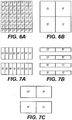
- FIG. 8A which illustrates an example that is not an embodiment of the present invention, but which is useful for understanding the present invention, shows the cyan, magenta, and yellow equivalent of FIG. 4A , with C representing cyan pixels, M representing magenta pixels, and Y representing yellow pixels.
- FIG. 8B which illustrates an example that is not an embodiment of the present invention, but which is useful for understanding the present invention, shows a minimal repeating unit of the present invention that includes cyan pixels (represented by C), magenta pixels (represented by M), yellow pixels (represented by Y), and green pixels (represented by G).
- FIG. 8C which illustrates an example that is not an embodiment of the present invention, but which is useful for understanding the present invention, shows yet another alternative four color arrangement including red pixels (represented by R), blue pixels (represented by B), green pixels with one color photoresponse (represented by G), and alternative green pixels with a different color photoresponse (represented by E).
- FIG. 8D which illustrates an example that is not an embodiment of the present invention, but which is useful for understanding the present invention, shows yet another alternative four color arrangement, wherein one of the green cells of FIG. 4A is replaced by a yellow cell, with the yellow pixels represented by Y.
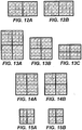
- FIG. 9 represents an alternative minimal repeating unit of the present invention with the same cell structure as FIG. 4A but with a checkerboard pattern of panchromatic pixels. This pattern provides uniform panchromatic sampling of the image, overcoming the vertical panchromatic sampling deficit of FIGS. 4A, 4C, and 4D .
- FIG. 9 is characterized as an example of practicing the present invention by arranging the panchromatic pixels in diagonal lines.
- FIG. 9 is further characterized as having single diagonal lines of panchromatic pixels with each diagonal line separated from a neighboring diagonal line of panchromatic pixels by a diagonal line of color pixels.
- Yet another characteristic of FIG. 9 is that groups two or more of same color pixels are arranged side by side in diagonal lines.
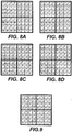
- FIG. 10A shows yet another embodiment of the present invention wherein color pixels are embedded within a grid pattern of panchromatic pixels. This pattern provides very good panchromatic spatial sampling while expressing the same color cell arrangement as FIG. 4A and 9 .
- FIG. 10B which illustrates an example that is not an embodiment of the present invention, but which is useful for understanding the present invention, provides an example of a four color embodiment of the panchromatic grid pattern.
- the minimal repeating unit of FIG. 10 is characterized as separating each color pixel from a neighboring color pixel by one or more panchromatic pixels.
- a minimal repeating unit has been previously defined as a repeating unit such that no other repeating unit has fewer pixels.
- the sizes of repeating units from different pixel patterns are compared according to the total number of pixels in the repeating unit.
- a repeating unit that is smaller than a repeating unit having eight pixels by eight pixels contains fewer than 64 total pixels.
- the patterns presented so far have exhibited a cell structure wherein each cell contains a single color in addition to panchromatic pixels. Furthermore, all the patterns presented so far have exhibited a minimal repeating unit that is eight by eight pixels in extent.
- a minimal repeating unit can also be used that has cells with more than one color in each cell; also, a minimal repeating unit is defined that is less than eight pixels by eight pixels in extent.
- the minimal repeating unit of FIG. 11A which illustrates an example that is not an embodiment of the present invention, but which is useful for understanding the present invention, has two cells with each cell including two colors: blue and green (represented by B and G respectively) in the left cell, and red and green (represented by R and G respectively) in the right cell.
- B and G blue and green
- R and G red and green
- FIG. 11A the cells contain two colors, and these colors are arranged to facilitate combining same colors for the purpose of improving color sensitivity.
- FIG. 11B which illustrates an example that is not an embodiment of the present invention, but which is useful for understanding the present invention, shows how the minimal repeating unit of FIG. 11A is tiled in order to stagger the red and blue colors.
- FIG. 11C which illustrates an example that is not an embodiment of the present invention, but which is useful for understanding the present invention, provides a minimal repeating unit employing four colors and two colors per cell.
- FIG. 11D which illustrates an example that is not an embodiment of the present invention, but which is useful for understanding the present invention, shows how the minimal repeating unit of FIG. 11C is tiled in order to stagger the red and blue colors.
- FIG. 11D the coarse color pattern is characterized as a checkerboard of two different color photoresponses in the green range (represented by G and E) interleaved with a checkerboard of red and blue (represented by R and B, respectively).
- FIG. 12A which illustrates an example that is not an embodiment of the present invention, but which is useful for understanding the present invention, provides a panchromatic checkerboard version of FIG. 11A
- FIG. 12B which illustrates an example that is not an embodiment of the present invention, but which is useful for understanding the present invention, provides a panchromatic checkerboard version of FIG. 11C .
- the minimal repeating units of FIGS. 11A and 11C are characterized as separating each color pixel from a neighbouring color pixel in rows and columns by a dissimilar pixel, either a different color pixel or a panchromatic pixel.
- FIG. 13A is analogous to FIG. 4A , but with each color cell being 3 pixels wide by 4 pixels high and with the overall minimal repeating unit being 6 pixels wide by 8 pixels high.
- FIG. 13B eliminates two of the color pixel rows from FIG. 13A , thereby producing cells that are 3 pixels by 3 pixels and a minimal repeating unit that is 6 pixels by 6 pixels.
- FIG. 13C goes further by eliminating two of the panchromatic rows, thereby producing cells that are 3 pixels wide by 2 pixels high (with each cell containing 3 panchromatic pixels and 3 color pixels) and a minimal repeating unit that is 6 pixels wide by 4 pixels tall.
- the patterns shown in FIGS. 13A through 13C are particularly usable if the scheme for combining colors within each cell requires less than the numbers of pixels shown in FIG. 4A and other patterns.
- FIG. 14A shows yet another minimal repeating unit.
- the minimal repeating unit in FIG. 14A is six pixels by six pixels, with each cell including a 4 pixel diamond pattern of a single color with the remaining 5 pixels being panchromatic pixels.
- the panchromatic spatial sampling pattern shown in FIG. 14A is somewhat irregular, suggesting the pattern of FIG. 14B with a panchromatic checkerboard and the remaining pixels in each three pixel by three pixel cell occupied by a single color.
- FIG. 15A shows a minimal repeating unit that is four by four pixels and includes four two by two pixel cells. Note that each cell includes two panchromatic pixels and two same color pixels. The invention requires the placement of two same color pixels in each of the two by two cells in order to facilitate combining the color pixels within each cell.
- FIG. 15B is similar to FIG. 15A but employs a panchromatic checkerboard pattern.
- FIG. 16 the minimal repeating unit of FIG. 5 is shown subdivided into four cells, a cell being a contiguous subarray of pixels having fewer pixels than a minimal repeating unit.
- the software needed to provide the following processing is included in DSP 36 of FIG. 1 .
- Cells 220, 224, 226, and 228 are examples of cells wherein these cells contain pixels having green, red, blue and green photoresponses, respectively.
- cell 220 contains both panchromatic pixels and green pixels, the green pixels being identified as pixel group 222.
- the eventual goal is to produce a single green signal for cell 220 by combining the eight green signals from the green pixels in pixel group 222.
- a single green signal is produced by combining all eight green signals in the analog domain (e.g. by charge binning), or multiple green signals are produce by combining smaller groups of pixels taken from pixel group 222.
- the panchromatic pixels of cell 220 are shown in FIG. 17A . In the following examples, all eight signals from these panchromatic pixels are individually digitized.
- the green pixels of cell 220 are shown in FIGS. 17B-17E wherein they are grouped together according to how their signals are combined in the analog domain.
- FIG. 17B depicts the case in which all eight green pixels are combined to produce a single green signal for cell 220 ( FIG. 16 ).
- the sensor can produce two green signals, for example, by first combining the signals from pixels G21, G22, G23, and G24, and then combining the signals from pixels G41, G42, G43, and G44, as shown in FIG. 17C .
- Two signals are produced in other ways as well.
- the sensor can first combine signals from pixels G21, G22, G41, and G42, and then combine signals from pixels G23, G24, G43, and G44, as shown in FIG. 17D .
- the sensor can also produce four green signals for cell 220 by combining four pairs of signals, for example, combining pixels G21 with G22, then combining G23 with G24, then combining G41 with G42, and finally combining G43 with G44, as shown in FIG. 17E .
- cells 224, 226, and 228 For cells 224, 226, and 228 ( FIG 16 ), similar color signals are produced by the sensor depending on its mode of operation.
- the color signals for cells 224, 226, and 228 are red, blue, and green, respectively.
- the image processing algorithm of the present invention further combines the digitized green values to produce a single green value for the cell.
- One way that a single green value is obtained is by averaging all the digitized green values produced for cell 220.
- all the color data within the cell is similarly combined so that there is a single value for each color photoresponse represented within the cell.
- the digital signal processor block 36 ( FIG. 1 ) is shown receiving captured raw image data from the data bus 30 ( FIG. 1 ).
- the raw image data is passed to both the Low-resolution Partial Color block 202 and the High-resolution Panchrome block 204.
- An example of a minimal repeating unit for an image sensor has already been shown in FIG. 5 and FIG. 16 .
- the captured raw image data includes the panchromatic data that is produced by the individual panchromatic pixels as shown in FIG 17A .
- one or more green (color) values are also included, for example, from the combinations shown in FIGS. 17B-E .
- a partial color image is produced from the captured raw image data, a partial color image being a color image wherein each pixel has at least one color value and each pixel is also missing at least one color value.
- the captured raw data contains some number of color values produced by the color pixels within each cell.
- these color values are reduced to a single value for each color represented within the cell. For the cell 220 ( FIG. 16 ), as an example, a single green color value is produced.
- cells 224, 226 and 228, a single red, blue and green color value is produced, respectively.
- the Low-resolution Partial Color block 202 processes each cell in a similar manner resulting in an array of color values, one for each cell. Because the resulting image array based on cells rather than pixels in the original sensor, it is four times smaller in each dimension than the original captured raw image data array. Because the resulting array is based on cells and because each pixel has some but not all color values, the resulting image is a low-resolution partial color image. At this point, the low-resolution partial color image is color balanced.
- panchromatic values must be estimated for the green pixels in pixel group 222 ( FIG. 16 ).
- One simple way to estimate the missing panchromatic values is to do vertical averaging.
- P 22 P 12 + P 32 / 2
- An adaptive method can also be used.
- panchromatic interpolation is continued throughout the image without regard to cell boundaries.
- the processing of High-resolution Panchrome block 204 is done, the resulting digital panchromatic image is the same size as the original captured raw image, which makes it a high-resolution panchromatic image.
- the Low-resolution Panchrome block 206 receives the high-resolution panchromatic image array produced by block 204 and generates a low-resolution panchromatic image array which is the same size as the low-resolution partial color image produced by block 202.
- Each low-resolution panchromatic value is obtained by averaging the estimated panchromatic values, within a given cell, for those pixels having color filters.
- the high-resolution panchromatic values previously estimated for the green pixels in pixel group 222 ( FIG. 16 ) are now averaged together to produce a single low-resolution panchromatic value for the cell.
- a single low-resolution panchromatic value is computed for cell 224 using high-resolution panchromatic values estimated at the pixels having red filters. In this manner, each cell ends up with a single low-resolution panchromatic value.
- the Low-resolution Color Difference block 208 receives the low-resolution partial color image from block 202 and the low-resolution panchrome array from block 206. A low-resolution intermediate color image is then formed by color interpolating the low-resolution partial color image with guidance from the low-resolution panchrome image. The exact nature of the color interpolation algorithm, to be discussed in detail later, depends on which pattern of pixel photoresponses was used to capture the original raw image data.
- the High-resolution Color Difference block 210 receives the low-resolution color difference image from block 208 and, using bilinear interpolation, upsamples the low-resolution color difference image to match the size of the original raw image data. The result is a high-resolution color difference image that is the same size as the high-resolution panchromatic image produced by block 204.
- the High-resolution Final Image block 212 receives the high-resolution color difference image from block 210 and the high-resolution panchromatic image from block 204.
- a high-resolution final color image is then formed by adding the high-resolution panchromatic image to each of the high-resolution color difference planes.
- the resulting high-resolution final color image can then be further processed. For example, it is stored in the DSP Memory block 32 ( FIG. 1 ) and then sharpened and compressed for storage on the Memory Card block 64 ( FIG. 1 ).
- the sensor filter patterns shown in FIGS. 4A-D , 8A , 9 , 10A , 13A-C, 14A-B and 15A-B have a minimal repeating unit such that the resulting low-resolution partial color image, produced in block 202, exhibits the repeating Bayer pattern for color filters: G R B G
- every cell In addition to a single color value, given by the low-resolution partial color image, every cell also has a panchromatic value given by the low-resolution panchromatic image.
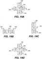
- Color interpolation begins by interpolating the green values at pixels not already having green values, shown as pixel234 in FIG. 19A .
- the four neighboring pixels shown as pixels 230, 232, 236, and 238, all have green values and they also all have panchromatic values.
- the center pixel 234 has a panchromatic value, but does not have a green value as indicated by the question marks.
- the first step is to compute two classifier values, the first relating to the horizontal direction, and the second to the vertical direction:
- HCLAS ABS P 4 ⁇ P 2 + ABS 2 * P 3 ⁇ P 2 ⁇ P 4
- VCLAS ABS P5 ⁇ P 1 + ABS 2 * P 3 ⁇ P1 ⁇ P5
- THRESH be an empirically determined threshold value
- pixel 252 is missing a red value and its two vertical neighbors, pixels 250 and 254, have red values R1 and R5 respectively.
- the low-resolution color differences can now be computed by subtracting the low-resolution panchrome values from each color plane: red, green, and blue in the example just discussed.
- the sensor pattern shown in FIG. 11A determines that each cell receives two color values: either green and red, or green and blue. Consequently, in this case, the color interpolation task within the Low-resolution Color Differences block 208 ( FIG. 18 ) estimates missing values of red or missing values of blue for each pixel.
- a pixel 264 is shown having a green value (G3) but not having a red value (R3).
- R3 red value
- Four of the neighboring pixels 260, 262, 266, and 268 have green values and red values.
- the method for interpolating the red value for pixel 264 ( FIG. 19D ) is similar to the method used to interpolate the green value for pixel 234 ( FIG. 19A ).
- the first step is to compute two classifier values, the first relating to the horizontal direction, and the second to the vertical direction:
- HCLAS ABS G4 ⁇ G 2 + ABS 2 * G 3 ⁇ G 2 ⁇ G 4
- VCLAS ABS G 5 ⁇ G 1 + ABS 2 * G 3 ⁇ G 1 ⁇ G 5
- HPRED R 4 + R 2 2 + 2 * G 3 ⁇ G 2 ⁇ G 4 / 2
- VPRED R 5 + R 1 / 2 + 2 * G 3 ⁇ G 1 ⁇ G 5 / 2
- the missing value G3 is computed adaptively according to:
- the missing blue values are interpolated in exactly the same way using blue values in place of red.
- the low-resolution intermediate color image has been produced. From there, the low-resolution color differences are computed as previously described.
Landscapes
- Engineering & Computer Science (AREA)
- Multimedia (AREA)
- Signal Processing (AREA)
- Physics & Mathematics (AREA)
- Spectroscopy & Molecular Physics (AREA)
- Color Television Image Signal Generators (AREA)
- Solid State Image Pick-Up Elements (AREA)
- Facsimile Heads (AREA)
Description
- This invention relates to a two-dimensional image sensor with improved light sensitivity
- An electronic imaging system depends on an electronic image sensor to create an electronic representation of a visual image. Examples of such electronic image sensors include charge coupled device (CCD) image sensors and active pixel sensor (APS) devices (APS devices are often referred to as CMOS sensors because of the ability to fabricate them in a Complementary Metal Oxide Semiconductor process). Typically, these images sensors include a number of light sensitive pixels, often arranged in a regular pattern of rows and columns. For capturing color images, a pattern of filters is typically fabricated on the pattern of pixels, with different filter materials being used to make individual pixels sensitive to only a portion of the visible light spectrum. The color filters necessarily reduce the amount of light reaching each pixel, and thereby reduce the light sensitivity of each pixel. A need persists for improving the light sensitivity, or photographic speed, of electronic color image sensors to permit images to be captured at lower light levels or to allow images at higher light levels to be captured with shorter exposure times.
- Image sensors are either linear or two-dimensional. Generally, these sensors have two different types of applications. The two-dimensional sensors are typically suitable for image capture devices such as digital cameras, cell phones and other applications. Linear sensors are often used for scanning documents. In either case, when color filters are employed the image sensors have reduced sensitivity.
- A linear image sensor, the KLI-4104 manufactured by Eastman Kodak Company, includes four linear, single pixel wide arrays of pixels, with color filters applied to three of the arrays to make each array sensitive to either red, green, or blue in its entirety, and with no color filter array applied to the fourth array; furthermore, the three color arrays have larger pixels to compensate for the reduction in light sensitivity due to the color filters, and the fourth array has smaller pixels to capture a high resolution monochrome image. When an image is captured using this image sensor, the image is represented as a high resolution, high photographic sensitivity monochrome image along with three lower resolution images with roughly the same photographic sensitivity and with each of the three images corresponding to either red, green, or blue light from the image; hence, each point in the electronic image includes a monochrome value, a red value, a green value, and a blue value. However, since this is a linear image sensor, it requires relative mechanical motion between the image sensor and the image in order to scan the image across the four linear arrays of pixels. This limits the speed with which the image is scanned and precludes the use of this sensor in a handheld camera or in capturing a scene that includes moving objects.
- There is also known in the art an electronic imaging system described in
US Patent 4,823,186 by Akira Muramatsu that includes two sensors, wherein each of the sensors includes a two-dimensional array of pixels but one sensor has no color filters and the other sensor includes a pattern of color filters included with the pixels, and with an optical beam splitter to provide each image sensor with the image. Since the color sensor has a pattern of color filters applied, each pixel in the color sensor provides only a single color. When an image is captured with this system, each point in the electronic image includes a monochrome value and one color value, and the color image must have the missing colors at each pixel location interpolated from the nearby colors. Although this system improves the light sensitivity over a single conventional image sensor, the overall complexity, size, and cost of the system is greater due to the need for two sensors and a beam splitter. Furthermore, the beam splitter directs only half the light from the image to each sensor, limiting the improvement in photographic speed. - In addition to the linear image sensor mentioned above, there are known in the art image sensors with two-dimensional arrays of pixels where the pixels include pixels that do not have color filters applied to them. For example, see
Sato et al in US Patent 4,390,895 ,Yamagami et al in US Patent 5,323,233 , andGindele et al in US Patent 6,476,865 . In each of the cited patents, the sensitivity of the unfiltered or monochrome pixels is significantly higher than the color pixels, requiring the application of gain to the color pixels in order to match the color and monochrome signals from the pixel array. Increasing gain increases noise as well as signal, causing degradation in the overall signal to noise ratio of the resulting image. Frame inUS Patent Application 2003/0210332 discloses a pixel array with most of the pixels being unfiltered, but the color pixels suffer from the same sensitivity deficit as mentioned above. - Therefore, there persists a need for improving the light sensitivity for electronic capture devices that employ a single sensor with a two-dimensional array of pixels.
-
US 4,437,112 discloses a solid-state color imaging apparatus which comprises an imaging device composed of a solid-state charge-coupled device having a plurality of cells each of which has at least two potential wells and color filter having a combination of color filter elements which are positioned corresponding to the two potential wells in such a manner as to provide different spectral sensitivities to the two potential wells. -
GB2105143 -
EP0472299 discloses an image signal processing apparatus which comprises an image pickup device with color filter means having a set of luminance portions for passing a luminance component located in an offset manner and a plurality of sets of color portions for passing different color components from each other, wherein the portions of at least one color set are located in an offset manner to improve the effective resolution of the corresponding color component. The apparatus generates color difference signals from the color component signals independently of the luminance component signal, or alternatively the color portions of the filter have a high transparency, in either case to reduce the tendency of false color difference signals to be generated owing to saturation of some but not all of the signals used to generate a color difference signal.; The filter portions may be arranged in pairs of adjacent rows having the same pattern of filter portions, for use with a pickup device with interlace scan. -
EP0119862 discloses an array of picture elements in rows ℓ1, ℓ2, etc. that provides inputs to vertical charge coupled device (CCD) registers which feed into a horizontal CCD register which feed into a horizontal CCD register which provides the video output. In even fields transfers are made from even rows ℓ2, ℓ4, etc. and then, after a one element shift from odd rows ℓ1, ℓ3, etc. so that combined signals ℓ1 + ℓ2, ℓ3 + ℓ4, etc. are formed. Similarly in even fields the combined signals are ℓ2 + ℓ3, ℓ4 + ℓ5, etc. The elements have colour filters establishing a 2-element horizontal by 4-element vertical repeat pattern wherein a green component comes from all elements whereas red and blue components are modulated at a 2-element horizontal rate with a line to line phase alternation applying to one of these components, but not the other. In accordance with the invention the said pattern is established using transparent (W), green (G), yellow (Ye) and cyan (Cy) filters, where transparent passes all components, yellow passes red and green and cyan passes blue and green. Every row has at least one filter passing red and at least one passing blue within each 2 by 4 pattern block but the modulation of red and blue is retained as red components pass only alternate filters in odd lines (with phase alternation) whereas blue components pass only alternate filters in even lines (without phase alternation). -
US2004046881 discloses an imaging device which includes a plurality of photosensors arranged in matrix on a light-receiving surface and a readout section for adding up photo signals on the photosensors for external output in each pixel block set on the light-receiving surface. The pixel blocks each consist of N (N>=2) photosensors assembled in an array direction of the matrix and the pixel blocks in even number arrays and those in odd number arrays in the matrix are shifted from each other by half a phase in the array direction. With or without execution of the adding-up operation, it is able to switch a pattern of readout pixels from the imaging device between a grid pattern and a diagonal grid pattern. - The present invention is directed to providing an image sensor having a two-dimensional array of color and panchromatic pixels that provides high sensitivity and is effective in producing full color images.
- The present invention provides an image capture device as set out in claim 1.
- Image sensors in accordance with the present invention are particularly suitable for low level lighting conditions, where such low level lighting conditions are the result of low scene lighting, short exposure time, small aperture, or other restrictions on light reaching the sensor. They have a broad application and numerous types of image capture devices can effectively use these sensors.
- These and other aspects, objects, features and advantages of the present invention will be more clearly understood and appreciated from a review of the following detailed description of the preferred embodiments and appended claims, and by reference to the accompanying drawings.
-
-
FIG. 1 is a block diagram of a conventional digital still camera system that can employ a conventional sensor and processing methods of the sensor and processing methods of the current invention; -
FIG. 2 (prior art) is conventional Bayer color filter array pattern showing a minimal repeating unit and a non-minimal repeating unit; -
FIG. 3 provides representative spectral quantum efficiency curves for red, green, and blue pixels, as well as a wider spectrum panchromatic quantum efficiency, all multiplied by the transmission characteristics of an infrared cut filter; -
FIGS. 4A-D provides minimal repeating units for several variations of a color filter array pattern of the present invention that has color pixels with the same color photo response arranged in rows or columns; -
FIG. 5 shows the cell structure of the minimal repeating unit fromFIG. 4A ; -
FIG. 6A is the interpolated panchromatic image forFIG. 4A ; -
FIG. 6B is the low-resolution color image corresponding to the cells inFIG. 4A and FIG. 5 ; -
FIGS. 7A-C shows several ways of combining the pixels ofFIG. 4A ; -
FIGS. 8A-D , which illustrate examples that are not embodiments of the present invention, but which are useful for understanding the present invention, show the color filter array pattern ofFIG. 4A with color pixels that have alternative color photoresponse characteristics, including four color alternatives as well as cyan, magenta, and yellow alternatives; -
FIG. 9 provides a minimal repeating unit for an alternative color filter array of the present invention in which the panchromatic pixels are arranged in diagonal lines; -
FIGS. 10A-B provides minimal repeating units for two variations of an alternative color filter array in which the
panchromatic pixels form a grid into which the color pixels are embedded, whereinFIG. 10A is in accordance with the present invention andFIG. 10B is not in accordance with the present invention but is useful for understanding the present invention; -
FIGS. 11A-D , which illustrate examples that are not embodiments of the present invention, but which are useful for understanding the present invention, provides minimal repeating units and tiling arrangements for two variations of an alternative color filter array of the present invention in which there are two colors per cell; -
FIGS. 12A-B , which illustrate examples that are not embodiments of the present invention, but which are useful for understanding the present invention, provides minimal repeating units for two variations of an alternative color filter array of the present invention in which there are two colors per cell and the panchromatic pixels are arranged in diagonal lines; -
FIGS. 13A-C provides variations ofFIG. 4A in which the minimal repeating unit is smaller than eight by eight pixels; -
FIGS. 14A-B provides minimal repeating units for two variations of an alternative color filter array of the present invention in which the minimal repeating unit is six by six pixels; -
FIGS. 15A-B provides minimal repeating units for two variations of an alternative color filter array of the present invention in which the minimal repeating unit is four by four pixels; -
FIG. 16 is the minimal repeating unit ofFIG. 4A which subscripts for individual pixels within the minimal repeating unit; -
FIGS. 17A-E shows the panchromatic pixels and the color pixels of one cell ofFIG. 16 , and various ways in which the color pixels are combined; -
FIG. 18 is a process diagram of the present invention showing the method of processing the color and panchromatic pixel data from a sensor of the present invention; and -
FIGS. 19A-D illustrates methods of the present invention for interpolating missing colors in the low-resolution partial color image ofFIG. 18 . - Because digital cameras employing imaging devices and related circuitry for signal capture and correction and for exposure control are well known, the present description will be directed in particular to elements forming part of, or cooperating more directly with, method and apparatus in accordance with the present invention. Elements not specifically shown or described herein are selected from those known in the art. Certain aspects of the embodiments to be described are provided in software. Given the system as shown and described according to the invention in the following materials, software not specifically shown, described or suggested herein that is useful for implementation of the invention is conventional and within the ordinary skill in such arts.
- Turning now to
FIG. 1 , a block diagram of an image capture device shown as a digital camera embodying the present invention is shown. Although a digital camera will now be explained, the present invention is clearly applicable to other types of image capture devices. In the disclosed camera, light 10 from the subject scene is input to animaging stage 11, where the light is focused bylens 12 to form an image on solidstate image sensor 20.Image sensor 20 converts the incident light to an electrical signal for each picture element (pixel). Theimage sensor 20 of the preferred embodiment is a charge coupled device (CCD) type or an active pixel sensor (APS) type (APS devices are often referred to as CMOS sensors because of the ability to fabricate them in a Complementary Metal Oxide Semiconductor process), Other types of image sensors having two-dimensional array of pixels are used provided that they employ the patterns of the present invention. The present invention also makes use of animage sensor 20 having a two-dimensional array of color and panchromatic pixels as will become clear later in this specification afterFIG. 1 is described. Examples of the patterns of color and panchromatic pixels of the present invention that are used with theimage sensor 20 are seen inFIGS. 4A-D ,FIGS. 8A-D ,FIG. 9 ,FIGS. 10A-B ,FIG. 11A, FIG. 11C ,FIGS. 13A-C, FIGS. 14A-B, and FIGS. 15A-B , although other patterns are used within the scope of the present invention. - The amount of light reaching the
sensor 20 is regulated by aniris block 14 that varies the aperture and the neutral density (ND)filter block 13 that
includes one or more ND filters interposed in the optical path. Also regulating the overall light level is the time that theshutter block 18 is open. Theexposure controller block 40 responds to the amount of light available in the scene as metered by thebrightness sensor block 16 and controls all three of these regulating functions. - This description of a particular camera configuration will be familiar to one skilled in the art, and it will be obvious that many variations and additional features are present. For example, an autofocus system is added, or the lens are detachable and interchangeable. It will be understood that the present invention is applied to any type of digital camera, where similar functionality is provided by alternative components. For example, the digital camera is a relatively simple point and shoot digital camera, where the
shutter 18 is a relatively simple movable blade shutter, or the like, instead of the more complicated focal plane arrangement. The present invention can also be practiced on imaging components included in non-camera devices such as mobile phones and automotive vehicles. - The analog signal from
image sensor 20 is processed byanalog signal processor 22 and applied to analog to digital (A/D)converter 24. Timinggenerator 26 produces various clocking signals to select rows and pixels and synchronizes the operation ofanalog signal processor 22 and A/D converter 24. Theimage sensor stage 28 includes theimage sensor 20, theanalog signal processor 22, the A/D converter 24, and thetiming generator 26. The components ofimage sensor stage 28 is separately fabricated integrated circuits, or they are fabricated as a single integrated circuit as is commonly done with CMOS image sensors. The resulting stream of digital pixel values from A/D converter 24 is stored inmemory 32 associated with digital signal processor (DSP) 36. -
Digital signal processor 36 is one of three processors or controllers in this embodiment, in addition tosystem controller 50 andexposure controller 40. Although this partitioning of camera functional control among multiple controllers and processors is typical, these controllers or processors are combined in various ways without affecting the functional operation of the camera and the application of the present invention. These controllers or processors can comprise one or more digital signal processor devices, microcontrollers, programmable logic devices, or other digital logic circuits. Although a combination of such controllers or processors has been described, it should be apparent that one controller or processor is designated to perform all of the needed functions. All of these variations can perform the same function and fall within the scope of this invention, and the term "processing stage" will be used as needed to encompass all of this functionality within one phrase, for example, as in processingstage 38 inFIG. 1 . - In the illustrated embodiment,
DSP 36 manipulates the digital image data in itsmemory 32 according to a software program permanently stored inprogram memory 54 and copied tomemory 32 for execution during image capture.DSP 36 executes the software necessary for practicing image processing shown inFIG. 18 .Memory 32 includes of any type of random access memory, such as SDRAM. Abus 30 comprising a pathway for address and data signals connectsDSP 36 to itsrelated memory 32, A/D converter 24 and other related devices. -
System controller 50 controls the overall operation of the camera based on a software program stored inprogram memory 54, which can include Flash EEPROM or other nonvolatile memory. This memory can also be used to store image sensor calibration data, user setting selections and other data which must be preserved when the camera is turned off.System controller 50 controls the sequence of image capture by directingexposure controller 40 to operate thelens 12,ND filter 13,iris 14, and shutter 18 as previously described, directing thetiming generator 26 to operate theimage sensor 20 and associated elements, and directingDSP 36 to process the captured image data. After an image is captured and processed, the final image file stored inmemory 32 is transferred to a host computer viainterface 57, stored on aremovable memory card 64 or other storage device, and displayed for the user onimage display 88. - A
bus 52 includes a pathway for address, data and control signals, and connectssystem controller 50 toDSP 36,program memory 54,system memory 56,host interface 57,memory card interface 60 and other related devices.Host interface 57 provides a high speed connection to a personal computer (PC) or other host computer for transfer of image data for display, storage, manipulation or printing. This interface is an IEEE1394 or USB2.0 serial interface or any other suitable digital interface.Memory card 64 is typically a Compact Flash (CF) card inserted intosocket 62 and connected to thesystem controller 50 viamemory card interface 60. Other types of storage that are utilized include without limitation PC-Cards, MultiMedia Cards (MMC), or Secure Digital (SD) cards. - Processed images are copied to a display buffer in
system memory 56 and continuously read out viavideo encoder 80 to produce a video signal. This signal is output directly from the camera for display on an external monitor, or processed bydisplay controller 82 and presented onimage display 88. This display is typically an active matrix color liquid crystal display (LCD), although other types of displays are used as well. - The user interface, including all or any combination of
viewfinder display 70,exposure display 72,status display 76 andimage display 88, anduser inputs 74, is controlled by a combination of software programs executed onexposure controller 40 andsystem controller 50.User inputs 74 typically include some combination of buttons, rocker switches, joysticks, rotary dials or touchscreens.Exposure controller 40 operates light metering, exposure mode, autofocus and other exposure functions. Thesystem controller 50 manages the graphical user interface (GUI) presented on one or more of the displays, e.g., onimage display 88. The GUI typically includes menus for making various option selections and review modes for examining captured images. -
Exposure controller 40 accepts user inputs selecting exposure mode, lens aperture, exposure time (shutter speed), and exposure index or ISO speed rating and directs the lens and shutter accordingly for subsequent captures.Brightness sensor 16 is employed to measure the brightness of the scene and provide an exposure meter function for the user to refer to when manually setting the ISO speed rating, aperture and shutter speed. In this case, as the user changes one or more settings, the light meter indicator presented onviewfinder display 70 tells the user to what degree the image will be over or underexposed. In an automatic exposure mode, the user changes one setting and theexposure controller 40 automatically alters another setting to maintain correct exposure, e.g., for a given ISO speed rating when the user reduces the lens aperture theexposure controller 40 automatically increases the exposure time to maintain the same overall exposure. - The ISO speed rating is an important attribute of a digital still camera. The exposure time, the lens aperture, the lens transmittance, the level and spectral distribution of the scene illumination, and the scene reflectance determine the exposure level of a digital still camera. When an image from a digital still camera is obtained using an insufficient exposure, proper tone reproduction can generally be maintained by increasing the electronic or digital gain, but the image will contain an unacceptable amount of noise. As the exposure is increased, the gain is decreased, and therefore the image noise can normally be reduced to an acceptable level. If the exposure is increased excessively, the resulting signal in bright areas of the image can exceed the maximum signal level capacity of the image sensor or camera signal processing. This can cause image highlights to be clipped to form a uniformly bright area, or to bloom into surrounding areas of the image. It is important to guide the user in setting proper exposures. An ISO speed rating is intended to serve as such a guide. In order to be easily understood by photographers, the ISO speed rating for a digital still camera should directly relate to the ISO speed rating for photographic film cameras. For example, if a digital still camera has an ISO speed rating of ISO 200, then the same exposure time and aperture should be appropriate for an ISO 200 rated film/process system.
- The ISO speed ratings are intended to harmonize with film ISO speed ratings. However, there are differences between electronic and film-based imaging systems that preclude exact equivalency. Digital still cameras can include variable gain, and can provide digital processing after the image data has been captured, enabling tone reproduction to be achieved over a range of camera exposures. It is therefore possible for digital still cameras to have a range of speed ratings. This range is defined as the ISO speed latitude. To prevent confusion, a single value is designated as the inherent ISO speed rating, with the ISO speed latitude upper and lower limits indicating the speed range, that is, a range including effective speed ratings that differ from the inherent ISO speed rating. With this in mind, the inherent ISO speed is a numerical value calculated from the exposure provided at the focal plane of a digital still camera to produce specified camera output signal characteristics. The inherent speed is usually the exposure index value that produces peak image quality for a given camera system for normal scenes, where the exposure index is a numerical value that is inversely proportional to the exposure provided to the image sensor.
- The foregoing description of a digital camera will be familiar to one skilled in the art. It will be obvious that there are many variations of this embodiment that are possible and is selected to reduce the cost, add features or improve the performance of the camera. The following description will disclose in detail the operation of this camera for capturing images according to the present invention. Although this description is with reference to a digital camera, it will be understood that the present invention applies for use with any type of image capture device having an image sensor with color and panchromatic pixels.
- The
image sensor 20 shown inFIG. 1 typically includes a two-dimensional array of light sensitive pixels fabricated on a silicon substrate that provide a way of converting incoming light at each pixel into an electrical signal that is measured. As the sensor is exposed to light, free electrons are generated and captured within the electronic structure at each pixel. Capturing these free electrons for some period of time and then measuring the number of electrons captured, or measuring the rate at which free electrons are generated can measure the light level at each pixel. In the former case, accumulated charge is shifted out of the array of pixels to a charge to voltage measurement circuit as in a charge coupled device (CCD), or the area close to each pixel can contain elements of a charge to voltage measurement circuit as in an active pixel sensor (APS or CMOS sensor). - Whenever general reference is made to an image sensor in the following description, it is understood to be representative of the
image sensor 20 fromFIG. 1 . It is further understood that all examples and their equivalents of image sensor architectures and pixel patterns of the present invention disclosed in this specification is used forimage sensor 20. - In the context of an image sensor, a pixel (a contraction of "picture element") refers to a discrete light sensing area and charge shifting or charge measurement circuitry associated with the light sensing area. In the context of a digital color image, the term pixel commonly refers to a particular location in the image having associated color values.
- In order to produce a color image, the array of pixels in an image sensor typically has a pattern of color filters placed over them.
FIG. 2 shows a pattern of red, green, and blue color filters that is commonly used. This particular pattern is commonly known as a Bayer color filter array (CFA) after its inventorBryce Bayer as disclosed in US 3,971,065 . This pattern is effectively used in image sensors having a two-dimensional array of color pixels. As a result, each pixel has a particular color photoresponse that, in this case, is a predominant sensitivity to red, green or blue light. Another useful variety of color photoresponses is a predominant sensitivity to magenta, yellow, or cyan light. In each case, the particular color photoresponse has high sensitivity to certain portions of the visible spectrum, while simultaneously having low sensitivity to other portions of the visible spectrum. The term color pixel will refer to a pixel having a color photoresponse. - The set of color photoresponses selected for use in a sensor usually has three colors, as shown in the Bayer CFA, but it can also include four or more. As used herein, a panchromatic photoresponse refers to a photoresponse having a wider spectral sensitivity than those spectral sensitivities represented in the selected set of color photoresponses. A panchromatic photosensitivity can have high sensitivity across the entire visible spectrum. The term panchromatic pixel will refer to a pixel having a panchromatic photoresponse. Although the panchromatic pixels generally have a wider spectral sensitivity than the set of color photoresponses, each panchromatic pixel can have an associated filter. Such filter is either a neutral density filter or a color filter.
- When a pattern of color and panchromatic pixels is on the face of an image sensor, each such pattern has a repeating unit that is a contiguous subarray of pixels that acts as a basic building block. By juxtaposing multiple copies of the repeating unit, the entire sensor pattern is produced. The juxtaposition of the multiple copies of repeating units are done in diagonal directions as well as in the horizontal and vertical directions.
- A minimal repeating unit is a repeating unit such that no other repeating unit has fewer pixels. For example, the CFA in
FIG. 2 includes a minimal repeating unit that is two pixels by two pixels as shown bypixel block 100 inFIG. 2 . Multiple copies of this minimal repeating unit is tiled to cover the entire array of pixels in an image sensor. The minimal repeating unit is shown with a green pixel in the upper right corner, but three alternative minimal repeating units can easily be discerned by moving the heavy outlined area one pixel to the right, one pixel down, or one pixel diagonally to the right and down. Althoughpixel block 102 is a repeating unit, it is not a minimal repeating unit becausepixel block 100 is a repeating unit and block 100 has fewer pixels thanblock 102. - An image captured using an image sensor having a two-dimensional array with the CFA of
FIG. 2 has only one color value at each pixel. In order to produce a full color image, there are a number of techniques for inferring or interpolating the missing colors at each pixel. These CFA interpolation techniques are well known in the art and reference is made to the following patents:US5506619 ,US5629734 , andUS5652621 . -
FIG. 3 shows the relative spectral sensitivities of the pixels with red, green, and blue color filters in a typical camera application. The X-axis inFIG. 3 represents light wavelength in nanometers, and the Y-axis represents efficiency. InFIG. 3 ,curve 110 represents the spectral transmission characteristic of a typical filter used to block infrared and ultraviolet light from reaching the image sensor. Such a filter is needed because the color filters used for image sensors typically do not block infrared light, hence the pixels are unable to distinguish between infrared light and light that is within the passbands of their associated color filters. The infrared blocking characteristic shown bycurve 110 prevents infrared light from corrupting the visible light signal. The spectral quantum efficiency, i.e. the proportion of incident photons that are captured and converted into a measurable electrical signal, for a typical silicon sensor with red, green, and blue filters applied is multiplied by the spectral transmission characteristic of the infrared blocking filter represented bycurve 110 to produce the combined system quantum efficiencies represented bycurve 114 for red,curve 116 for green, andcurve 118 for blue. It is understood from these curves that each color photoresponse is sensitive to only a portion of the visible spectrum. By contrast, the photoresponse of the same silicon sensor that does not have color filters applied (but including the infrared blocking filter characteristic) is shown bycurve 112; this is an example of a panchromatic photoresponse. By comparing the color photoresponse curves 114, 116, and 118 to thepanchromatic photoresponse curve 112, it is clear that the panchromatic photoresponse is three to four times more sensitive to wide spectrum light than any of the color photoresponses. - The greater panchromatic sensitivity shown in
FIG. 3 permits improving the overall sensitivity of an image sensor by intermixing pixels that include color filters with pixels that do not include color filters. However, the color filter pixels will be significantly less sensitive than the panchromatic pixels. In this situation, if the panchromatic pixels are properly exposed to light such that the range of light intensities from a scene cover the full measurement range of the panchromatic pixels, then the color pixels will be significantly underexposed. Hence, it is advantageous to adjust the sensitivity of the color filter pixels so that they have roughly the same sensitivity as the panchromatic pixels. The sensitivity of the color pixels are increased, for example, by increasing the size of the color pixels relative to the panchromatic pixels, with an associated reduction inspatial pixels. -
FIG. 4A represents a two-dimensional array of pixels having two groups. Pixels from the first group of pixels have a narrower spectral photoresponse than pixels from the second group of pixels. The first group of pixels includes individual pixels that relate to at least two different spectral photoresponses corresponding to at least two color filters. These two groups of pixels are intermixed to improve the overall sensitivity of the sensor. As will become clearer in this specification, the placement of the first and second groups of pixels defines a pattern that has a minimal repeating unit including at least twelve pixels. The minimal repeating unit includes first and second groups of pixels arranged to permit the reproduction of a captured color image under different lighting conditions. - The complete pattern shown in
FIG. 4A represents a minimal repeating unit that is tiled to cover an entire array of pixels. As withFIG. 2 , there are several other minimal repeating units that are used to describe this overall arrangement of color and panchromatic pixels, but they are all essentially equivalent in their characteristics and each is a subarray of pixels, the subarray being eight pixels by eight pixels in extent. An important feature of this pattern is alternating rows of panchromatic and color pixels with the color rows having pixels with the same color photoresponse grouped together. The groups of pixels with the same photoresponse along with some of their neighboring panchromatic pixels are considered to form four cells that make up the minimal repeating unit, a cell being a contiguous subarray of pixels having fewer pixels than a minimal repeating unit. - These four cells, delineated by heavy lines in
FIG. 4A and shown ascells FIG. 5 , enclose four groups of four-by-four pixels each, with 120 representing the upper left cell, 122 representing the upper right cell, 124 representing the lower left cell, and 126 representing the lower right cell. Each of the four cells includes eight panchromatic pixels and eight color pixels of the same color photoresponse. The color pixels in a cell is combined to represent the color for that entire cell. Hence,cell 120 inFIG. 5 is considered to be a green cell,cell 122 is considered to be a red cell, and so on. Each cell includes at least two pixels of the same color, thereby allowing pixels of the same color to be combined to overcome the difference in photosensitivity between the color pixels and the panchromatic pixels. - In the case of a minimal repeating unit with four non-overlapping cells, with each cell having two pixels of the same color and two panchromatic pixels, it is clear that the minimal repeating unit includes sixteen pixels. In the case of a minimal repeating unit with three non-overlapping cells, with each cell having two pixels of the same color and two panchromatic pixels, it is clear that the minimal repeating unit includes twelve pixels.
- In accordance with the present invention, the minimal repeating unit of
FIG. 4A , when considered in light of the cell structure identified inFIG. 5 , can represent the combination of a high-resolution panchromatic image and a low-resolution Bayer pattern color image arranged to permit the reproduction of a captured color image under different lighting conditions. The individual elements of the Bayer pattern image represent the combination of the color pixels in the corresponding cells. The first group of pixels defines a low-resolution color filter array image and the second group of pixels defines a high-resolution panchromatic image. SeeFIG. 6A and FIG. 6B. FIG. 6A represents the high-resolution panchromatic image corresponding toFIG. 4A , including both the panchromatic pixels P fromFIG. 4A as well as interpolated panchromatic pixels P'; andFIG. 6B represents the low-resolution Bayer pattern color image, with R', G', and B' representing for each of the cells outlined inFIG. 5 the cell color associated with the combined color pixels in the cell. - In the following discussion, all cells in
FIGS. 4B-D ,8A-D ,9 ,10A-B, 11A, 11C ,12A-B, 13A-C, 14A-B, and 15A-B are delineated by heavy lines, as they were inFIG. 4A . - In addition to alternative minimal repeating units of
FIG. 4A , each cell of the pattern is rotated 90 degrees to produce the pattern shown inFIG. 4B . This is substantially the same pattern, but it places the highest panchromatic sampling frequency in the vertical direction instead of the horizontal direction. The choice to useFIG. 4A or FIG. 4B depends on whether or not it is desired to have higher panchromatic spatial sampling in either the horizontal or vertical directions respectively. However, it is clear that the resulting cells that make up the minimal repeating unit in both patterns produce the same low-resolution color image for both patterns. Hence,FIG. 4A and FIG. 4B are equivalent from a color perspective. In general,FIG. 4A and FIG. 4B are examples of practicing the present invention with the panchromatic pixels arranged linearly in either rows or columns. Furthermore,FIG. 4A has single rows of panchromatic pixels with each row separated from a neighboring row of panchromatic pixels by a row of color pixels;FIG. 4B has the same characteristic in the column direction. -
FIG. 4C represents yet another alternative minimal repeating unit toFIG. 4A with essentially the same cell color characteristics. However,FIG. 4C shows the panchromatic and color rows staggered on a cell by cell basis. This can improve the vertical panchromatic resolution. Yet another alternative minimal repeating unit toFIG. 4A is represented inFIG. 4D , wherein the panchromatic and color rows are staggered by column pairs. This also has the potential of improving the vertical panchromatic resolution. A characteristic of all of the minimal repeating units ofFIGS. 4A-D is that groups of two or more same color pixels are arranged side by side in either rows or columns. -
FIGS. 4A-D all have the same color structure with the cells that constitute the minimal repeating unit expressing a low-resolution Bayer pattern. It can therefore be seen that a variety of arrangements of panchromatic pixels and grouped color pixels are constructed within the scope of the present invention. - In order to increase the color photosensitivity to overcome the disparity between the panchromatic photosensitivity and the color photosensitivity, the color pixels within each cell is combined in various ways. For example, the charge from same colored pixels are combined or binned in a CCD image sensor or in types of active pixel sensors that permit binning. Alternatively, the voltages corresponding to the measured amounts of charge in same colored pixels are averaged, for example by connecting in parallel capacitors that are charged to these voltages. In yet another approach, the digital representations of the light levels at same colored pixels are summed or averaged. Combining or binning charge from two pixels doubles the signal level, while the noise associated with sampling and reading out the combined signal remains the same, thereby increasing the signal to noise ratio by a factor of two, representing a corresponding two times increase in the photosensitivity of the combined pixels. In the case of summing the digital representations of the light levels from two pixels, the resulting signal increases by a factor of two, but the corresponding noise levels from reading the two pixels combine in quadrature, thereby increasing the noise by the square root of two; the resulting signal to noise ratio of the combined pixels therefore increases by the square root of two over the uncombined signals. A similar analysis applies to voltage or digital averaging.
- The previously mentioned approaches for combining signals from same colored pixels within a cell is used singly or in combinations. For example, by vertically combining the charge from same colored pixels in
FIG. 4A in groups of two to produce the combined pixels with combined signals R', G', and B' shown
inFIG. 7A . In this case, each R', G', and B' has twice the sensitivity of the uncombined pixels. Alternatively, horizontally combining the measured values, (either voltage or digital) from same colored pixels inFIG. 4A in groups of four produces the combined pixels with combined signals R', G' and B' shown inFIG. 7B . In this case, since the signal increases by a factor of four but the noise increases by 2, each R', G', and B' has twice the sensitivity of the uncombined pixels. In another alternative combination scheme, vertically combining the charge from same colored pixels in groups of two as inFIG. 7A , and horizontally summing or averaging the measured values of the combined pixels ofFIG. 7A in groups of four produces the final combined color pixels ofFIG. 7C , with R", G", and B" representing the final combinations of same coloured pixels. In this combination arrangement, the final combined color pixels ofFIG. 7C each have four times the sensitivity of the uncombined pixels. Some sensor architectures, notably certain CCD arrangements, can permit the charge from all eight same colored pixels within each cell to be combined in the fashion ofFIG. 7C , leading to an eightfold increase in sensitivity for the combined color pixels. - From the foregoing, it will now be understood that there are several degrees of freedom in combining color pixels for the purpose of adjusting the photosensitivity of the color pixels. Well known combining schemes will suggest themselves to one skilled in the art and is based on scene content, scene illuminant, overall light level, or other criteria. Furthermore, the combining scheme is selected to deliberately permit the combined pixels to have either less sensitivity or more sensitivity than the panchromatic pixels.
- To this point the image sensor has been described as employing red, green, and blue filters.. Image sensors employing cyan, magenta, and yellow sensors are well known in the art.
FIG. 8A , which illustrates an example that is not an embodiment of the present invention, but which is useful for understanding the present invention, shows the cyan, magenta, and yellow equivalent ofFIG. 4A , with C representing cyan pixels, M representing magenta pixels, and Y representing yellow pixels.
FIG. 8B , which illustrates an example that is not an embodiment of the present invention, but which is useful for understanding the present invention, shows a minimal repeating unit of the present invention that includes cyan pixels (represented by C), magenta pixels (represented by M), yellow pixels (represented by Y), and green pixels (represented by G). This retains the overall cell arrangement of the minimal repeating unit shown inFIG. 5 , but includes four different colored pixels and therefore four different colored corresponding cells.FIG. 8C , which illustrates an example that is not an embodiment of the present invention, but which is useful for understanding the present invention, shows yet another alternative four color arrangement including red pixels (represented by R), blue pixels (represented by B), green pixels with one color photoresponse (represented by G), and alternative green pixels with a different color photoresponse (represented by E).FIG. 8D , which illustrates an example that is not an embodiment of the present invention, but which is useful for understanding the present invention, shows yet another alternative four color arrangement, wherein one of the green cells ofFIG. 4A is replaced by a yellow cell, with the yellow pixels represented by Y. - Many alternatives to
Fig. 4A are practiced within the scope of the present invention. For example,FIG. 9 represents an alternative minimal repeating unit of the present invention with the same cell structure asFIG. 4A but with a checkerboard pattern of panchromatic pixels. This pattern provides uniform panchromatic sampling of the image, overcoming the vertical panchromatic sampling deficit ofFIGS. 4A, 4C, and 4D .FIG. 9 is characterized as an example of practicing the present invention by arranging the panchromatic pixels in diagonal lines.FIG. 9 is further characterized as having single diagonal lines of panchromatic pixels with each diagonal line separated from a neighboring diagonal line of panchromatic pixels by a diagonal line of color pixels. Yet another characteristic ofFIG. 9 is that groups two or more of same color pixels are arranged side by side in diagonal lines. - The patterns presented so far have had equal numbers of panchromatic and color pixels. The present invention is not limited to this arrangement as there are more panchromatic pixels than color pixels.
FIG. 10A shows yet another embodiment of the present invention wherein color pixels are embedded within a grid pattern of panchromatic pixels. This pattern provides very good panchromatic spatial sampling while expressing the same color cell arrangement asFIG. 4A and9 .FIG. 10B , which illustrates an example that is not an embodiment of the present invention, but which is useful for understanding the present invention, provides an example of a four color embodiment of the panchromatic grid pattern. In general, the minimal repeating unit ofFIG. 10 is characterized as separating each color pixel from a neighboring color pixel by one or more panchromatic pixels. - For a given pixel pattern, a minimal repeating unit has been previously defined as a repeating unit such that no other repeating unit has fewer pixels. In the same sense, the sizes of repeating units from different pixel patterns are compared according to the total number of pixels in the repeating unit. As an example, a four pixel by eight pixel repeating unit from one pixel pattern is smaller than a six pixel by six pixel repeating unit from another pixel pattern because the total number of pixels (4x8 = 32) in the first repeating unit is smaller than the total number of pixels (6x6 = 36) in the second repeating unit. As a further example, a repeating unit that is smaller than a repeating unit having eight pixels by eight pixels contains fewer than 64 total pixels.
- All the patterns presented so far have exhibited a cell structure wherein each cell contains a single color in addition to panchromatic pixels. Furthermore, all the patterns presented so far have exhibited a minimal repeating unit that is eight by eight pixels in extent. A minimal repeating unit can also be used that has cells with more than one color in each cell; also, a minimal repeating unit is defined that is less than eight pixels by eight pixels in extent. For example, the minimal repeating unit of
FIG. 11A , which illustrates an example that is not an embodiment of the present invention, but which is useful for understanding the present invention, has two cells with each cell including two colors: blue and green (represented by B and G respectively) in the left cell, and red and green (represented by R and G respectively) in the right cell. InFIG. 11A the cells contain two colors, and these colors are arranged to facilitate combining same colors for the purpose of improving color sensitivity.FIG. 11B , which illustrates an example that is not an embodiment of the present invention, but which is useful for understanding the present invention, shows how the minimal repeating unit ofFIG. 11A is tiled in order to stagger the red and blue colors.FIG. 11C , which illustrates an example that is not an embodiment of the present invention, but which is useful for understanding the present invention, provides a minimal repeating unit employing four colors and two colors per cell.FIG. 11D , which illustrates an example that is not an embodiment of the present invention, but which is useful for understanding the present invention, shows how the minimal repeating unit ofFIG. 11C is tiled in order to stagger the red and blue colors. InFIG. 11D the coarse color pattern is characterized as a checkerboard of two different color photoresponses in the green range (represented by G and E) interleaved with a checkerboard of red and blue (represented by R and B, respectively).FIG. 12A , which illustrates an example that is not an embodiment of the present invention, but which is useful for understanding the present invention, provides a panchromatic checkerboard version ofFIG. 11A , andFIG. 12B , which illustrates an example that is not an embodiment of the present invention, but which is useful for understanding the present invention, provides a panchromatic checkerboard version ofFIG. 11C . In general, the minimal repeating units ofFIGS. 11A and 11C are characterized as separating each color pixel from a neighbouring color pixel in rows and columns by a dissimilar pixel, either a different color pixel or a panchromatic pixel. - The minimal repeating units described so far have been eight by eight or four by eight pixels in extent. However, the minimal repeating unit may be smaller. For example,
FIG. 13A is analogous toFIG. 4A , but with each color cell being 3 pixels wide by 4 pixels high and with the overall minimal repeating unit being 6 pixels wide by 8 pixels high.FIG. 13B eliminates two of the color pixel rows fromFIG. 13A , thereby producing cells that are 3 pixels by 3 pixels and a minimal repeating unit that is 6 pixels by 6 pixels.FIG. 13C goes further by eliminating two of the panchromatic rows, thereby producing cells that are 3 pixels wide by 2 pixels high (with each cell containing 3 panchromatic pixels and 3 color pixels) and a minimal repeating unit that is 6 pixels wide by 4 pixels tall. The patterns shown inFIGS. 13A through 13C are particularly usable if the scheme for combining colors within each cell requires less than the numbers of pixels shown inFIG. 4A and other patterns. -
FIG. 14A shows yet another minimal repeating unit. The minimal repeating unit inFIG. 14A is six pixels by six pixels, with each cell including a 4 pixel diamond pattern of a single color with the remaining 5 pixels being panchromatic pixels. The panchromatic spatial sampling pattern shown inFIG. 14A is somewhat irregular, suggesting the pattern ofFIG. 14B with a panchromatic checkerboard and the remaining pixels in each three pixel by three pixel cell occupied by a single color. -
FIG. 15A shows a minimal repeating unit that is four by four pixels and includes four two by two pixel cells. Note that each cell includes two panchromatic pixels and two same color pixels. The invention requires the placement of two same color pixels in each of the two by two cells in order to facilitate combining the color pixels within each cell.FIG. 15B is similar toFIG. 15A but employs a panchromatic checkerboard pattern. - Turning now to
FIG. 16 , the minimal repeating unit ofFIG. 5 is shown subdivided into four cells, a cell being a contiguous subarray of pixels having fewer pixels than a minimal repeating unit. The software needed to provide the following processing is included inDSP 36 ofFIG. 1 .Cells cell 220 contains both panchromatic pixels and green pixels, the green pixels being identified aspixel group 222. The eventual goal is to produce a single green signal forcell 220 by combining the eight green signals from the green pixels inpixel group 222. Depending on the image sensor's mode of operation, a single green signal is produced by combining all eight green signals in the analog domain (e.g. by charge binning), or multiple green signals are produce by combining smaller groups of pixels taken frompixel group 222. The panchromatic pixels ofcell 220 are shown inFIG. 17A . In the following examples, all eight signals from these panchromatic pixels are individually digitized. The green pixels ofcell 220 are shown inFIGS. 17B-17E wherein they are grouped together according to how their signals are combined in the analog domain.FIG. 17B depicts the case in which all eight green pixels are combined to produce a single green signal for cell 220 (FIG. 16 ). The sensor can produce two green signals, for example, by first combining the signals from pixels G21, G22, G23, and G24, and then combining the signals from pixels G41, G42, G43, and G44, as shown inFIG. 17C . Two signals are produced in other ways as well. The sensor can first combine signals from pixels G21, G22, G41, and G42, and then combine signals from pixels G23, G24, G43, and G44, as shown inFIG. 17D . The sensor can also produce four green signals forcell 220 by combining four pairs of signals, for example, combining pixels G21 with G22, then combining G23 with G24, then combining G41 with G42, and finally combining G43 with G44, as shown inFIG. 17E . It is clear that there are many additional ways to combine pairs of green signals within cell 220 (FIG. 16 ). If the sensor does no combining at all, then all eight green signals are reported individually forcell 220. Thus, in the case ofcell 220, the sensor can produce one, two, four or eight green values forcell 220, and produce them in different ways, depending on its mode of operation. - For
cells FIG 16 ), similar color signals are produced by the sensor depending on its mode of operation. The color signals forcells - Returning to the case of
cell 220, regardless of how many signals are digitized for this cell, the image processing algorithm of the present invention further combines the digitized green values to produce a single green value for the cell. One way that a single green value is obtained is by averaging all the digitized green values produced forcell 220. In the event that a cell contains color pixels of differing photoresponses, all the color data within the cell is similarly combined so that there is a single value for each color photoresponse represented within the cell. - It is important to distinguish between the color values pertaining to pixels in the original sensor that captured the raw image data, and color values pertaining to cells within the original sensor. Both types of color values are used to produce color images, but the resulting color images are of different resolution. An image having pixel values associated with pixels in the original sensor is referred to as a high-resolution image, and an image having pixel values associated with cells within the original sensor is referred to as a low-resolution image.
- Turning now to
FIG. 18 , the digital signal processor block 36 (FIG. 1 ) is shown receiving captured raw image data from the data bus 30 (FIG. 1 ). The raw image data is passed to both the Low-resolutionPartial Color block 202 and the High-resolution Panchrome block 204. An example of a minimal repeating unit for an image sensor has already been shown inFIG. 5 andFIG. 16 . In the case of cell 220 (FIG. 16 ), the captured raw image data includes the panchromatic data that is produced by the individual panchromatic pixels as shown inFIG 17A . Also, for cell 220 (FIG. 16 ), one or more green (color) values are also included, for example, from the combinations shown inFIGS. 17B-E . - In the Low-resolution Partial Color block 202 (
FIG. 18 ), a partial color image is produced from the captured raw image data, a partial color image being a color image wherein each pixel has at least one color value and each pixel is also missing at least one color value. Depending on the sensor's mode of operation, the captured raw data contains some number of color values produced by the color pixels within each cell. Within the Low-resolutionPartial Color block 202, these color values are reduced to a single value for each color represented within the cell. For the cell 220 (FIG. 16 ), as an example, a single green color value is produced. Likewise, forcells - The Low-resolution
Partial Color block 202 processes each cell in a similar manner resulting in an array of color values, one for each cell. Because the resulting image array based on cells rather than pixels in the original sensor, it is four times smaller in each dimension than the original captured raw image data array. Because the resulting array is based on cells and because each pixel has some but not all color values, the resulting image is a low-resolution partial color image. At this point, the low-resolution partial color image is color balanced. - Looking now at the High-
resolution Panchrome block 204, the same raw image data is used as shown inFIG. 16 , although the only the panchromatic values will be used (FIG. 17A ). This time the task is to interpolate a complete high-resolution panchromatic image by estimating panchromatic values at those pixels not having panchromatic values already. In the case of cell 220 (FIG. 16 ), panchromatic values must be estimated for the green pixels in pixel group 222 (FIG. 16 ). One simple way to estimate the missing panchromatic values is to do vertical averaging. Thus, for example, we can estimate the panchromatic value atpixel 22 as follows:


FIG. 17A . Likewise, three predictor values are computed:


- Then, set P22 equal to the predictor corresponding to the smallest classifier value. In the case of a tie, set P22 equal to the average the indicated predictors. The panchromatic interpolation is continued throughout the image without regard to cell boundaries. When the processing of High-
resolution Panchrome block 204 is done, the resulting digital panchromatic image is the same size as the original captured raw image, which makes it a high-resolution panchromatic image. - The Low-
resolution Panchrome block 206 receives the high-resolution panchromatic image array produced byblock 204 and generates a low-resolution panchromatic image array which is the same size as the low-resolution partial color image produced byblock 202. Each low-resolution panchromatic value is obtained by averaging the estimated panchromatic values, within a given cell, for those pixels having color filters. In the case of cell 220 (FIG. 16 ) the high-resolution panchromatic values, previously estimated for the green pixels in pixel group 222 (FIG. 16 ), are now averaged together to produce a single low-resolution panchromatic value for the cell. Likewise, a single low-resolution panchromatic value is computed forcell 224 using high-resolution panchromatic values estimated at the pixels having red filters. In this manner, each cell ends up with a single low-resolution panchromatic value. - The Low-resolution Color Difference block 208 receives the low-resolution partial color image from
block 202 and the low-resolution panchrome array fromblock 206. A low-resolution intermediate color image is then formed by color interpolating the low-resolution partial color image with guidance from the low-resolution panchrome image. The exact nature of the color interpolation algorithm, to be discussed in detail later, depends on which pattern of pixel photoresponses was used to capture the original raw image data. - After the low-resolution intermediate color image is formed it is color corrected. Once the low-resolution intermediate color image is color corrected, a low-resolution image of color differences are computed by subtracting the low-resolution panchromatic image from each of the low-resolution color planes individually. The High-resolution Color Difference block 210 receives the low-resolution color difference image from
block 208 and, using bilinear interpolation, upsamples the low-resolution color difference image to match the size of the original raw image data. The result is a high-resolution color difference image that is the same size as the high-resolution panchromatic image produced byblock 204. - The High-resolution
Final Image block 212 receives the high-resolution color difference image fromblock 210 and the high-resolution panchromatic image fromblock 204. A high-resolution final color image is then formed by adding the high-resolution panchromatic image to each of the high-resolution color difference planes. The resulting high-resolution final color image can then be further processed. For example, it is stored in the DSP Memory block 32 (FIG. 1 ) and then sharpened and compressed for storage on the Memory Card block 64 (FIG. 1 ). - The sensor filter patterns shown in
FIGS. 4A-D ,8A ,9 ,10A ,13A-C, 14A-B and 15A-B have a minimal repeating unit such that the resulting low-resolution partial color image, produced inblock 202, exhibits the repeating Bayer pattern for color filters:G R B G - In addition to a single color value, given by the low-resolution partial color image, every cell also has a panchromatic value given by the low-resolution panchromatic image.
- Considering the case in which the Bayer pattern is present in the low-resolution partial color image, the task of color interpolation within the Low-resolution Color Differences block 208 (
FIG. 18 ) can now be described in greater detail. Color interpolation begins by interpolating the green values at pixels not already having green values, shown as pixel234 inFIG. 19A . The four neighboring pixels, shown aspixels center pixel 234 has a panchromatic value, but does not have a green value as indicated by the question marks. - The first step is to compute two classifier values, the first relating to the horizontal direction, and the second to the vertical direction:


                        IF MAX(HCLAS, VCLAS) < THRESH
                                G3 = (HPRED + VPRED)/2
                        ELSEIF VCLAS < HCLAS
                                G3 = VPRED
                        ELSE
                                G3 = HPRED
                        END
Thus, if both classifiers are smaller than the threshold value, an average of both predictor values is computed for G3. If not, then either HPRED or VPRED is used depending on which classifier HCLAS or VCLAS is smaller.
                       IF MAX(HCLAS, VCLAS) < THRESH
                               R3 = (HPRED + VPRED)/2
                       ELSEIF VCLAS < HCLAS
                               R3 = VPRED
                       ELSE
                               R3 = HPRED
                       END
Thus, if both classifiers are smaller than the threshold value, an average of both predictor values is computed for R3. If not, then either HPRED or VPRED is used depending on which classifier HCLAS or VCLAS is smaller.
- 10
- light from subject scene
- 11
- imaging stage
- 12
- lens
- 13
- neutral density filter
- 14
- iris
- 16
- brightness sensor
- 18
- shutter
- 20
- image sensor
- 22
- analog signal processor
- 24
- analog to digital (A/D) converter
- 26
- timing generator
- 28
- image sensor stage
- 30
- digital signal processor (DSP) bus
- 32
- digital signal processor (DSP) memory
- 36
- digital signal processor (DSP)
- 38
- processing stage
- 40
- exposure controller
- 50
- system controller
- 52
- system controller bus
- 54
- program memory
- 56
- system memory
- 57
- host interface
- 60
- memory card interface
- 62
- memory card socket
- 64
- memory card
- 68
- user control and status interface
- 70
- viewfinder display
- 72
- exposure display
- 74
- user inputs
- 76
- status display
- 80
- video encoder
- 82
- display controller
- 88
- image display
- 100
- minimal repeating unit for Bayer pattern
- 102
- repeating unit for Bayer pattern that is not minimal
- 110
- spectral transmission curve of infrared blocking filter
- 112
- unfiltered spectral photoresponse curve of sensor
- 114
- red photoresponse curve of sensor
- 116
- green photoresponse curve of sensor
- 118
- blue photoresponse curve of sensor
- 120
- first green cell
- 122
- red cell
- 124
- blue cell
- 126
- second green cell
- 202
- low-resolution partial color block
- 204
- high-resolution panchromatic block
- 206
- low-resolution panchromatic block
- 208
- low-resolution color differences block
- 210
- high-resolution color differences block
- 212
- high-resolution final image block
- 220
- first green cell
- 222
- green pixels in first green cell
- 224
- red cell
- 226
- blue cell
- 228
- second green cell
- 230
- upper pixel values for interpolating missing green value
- 232
- left pixel values for interpolating missing green value
- 234
- pixel with missing green value
- 236
- right pixel values for interpolating missing green value
- 238
- lower pixel values for interpolating missing green value
- 240
- left pixel values for interpolating missing red value
- 242
- pixel with missing red value
- 244
- right pixel values for interpolating missing red value
- 250
- upper pixel values for interpolating missing red value
- 252
- pixel with missing red value
- 254
- lower pixel values for interpolating missing red value
- 260
- upper pixel values for interpolating missing red value
- 262
- left pixel values for interpolating missing red value
- 264
- pixel with missing red value
- 266
- right pixel values for interpolating missing red value
- 268
- lower pixel values for interpolating missing red value
Claims (15)
- An image capture device including an image sensor (20) for capturing a color image, the image sensor comprising:a) a two-dimensional array having first and second groups of pixels wherein pixels from the first group of pixels have narrower spectral photoresponses than pixels from the second group of pixels and wherein the first group of pixels has individual pixels that have spectral photoresponses that correspond to a set of at least two colors; andb) the placement of the first and second groups of pixels defining a pattern that has a minimal repeating unit including at least twelve pixels, the minimal repeating unit having four non-overlapping cells which make up the minimal repeating unit, each cell being a contiguous subarray of pixels having fewer pixels than the minimum repeating unit, wherein each cell respectively has at least two pixels representing a specific color selected from the first group of pixels and a plurality of pixels selected from the second group of pixels arranged to permit the reproduction of a captured color image under different lighting conditions, wherein the four cells which make up the minimal repeating unit include two green cells each having at least two green pixels, one red cell having at least two red pixels, and one blue cell having at least two blue pixels;wherein the image capture device is configured to combine, respectively, the at least two pixels representing a specific color within each cell to produce a low resolution color filter array image, wherein the low resolution color filter array image has pixel values that are associated with the cells;
wherein the low resolution color filter array image exhibits a repeating Bayer pattern for color filters:G R B G
wherein the second group of pixels define a high resolution panchromatic image, wherein the high resolution panchromatic image has pixel values that are associated with pixels in the image sensor; wherein the image capture device is configured to combine the low resolution color filter array image and the high resolution panchromatic image to produce a high resolution color image. - The image capture device of claim 1 wherein the second group of pixels are linearly arranged in rows, columns, or diagonals of the minimal repeating unit.
- The image capture device of claim 2 wherein each color pixel of the first group is separated in each row and column from a like color neighbor by at least one dissimilar pixel.
- The image capture device of claim 2 wherein color pixels of the first group are separated by at least one pixel of a second group in each row and column.
- The image capture device of claim 4 wherein the minimal repeating unit is
P P P P P P P P G P G P R P R P P P P P P P P P G P G P R P R P P P P P P P P P B P B P G P G P P P P P P P P P B P B P G P G P - The image capture device of claim 1 wherein a plurality of same color pixels of the first group in the minimal repeating unit are diagonally arranged to be in a side by side relationship and wherein the pixels from the second group are diagonally arranged to be in a side by side relationship.
- The image capture device of claim 6 wherein the minimal repeating unit is
P G P G P R P R G P G P R P R P P G P G P R P R G P G P R P R P P B P B P G P G B P B P G P G P P B P B P G P G B P B P G P G P - The image capture device of claim 1 wherein the image array is composed of active pixels or charge coupled device pixels.
- The image capture device of claim 8 wherein a color filter corresponding to the desired color is provided for each color pixel in the first group of pixels.
- The image capture device of claim 8 wherein the second group of pixels each include a neutral density filter.
- The image capture device of claim 1 wherein pixels of the second group have a size smaller than pixels of the first group of a particular color.
- The image capture device of claim 1, wherein the minimal repeating unit is
P P P P G G R R P P P P B B G G - The image capture device of claim 1, wherein the minimal repeating unit is
P G P R G P R P P B P G B P G P - The image capture device of claim 1, wherein the minimal repeating unit is
P G P P R P G P G R P R P G P P R P P B P P G P B P B G P G P B P P G P - The image capture device of claim 1, wherein the minimal repeating unit is
G P G P R P P G P R P R G P G P R P P B P G P G B P B P G P P B P G P G
Applications Claiming Priority (2)
| Application Number | Priority Date | Filing Date | Title |
|---|---|---|---|
| US11/191,729 US8139130B2 (en) | 2005-07-28 | 2005-07-28 | Image sensor with improved light sensitivity |
| PCT/US2006/027454 WO2007015765A2 (en) | 2005-07-28 | 2006-07-13 | Image sensor with improved lightsensitivity |
Publications (2)
| Publication Number | Publication Date |
|---|---|
| EP1908302A2 EP1908302A2 (en) | 2008-04-09 |
| EP1908302B1 true EP1908302B1 (en) | 2018-09-12 |
Family
ID=37467474
Family Applications (1)
| Application Number | Title | Priority Date | Filing Date |
|---|---|---|---|
| EP06800074.4A Active EP1908302B1 (en) | 2005-07-28 | 2006-07-13 | Image sensor with improved lightsensitivity |
Country Status (5)
| Country | Link |
|---|---|
| US (2) | US8139130B2 (en) |
| EP (1) | EP1908302B1 (en) |
| JP (2) | JP2009504005A (en) |
| CN (1) | CN101233762B (en) |
| WO (1) | WO2007015765A2 (en) |
Families Citing this family (199)
| Publication number | Priority date | Publication date | Assignee | Title |
|---|---|---|---|---|
| US8274715B2 (en) | 2005-07-28 | 2012-09-25 | Omnivision Technologies, Inc. | Processing color and panchromatic pixels |
| US7830430B2 (en) * | 2005-07-28 | 2010-11-09 | Eastman Kodak Company | Interpolation of panchromatic and color pixels |
| US8139130B2 (en) | 2005-07-28 | 2012-03-20 | Omnivision Technologies, Inc. | Image sensor with improved light sensitivity |
| US7636115B2 (en) * | 2005-08-11 | 2009-12-22 | Aptina Imaging Corporation | High dynamic range imaging device using multiple pixel cells |
| US7821553B2 (en) * | 2005-12-30 | 2010-10-26 | International Business Machines Corporation | Pixel array, imaging sensor including the pixel array and digital camera including the imaging sensor |
| US7728906B2 (en) * | 2006-01-04 | 2010-06-01 | Apple Inc. | Embedded camera with privacy filter |
| US7688368B2 (en) | 2006-01-27 | 2010-03-30 | Eastman Kodak Company | Image sensor with improved light sensitivity |
| JP4796871B2 (en) * | 2006-03-06 | 2011-10-19 | 富士フイルム株式会社 | Imaging device |
| US7916362B2 (en) * | 2006-05-22 | 2011-03-29 | Eastman Kodak Company | Image sensor with improved light sensitivity |
| KR100827240B1 (en) * | 2006-10-02 | 2008-05-07 | 삼성전자주식회사 | Multichannel Interpolation Device and Method |
| US8031258B2 (en) | 2006-10-04 | 2011-10-04 | Omnivision Technologies, Inc. | Providing multiple video signals from single sensor |
| JP4916275B2 (en) * | 2006-10-30 | 2012-04-11 | 富士通セミコンダクター株式会社 | Defective pixel correction circuit, image processing system using the same, and defective pixel correction method |
| US7876956B2 (en) * | 2006-11-10 | 2011-01-25 | Eastman Kodak Company | Noise reduction of panchromatic and color image |
| US8594451B2 (en) * | 2007-03-30 | 2013-11-26 | Omnivision Technologies, Inc. | Edge mapping incorporating panchromatic pixels |
| US7844127B2 (en) * | 2007-03-30 | 2010-11-30 | Eastman Kodak Company | Edge mapping using panchromatic pixels |
| US7889921B2 (en) * | 2007-05-23 | 2011-02-15 | Eastman Kodak Company | Noise reduced color image using panchromatic image |
| JP5222625B2 (en) * | 2007-06-01 | 2013-06-26 | 富士フイルム株式会社 | Imaging device |
| FR2917559B1 (en) * | 2007-06-12 | 2009-12-25 | Centre Nat Rech Scient | DIGITAL IMAGE SENSOR, METHOD FOR ACQUIRING AND RECONSTRUCTING IMAGES, AND SYSTEM FOR IMPLEMENTING SAME |
| JP5040458B2 (en) * | 2007-06-16 | 2012-10-03 | 株式会社ニコン | Solid-state imaging device and imaging apparatus using the same |
| US7855740B2 (en) * | 2007-07-20 | 2010-12-21 | Eastman Kodak Company | Multiple component readout of image sensor |
| US8896712B2 (en) * | 2007-07-20 | 2014-11-25 | Omnivision Technologies, Inc. | Determining and correcting for imaging device motion during an exposure |
| US20090041368A1 (en) * | 2007-08-06 | 2009-02-12 | Microsoft Corporation | Enhancing digital images using secondary optical systems |
| US8063941B2 (en) * | 2007-08-06 | 2011-11-22 | Microsoft Corporation | Enhancing digital images using secondary optical systems |
| US20090046182A1 (en) * | 2007-08-14 | 2009-02-19 | Adams Jr James E | Pixel aspect ratio correction using panchromatic pixels |
| US8452082B2 (en) | 2007-09-27 | 2013-05-28 | Eastman Kodak Company | Pattern conversion for interpolation |
| US7893394B2 (en) * | 2007-11-06 | 2011-02-22 | Ricoh Company Limited | Optical device, image reading device, and filter manufacturing method |
| US7999870B2 (en) | 2008-02-01 | 2011-08-16 | Omnivision Technologies, Inc. | Sampling and readout of an image sensor having a sparse color filter array pattern |
| KR101470507B1 (en) * | 2008-02-27 | 2014-12-09 | 삼성전자주식회사 | Apparatus and method for synchronizing in wireless communication system |
| US7781716B2 (en) * | 2008-03-17 | 2010-08-24 | Eastman Kodak Company | Stacked image sensor with shared diffusion regions in respective dropped pixel positions of a pixel array |
| US8164651B2 (en) * | 2008-04-29 | 2012-04-24 | Omnivision Technologies, Inc. | Concentric exposure sequence for image sensor |
| KR20090120159A (en) * | 2008-05-19 | 2009-11-24 | 삼성전자주식회사 | Image Synthesis Device and Image Synthesis Method |
| US20100149393A1 (en) * | 2008-05-22 | 2010-06-17 | Panavision Imaging, Llc | Increasing the resolution of color sub-pixel arrays |
| US8035711B2 (en) * | 2008-05-22 | 2011-10-11 | Panavision Imaging, Llc | Sub-pixel array optical sensor |
| US7807955B2 (en) * | 2008-05-30 | 2010-10-05 | Eastman Kodak Company | Image sensor having reduced well bounce |
| US8350952B2 (en) | 2008-06-04 | 2013-01-08 | Omnivision Technologies, Inc. | Image sensors with improved angle response |
| US8035716B2 (en) * | 2008-06-13 | 2011-10-11 | Omnivision Technologies, Inc. | Wide aperture image sensor pixel |
| US7915067B2 (en) * | 2008-07-09 | 2011-03-29 | Eastman Kodak Company | Backside illuminated image sensor with reduced dark current |
| US20100006908A1 (en) | 2008-07-09 | 2010-01-14 | Brady Frederick T | Backside illuminated image sensor with shallow backside trench for photodiode isolation |
| US7859033B2 (en) | 2008-07-09 | 2010-12-28 | Eastman Kodak Company | Wafer level processing for backside illuminated sensors |
| US8576297B2 (en) | 2008-07-11 | 2013-11-05 | The Invention Science Fund I, Llc | Spectral improvement of digital camera color images |
| US8736709B2 (en) | 2008-07-11 | 2014-05-27 | The Invention Science Fund I, Llc | Spectral improvement of digital camera color images |
| US8471939B2 (en) | 2008-08-01 | 2013-06-25 | Omnivision Technologies, Inc. | Image sensor having multiple sensing layers |
| US8130278B2 (en) * | 2008-08-01 | 2012-03-06 | Omnivision Technologies, Inc. | Method for forming an improved image using images with different resolutions |
| KR20100018449A (en) * | 2008-08-06 | 2010-02-17 | 삼성전자주식회사 | Pixel array of three dimensional image sensor |
| US8211732B2 (en) * | 2008-09-11 | 2012-07-03 | Omnivision Technologies, Inc. | Image sensor with raised photosensitive elements |
| US8054355B2 (en) * | 2008-10-16 | 2011-11-08 | Omnivision Technologies, Inc. | Image sensor having multiple sensing layers |
| US7948534B2 (en) | 2008-10-22 | 2011-05-24 | Eastman Kodak Company | Charge-coupled device image sensor with vertical binning of same-color pixels |
| US8111307B2 (en) * | 2008-10-25 | 2012-02-07 | Omnivision Technologies, Inc. | Defective color and panchromatic CFA image |
| US8073246B2 (en) * | 2008-11-07 | 2011-12-06 | Omnivision Technologies, Inc. | Modifying color and panchromatic channel CFA image |
| US8587681B2 (en) * | 2008-11-21 | 2013-11-19 | Omnivision Technologies, Inc. | Extended depth of field for image sensor |
| US8184184B2 (en) * | 2008-12-08 | 2012-05-22 | Omnivision Technologies, Inc. | Analog multiplexer configured to reduce kickback perturbation in image sensor readout |
| JP4626706B2 (en) * | 2008-12-08 | 2011-02-09 | ソニー株式会社 | Solid-state imaging device, signal processing method for solid-state imaging device, and imaging device |
| US20100149396A1 (en) * | 2008-12-16 | 2010-06-17 | Summa Joseph R | Image sensor with inlaid color pixels in etched panchromatic array |
| US8164669B2 (en) * | 2008-12-19 | 2012-04-24 | Truesense Imaging, Inc. | Charge-coupled device image sensor with efficient binning of same-color pixels |
| US8174601B2 (en) | 2008-12-19 | 2012-05-08 | Omnivision Technologies, Inc. | Image sensor with controllable transfer gate off state voltage levels |
| CN101834974B (en) * | 2009-03-09 | 2013-12-18 | 博立码杰通讯(深圳)有限公司 | Multispectral photoreceptive device and sampling method thereof |
| US8224082B2 (en) | 2009-03-10 | 2012-07-17 | Omnivision Technologies, Inc. | CFA image with synthetic panchromatic image |
| US8179466B2 (en) | 2009-03-11 | 2012-05-15 | Eastman Kodak Company | Capture of video with motion-speed determination and variable capture rate |
| US8068153B2 (en) | 2009-03-27 | 2011-11-29 | Omnivision Technologies, Inc. | Producing full-color image using CFA image |
| US8218068B2 (en) * | 2009-04-01 | 2012-07-10 | Omnivision Technologies, Inc. | Exposing pixel groups in producing digital images |
| US8045024B2 (en) * | 2009-04-15 | 2011-10-25 | Omnivision Technologies, Inc. | Producing full-color image with reduced motion blur |
| US8203633B2 (en) * | 2009-05-27 | 2012-06-19 | Omnivision Technologies, Inc. | Four-channel color filter array pattern |
| US8237831B2 (en) * | 2009-05-28 | 2012-08-07 | Omnivision Technologies, Inc. | Four-channel color filter array interpolation |
| US20100309340A1 (en) * | 2009-06-03 | 2010-12-09 | Border John N | Image sensor having global and rolling shutter processes for respective sets of pixels of a pixel array |
| US8125546B2 (en) * | 2009-06-05 | 2012-02-28 | Omnivision Technologies, Inc. | Color filter array pattern having four-channels |
| US8253832B2 (en) * | 2009-06-09 | 2012-08-28 | Omnivision Technologies, Inc. | Interpolation for four-channel color filter array |
| US8724928B2 (en) * | 2009-08-31 | 2014-05-13 | Intellectual Ventures Fund 83 Llc | Using captured high and low resolution images |
| WO2011053711A1 (en) * | 2009-10-30 | 2011-05-05 | Invisage Technologies, Inc. | Systems and methods for color binning |
| US8761525B2 (en) * | 2009-11-20 | 2014-06-24 | Tripurari Singh | Method and system for compressive color image sampling and reconstruction |
| KR101625209B1 (en) * | 2009-12-11 | 2016-05-30 | 삼성전자주식회사 | Color filter array based on dichroic filter |
| US8106427B2 (en) * | 2009-12-21 | 2012-01-31 | Omnivision Technologies, Inc. | Image sensor with well bounce correction |
| US20110157395A1 (en) | 2009-12-31 | 2011-06-30 | Compton John T | Image sensor with fractional resolution image processing |
| US20110205384A1 (en) * | 2010-02-24 | 2011-08-25 | Panavision Imaging, Llc | Variable active image area image sensor |
| US20110205397A1 (en) | 2010-02-24 | 2011-08-25 | John Christopher Hahn | Portable imaging device having display with improved visibility under adverse conditions |
| US8179445B2 (en) | 2010-03-03 | 2012-05-15 | Eastman Kodak Company | Providing improved high resolution image |
| US20110228074A1 (en) | 2010-03-22 | 2011-09-22 | Parulski Kenneth A | Underwater camera with presssure sensor |
| US20110228075A1 (en) | 2010-03-22 | 2011-09-22 | Madden Thomas E | Digital camera with underwater capture mode |
| JP5075934B2 (en) * | 2010-03-25 | 2012-11-21 | 株式会社東芝 | Solid-state imaging device and image recording device |
| US8665340B2 (en) | 2010-04-29 | 2014-03-04 | Intellectual Ventures Fund 83 Llc | Indoor/outdoor scene detection using GPS |
| US8644603B2 (en) * | 2010-06-03 | 2014-02-04 | Tripurari Singh | Methods and system for spectral image sampling |
| US8432456B2 (en) | 2010-06-18 | 2013-04-30 | Apple Inc. | Digital camera for sharing digital images |
| US9739914B2 (en) | 2010-07-13 | 2017-08-22 | Nokia Technologies Oy | Color image sensing |
| US8345132B2 (en) * | 2010-07-23 | 2013-01-01 | Omnivision Technologies, Inc. | Image sensor with dual element color filter array and three channel color output |
| US20120019704A1 (en) | 2010-07-26 | 2012-01-26 | Levey Charles I | Automatic digital camera photography mode selection |
| US8970720B2 (en) | 2010-07-26 | 2015-03-03 | Apple Inc. | Automatic digital camera photography mode selection |
| US20120050570A1 (en) | 2010-08-26 | 2012-03-01 | Jasinski David W | Audio processing based on scene type |
| CN117294934B (en) | 2010-09-13 | 2025-03-14 | 康道尔知识产权控股有限责任公司 | Portable digital video camera configured for remote image acquisition control and viewing |
| US8494301B2 (en) | 2010-09-16 | 2013-07-23 | Eastman Kodak Company | Refocusing images using scene captured images |
| US9930316B2 (en) | 2013-08-16 | 2018-03-27 | University Of New Brunswick | Camera imaging systems and methods |
| US8643734B2 (en) | 2010-11-10 | 2014-02-04 | Apple Inc. | Automatic engagement of image stabilization |
| US9013602B2 (en) | 2011-01-03 | 2015-04-21 | Intellectual Ventures Fund 83 Llc | Digital camera system having a retail mode |
| US8224176B1 (en) | 2011-01-10 | 2012-07-17 | Eastman Kodak Company | Combined ambient and flash exposure for improved image quality |
| US8379934B2 (en) | 2011-02-04 | 2013-02-19 | Eastman Kodak Company | Estimating subject motion between image frames |
| US8428308B2 (en) | 2011-02-04 | 2013-04-23 | Apple Inc. | Estimating subject motion for capture setting determination |
| EP2680592B1 (en) * | 2011-02-21 | 2016-04-06 | FUJIFILM Corporation | Color imaging device |
| WO2012114558A1 (en) * | 2011-02-21 | 2012-08-30 | 富士フイルム株式会社 | Color imaging device |
| EP2680590B1 (en) * | 2011-02-21 | 2016-07-27 | FUJIFILM Corporation | Color image pick-up element |
| EP2683166B1 (en) * | 2011-02-28 | 2017-12-13 | Fujifilm Corporation | Color imaging device |
| WO2012117584A1 (en) * | 2011-02-28 | 2012-09-07 | 富士フイルム株式会社 | Color imaging device |
| EP2685711B1 (en) * | 2011-03-09 | 2017-08-30 | Fujifilm Corporation | Color image pickup device |
| US8736704B2 (en) | 2011-03-25 | 2014-05-27 | Apple Inc. | Digital camera for capturing an image sequence |
| US20120243802A1 (en) | 2011-03-25 | 2012-09-27 | William Vernon Fintel | Composite image formed from an image sequence |
| US8736697B2 (en) | 2011-03-25 | 2014-05-27 | Apple Inc. | Digital camera having burst image capture mode |
| US20120249853A1 (en) | 2011-03-28 | 2012-10-04 | Marc Krolczyk | Digital camera for reviewing related images |
| US8736716B2 (en) | 2011-04-06 | 2014-05-27 | Apple Inc. | Digital camera having variable duration burst mode |
| CN102158632B (en) * | 2011-04-08 | 2013-07-10 | 北京大学 | Method and device for capturing CFA (color filter array) |
| US9848158B2 (en) | 2011-05-04 | 2017-12-19 | Monument Peak Ventures, Llc | Digital camera user interface for video trimming |
| US9241101B2 (en) | 2011-05-04 | 2016-01-19 | Intellectual Ventures Fund 83 Llc | Digital camera user interface for text entry |
| US8780180B2 (en) | 2011-05-13 | 2014-07-15 | Apple Inc. | Stereoscopic camera using anaglyphic display during capture |
| US8665345B2 (en) | 2011-05-18 | 2014-03-04 | Intellectual Ventures Fund 83 Llc | Video summary including a feature of interest |
| US8643746B2 (en) | 2011-05-18 | 2014-02-04 | Intellectual Ventures Fund 83 Llc | Video summary including a particular person |
| WO2012177495A1 (en) | 2011-06-24 | 2012-12-27 | Eastman Kodak Company | Digital camera providing an extended focus range |
| US8754953B2 (en) | 2011-06-24 | 2014-06-17 | Apple Inc. | Digital camera providing an extended focus range |
| US8760527B2 (en) | 2011-06-24 | 2014-06-24 | Apple Inc. | Extending a digital camera focus range |
| US9055276B2 (en) | 2011-07-29 | 2015-06-09 | Apple Inc. | Camera having processing customized for identified persons |
| US20130064531A1 (en) | 2011-09-13 | 2013-03-14 | Bruce Harold Pillman | Zoom flash with no moving parts |
| WO2013043488A1 (en) | 2011-09-22 | 2013-03-28 | Eastman Kodak Company | Digital imaging system with refocusable imaging mode |
| US8593564B2 (en) | 2011-09-22 | 2013-11-26 | Apple Inc. | Digital camera including refocusable imaging mode adaptor |
| US8750674B2 (en) | 2011-09-26 | 2014-06-10 | Intellectual Ventures Fund 83 Llc | Remotely controllable digital video camera system |
| US9253340B2 (en) | 2011-11-11 | 2016-02-02 | Intellectual Ventures Fund 83 Llc | Wireless camera with image sharing prioritization |
| JP5621054B2 (en) * | 2011-12-27 | 2014-11-05 | 富士フイルム株式会社 | Color image sensor |
| CN104025582B (en) * | 2011-12-27 | 2015-08-26 | 富士胶片株式会社 | color image sensor |
| US20130177242A1 (en) | 2012-01-10 | 2013-07-11 | James E. Adams, Jr. | Super-resolution image using selected edge pixels |
| WO2013110022A1 (en) * | 2012-01-20 | 2013-07-25 | Rjs Technology, Inc. | System and method for a high dynamic range array of sensitive image sensor blocks |
| JP6099009B2 (en) * | 2012-02-16 | 2017-03-22 | パナソニックIpマネジメント株式会社 | Imaging device and imaging apparatus |
| US8866943B2 (en) | 2012-03-09 | 2014-10-21 | Apple Inc. | Video camera providing a composite video sequence |
| US8934045B2 (en) | 2012-03-12 | 2015-01-13 | Apple Inc. | Digital camera system having remote control |
| US20130235234A1 (en) | 2012-03-12 | 2013-09-12 | Megan Lyn Cucci | Digital camera having multiple image capture systems |
| JP5833961B2 (en) * | 2012-03-23 | 2015-12-16 | 株式会社東芝 | Image compression apparatus, image processing system, and image compression method |
| CN103369253B (en) * | 2012-03-26 | 2017-02-08 | 江苏思特威电子科技有限公司 | Imaging device and imaging method |
| JP5935876B2 (en) * | 2012-03-27 | 2016-06-15 | ソニー株式会社 | Image processing apparatus, imaging device, image processing method, and program |
| CN103516962A (en) * | 2012-06-19 | 2014-01-15 | 全友电脑股份有限公司 | Image capture system and method |
| JP5927068B2 (en) * | 2012-07-06 | 2016-05-25 | 富士フイルム株式会社 | Color image sensor |
| DE102012212252A1 (en) | 2012-07-12 | 2014-01-16 | Leica Microsystems (Schweiz) Ag | Image sensor for camera used in microscope, has filter block with multiple filter elements, where color filter array is constructed by arrangement of color filter blocks, while one of filter element in color filter block is infrared filter |
| US8928772B2 (en) | 2012-09-21 | 2015-01-06 | Eastman Kodak Company | Controlling the sharpness of a digital image |
| US8724919B2 (en) | 2012-09-21 | 2014-05-13 | Eastman Kodak Company | Adjusting the sharpness of a digital image |
| JP5746795B2 (en) * | 2012-09-27 | 2015-07-08 | 富士フイルム株式会社 | Imaging apparatus and image processing method |
| DE102012110092A1 (en) * | 2012-10-23 | 2014-04-24 | Conti Temic Microelectronic Gmbh | Sensor arrangement for image acquisition |
| JP2014107665A (en) * | 2012-11-27 | 2014-06-09 | Nikon Corp | Solid-state imaging device, imaging system, and vehicle |
| US9407837B2 (en) | 2013-02-28 | 2016-08-02 | Google Inc. | Depth sensor using modulated light projector and image sensor with color and IR sensing |
| US9398287B2 (en) | 2013-02-28 | 2016-07-19 | Google Technology Holdings LLC | Context-based depth sensor control |
| US9741754B2 (en) | 2013-03-06 | 2017-08-22 | Apple Inc. | Charge transfer circuit with storage nodes in image sensors |
| US9667933B2 (en) * | 2013-07-01 | 2017-05-30 | Omnivision Technologies, Inc. | Color and infrared filter array patterns to reduce color aliasing |
| US9692992B2 (en) * | 2013-07-01 | 2017-06-27 | Omnivision Technologies, Inc. | Color and infrared filter array patterns to reduce color aliasing |
| US9491377B2 (en) | 2013-08-07 | 2016-11-08 | Trimble Navigation Limited | Methods of extracting 4-band data from a single CCD; methods of generating 4×4 or 3×3 color correction matrices using a single CCD |
| EP2887656B1 (en) | 2013-12-20 | 2019-11-06 | Swiss Timing Ltd. | Method for adjusting a colour filter for a digital sensor |
| US9355599B2 (en) | 2014-03-06 | 2016-05-31 | 3M Innovative Properties Company | Augmented information display |
| CN103872065B (en) * | 2014-03-10 | 2016-09-21 | 北京空间机电研究所 | Vertical electric charge transfer imaging detector pixel merges method |
| US9686485B2 (en) * | 2014-05-30 | 2017-06-20 | Apple Inc. | Pixel binning in an image sensor |
| WO2016033590A1 (en) | 2014-08-31 | 2016-03-03 | Berestka John | Systems and methods for analyzing the eye |
| EP3192242A4 (en) | 2014-09-13 | 2018-07-18 | The Government of the United States of America, as represented by the Secretary of the Navy | Multiple band short wave infrared mosaic array filter |
| FR3026223B1 (en) * | 2014-09-22 | 2016-12-23 | Photonis France | APPARATUS FOR ACQUIRING PHOTOCATHODE BIMODE IMAGES. |
| US9734599B2 (en) * | 2014-10-08 | 2017-08-15 | Microsoft Technology Licensing, Llc | Cross-level image blending |
| TWI552594B (en) | 2014-10-27 | 2016-10-01 | 聯詠科技股份有限公司 | Color filter array for image sensing device and manufacturing method thereof |
| US9697434B2 (en) * | 2014-12-10 | 2017-07-04 | Omnivision Technologies, Inc. | Edge detection system and methods |
| JP6622481B2 (en) * | 2015-04-15 | 2019-12-18 | キヤノン株式会社 | Imaging apparatus, imaging system, signal processing method for imaging apparatus, and signal processing method |
| JP6584131B2 (en) * | 2015-05-08 | 2019-10-02 | キヤノン株式会社 | Imaging apparatus, imaging system, and signal processing method |
| JP6598507B2 (en) * | 2015-05-11 | 2019-10-30 | キヤノン株式会社 | Imaging apparatus, imaging system, and signal processing method |
| US9681109B2 (en) * | 2015-08-20 | 2017-06-13 | Qualcomm Incorporated | Systems and methods for configurable demodulation |
| CN105430360B (en) * | 2015-12-18 | 2018-01-23 | 广东欧珀移动通信有限公司 | imaging method, image sensor, imaging device and electronic device |
| CN105516697B (en) * | 2015-12-18 | 2018-04-17 | 广东欧珀移动通信有限公司 | Image sensor, imaging device, mobile terminal and imaging method |
| EP3405746B1 (en) | 2016-01-19 | 2026-02-18 | Zivid AS | Imaging unit and system for obtaining a three-dimensional image |
| KR102502452B1 (en) * | 2016-02-15 | 2023-02-22 | 삼성전자주식회사 | Image sensor and method for generating restoration image |
| WO2017149932A1 (en) * | 2016-03-03 | 2017-09-08 | ソニー株式会社 | Medical image processing device, system, method, and program |
| KR102603426B1 (en) * | 2016-06-27 | 2023-11-20 | 삼성전자주식회사 | Apparatus and method for processing an image |
| US10764515B2 (en) | 2016-07-05 | 2020-09-01 | Futurewei Technologies, Inc. | Image sensor method and apparatus equipped with multiple contiguous infrared filter elements |
| JP6645394B2 (en) * | 2016-10-03 | 2020-02-14 | 株式会社デンソー | Image sensor |
| EP3565259A1 (en) * | 2016-12-28 | 2019-11-06 | Panasonic Intellectual Property Corporation of America | Three-dimensional model distribution method, three-dimensional model receiving method, three-dimensional model distribution device, and three-dimensional model receiving device |
| CN113158868A (en) * | 2017-08-17 | 2021-07-23 | 深圳信炜科技有限公司 | Photosensitive module, display module and electronic equipment |
| US10431616B2 (en) | 2017-12-20 | 2019-10-01 | Google Llc | Color filter arrays for image sensors |
| EP3506357A1 (en) | 2017-12-27 | 2019-07-03 | Thomson Licensing | An image sensor comprising an array of pixels for reducing the shadowing effect, and corresponding designing method and computer program product |
| US10848693B2 (en) | 2018-07-18 | 2020-11-24 | Apple Inc. | Image flare detection using asymmetric pixels |
| US11019294B2 (en) | 2018-07-18 | 2021-05-25 | Apple Inc. | Seamless readout mode transitions in image sensors |
| JP2020108061A (en) * | 2018-12-28 | 2020-07-09 | キヤノン株式会社 | Imaging device and imaging system |
| CN109905681B (en) | 2019-02-01 | 2021-07-16 | 华为技术有限公司 | Image sensor, method for acquiring image data therefrom, and imaging device |
| US10764507B1 (en) * | 2019-04-18 | 2020-09-01 | Kneron (Taiwan) Co., Ltd. | Image processing system capable of generating a snapshot image with high image quality by using a zero-shutter-lag snapshot operation |
| WO2021046691A1 (en) * | 2019-09-09 | 2021-03-18 | Oppo广东移动通信有限公司 | Image collection method, camera assembly and mobile terminal |
| EP4033535B1 (en) | 2019-09-30 | 2025-09-10 | Guangdong Oppo Mobile Telecommunications Corp., Ltd. | Image sensor, camera assembly and mobile terminal |
| CN114008782B (en) | 2019-09-30 | 2026-02-24 | Oppo广东移动通信有限公司 | Image sensor, camera assembly and mobile terminal |
| EP4060986A4 (en) * | 2019-11-20 | 2022-11-30 | Guangdong Oppo Mobile Telecommunications Corp., Ltd. | IMAGE SENSOR, CONTROL METHOD, CAMERA ARRANGEMENT AND MOBILE DEVICE |
| CN111050041B (en) * | 2019-11-25 | 2021-03-26 | Oppo广东移动通信有限公司 | Image sensor, control method, camera assembly and mobile terminal |
| DE112021001249T5 (en) * | 2020-02-26 | 2022-12-29 | Sony Semiconductor Solutions Corporation | SOLID STATE IMAGING DEVICE AND ELECTRONIC DEVICE |
| KR20210135380A (en) | 2020-05-04 | 2021-11-15 | 삼성전자주식회사 | Image sensor |
| CN111586323A (en) * | 2020-05-07 | 2020-08-25 | Oppo广东移动通信有限公司 | Image sensor, control method, camera assembly, and mobile terminal |
| KR20210148682A (en) | 2020-06-01 | 2021-12-08 | 삼성전자주식회사 | Image sensor, mobile device including the same and method of controlling sensing sensitivity of image sensor |
| JP7693289B2 (en) * | 2020-08-04 | 2025-06-17 | キヤノン株式会社 | Imaging device |
| US11563910B2 (en) | 2020-08-04 | 2023-01-24 | Apple Inc. | Image capture devices having phase detection auto-focus pixels |
| CN111918005B (en) * | 2020-09-16 | 2023-05-16 | Oppo广东移动通信有限公司 | Image sensor, terminal, data processing method, device and storage medium |
| WO2022073364A1 (en) * | 2020-10-09 | 2022-04-14 | Oppo广东移动通信有限公司 | Image obtaining method and apparatus, terminal, and computer readable storage medium |
| US11546532B1 (en) | 2021-03-16 | 2023-01-03 | Apple Inc. | Dynamic correlated double sampling for noise rejection in image sensors |
| JP7533350B2 (en) * | 2021-05-12 | 2024-08-14 | 株式会社デンソー | Image sensor, imaging device, and image processing method |
| KR102890703B1 (en) | 2021-06-08 | 2025-11-26 | 삼성전자주식회사 | Image device, image seonsor, and operation method of image sensor |
| US12192644B2 (en) | 2021-07-29 | 2025-01-07 | Apple Inc. | Pulse-width modulation pixel sensor |
| CN113676675B (en) * | 2021-08-16 | 2023-08-15 | Oppo广东移动通信有限公司 | Image generating method, device, electronic device, and computer-readable storage medium |
| US12069384B2 (en) | 2021-09-23 | 2024-08-20 | Apple Inc. | Image capture devices having phase detection auto-focus pixels |
| CN114338988B (en) * | 2021-12-29 | 2024-08-02 | Oppo广东移动通信有限公司 | Image generation method, device, electronic equipment and computer readable storage medium |
| KR20230173508A (en) | 2022-06-17 | 2023-12-27 | 에스케이하이닉스 주식회사 | Image sensor |
| DE102023206089B4 (en) | 2023-06-28 | 2025-01-23 | Volkswagen Aktiengesellschaft | Optical sensor, environment recognition system and vehicle |
| GB2635586A (en) | 2023-11-07 | 2025-05-21 | Lightfield Medical Inc | Systems and methods for analyzing the eye |
Family Cites Families (305)
| Publication number | Priority date | Publication date | Assignee | Title |
|---|---|---|---|---|
| US2508267A (en) | 1945-10-26 | 1950-05-16 | Du Mont Allen B Lab Inc | Color television |
| US2446791A (en) | 1946-06-11 | 1948-08-10 | Rca Corp | Color television tube |
| US2884483A (en) | 1955-03-09 | 1959-04-28 | Grimson Color Inc | Color image pick up apparatus |
| JPS5016134B1 (en) | 1970-12-26 | 1975-06-11 | ||
| US3971065A (en) * | 1975-03-05 | 1976-07-20 | Eastman Kodak Company | Color imaging array |
| JPS6056030B2 (en) * | 1975-10-24 | 1985-12-07 | 松下電器産業株式会社 | Color solid-state imaging device |
| US4047203A (en) * | 1976-05-12 | 1977-09-06 | Eastman Kodak Company | Color imaging array |
| US4437112A (en) | 1980-02-15 | 1984-03-13 | Canon Kabushiki Kaisha | Solid-state color imaging apparatus |
| JPS5763983A (en) * | 1980-10-07 | 1982-04-17 | Toshiba Corp | Color image pickup device |
| US4500914A (en) | 1981-08-01 | 1985-02-19 | Sharp Kabushiki Kaisha | Color imaging array and color imaging device |
| US4591900A (en) | 1983-03-14 | 1986-05-27 | Rca Corporation | Encoding pattern for single chip CCD camera processing scheme |
| EP0119862B1 (en) | 1983-03-17 | 1990-12-27 | Nec Corporation | Solid-state color imaging apparatus |
| JPS6020111A (en) | 1983-07-14 | 1985-02-01 | Fuji Electric Corp Res & Dev Ltd | Distance measuring device |
| EP0138074B1 (en) | 1983-09-16 | 1989-12-13 | Hitachi, Ltd. | Color video camera signal processing circuit |
| JPS60103790A (en) | 1983-11-10 | 1985-06-08 | Nec Corp | Color solid-state image pickup device |
| JPS60226282A (en) | 1984-04-24 | 1985-11-11 | Canon Inc | Image pickup device |
| DE3515020A1 (en) | 1984-04-28 | 1985-11-07 | Kabushiki Kaisha Toshiba, Kawasaki, Kanagawa | LOCAL FREQUENCY FILTER |
| US4642678A (en) | 1984-09-10 | 1987-02-10 | Eastman Kodak Company | Signal processing method and apparatus for producing interpolated chrominance values in a sampled color image signal |
| US4663661A (en) * | 1985-05-23 | 1987-05-05 | Eastman Kodak Company | Single sensor color video camera with blurring filter |
| US5018006A (en) * | 1985-10-31 | 1991-05-21 | Canon Kabushiki Kaisha | Multi-plate type image pickup apparatus having picture elements for producing color and luminance signals |
| JPS62258563A (en) | 1986-05-01 | 1987-11-11 | Omron Tateisi Electronics Co | Still image pickup camera |
| JP2849813B2 (en) * | 1986-12-19 | 1999-01-27 | 富士写真フイルム株式会社 | Video signal forming device |
| JPS6477288A (en) * | 1987-09-18 | 1989-03-23 | Canon Kk | Image pickup device |
| US4896207A (en) | 1988-06-17 | 1990-01-23 | Eastman Kodak Company | Color imaging apparatus employing a horizontal stripe color filter to reduce rise-time artifacts |
| DE3824639C2 (en) | 1988-07-20 | 1993-11-18 | Geutebrueck Videotechnik Gmbh | Optical monitoring device |
| US4962419A (en) * | 1989-02-13 | 1990-10-09 | Eastman Kodak Company | Detail processing method and apparatus providing uniform processing of horizontal and vertical detail components |
| US5264924A (en) | 1989-12-18 | 1993-11-23 | Eastman Kodak Company | Mechanism for deriving noise-reduced estimates of color signal parameters from multiple color/luminance image sensor outputs |
| ATE169790T1 (en) | 1990-03-05 | 1998-08-15 | Canon Kk | IMAGE PROCESSING DEVICE |
| JPH0488784A (en) * | 1990-07-31 | 1992-03-23 | Canon Inc | Color image sensor and signal processing method |
| US5323233A (en) * | 1990-07-31 | 1994-06-21 | Canon Kabushiki Kaisha | Image signal processing apparatus having a color filter with offset luminance filter elements |
| US5432906A (en) | 1990-09-28 | 1995-07-11 | Eastman Kodak Company | Color image processing system for preparing a composite image transformation module for performing a plurality of selected image transformations |
| US5272518A (en) | 1990-12-17 | 1993-12-21 | Hewlett-Packard Company | Colorimeter and calibration system |
| EP0528433B1 (en) | 1991-08-21 | 2002-03-06 | Canon Kabushiki Kaisha | Video camera provided with a plurality of photographing modes |
| US5831676A (en) | 1992-08-19 | 1998-11-03 | Canon Kabushiki Kaisha | Image pickup device using plural control parameters for exposure control |
| US5374956A (en) * | 1992-05-29 | 1994-12-20 | Eastman Kodak Company | Electronic imaging apparatus with dithered color filter array |
| US5903388A (en) | 1992-06-11 | 1999-05-11 | Sedlmayr Steven R | High efficiency electromagnetic beam projector and systems and method for implementation thereof |
| US5227313A (en) | 1992-07-24 | 1993-07-13 | Eastman Kodak Company | Process for making backside illuminated image sensors |
| US5244817A (en) | 1992-08-03 | 1993-09-14 | Eastman Kodak Company | Method of making backside illuminated image sensors |
| US5493335A (en) | 1993-06-30 | 1996-02-20 | Eastman Kodak Company | Single sensor color camera with user selectable image record size |
| US5382976A (en) | 1993-06-30 | 1995-01-17 | Eastman Kodak Company | Apparatus and method for adaptively interpolating a full color image utilizing luminance gradients |
| US5373322A (en) | 1993-06-30 | 1994-12-13 | Eastman Kodak Company | Apparatus and method for adaptively interpolating a full color image utilizing chrominance gradients |
| JPH0823542A (en) * | 1994-07-11 | 1996-01-23 | Canon Inc | Imaging device |
| EP0698994B1 (en) | 1994-08-23 | 2000-02-02 | Hewlett-Packard Company | Sensor assembly providing gray scale and color for an optical image scanner |
| US6292212B1 (en) | 1994-12-23 | 2001-09-18 | Eastman Kodak Company | Electronic color infrared camera |
| JP3392564B2 (en) | 1995-02-27 | 2003-03-31 | 三洋電機株式会社 | Single-panel color video camera |
| US5670817A (en) | 1995-03-03 | 1997-09-23 | Santa Barbara Research Center | Monolithic-hybrid radiation detector/readout |
| US5629734A (en) * | 1995-03-17 | 1997-05-13 | Eastman Kodak Company | Adaptive color plan interpolation in single sensor color electronic camera |
| US5506619A (en) * | 1995-03-17 | 1996-04-09 | Eastman Kodak Company | Adaptive color plan interpolation in single sensor color electronic camera |
| US5625210A (en) | 1995-04-13 | 1997-04-29 | Eastman Kodak Company | Active pixel sensor integrated with a pinned photodiode |
| US20020024496A1 (en) | 1998-03-20 | 2002-02-28 | Hajime Akimoto | Image display device |
| US5677202A (en) | 1995-11-20 | 1997-10-14 | Eastman Kodak Company | Method for making planar color filter array for image sensors with embedded color filter arrays |
| US5652621A (en) * | 1996-02-23 | 1997-07-29 | Eastman Kodak Company | Adaptive color plane interpolation in single sensor color electronic camera |
| US5596367A (en) | 1996-02-23 | 1997-01-21 | Eastman Kodak Company | Averaging green values for green photosites in electronic cameras |
| US5786236A (en) | 1996-03-29 | 1998-07-28 | Eastman Kodak Company | Backside thinning using ion-beam figuring |
| JP3752510B2 (en) | 1996-04-15 | 2006-03-08 | イーストマン コダック カンパニー | Automatic subject detection method for images |
| US5631703A (en) * | 1996-05-29 | 1997-05-20 | Eastman Kodak Company | Particular pattern of pixels for a color filter array which is used to derive luminance and chrominance values |
| FR2755815B1 (en) | 1996-11-08 | 1998-12-18 | Commissariat Energie Atomique | DEVICE AND METHOD FOR DETERMINING THE PRESUMED POSITION OF AN EVENT IN RELATION TO A SET OF PHOTODETECTORS, AND APPLICATION TO GAMMA-CAMERAS |
| US6246865B1 (en) | 1997-02-04 | 2001-06-12 | Samsung Electronics Co., Ltd. | Device and method for controlling distortion characteristic of predistorter |
| US6243133B1 (en) * | 1997-03-07 | 2001-06-05 | Eastman Kodak Company | Method for automatic scene balance of digital images |
| US6115066A (en) | 1997-06-12 | 2000-09-05 | International Business Machines Corporation | Image sensor with direct digital correlated sampling |
| US6366319B1 (en) | 1997-07-03 | 2002-04-02 | Photronics Corp. | Subtractive color processing system for digital imaging |
| JPH1126741A (en) | 1997-07-04 | 1999-01-29 | Toshiba Corp | Solid-state imaging device |
| US6097835A (en) | 1997-07-23 | 2000-08-01 | Lockheed Martin Corporation | Projective pan sharpening methods and apparatus |
| US6107655A (en) | 1997-08-15 | 2000-08-22 | Eastman Kodak Company | Active pixel image sensor with shared amplifier read-out |
| JP3977906B2 (en) | 1997-09-26 | 2007-09-19 | オリンパス株式会社 | Automatic focus adjustment device |
| US6369853B1 (en) | 1997-11-13 | 2002-04-09 | Foveon, Inc. | Intra-pixel frame storage element, array, and electronic shutter method suitable for electronic still camera applications |
| JP3873157B2 (en) | 1997-11-13 | 2007-01-24 | カシオ計算機株式会社 | Electronic camera device and imaging method |
| JP4006075B2 (en) | 1998-01-30 | 2007-11-14 | キヤノン株式会社 | CMOS sensor and imaging system |
| JP4140077B2 (en) * | 1998-02-18 | 2008-08-27 | ソニー株式会社 | Solid-state image sensor driving method, solid-state image sensor, and camera |
| US6366318B1 (en) | 1998-03-27 | 2002-04-02 | Eastman Kodak Company | CFA correction for CFA images captured at partial resolution |
| US5914749A (en) | 1998-03-31 | 1999-06-22 | Intel Corporation | Magenta-white-yellow (MWY) color system for digital image sensor applications |
| US6011875A (en) | 1998-04-29 | 2000-01-04 | Eastman Kodak Company | Process for enhancing the spatial resolution of multispectral imagery using pan-sharpening |
| US6977684B1 (en) | 1998-04-30 | 2005-12-20 | Canon Kabushiki Kaisha | Arrangement of circuits in pixels, each circuit shared by a plurality of pixels, in image sensing apparatus |
| US6040570A (en) | 1998-05-29 | 2000-03-21 | Sarnoff Corporation | Extended dynamic range image sensor system |
| US6529239B1 (en) | 1998-06-01 | 2003-03-04 | Fairchild Imaging, Inc. | Image sensor with stripes of cyan filter material perpendicular to stripes of yellow filter material |
| JP3592147B2 (en) | 1998-08-20 | 2004-11-24 | キヤノン株式会社 | Solid-state imaging device |
| US6734906B1 (en) | 1998-09-02 | 2004-05-11 | Canon Kabushiki Kaisha | Image pickup apparatus with photoelectric conversion portions arranged two dimensionally |
| KR100284305B1 (en) | 1998-10-28 | 2001-03-02 | 김영환 | Apparatus and method for adjusting screen brightness using average value of green pixel in image sensor |
| JP2000152072A (en) | 1998-11-11 | 2000-05-30 | Minolta Co Ltd | Digital camera |
| US6153446A (en) | 1998-11-13 | 2000-11-28 | United Microelectronics Corp. | Method for forming a metallic reflecting layer in a semiconductor photodiode |
| US6429036B1 (en) | 1999-01-14 | 2002-08-06 | Micron Technology, Inc. | Backside illumination of CMOS image sensor |
| JP3784602B2 (en) | 1999-03-08 | 2006-06-14 | シャープ株式会社 | Image reading method and image reading system |
| US6714243B1 (en) | 1999-03-22 | 2004-03-30 | Biomorphic Vlsi, Inc. | Color filter pattern |
| US6947089B1 (en) | 1999-05-14 | 2005-09-20 | Canon Kabushiki Kaisha | Image pickup apparatus |
| US6727521B2 (en) | 2000-09-25 | 2004-04-27 | Foveon, Inc. | Vertical color filter detector group and array |
| AU5871500A (en) | 1999-06-11 | 2001-01-02 | Sydney Hyman | Image making medium |
| JP4626007B2 (en) | 1999-06-14 | 2011-02-02 | 株式会社ニコン | Image processing method, machine-readable recording medium storing image processing program, and image processing apparatus |
| JP4077120B2 (en) | 1999-07-01 | 2008-04-16 | 富士フイルム株式会社 | Solid-state imaging device and signal processing method |
| US6168965B1 (en) | 1999-08-12 | 2001-01-02 | Tower Semiconductor Ltd. | Method for making backside illuminated image sensor |
| US6642962B1 (en) | 1999-09-01 | 2003-11-04 | Neomagic Corp. | Merged pipeline for color interpolation and edge enhancement of digital images |
| US6665449B1 (en) | 1999-09-03 | 2003-12-16 | Battelle Memorial Institute | Method and algorithm for image processing |
| US6512838B1 (en) | 1999-09-22 | 2003-01-28 | Canesta, Inc. | Methods for enhancing performance and data acquired from three-dimensional image systems |
| US6694064B1 (en) | 1999-11-19 | 2004-02-17 | Positive Systems, Inc. | Digital aerial image mosaic method and apparatus |
| US6510283B1 (en) | 1999-11-22 | 2003-01-21 | Canon Kabushiki Kaisha | Photo-taking apparatus, control method adapted for the photo-taking apparatus, and computer program product supplying control program adapted for the photo-taking apparatus |
| JP3467013B2 (en) | 1999-12-06 | 2003-11-17 | キヤノン株式会社 | Solid-state imaging device |
| US7330209B2 (en) | 1999-12-20 | 2008-02-12 | Texas Instruments Incorporated | Digital still camera system and complementary-color-filtered array interpolation method |
| US6221687B1 (en) | 1999-12-23 | 2001-04-24 | Tower Semiconductor Ltd. | Color image sensor with embedded microlens array |
| JP4368513B2 (en) | 1999-12-27 | 2009-11-18 | 富士フイルム株式会社 | Image processing method and apparatus, and recording medium |
| US6757012B1 (en) | 2000-01-13 | 2004-06-29 | Biomorphic Vlsi, Inc. | Color selection for sparse color image reconstruction |
| JP4195169B2 (en) | 2000-03-14 | 2008-12-10 | 富士フイルム株式会社 | Solid-state imaging device and signal processing method |
| US20010054723A1 (en) | 2000-03-17 | 2001-12-27 | Tadashi Narui | Image sensor, method of fabricating the same, and exposure apparatus, measuring device, alignment device, and aberration measuring device using the image sensor |
| US6453124B2 (en) | 2000-03-27 | 2002-09-17 | Minolta Co., Ltd. | Digital camera |
| US6876384B1 (en) | 2000-04-19 | 2005-04-05 | Biomorphic Vlsi, Inc. | Pixel selective white balancing |
| US6960817B2 (en) | 2000-04-21 | 2005-11-01 | Canon Kabushiki Kaisha | Solid-state imaging device |
| US6515275B1 (en) | 2000-04-24 | 2003-02-04 | Hewlett-Packard Company | Method and apparatus for determining the illumination type in a scene |
| US6441855B1 (en) | 2000-05-09 | 2002-08-27 | Eastman Kodak Company | Focusing device |
| US6441848B1 (en) | 2000-05-19 | 2002-08-27 | Damon L. Tull | Preventing blur caused by motion of the subject in a digital image |
| US6594388B1 (en) | 2000-05-25 | 2003-07-15 | Eastman Kodak Company | Color image reproduction of scenes with preferential color mapping and scene-dependent tone scaling |
| JP2001346095A (en) | 2000-06-02 | 2001-12-14 | Nec Corp | Digital still camera |
| JP3745948B2 (en) | 2000-08-25 | 2006-02-15 | シャープ株式会社 | Image processing apparatus and digital camera |
| US6995795B1 (en) | 2000-09-12 | 2006-02-07 | Eastman Kodak Company | Method for reducing dark current |
| JP4517493B2 (en) | 2000-10-18 | 2010-08-04 | ソニー株式会社 | Solid-state imaging device and signal processing method thereof |
| EP1328975B1 (en) | 2000-10-19 | 2011-04-27 | Quantum Semiconductor, LLC | Method of fabricating heterojunction photodiodes integrated with cmos |
| US6937774B1 (en) | 2000-10-24 | 2005-08-30 | Lockheed Martin Corporation | Apparatus and method for efficiently increasing the spatial resolution of images |
| US6813046B1 (en) | 2000-11-07 | 2004-11-02 | Eastman Kodak Company | Method and apparatus for exposure control for a sparsely sampled extended dynamic range image sensing device |
| US6646246B1 (en) | 2000-11-21 | 2003-11-11 | Eastman Kodak Company | Method and system of noise removal for a sparsely sampled extended dynamic range image sensing device |
| US6765611B1 (en) | 2000-11-21 | 2004-07-20 | Eastman Kodak Company | Method for compressing an image from a sparsely sampled extended dynamic range image sensing device |
| US6943831B2 (en) | 2001-01-24 | 2005-09-13 | Eastman Kodak Company | Method and apparatus to extend the effective dynamic range of an image sensing device and use residual images |
| US6889620B2 (en) | 2001-02-28 | 2005-05-10 | The Mosaic Company | Method for prescribing site-specific fertilizer application in agricultural fields |
| US6476865B1 (en) | 2001-03-07 | 2002-11-05 | Eastman Kodak Company | Sparsely sampled image sensing device with color and luminance photosites |
| JP4139088B2 (en) | 2001-03-08 | 2008-08-27 | 富士フイルム株式会社 | Solid-state imaging device and control method thereof |
| US8120690B2 (en) * | 2001-04-12 | 2012-02-21 | Nikon Corporation | Imaging device |
| EP1384046B1 (en) | 2001-05-04 | 2018-10-03 | Vexcel Imaging GmbH | Digital camera for and method of obtaining overlapping images |
| KR100436067B1 (en) | 2001-11-16 | 2004-06-12 | 주식회사 하이닉스반도체 | Image sensor and method of fabricating the same |
| US6611380B2 (en) | 2001-12-21 | 2003-08-26 | Eastman Kodak Company | System and method for calibration of display system with linear array modulator |
| JP3992992B2 (en) | 2002-02-19 | 2007-10-17 | 株式会社リコー | Subject image acquisition device |
| JP4198449B2 (en) | 2002-02-22 | 2008-12-17 | 富士フイルム株式会社 | Digital camera |
| JP3875130B2 (en) | 2002-03-26 | 2007-01-31 | 株式会社東芝 | Display device and manufacturing method thereof |
| JP2003299112A (en) | 2002-03-29 | 2003-10-17 | Fuji Photo Film Co Ltd | Digital camera |
| US7012643B2 (en) * | 2002-05-08 | 2006-03-14 | Ball Aerospace & Technologies Corp. | One chip, low light level color camera |
| WO2004001667A2 (en) | 2002-06-21 | 2003-12-31 | The Trustees Of Columbia University In The City Of New York | Systems and methods for de-blurring motion blurred images |
| US7015961B2 (en) | 2002-08-16 | 2006-03-21 | Ramakrishna Kakarala | Digital image system and method for combining demosaicing and bad pixel correction |
| ATE401666T1 (en) | 2002-09-19 | 2008-08-15 | Quantum Semiconductor Llc | LIGHT DETECTING DEVICE |
| US7206072B2 (en) | 2002-10-04 | 2007-04-17 | Fujifilm Corporation | Light source type discriminating method, image forming method, method and apparatus for estimating light source energy distribution, and exposure amount determining method |
| US7084906B2 (en) | 2002-10-15 | 2006-08-01 | Eastman Kodak Company | Reducing computation time in removing color aliasing artifacts from color digital images |
| JP2004147093A (en) | 2002-10-24 | 2004-05-20 | Canon Inc | Signal processing device and method, and imaging device |
| KR100900485B1 (en) | 2002-10-26 | 2009-06-03 | 삼성디지털이미징 주식회사 | Image sensing means for digital camera with improved structure and digital camera using same |
| US7400770B2 (en) | 2002-11-06 | 2008-07-15 | Hrl Laboratories | Method and apparatus for automatically extracting geospatial features from multispectral imagery suitable for fast and robust extraction of landmarks |
| EP1563544A1 (en) | 2002-11-12 | 2005-08-17 | Micron Technology, Inc. | Grounded gate and isolation techniques for reducing dark current in cmos image sensors |
| US7091536B2 (en) | 2002-11-14 | 2006-08-15 | Micron Technology, Inc. | Isolation process and structure for CMOS imagers |
| US7327504B2 (en) | 2002-12-06 | 2008-02-05 | Eastman Kodak Company | Method of detecting clipped image pixels |
| AU2003294822A1 (en) | 2002-12-09 | 2004-06-30 | Quantum Semiconductor Llc | Cmos image sensor |
| US7453129B2 (en) | 2002-12-18 | 2008-11-18 | Noble Peak Vision Corp. | Image sensor comprising isolated germanium photodetectors integrated with a silicon substrate and silicon circuitry |
| US20060055800A1 (en) | 2002-12-18 | 2006-03-16 | Noble Device Technologies Corp. | Adaptive solid state image sensor |
| JP4019417B2 (en) | 2003-01-14 | 2007-12-12 | ソニー株式会社 | Image processing apparatus and method, recording medium, and program |
| US7340099B2 (en) | 2003-01-17 | 2008-03-04 | University Of New Brunswick | System and method for image fusion |
| JP3804617B2 (en) | 2003-02-14 | 2006-08-02 | コニカミノルタフォトイメージング株式会社 | Image processing apparatus and method |
| US20040174446A1 (en) | 2003-02-28 | 2004-09-09 | Tinku Acharya | Four-color mosaic pattern for depth and image capture |
| JP2004304706A (en) | 2003-04-01 | 2004-10-28 | Fuji Photo Film Co Ltd | Solid-state imaging device and interpolation processing method thereof |
| JP3877695B2 (en) | 2003-04-03 | 2007-02-07 | 松下電器産業株式会社 | Color solid-state imaging device |
| FI20030583A7 (en) | 2003-04-16 | 2004-10-17 | Upstream Eng Oy | Data projector |
| JP4120453B2 (en) | 2003-04-18 | 2008-07-16 | ソニー株式会社 | Solid-state imaging device and drive control method thereof |
| JP2004328378A (en) | 2003-04-24 | 2004-11-18 | Konica Minolta Opto Inc | Digital camera |
| JP2004341206A (en) | 2003-05-15 | 2004-12-02 | Olympus Corp | Display apparatus |
| US7333678B1 (en) * | 2003-05-20 | 2008-02-19 | Micronas Usa, Inc. | Edge adaptive demosaic system and method |
| US7462553B2 (en) | 2003-06-25 | 2008-12-09 | Semicoa | Ultra thin back-illuminated photodiode array fabrication methods |
| US8264576B2 (en) | 2007-03-05 | 2012-09-11 | DigitalOptics Corporation Europe Limited | RGBW sensor array |
| US6927432B2 (en) | 2003-08-13 | 2005-08-09 | Motorola, Inc. | Vertically integrated photosensor for CMOS imagers |
| US6984816B2 (en) | 2003-08-13 | 2006-01-10 | Motorola, Inc. | Vertically integrated photosensor for CMOS imagers |
| US6809008B1 (en) | 2003-08-28 | 2004-10-26 | Motorola, Inc. | Integrated photosensor for CMOS imagers |
| JP4349048B2 (en) | 2003-09-22 | 2009-10-21 | セイコーエプソン株式会社 | projector |
| ATE408961T1 (en) | 2003-10-13 | 2008-10-15 | Noble Peak Vision Corp | IMAGE SENSOR COMPRISING A SILICON SUBSTRATE AND A SILICON CIRCUIT INTEGRATED ISOLATED GERMANIUM PHOTODETECTORS |
| US7214999B2 (en) | 2003-10-31 | 2007-05-08 | Motorola, Inc. | Integrated photoserver for CMOS imagers |
| JP4075773B2 (en) | 2003-11-05 | 2008-04-16 | ソニー株式会社 | Solid-state imaging device |
| JP4046069B2 (en) | 2003-11-17 | 2008-02-13 | ソニー株式会社 | Solid-state imaging device and manufacturing method of solid-state imaging device |
| JP4412710B2 (en) | 2003-11-25 | 2010-02-10 | キヤノン株式会社 | Method for designing photoelectric conversion device |
| US7379588B2 (en) | 2003-11-25 | 2008-05-27 | Xerox Corporation | Systems for spectral multiplexing of source images to provide a composite image, for rendering the composite image, and for spectral demultiplexing the composite image to obtain a normalized color image |
| JP4658470B2 (en) * | 2003-11-28 | 2011-03-23 | パナソニック株式会社 | Solid-state imaging device, solid-state imaging device, and camera |
| US7528997B2 (en) | 2003-12-22 | 2009-05-05 | Xerox Corporation | Systems and methods for streak detection in image array scanning |
| KR100595898B1 (en) | 2003-12-31 | 2006-07-03 | 동부일렉트로닉스 주식회사 | Image sensor and its manufacturing method |
| US7075129B2 (en) | 2004-01-09 | 2006-07-11 | Eastman Kodak Company | Image sensor with reduced p-well conductivity |
| JP2005268738A (en) | 2004-02-17 | 2005-09-29 | Sony Corp | Solid-state imaging device and manufacturing method thereof, and semiconductor integrated circuit device and manufacturing method thereof |
| JP4426885B2 (en) | 2004-03-23 | 2010-03-03 | オリンパス株式会社 | Solid-state imaging device |
| JP4665422B2 (en) | 2004-04-02 | 2011-04-06 | ソニー株式会社 | Imaging device |
| EP1594321A3 (en) | 2004-05-07 | 2006-01-25 | Dialog Semiconductor GmbH | Extended dynamic range in color imagers |
| JP2005333265A (en) | 2004-05-18 | 2005-12-02 | Olympus Corp | Solid-state imaging device and apparatus |
| JP2005354610A (en) * | 2004-06-14 | 2005-12-22 | Canon Inc | Image processing apparatus, image processing method, and image processing program |
| JP4211696B2 (en) | 2004-06-30 | 2009-01-21 | ソニー株式会社 | Method for manufacturing solid-state imaging device |
| US7298922B1 (en) | 2004-07-07 | 2007-11-20 | Lockheed Martin Corporation | Synthetic panchromatic imagery method and system |
| US7652703B2 (en) | 2004-07-12 | 2010-01-26 | Micron Technology, Inc. | Dual panel pixel readout in an imager |
| US7880785B2 (en) | 2004-07-21 | 2011-02-01 | Aptina Imaging Corporation | Rod and cone response sensor |
| US8570389B2 (en) | 2004-07-22 | 2013-10-29 | Broadcom Corporation | Enhancing digital photography |
| US7385238B2 (en) | 2004-08-16 | 2008-06-10 | Micron Technology, Inc. | Low dark current image sensors with epitaxial SiC and/or carbonated channels for array transistors |
| US7477304B2 (en) | 2004-08-26 | 2009-01-13 | Micron Technology, Inc. | Two narrow band and one wide band color filter for increasing color image sensor sensitivity |
| JP4424120B2 (en) | 2004-08-31 | 2010-03-03 | ソニー株式会社 | Solid-state imaging device and method for manufacturing solid-state imaging device |
| US20060043189A1 (en) | 2004-08-31 | 2006-03-02 | Sachin Agrawal | Method and apparatus for determining the vertices of a character in a two-dimensional barcode symbol |
| JP4756839B2 (en) | 2004-09-01 | 2011-08-24 | キヤノン株式会社 | Solid-state imaging device and camera |
| JP2006073736A (en) | 2004-09-01 | 2006-03-16 | Canon Inc | Photoelectric conversion device, solid-state imaging device, and solid-state imaging system |
| JP4916101B2 (en) | 2004-09-01 | 2012-04-11 | キヤノン株式会社 | Photoelectric conversion device, solid-state imaging device, and solid-state imaging system |
| JP4157083B2 (en) | 2004-09-09 | 2008-09-24 | マイクロン テクノロジー,インコーポレイテッド | Image sensor with on-chip half-parallel pipelined analog-to-digital converter |
| US7425460B2 (en) | 2004-09-17 | 2008-09-16 | California Institute Of Technology | Method for implementation of back-illuminated CMOS or CCD imagers |
| US7791663B2 (en) | 2004-10-15 | 2010-09-07 | Omnivision Technologies, Inc. | Image sensor and pixel that has positive transfer gate voltage during integration period |
| US7454053B2 (en) | 2004-10-29 | 2008-11-18 | Mitutoyo Corporation | System and method for automatically recovering video tools in a vision system |
| JP4652773B2 (en) | 2004-11-05 | 2011-03-16 | パナソニック株式会社 | Amplification type solid-state imaging device |
| US7109051B2 (en) | 2004-11-15 | 2006-09-19 | Freescale Semiconductor, Inc. | Method of integrating optical devices and electronic devices on an integrated circuit |
| EP1821128B1 (en) | 2004-11-16 | 2011-03-16 | Citizen Holdings Co., Ltd. | Automatic focusing apparatus |
| EP1659776A1 (en) | 2004-11-23 | 2006-05-24 | Dialog Semiconductor GmbH | An image sensor having resolution adjustment employing an analog column averaging/row averaging for high intensity light or row binning for low intensity light |
| JP2006154354A (en) | 2004-11-30 | 2006-06-15 | Seiko Epson Corp | Method for forming color filter |
| JP2006165975A (en) | 2004-12-07 | 2006-06-22 | Konica Minolta Photo Imaging Inc | Image pickup element, image pickup device and image processing method |
| KR100699831B1 (en) | 2004-12-16 | 2007-03-27 | 삼성전자주식회사 | How to interpolate color signals of Bayer pattern and interpolator |
| WO2006064564A1 (en) | 2004-12-16 | 2006-06-22 | Fujitsu Limited | Imaging device, imaging element, and image processing method |
| JP4841834B2 (en) | 2004-12-24 | 2011-12-21 | 浜松ホトニクス株式会社 | Photodiode array |
| JP2006184567A (en) | 2004-12-27 | 2006-07-13 | Toshiba Corp | Projection image display device and brightness adjustment method thereof |
| US7800145B2 (en) | 2004-12-30 | 2010-09-21 | Ess Technology, Inc. | Method and apparatus for controlling charge transfer in CMOS sensors with a transfer gate work function |
| US7635880B2 (en) | 2004-12-30 | 2009-12-22 | Ess Technology, Inc. | Method and apparatus for proximate CMOS pixels |
| EP1679907A1 (en) | 2005-01-05 | 2006-07-12 | Dialog Semiconductor GmbH | Hexagonal color pixel structure with white pixels |
| US7554588B2 (en) | 2005-02-01 | 2009-06-30 | TransChip Israel, Ltd. | Dual exposure for image sensor |
| US7723215B2 (en) | 2005-02-11 | 2010-05-25 | Sarnoff Corporation | Dark current reduction in back-illuminated imaging sensors and method of fabricating same |
| US7238583B2 (en) | 2005-02-11 | 2007-07-03 | Sarnoff Corporation | Back-illuminated imaging device and method of fabricating same |
| US8654201B2 (en) | 2005-02-23 | 2014-02-18 | Hewlett-Packard Development Company, L.P. | Method for deblurring an image |
| EP1701536A1 (en) | 2005-03-08 | 2006-09-13 | Sony Ericsson Mobile Communications AB | Method and device for creating pictures, using global shutter and multiple exposures |
| JP4548156B2 (en) | 2005-03-08 | 2010-09-22 | カシオ計算機株式会社 | Camera device and automatic focus control method of camera device |
| IL174531A0 (en) | 2005-04-06 | 2006-08-20 | Given Imaging Ltd | System and method for performing capsule endoscopy diagnosis in remote sites |
| US7705900B2 (en) | 2005-06-01 | 2010-04-27 | Eastman Kodak Company | CMOS image sensor pixel with selectable binning and conversion gain |
| KR100672687B1 (en) | 2005-06-03 | 2007-01-22 | 동부일렉트로닉스 주식회사 | CMOS image sensor and its manufacturing method |
| KR100660865B1 (en) | 2005-06-08 | 2006-12-26 | 삼성전자주식회사 | Pixel circuit and driving method with shared wiring / transistor in image sensor |
| US20070002153A1 (en) | 2005-06-29 | 2007-01-04 | Bart Dierickx | Hue preservation |
| US8306362B2 (en) | 2005-07-20 | 2012-11-06 | Omnivision Technologies, Inc. | Selective pixel binning and averaging based on scene illuminant |
| US8139130B2 (en) | 2005-07-28 | 2012-03-20 | Omnivision Technologies, Inc. | Image sensor with improved light sensitivity |
| US8274715B2 (en) | 2005-07-28 | 2012-09-25 | Omnivision Technologies, Inc. | Processing color and panchromatic pixels |
| US7830430B2 (en) | 2005-07-28 | 2010-11-09 | Eastman Kodak Company | Interpolation of panchromatic and color pixels |
| US8430809B2 (en) | 2005-08-01 | 2013-04-30 | G. I View Ltd. | Capsule for use in small intestine |
| US20070040922A1 (en) | 2005-08-22 | 2007-02-22 | Micron Technology, Inc. | HDR/AB on multi-way shared pixels |
| US20070046807A1 (en) | 2005-08-23 | 2007-03-01 | Eastman Kodak Company | Capturing images under varying lighting conditions |
| US7315014B2 (en) | 2005-08-30 | 2008-01-01 | Micron Technology, Inc. | Image sensors with optical trench |
| US7829832B2 (en) | 2005-08-30 | 2010-11-09 | Aptina Imaging Corporation | Method for operating a pixel cell using multiple pulses to a transistor transfer gate |
| US20070052050A1 (en) | 2005-09-07 | 2007-03-08 | Bart Dierickx | Backside thinned image sensor with integrated lens stack |
| JP2007086596A (en) | 2005-09-26 | 2007-04-05 | Pentax Corp | camera |
| JP2007095917A (en) | 2005-09-28 | 2007-04-12 | Matsushita Electric Ind Co Ltd | Solid-state imaging device |
| KR100710210B1 (en) | 2005-09-28 | 2007-04-20 | 동부일렉트로닉스 주식회사 | CMOS image sensor and its manufacturing method |
| KR100775058B1 (en) | 2005-09-29 | 2007-11-08 | 삼성전자주식회사 | An image processing system including a pixel, an image sensor using the same, and the image sensor |
| US7978240B2 (en) | 2005-10-03 | 2011-07-12 | Konica Minolta Photo Imaging, Inc. | Enhancing image quality imaging unit and image sensor |
| JP4622790B2 (en) | 2005-10-03 | 2011-02-02 | コニカミノルタホールディングス株式会社 | Imaging device and imaging apparatus |
| EP1961214A4 (en) | 2005-10-13 | 2011-11-16 | Rjs Technology Inc | SYSTEM AND METHOD FOR COLOR FILTER NETWORK OF HIGH PERFORMANCE MOSAIC |
| WO2007051147A2 (en) | 2005-10-26 | 2007-05-03 | Capso Vision, Inc. | Onboard data storage and method |
| US7812301B2 (en) | 2005-10-28 | 2010-10-12 | Sony Corporation | Solid-state imaging device, method of driving solid-state imaging device and imaging apparatus |
| JP2007150643A (en) | 2005-11-28 | 2007-06-14 | Sony Corp | Solid-state imaging device, solid-state imaging device driving method, and imaging apparatus |
| US7576404B2 (en) | 2005-12-16 | 2009-08-18 | Icemos Technology Ltd. | Backlit photodiode and method of manufacturing a backlit photodiode |
| JP2007180761A (en) | 2005-12-27 | 2007-07-12 | Sanyo Electric Co Ltd | Method for driving solid-state imaging device and imaging apparatus |
| US7821553B2 (en) | 2005-12-30 | 2010-10-26 | International Business Machines Corporation | Pixel array, imaging sensor including the pixel array and digital camera including the imaging sensor |
| US20070154202A1 (en) | 2006-01-04 | 2007-07-05 | Lee King F | Method and apparatus to facilitate correcting rolling shutter images |
| US7675080B2 (en) | 2006-01-10 | 2010-03-09 | Aptina Imaging Corp. | Uniform color filter arrays in a moat |
| US20070159542A1 (en) | 2006-01-12 | 2007-07-12 | Gang Luo | Color filter array with neutral elements and color image formation |
| US7688368B2 (en) | 2006-01-27 | 2010-03-30 | Eastman Kodak Company | Image sensor with improved light sensitivity |
| US7586139B2 (en) | 2006-02-17 | 2009-09-08 | International Business Machines Corporation | Photo-sensor and pixel array with backside illumination and method of forming the photo-sensor |
| US7468504B2 (en) | 2006-03-09 | 2008-12-23 | Northrop Grumman Corporation | Spectral filter for optical sensor |
| US7680354B2 (en) | 2006-03-22 | 2010-03-16 | Arcsoft, Inc. | Image deblur based on two images |
| JP4449936B2 (en) | 2006-03-31 | 2010-04-14 | ソニー株式会社 | Imaging apparatus, camera system, and driving method thereof |
| KR100785528B1 (en) | 2006-05-01 | 2007-12-13 | (주) 픽셀플러스 | Image sensor and pixel array of image sensors with wide operating range |
| JP5011814B2 (en) | 2006-05-15 | 2012-08-29 | ソニー株式会社 | Imaging apparatus, image processing method, and computer program |
| US7916362B2 (en) | 2006-05-22 | 2011-03-29 | Eastman Kodak Company | Image sensor with improved light sensitivity |
| JP4908067B2 (en) | 2006-06-01 | 2012-04-04 | オリンパス株式会社 | Solid-state imaging device and imaging device system using the same |
| US7706022B2 (en) | 2006-06-12 | 2010-04-27 | Kabushiki Kaisha Toshiba | Image forming apparatus and image forming method |
| JP5106870B2 (en) | 2006-06-14 | 2012-12-26 | 株式会社東芝 | Solid-state image sensor |
| US7561789B2 (en) | 2006-06-29 | 2009-07-14 | Eastman Kodak Company | Autofocusing still and video images |
| KR100791336B1 (en) | 2006-08-10 | 2008-01-07 | 삼성전자주식회사 | Image sensor manufacturing method |
| US7649559B2 (en) | 2006-08-30 | 2010-01-19 | Aptina Imaging Corporation | Amplifier offset cancellation devices, systems, and methods |
| US8031258B2 (en) | 2006-10-04 | 2011-10-04 | Omnivision Technologies, Inc. | Providing multiple video signals from single sensor |
| US7796324B2 (en) | 2006-10-10 | 2010-09-14 | Panasonic Corporation | Wavelength converting apparatus and image displaying apparatus |
| US7876956B2 (en) | 2006-11-10 | 2011-01-25 | Eastman Kodak Company | Noise reduction of panchromatic and color image |
| US8184190B2 (en) | 2006-11-28 | 2012-05-22 | Youliza, Gehts B.V. Limited Liability Company | Simultaneous global shutter and correlated double sampling read out in multiple photosensor pixels |
| US20080123997A1 (en) | 2006-11-29 | 2008-05-29 | Adams James E | Providing a desired resolution color image |
| US7769229B2 (en) | 2006-11-30 | 2010-08-03 | Eastman Kodak Company | Processing images having color and panchromatic pixels |
| US7769230B2 (en) | 2006-11-30 | 2010-08-03 | Eastman Kodak Company | Producing low resolution images |
| US7893976B2 (en) | 2006-12-01 | 2011-02-22 | Eastman Kodak Company | Light sensitivity in image sensors |
| US7936945B2 (en) | 2006-12-18 | 2011-05-03 | Nokia Corporation | System, method, device, and computer program product for providing image correction |
| JP5085140B2 (en) | 2007-01-05 | 2012-11-28 | 株式会社東芝 | Solid-state imaging device |
| US7733931B2 (en) | 2007-01-09 | 2010-06-08 | Seiko Epson Corporation | Light source device, projector device, monitor device, and lighting device |
| US8184926B2 (en) | 2007-02-28 | 2012-05-22 | Microsoft Corporation | Image deblurring with blurred/noisy image pairs |
| JP4930109B2 (en) | 2007-03-06 | 2012-05-16 | ソニー株式会社 | Solid-state imaging device, imaging device |
| US7676146B2 (en) | 2007-03-09 | 2010-03-09 | Eastman Kodak Company | Camera using multiple lenses and image sensors to provide improved focusing capability |
| US7729602B2 (en) | 2007-03-09 | 2010-06-01 | Eastman Kodak Company | Camera using multiple lenses and image sensors operable in a default imaging mode |
| WO2008118525A1 (en) | 2007-03-27 | 2008-10-02 | Sarnoff Corporation | Method of fabricating back-illuminated imaging sensors |
| JP5055026B2 (en) | 2007-05-31 | 2012-10-24 | 富士フイルム株式会社 | Image pickup device, image pickup device manufacturing method, and image pickup device semiconductor substrate |
| JP4888261B2 (en) | 2007-07-12 | 2012-02-29 | セイコーエプソン株式会社 | Light source device, image display device, and monitor device |
| US7855740B2 (en) | 2007-07-20 | 2010-12-21 | Eastman Kodak Company | Multiple component readout of image sensor |
| US8896712B2 (en) | 2007-07-20 | 2014-11-25 | Omnivision Technologies, Inc. | Determining and correcting for imaging device motion during an exposure |
| US8101981B2 (en) | 2007-08-10 | 2012-01-24 | Array Optronix, Inc. | Back-illuminated, thin photodiode arrays with isolating etched trenches between elements |
| CN101408677B (en) | 2007-10-11 | 2011-07-27 | 鸿富锦精密工业(深圳)有限公司 | Stereo projection optical system |
| US7920193B2 (en) | 2007-10-23 | 2011-04-05 | Aptina Imaging Corporation | Methods, systems and apparatuses using barrier self-calibration for high dynamic range imagers |
| KR101388582B1 (en) | 2007-10-26 | 2014-04-23 | 삼성디스플레이 주식회사 | Electrophoretic display device |
| US7871165B2 (en) | 2007-11-30 | 2011-01-18 | Eastman Kodak Company | Stereo projection apparatus using polarized solid state light sources |
| US8085331B2 (en) | 2007-12-21 | 2011-12-27 | Panasonic Corporation | Solid-state imaging device, driving method thereof, and camera |
| JP5213670B2 (en) | 2008-01-16 | 2013-06-19 | 三洋電機株式会社 | Imaging apparatus and blur correction method |
| US7999870B2 (en) | 2008-02-01 | 2011-08-16 | Omnivision Technologies, Inc. | Sampling and readout of an image sensor having a sparse color filter array pattern |
| US7985612B2 (en) | 2008-02-19 | 2011-07-26 | Sri International | Method and device for reducing crosstalk in back illuminated imagers |
| US8035711B2 (en) | 2008-05-22 | 2011-10-11 | Panavision Imaging, Llc | Sub-pixel array optical sensor |
| US7667169B2 (en) | 2008-05-22 | 2010-02-23 | Omnivision Technologies, Inc. | Image sensor with simultaneous auto-focus and image preview |
| US7807955B2 (en) | 2008-05-30 | 2010-10-05 | Eastman Kodak Company | Image sensor having reduced well bounce |
| US7915067B2 (en) * | 2008-07-09 | 2011-03-29 | Eastman Kodak Company | Backside illuminated image sensor with reduced dark current |
| US7859033B2 (en) | 2008-07-09 | 2010-12-28 | Eastman Kodak Company | Wafer level processing for backside illuminated sensors |
| US8017426B2 (en) | 2008-07-09 | 2011-09-13 | Omnivision Technologies, Inc. | Color filter array alignment mark formation in backside illuminated image sensors |
| US20100006908A1 (en) | 2008-07-09 | 2010-01-14 | Brady Frederick T | Backside illuminated image sensor with shallow backside trench for photodiode isolation |
| US8211732B2 (en) | 2008-09-11 | 2012-07-03 | Omnivision Technologies, Inc. | Image sensor with raised photosensitive elements |
| US8164682B2 (en) | 2008-10-14 | 2012-04-24 | Omnivision Technologies, Inc. | Dithered focus evaluation |
| US8184184B2 (en) | 2008-12-08 | 2012-05-22 | Omnivision Technologies, Inc. | Analog multiplexer configured to reduce kickback perturbation in image sensor readout |
| US20100149396A1 (en) | 2008-12-16 | 2010-06-17 | Summa Joseph R | Image sensor with inlaid color pixels in etched panchromatic array |
| US8174601B2 (en) | 2008-12-19 | 2012-05-08 | Omnivision Technologies, Inc. | Image sensor with controllable transfer gate off state voltage levels |
| US8203633B2 (en) | 2009-05-27 | 2012-06-19 | Omnivision Technologies, Inc. | Four-channel color filter array pattern |
| US8237831B2 (en) | 2009-05-28 | 2012-08-07 | Omnivision Technologies, Inc. | Four-channel color filter array interpolation |
| US20100309340A1 (en) | 2009-06-03 | 2010-12-09 | Border John N | Image sensor having global and rolling shutter processes for respective sets of pixels of a pixel array |
| US8125546B2 (en) | 2009-06-05 | 2012-02-28 | Omnivision Technologies, Inc. | Color filter array pattern having four-channels |
| US8253832B2 (en) | 2009-06-09 | 2012-08-28 | Omnivision Technologies, Inc. | Interpolation for four-channel color filter array |
| KR20110034930A (en) * | 2009-09-29 | 2011-04-06 | 삼성전자주식회사 | Solar cell and manufacturing method thereof |
| US8106427B2 (en) | 2009-12-21 | 2012-01-31 | Omnivision Technologies, Inc. | Image sensor with well bounce correction |
-
2005
- 2005-07-28 US US11/191,729 patent/US8139130B2/en active Active
-
2006
- 2006-07-13 CN CN2006800274749A patent/CN101233762B/en active Active
- 2006-07-13 WO PCT/US2006/027454 patent/WO2007015765A2/en not_active Ceased
- 2006-07-13 JP JP2008523929A patent/JP2009504005A/en active Pending
- 2006-07-13 EP EP06800074.4A patent/EP1908302B1/en active Active
-
2012
- 2012-03-19 US US13/424,138 patent/US8330839B2/en not_active Expired - Lifetime
- 2012-12-06 JP JP2012267275A patent/JP5462345B2/en active Active
Non-Patent Citations (1)
| Title |
|---|
| None * |
Also Published As
| Publication number | Publication date |
|---|---|
| JP2009504005A (en) | 2009-01-29 |
| US20120176521A1 (en) | 2012-07-12 |
| EP1908302A2 (en) | 2008-04-09 |
| WO2007015765A2 (en) | 2007-02-08 |
| US8139130B2 (en) | 2012-03-20 |
| JP2013081222A (en) | 2013-05-02 |
| WO2007015765A3 (en) | 2007-03-29 |
| US20070024931A1 (en) | 2007-02-01 |
| US8330839B2 (en) | 2012-12-11 |
| JP5462345B2 (en) | 2014-04-02 |
| CN101233762B (en) | 2010-09-01 |
| CN101233762A (en) | 2008-07-30 |
Similar Documents
| Publication | Publication Date | Title |
|---|---|---|
| EP1908302B1 (en) | Image sensor with improved lightsensitivity | |
| EP1977614B1 (en) | Image sensor with improved light sensitivity | |
| EP1908301B1 (en) | Processing color and panchromatic pixels | |
| EP2022258B1 (en) | Image sensor with improved light sensitivity | |
| US7769230B2 (en) | Producing low resolution images | |
| EP2092757B1 (en) | Processing images having color and panchromatic pixels | |
| US20070046807A1 (en) | Capturing images under varying lighting conditions |
Legal Events
| Date | Code | Title | Description |
|---|---|---|---|
| PUAI | Public reference made under article 153(3) epc to a published international application that has entered the european phase |
Free format text: ORIGINAL CODE: 0009012 |
|
| AK | Designated contracting states |
Kind code of ref document: A2 Designated state(s): DE GB NL |
|
| 17P | Request for examination filed |
Effective date: 20080118 |
|
| DAX | Request for extension of the european patent (deleted) | ||
| RBV | Designated contracting states (corrected) |
Designated state(s): DE GB NL |
|
| RAP1 | Party data changed (applicant data changed or rights of an application transferred) |
Owner name: OMNIVISION TECHNOLOGIES, INC. |
|
| 17Q | First examination report despatched |
Effective date: 20120125 |
|
| GRAP | Despatch of communication of intention to grant a patent |
Free format text: ORIGINAL CODE: EPIDOSNIGR1 |
|
| INTG | Intention to grant announced |
Effective date: 20180321 |
|
| GRAS | Grant fee paid |
Free format text: ORIGINAL CODE: EPIDOSNIGR3 |
|
| GRAA | (expected) grant |
Free format text: ORIGINAL CODE: 0009210 |
|
| AK | Designated contracting states |
Kind code of ref document: B1 Designated state(s): DE GB NL |
|
| REG | Reference to a national code |
Ref country code: GB Ref legal event code: FG4D |
|
| REG | Reference to a national code |
Ref country code: DE Ref legal event code: R096 Ref document number: 602006056317 Country of ref document: DE |
|
| REG | Reference to a national code |
Ref country code: NL Ref legal event code: FP |
|
| REG | Reference to a national code |
Ref country code: DE Ref legal event code: R097 Ref document number: 602006056317 Country of ref document: DE |
|
| PLBE | No opposition filed within time limit |
Free format text: ORIGINAL CODE: 0009261 |
|
| STAA | Information on the status of an ep patent application or granted ep patent |
Free format text: STATUS: NO OPPOSITION FILED WITHIN TIME LIMIT |
|
| 26N | No opposition filed |
Effective date: 20190613 |
|
| REG | Reference to a national code |
Ref country code: DE Ref legal event code: R079 Ref document number: 602006056317 Country of ref document: DE Free format text: PREVIOUS MAIN CLASS: H04N0009040000 Ipc: H04N0023100000 |
|
| PGFP | Annual fee paid to national office [announced via postgrant information from national office to epo] |
Ref country code: GB Payment date: 20250612 Year of fee payment: 20 |
|
| PGFP | Annual fee paid to national office [announced via postgrant information from national office to epo] |
Ref country code: NL Payment date: 20250618 Year of fee payment: 20 |
|
| PGFP | Annual fee paid to national office [announced via postgrant information from national office to epo] |
Ref country code: DE Payment date: 20250616 Year of fee payment: 20 |