EP2015361B1 - Semi conductor device - Google Patents
Semi conductor device Download PDFInfo
- Publication number
- EP2015361B1 EP2015361B1 EP08167298A EP08167298A EP2015361B1 EP 2015361 B1 EP2015361 B1 EP 2015361B1 EP 08167298 A EP08167298 A EP 08167298A EP 08167298 A EP08167298 A EP 08167298A EP 2015361 B1 EP2015361 B1 EP 2015361B1
- Authority
- EP
- European Patent Office
- Prior art keywords
- shunt resistor
- ipm
- terminals
- circuit
- inverter
- Prior art date
- Legal status (The legal status is an assumption and is not a legal conclusion. Google has not performed a legal analysis and makes no representation as to the accuracy of the status listed.)
- Expired - Lifetime
Links
Images


Classifications
-
- H—ELECTRICITY
- H01—ELECTRIC ELEMENTS
- H01L—SEMICONDUCTOR DEVICES NOT COVERED BY CLASS H10
- H01L25/00—Assemblies consisting of a plurality of individual semiconductor or other solid state devices ; Multistep manufacturing processes thereof
- H01L25/16—Assemblies consisting of a plurality of individual semiconductor or other solid state devices ; Multistep manufacturing processes thereof the devices being of types provided for in two or more different main groups of groups H01L27/00 - H01L33/00, or in a single subclass of H10K, H10N, e.g. forming hybrid circuits
-
- H—ELECTRICITY
- H01—ELECTRIC ELEMENTS
- H01L—SEMICONDUCTOR DEVICES NOT COVERED BY CLASS H10
- H01L2223/00—Details relating to semiconductor or other solid state devices covered by the group H01L23/00
- H01L2223/58—Structural electrical arrangements for semiconductor devices not otherwise provided for
- H01L2223/64—Impedance arrangements
- H01L2223/66—High-frequency adaptations
- H01L2223/6644—Packaging aspects of high-frequency amplifiers
-
- H—ELECTRICITY
- H01—ELECTRIC ELEMENTS
- H01L—SEMICONDUCTOR DEVICES NOT COVERED BY CLASS H10
- H01L2224/00—Indexing scheme for arrangements for connecting or disconnecting semiconductor or solid-state bodies and methods related thereto as covered by H01L24/00
- H01L2224/01—Means for bonding being attached to, or being formed on, the surface to be connected, e.g. chip-to-package, die-attach, "first-level" interconnects; Manufacturing methods related thereto
- H01L2224/02—Bonding areas; Manufacturing methods related thereto
- H01L2224/04—Structure, shape, material or disposition of the bonding areas prior to the connecting process
- H01L2224/05—Structure, shape, material or disposition of the bonding areas prior to the connecting process of an individual bonding area
- H01L2224/0554—External layer
- H01L2224/0555—Shape
- H01L2224/05552—Shape in top view
- H01L2224/05554—Shape in top view being square
-
- H—ELECTRICITY
- H01—ELECTRIC ELEMENTS
- H01L—SEMICONDUCTOR DEVICES NOT COVERED BY CLASS H10
- H01L2224/00—Indexing scheme for arrangements for connecting or disconnecting semiconductor or solid-state bodies and methods related thereto as covered by H01L24/00
- H01L2224/01—Means for bonding being attached to, or being formed on, the surface to be connected, e.g. chip-to-package, die-attach, "first-level" interconnects; Manufacturing methods related thereto
- H01L2224/42—Wire connectors; Manufacturing methods related thereto
- H01L2224/47—Structure, shape, material or disposition of the wire connectors after the connecting process
- H01L2224/48—Structure, shape, material or disposition of the wire connectors after the connecting process of an individual wire connector
- H01L2224/481—Disposition
- H01L2224/48135—Connecting between different semiconductor or solid-state bodies, i.e. chip-to-chip
- H01L2224/48137—Connecting between different semiconductor or solid-state bodies, i.e. chip-to-chip the bodies being arranged next to each other, e.g. on a common substrate
-
- H—ELECTRICITY
- H01—ELECTRIC ELEMENTS
- H01L—SEMICONDUCTOR DEVICES NOT COVERED BY CLASS H10
- H01L2224/00—Indexing scheme for arrangements for connecting or disconnecting semiconductor or solid-state bodies and methods related thereto as covered by H01L24/00
- H01L2224/01—Means for bonding being attached to, or being formed on, the surface to be connected, e.g. chip-to-package, die-attach, "first-level" interconnects; Manufacturing methods related thereto
- H01L2224/42—Wire connectors; Manufacturing methods related thereto
- H01L2224/47—Structure, shape, material or disposition of the wire connectors after the connecting process
- H01L2224/49—Structure, shape, material or disposition of the wire connectors after the connecting process of a plurality of wire connectors
- H01L2224/491—Disposition
- H01L2224/4912—Layout
- H01L2224/49175—Parallel arrangements
-
- H—ELECTRICITY
- H01—ELECTRIC ELEMENTS
- H01L—SEMICONDUCTOR DEVICES NOT COVERED BY CLASS H10
- H01L2924/00—Indexing scheme for arrangements or methods for connecting or disconnecting semiconductor or solid-state bodies as covered by H01L24/00
- H01L2924/10—Details of semiconductor or other solid state devices to be connected
- H01L2924/11—Device type
- H01L2924/13—Discrete devices, e.g. 3 terminal devices
- H01L2924/1304—Transistor
- H01L2924/1305—Bipolar Junction Transistor [BJT]
- H01L2924/13055—Insulated gate bipolar transistor [IGBT]
-
- H—ELECTRICITY
- H01—ELECTRIC ELEMENTS
- H01L—SEMICONDUCTOR DEVICES NOT COVERED BY CLASS H10
- H01L2924/00—Indexing scheme for arrangements or methods for connecting or disconnecting semiconductor or solid-state bodies as covered by H01L24/00
- H01L2924/30—Technical effects
- H01L2924/301—Electrical effects
- H01L2924/30107—Inductance
Definitions
- the present invention relates to a semiconductor device and in particular, to a semiconductor device built into an electric conversion apparatus such as a general inverter apparatus, a numerically controlled machine tool, or an air conditioner.
- an electric conversion apparatus such as a general inverter apparatus, a numerically controlled machine tool, or an air conditioner.
- an inverter apparatus that is applied to a variable-speed gear for a motor is composed of a power element for electric conversions, a drive circuit for controlling and driving the power element, a protection circuit, and a control circuit for generally controlling these components.
- Semiconductor devices called “intelligent power modules (hereafter referred to as "IPMs") have been commercially available that comprise an integrated package including, of the above components, a power element for converting a direct current into an alternate current, a drive circuit, and a protection circuit.
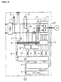
- FIG. 10 is a block diagram showing a configuration of a circuit in a conventional inverter apparatus.
- the inverter apparatus is composed of a converter 1 connected to a two- or three-phase alternate power supply to convert an alternate current into a direct current; an electrolytic capacitor 2 for smoothing; an IPM 3; a control circuit consisting of a central processing unit 6 (CPU-ROM) including a buffer 4, a controller 5, and a memory; a power supply circuit for the IPM 3 and control circuit consisting of a switching transistor 7, transistors 8, 9, and a switching regulator 10; and a current transformer CT installed between an output of the IPM 3 and a motor M.
- CPU-ROM central processing unit 6
- the IPM 3 is integrally composed of a three-phase inverter 11 that is composed of a power element and that provides an output connected to the motor M; a predriver 12 for controlling and driving the inverter 11; a protection circuit 13; a sensor 14 for detecting an overcurrent; a sensor 15 for detecting overheating; a braking power element 16 and a resistor 17 that are used to provide deceleration control for the motor M; and a predriver 18 for controlling and driving the braking power element 16.
- a control signal from the control circuit to the IPM 3 is supplied from the buffer 4 to the predrivers 12, 18 via a photocoupler, and an alarm signal issued when the sensor 14, 15 detects an overcurrent or overheated condition is supplied from the protection circuit 13 to the buffer 4 via the photocoupler.
- an output from the current transformer CT is connected to the controller 5.
- the current transformer CT detects an output current flowing from the IPM 3 to the motor M in order to return this current to the controller 5 for various forms of control.
- the current transformer CT has three through-holes therein, and is provided in the inverter apparatus in such a manner that wires or bars that act as output-current lines from the inverter 11 are inserted through these through-holes.
- a direct voltage converted by the converter 1 is converted by the inverter 11 into an alternate voltage supplied to the motor M.
- bridges are assembled using IGBTs (Insulated Gate Bipolar Transistors) and diodes, and the IGBTs chopping-control a direct current to allow an alternate current to consequently flow through the motor. By varying the frequency of this alternate current, the motor's rotation speed can be varied.
- an inverter output current detected by the current transformer CT is input to the controller 5, which then provides control such that the waveform of the output current will not be distorted or such that the output voltage will not exceed a predetermined value.
- FIG 11 is a block diagram showing a power conversion circuit in a conventional inverter apparatus.
- the power conversion circuit is composed of two modules, that is, the converter 1 and the IPM 3 including the inverter 11.
- Module terminals 21 to 25, which are shown by a circle, are provided for the converter 1 as I/O terminals, and module terminals 26 to 30 are provided for the IPM 3.
- terminal blocks R, S, T, P1, P2, N, U, V, and W which are shown by large black circles, are provided as I/O terminals for the inverter apparatus including the converter 1 and the IPM 3.
- the module terminals 21 to 30 of the converter 1 and IPM 3 are connected to the corresponding terminal blocks, and these connections are carried out by, for example, screwing copper bars to the blocks.
- the connections between the converter 1 and the inverter 11, that is, the connections between the terminal blocks P1 and P2 and between the module terminals 25 and 27 are also carried out by screwing copper bars to the blocks.
- the current transformer built into the conventional inverter apparatus to monitor an output current is relatively larger than the other components and thus requires a large installation space, thereby hindering the development of more compact inverter apparatuses.
- the wires or bars acting as output current lines must be inserted through the current transformer, the number of assembly steps is so large that the process becomes complicated.
- the apparatus since the module terminals and the terminal blocks are connected together by screwing wire rods such as copper bars, the apparatus requires a large number of set screws for connections, a complex wiring pattern, and a large number of assembly steps. In addition, an installation space must be provided for the wiring, and this constitutes a constraint on space-saving efforts.
- the electrical apparatus described in these documents suffers from one or more of the above described problems.
- the present invention has been provided in view of these points. It is intended to provide a semiconductor device that can provide added space for the incorporated devices and that can reduce requirements for both wiring space and the number of assembly steps.
- a semiconductor device comprises a power semiconductor, a drive circuit, and a protection circuit that are integrated into the same package, in which the semiconductor device comprises input-side and output-side module terminals connected to a main circuit of said power semiconductor, and in which the semiconductor device is integrated in use with an apparatus comprising its own terminal blocks, characterized in that at least some of said module terminals are integrated with said terminal blocks of said apparatus.
- the module terminals of the semiconductor device are integrated with the terminal blocks of the apparatus into which this semiconductor device is integrated, thereby eliminating the needs for the wire rods and set screws for connections used to connect the module terminals and terminal blocks. As a result, both the wiring space and the number of assembly steps can be reduced.
- the inverter apparatus shown in Figure 1 has almost the same configuration and effects as the conventional inverter apparatus shown in Figure 10 .
- components used in the conventional inverter apparatus are assigned the same reference numerals and their details are omitted.
- the differences between this inverter apparatus and the conventional inverter apparatus are twofold: first, a shunt resistor 31 is built into the IPM 3 in such a way as to be inserted in series with output lines from the IPM 3; and second, an insulating amplifier 32 or an voltage-resistant IC replacing the insulating amplifier is provided to return a terminal voltage of the shunt resistor 31 to the controller 5.
- the shunt resistor 31 has both ends wired to control pins of the IPM 3 via a pattern.
- the shunt resistor 31 can provide an output current to the controller 5 as a voltage value and monitor an output current flowing through the motor M as in a current transformer.
- the current transformer can be omitted from the inverter to reduce the installation space, the number of wiring steps, and thus the size of the apparatus.
- the shunt resistor 31 can radiate heat efficiently.
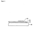
- FIG. 2 shows an example of a configuration of an IPM near a shunt resistor.
- the shunt resistor 31 is composed of an insulating layer 33, an adhesion layer 34, and a resistor 35.
- the shunt resistor 31 is mounted on an insulating substrate 36 together with functional elements constituting the IPM 3, that is, power elements of the inverter 11. Those elements such as the predrivers 12, 18 and a protection circuit that do not require radiation are mounted on a printed circuit board separate from the insulating substrate 36.
- the insulating substrate 36 may comprise a metal insulating substrate, this embodiment uses a ceramic substrate having a copper circuit pattern formed on its surface, with the shunt resistor 31 joined with the substrate via a solder 37.
- the insulating substrate 36 is joined with a copper base 38 via a solder 39.
- the shunt resistor 31 is soldered to the insulating substrate 36 of the IPM 3, and heat generated in the shunt resistor is radiated via the insulating substrate 36 and the copper base 38.
- the shunt resistor 31 built into the IPM 3 improves the latter's radiating capability to enable it to be applied when high-current output of 50 A or more is required.
- FIG 3 shows another example of a configuration of an IPM near a shunt resistor.
- the shunt resistor 31 is configured by directly depositing the resistor 35 onto the insulating substrate 36 joined with the copper base 38 via the solder 39. In this manner, by directly forming the shunt resistor 31 on the insulating substrate 36, the heat resistance between the resistor 35 and the copper base 38 decreases to improve the IPM's radiating capability.
- This configuration can restrain temperature rises in the shunt resistor 31 and improve the inverter's load tolerance.
- the resistor 35 is formed on the insulating substrate 36 by means of deposition, the resistor 35 may be joined with the insulating substrate 36 by means of pressure contact, adhesion, brazing, or an active metal method.
- the shunt resistor 31 has been mounted on the insulating substrate 36 as described above, the IPM 3 on which the shunt resistor 31 is mounted are manufactured so as to have different output currents depending on the specification of the inverter to which the IPM is applied.
- the resistance value of the shunt resistor 31 must be varied depending on the rated output current of the IPM 3. Consequently, a plurality of shunt resistors having different resistance values are provided so that a shunt resistor having an optimal resistance value is used as required. In this case, however, due to the large number of resistance values required, handling of the shunt resistor becomes quite cumbersome, as does stock management.
- the present invention uses only one shunt resistor 31, and adjusts the resistance value by varying the bonding positions of the wire. The details are described below.
- Figure 4 is a top view of the shunt resistor.
- Figure 4(A) shows that bonding positions are evenly arranged and Figure 4(B) shows equipotential lines.
- the shunt resistor 31 is composed of the resistor 35, conductive bonding regions 41, 42 placed on the respective sides of the resistor 35, and conductive sense terminals 43, 44 connected to part of the respective sides of the resistor 35.
- the bonding region 41 is connected via a bonding wire 46 to a circuit pattern 45 on the insulating substrate 36 that corresponds to a current output line of the inverter 11.
- the bonding region 42 is connected via a bonding wire 48 to a circuit pattern 47 on the insulating substrate 36 that corresponds to a current output line leading to an output of the IPM 3.
- the sense terminals 43, 44 are connected to a circuit pattern on the insulating substrate 36 that leads to control pins of the IPM 3, which are connected to the controller 5 via an external device, in this example, the insulating amplifier 32.
- the voltage between the sense terminals 43 and 44 was 250 mV. This indicates the resistance value of the resistor 35 is 2.5 m ⁇ , as seen from between the sense terminals 43 and 44.
- Figure 5 is a top view of the shunt resistor.
- Figure 5(A) shows that the bonding positions are biased to a side opposed to the sense terminals
- Figure 5(B) shows the relevant equipotential lines.
- the bonding positions 49, 50 are closely arranged in the bonding regions 41, 42 away from the sense terminals 43, 44.
- the current density and the current path are concentrated between the bonding positions 49 and 50, and the current density decreases as the distance between these positions increases.
- the equipotential lines in the resistor 35 are distributed in parallel only between the bonding positions, and the interval between the equipotential lines is larger on the side of the resistor closer to the sense terminals 43, 44, as shown in Figure 5(B) .
- Figure 6 is a top view of the shunt resistor.
- Figure 6(A) shows that the bonding positions are biased to the sense terminals
- Figure 6(B) shows the equipotential lines.
- the bonding positions 49, 50 of the bonding wires 46, 48 are closely arranged in the bonding regions 41, 42 near the sense terminals 43, 44, the current density and the current path concentrate between the bonding positions 49 and 50, and the equipotential lines in the resistor 35 are distributed as shown in Figure 6(B) .
- one type of shunt resistor can be used to provide different resistance values, thereby eliminating the need to prepare a shunt resistor of a specific resistance value to meet the specifications of the inverter.
- the module terminals of the IPM 3 and the terminal blocks of the inverter apparatus are integrated together to enable the copper bars and their set screws to be omitted. This configuration is explained below.
- FIG. 7 is a block diagram showing a power conversion circuit in the inverter apparatus.
- the power conversion circuit is composed of the two modules, that is, the converter 1 and the IPM 3.
- the converter 1 comprises the module terminals as its I/O terminals, and of these terminals, the input terminals and positive-pole input terminals are integrated with the alternate-input terminal blocks R, S, T, P1 of the inverter apparatus, thereby eliminating the need for the copper bars and their set screws.
- the module terminals 24, 25 of the converter 1 are connected to an electrolytic capacitor.
- the input-side module terminals are integrated with the direct-input terminal blocks P2, N of the inverter apparatus, and the output-side module terminals are integrated with the terminal blocks U, V, W.
- module terminals P(+)1, P(+)2, N(-)1, N(-)2 are provided in the immediate neighborhood of an IGBT constituting the inverter 11 of the IPM 3.
- These module terminals P(+)1, P(+)2, N(-)1, N(-)2 are connected to a capacitor for a snubber circuit for restraining a surge voltage generated upon a switching operation of the IGBT.
- the input-side module terminals of the IPM 3 are integrated with the terminal blocks P2, N, so the wires between the terminal blocks P2, N and the IGBTs tend to be long, thereby increasing the inductances L1, L2 of the internal wires between the terminal blocks P2, N and the IGBT.
- the inductances L1, L2 of the wires may cause a large surge voltage to be generated upon a switching operation of the IGBT, thus destroying the IGBT.
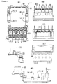
- Figure 8 shows an example of the IPM's appearance.
- Figure 8(A) is a top view
- Figure 8(B) is a front view
- Figure 8(C) is a partial sectional view of the terminal block
- Figure 8(D) is a rear view
- Figure 8(E) is a right-side view.
- the IPM 3 comprises on a frame mounted in an outer circumferential portion of the copper base 38, the inverter apparatus terminal blocks P2, N, U, V, W integrated with the module terminals of the IPM, the module terminals P(+)1, P(+)2, N(-)1, N(-)2 for the snubber circuit, and a connector 51 having control pins connected to an external control circuit.
- Two sets of the terminals blocks P2, N, U, V, W are provided, wherein one set is provided on the top surface of the frame, while the other is provided on the front surface of the frame.
- the IGBT, predrivers 12, 18, protection circuit 13, and shunt resistor 31 formed on the insulating substrate 36 are located at the center of the frame and are sealed by a cover 52.
- the terminal block P2 is connected to the terminal block P1 and electrolytic capacitor of the converter 1, and the terminal blocks U, V, W are connected to the motor M.
- the module terminals P(+)1, P(+)2, N(-)1, N(-)2 for the snubber circuit are separately provided and connected to the circuit pattern located in the immediate neighborhood of the IGBT. Consequently, even if the module terminals and the terminal blocks of the inverter apparatus are integrated together to increase the length of the internal wires 53 between the terminal blocks and the IGBT and thus the inductances of the internal wires 53, the snubber circuit operates in the immediate neighborhood of the IGBT to directly restrain surge voltages generated upon switching. As a result, the presence of any inductance can be substantially neglected to reliably prevent the IGBT from being destroyed by a surge voltage.
- Figure 9 shows another example of the appearance of the IPM.
- Figure 9(A) is a top view
- Figure 9(B) is a front view
- Figure 9(C) is a rear view
- Figure 9(D) is a partial sectional view of the terminal block
- Figure 9(E) is a bottom view of the neighborhood of the terminal block
- Figure 9(E) is a right-side view.
- the IPM 3 comprises the inverter apparatus terminal blocks P2, N, U, V, W integrated with the module terminals of the IPM, the module terminals P(+)1, P(+)2, N(-)1, N(-)2 for the snubber circuit, and the connector 51 having control pins for connection to an external control circuit.
- Two sets of the terminals blocks P2, N, U, V, W are provided on the top side of the frame.
- the IGBT, predrivers 12, 18, protection circuit 13, and shunt resistor 31 formed on the insulating substrate 36 are located at the center of the frame and are sealed by the cover 52.
- the module terminals P(+)1, N(-)1 and P(+)2, N(-)2 are directly connected to the two capacitors for the snubber circuit placed on the cover 52.
- the terminal block P2 is connected to the terminal block P1 and electrolytic capacitor of the converter 1, and the terminal blocks U, V, W are connected to the motor M.
- the module terminals and the terminal blocks of the inverter apparatus are also integrated together via the internal wires 53 to eliminate the needs for copper bars and their mounting screws for wiring.
- the module terminals P(+)1, P(+)2, N(-)1, N(-)2 for the snubber circuit are connected to the circuit pattern located in the immediate neighborhood of the IGBT, the snubber circuit operates in the immediate neighborhood of the IGBT to enable the effects of any inductance for wires between the terminal blocks of the inverter apparatus and the IGBT to be neglected.
- the above described embodiments incorporate a shunt resistor for detecting an output current, both ends of which can be connected to an external device.
- This configuration enables the inverter apparatus to omit the current transformer and thus to reduce requirements for both installation space and the number of wiring steps, and also to enable the output current to be controlled based on the detected voltage, using a connection with the external device.
- the apparatus's radiating capability can be improved by providing the shunt resistor on the insulating substrate with the power elements mounted thereon, so the present invention can be applied to an inverter apparatus designed for high currents of 50 A and.
- a single shunt resistor can be used to realize a plurality of resistance values.
- the present invention in particular provides for the module terminals and the terminal blocks of the inverter apparatus to be integrated together, so internal wiring materials and set screws can be omitted to reduce requirements for both installation space and the number of assembly steps.
- the present invention can eliminate the effects of any wire inductance associated with the longer wire lengths required for integration of the module terminals and the terminal blocks.
Description
- The present invention relates to a semiconductor device and in particular, to a semiconductor device built into an electric conversion apparatus such as a general inverter apparatus, a numerically controlled machine tool, or an air conditioner.
- In general, an inverter apparatus that is applied to a variable-speed gear for a motor is composed of a power element for electric conversions, a drive circuit for controlling and driving the power element, a protection circuit, and a control circuit for generally controlling these components. Semiconductor devices called "intelligent power modules (hereafter referred to as "IPMs") have been commercially available that comprise an integrated package including, of the above components, a power element for converting a direct current into an alternate current, a drive circuit, and a protection circuit.
-
Figure 10 is a block diagram showing a configuration of a circuit in a conventional inverter apparatus. The inverter apparatus is composed of aconverter 1 connected to a two- or three-phase alternate power supply to convert an alternate current into a direct current; anelectrolytic capacitor 2 for smoothing; anIPM 3; a control circuit consisting of a central processing unit 6 (CPU-ROM) including a buffer 4, acontroller 5, and a memory; a power supply circuit for theIPM 3 and control circuit consisting of aswitching transistor 7,transistors 8, 9, and aswitching regulator 10; and a current transformer CT installed between an output of theIPM 3 and a motor M. - The IPM 3 is integrally composed of a three-
phase inverter 11 that is composed of a power element and that provides an output connected to the motor M; apredriver 12 for controlling and driving theinverter 11; aprotection circuit 13; asensor 14 for detecting an overcurrent; asensor 15 for detecting overheating; abraking power element 16 and aresistor 17 that are used to provide deceleration control for the motor M; and apredriver 18 for controlling and driving thebraking power element 16. - A control signal from the control circuit to the
IPM 3 is supplied from the buffer 4 to thepredrivers sensor protection circuit 13 to the buffer 4 via the photocoupler. In addition, an output from the current transformer CT is connected to thecontroller 5. - The current transformer CT detects an output current flowing from the
IPM 3 to the motor M in order to return this current to thecontroller 5 for various forms of control. The current transformer CT has three through-holes therein, and is provided in the inverter apparatus in such a manner that wires or bars that act as output-current lines from theinverter 11 are inserted through these through-holes. - In the inverter apparatus of the configuration described above, a direct voltage converted by the
converter 1 is converted by theinverter 11 into an alternate voltage supplied to the motor M. In theinverter 11, bridges are assembled using IGBTs (Insulated Gate Bipolar Transistors) and diodes, and the IGBTs chopping-control a direct current to allow an alternate current to consequently flow through the motor. By varying the frequency of this alternate current, the motor's rotation speed can be varied. - In addition, an inverter output current detected by the current transformer CT is input to the
controller 5, which then provides control such that the waveform of the output current will not be distorted or such that the output voltage will not exceed a predetermined value. -
Figure 11 is a block diagram showing a power conversion circuit in a conventional inverter apparatus. The power conversion circuit is composed of two modules, that is, theconverter 1 and the IPM 3 including theinverter 11.Module terminals 21 to 25, which are shown by a circle, are provided for theconverter 1 as I/O terminals, andmodule terminals 26 to 30 are provided for theIPM 3. In addition, terminal blocks R, S, T, P1, P2, N, U, V, and W, which are shown by large black circles, are provided as I/O terminals for the inverter apparatus including theconverter 1 and theIPM 3. - The
module terminals 21 to 30 of theconverter 1 andIPM 3 are connected to the corresponding terminal blocks, and these connections are carried out by, for example, screwing copper bars to the blocks. The connections between theconverter 1 and theinverter 11, that is, the connections between the terminal blocks P1 and P2 and between themodule terminals - However, the current transformer built into the conventional inverter apparatus to monitor an output current is relatively larger than the other components and thus requires a large installation space, thereby hindering the development of more compact inverter apparatuses. In addition, since the wires or bars acting as output current lines must be inserted through the current transformer, the number of assembly steps is so large that the process becomes complicated.
- In addition, since the module terminals and the terminal blocks are connected together by screwing wire rods such as copper bars, the apparatus requires a large number of set screws for connections, a complex wiring pattern, and a large number of assembly steps. In addition, an installation space must be provided for the wiring, and this constitutes a constraint on space-saving efforts.
- Generally known apparatus like that described above is disclosed in
WO 98/10508 EP 0664595 MITSUBISHI ELECTRIC CORP and in "Integration of High Frequency Current Shunts In Power Electronic Circuits" by FERREIRA J A Et AL, published in "Proceedings of the Annual Power Electronics Specialists Conference (PESC), Toledo, June 29 - July 3, 1992, New York, IEEE, US, vol. 2 CONF. 23, 29 June 1992 (1992-06-29), pages 1284 - 1290, XP000369143 ISBN: 0-7803-0695-3." - Further apparatus are known from
US 5 543 659 andJP 093 12 376 A - The electrical apparatus described in these documents suffers from one or more of the above described problems. The present invention has been provided in view of these points. It is intended to provide a semiconductor device that can provide added space for the incorporated devices and that can reduce requirements for both wiring space and the number of assembly steps.
- Therefore, according to the present invention a semiconductor device comprises a power semiconductor, a drive circuit, and a protection circuit that are integrated into the same package, in which the semiconductor device comprises input-side and output-side module terminals connected to a main circuit of said power semiconductor, and in which the semiconductor device is integrated in use with an apparatus comprising its own terminal blocks, characterized in that at least some of said module terminals are integrated with said terminal blocks of said apparatus.
- According to such a semiconductor device, the module terminals of the semiconductor device are integrated with the terminal blocks of the apparatus into which this semiconductor device is integrated, thereby eliminating the needs for the wire rods and set screws for connections used to connect the module terminals and terminal blocks. As a result, both the wiring space and the number of assembly steps can be reduced.
- An embodiment of the present invention is described below in detail with reference to the drawings, taking as an example a case in which the invention is applied to an IPM, in which:
-
Figure 1 is a block diagram showing a configuration of a circuit in an inverter apparatus including the IPM to which the present invention has been applied; -
Figure 2 shows an example of a configuration of an IPM near a shunt resistor; -
Figure 3 shows another example of a configuration of the IPM near the shunt resistor; -
Figure 4 is a top view of the shunt resistor, whereFigure 4(A) shows that bonding positions are evenly arranged andFigure 4(B) shows the relevant equipotential lines; -
Figure 5 is a top view of the shunt resistor, whereFigure 5(A) shows that the bonding positions are biased to a side opposed to sense terminals, andFigure 5(B) shows the relevant equipotential lines; -
Figure 6 is a top view of the shunt resistor, whereFigure 6(A) shows that the bonding positions are biased to the sense terminals, andFigure 6(B) shows the relevant equipotential lines; -
Figure 7 is a block diagram showing a power conversion circuit in the inverter apparatus; -
Figure 8 shows an example of the IPM's appearance, whereFigure 8(A) is a top view,Figure 8(B) is a front view,Figure 8(C) is a partial sectional view of a terminal block,Figure 8(D) is a rear view, andFigure 8(E) is a right-side view; -
Figure 9 shows another example of the IPM's appearance, whereFigure 9(A) is a top view,Figure 9(B) is a front view,Figure 9(C) is a rear view,Figure 8(D) is a partial sectional view of a terminal block,Figure 9(E) is a bottom view of the neighborhood of the terminal block, andFigure 9(E) is a right-side view; -
Figure 10 is a block diagram showing a configuration of a circuit in a conventional inverter apparatus; and, -
Figure 11 is a block diagram showing a power conversion circuit in a conventional inverter apparatus. - (The following description of embodiments of inverter apparatus is taken from the parent patent application from which the present patent was divided. It therefore includes reference to various features of the inverter apparatus which do not form a part of the present invention, but of which an understanding is required to fully appreciate the present invention. The essential features of the present invention are described in particular with reference to
Figures 7 ,8 and9 .) - Referring now to the Figures, the inverter apparatus shown in
Figure 1 has almost the same configuration and effects as the conventional inverter apparatus shown inFigure 10 . Thus, components used in the conventional inverter apparatus are assigned the same reference numerals and their details are omitted. The differences between this inverter apparatus and the conventional inverter apparatus are twofold: first, ashunt resistor 31 is built into theIPM 3 in such a way as to be inserted in series with output lines from theIPM 3; and second, aninsulating amplifier 32 or an voltage-resistant IC replacing the insulating amplifier is provided to return a terminal voltage of theshunt resistor 31 to thecontroller 5. - The
shunt resistor 31 has both ends wired to control pins of theIPM 3 via a pattern. Theshunt resistor 31 can provide an output current to thecontroller 5 as a voltage value and monitor an output current flowing through the motor M as in a current transformer. By building theshunt resistor 31 into theIPM 3, the current transformer can be omitted from the inverter to reduce the installation space, the number of wiring steps, and thus the size of the apparatus. In addition, theshunt resistor 31 can radiate heat efficiently. - Next, a configuration of the
shunt resistor 31 for detecting an output current is described. -
Figure 2 shows an example of a configuration of an IPM near a shunt resistor. Theshunt resistor 31 is composed of aninsulating layer 33, anadhesion layer 34, and aresistor 35. Theshunt resistor 31 is mounted on aninsulating substrate 36 together with functional elements constituting theIPM 3, that is, power elements of theinverter 11. Those elements such as thepredrivers insulating substrate 36. Although theinsulating substrate 36 may comprise a metal insulating substrate, this embodiment uses a ceramic substrate having a copper circuit pattern formed on its surface, with theshunt resistor 31 joined with the substrate via asolder 37. Theinsulating substrate 36 is joined with acopper base 38 via asolder 39. - The
shunt resistor 31 is soldered to theinsulating substrate 36 of theIPM 3, and heat generated in the shunt resistor is radiated via theinsulating substrate 36 and thecopper base 38. Theshunt resistor 31 built into theIPM 3 improves the latter's radiating capability to enable it to be applied when high-current output of 50 A or more is required. - Next, another example of a configuration of a shunt resistor that can be applied to an IPM is explained.
-
Figure 3 shows another example of a configuration of an IPM near a shunt resistor. According to this configuration, theshunt resistor 31 is configured by directly depositing theresistor 35 onto theinsulating substrate 36 joined with thecopper base 38 via thesolder 39. In this manner, by directly forming theshunt resistor 31 on the insulatingsubstrate 36, the heat resistance between theresistor 35 and thecopper base 38 decreases to improve the IPM's radiating capability. This configuration can restrain temperature rises in theshunt resistor 31 and improve the inverter's load tolerance. - Although in this example, the
resistor 35 is formed on the insulatingsubstrate 36 by means of deposition, theresistor 35 may be joined with the insulatingsubstrate 36 by means of pressure contact, adhesion, brazing, or an active metal method. - Although the
shunt resistor 31 has been mounted on the insulatingsubstrate 36 as described above, theIPM 3 on which theshunt resistor 31 is mounted are manufactured so as to have different output currents depending on the specification of the inverter to which the IPM is applied. Thus, the resistance value of theshunt resistor 31 must be varied depending on the rated output current of theIPM 3. Consequently, a plurality of shunt resistors having different resistance values are provided so that a shunt resistor having an optimal resistance value is used as required. In this case, however, due to the large number of resistance values required, handling of the shunt resistor becomes quite cumbersome, as does stock management. Thus, the present invention uses only oneshunt resistor 31, and adjusts the resistance value by varying the bonding positions of the wire. The details are described below. -
Figure 4 is a top view of the shunt resistor.Figure 4(A) shows that bonding positions are evenly arranged andFigure 4(B) shows equipotential lines. Theshunt resistor 31 is composed of theresistor 35,conductive bonding regions resistor 35, andconductive sense terminals resistor 35. Thebonding region 41 is connected via abonding wire 46 to acircuit pattern 45 on the insulatingsubstrate 36 that corresponds to a current output line of theinverter 11. Thebonding region 42 is connected via abonding wire 48 to acircuit pattern 47 on the insulatingsubstrate 36 that corresponds to a current output line leading to an output of theIPM 3. By way of example, fivebonding positions 49 are evenly arranged in thebonding region 41, while fivebonding positions 50 are also evenly arranged in thebonding region 42. Although not shown, thesense terminals substrate 36 that leads to control pins of theIPM 3, which are connected to thecontroller 5 via an external device, in this example, the insulatingamplifier 32. - As described above, if the
bonding wires bonding regions resistor 35, and the equipotential lines in theresistor 35 are distributed in parallel as shown inFigure 4(B) . - By way of example, when a 100-A current was allowed to flow through the
shunt resistor 31, the voltage between thesense terminals resistor 35 is 2.5 mΩ, as seen from between thesense terminals -
Figure 5 is a top view of the shunt resistor.Figure 5(A) shows that the bonding positions are biased to a side opposed to the sense terminals, andFigure 5(B) shows the relevant equipotential lines. In this case, the bonding positions 49, 50 are closely arranged in thebonding regions sense terminals resistor 35 are distributed in parallel only between the bonding positions, and the interval between the equipotential lines is larger on the side of the resistor closer to thesense terminals Figure 5(B) . - In this case, when a 100-A current was allowed to flow through the
shunt resistor 31, the potential difference between equipotential lines extending between thesense terminals resistor 35 is 1.81 mΩ, as seen from between thesense terminals -
Figure 6 is a top view of the shunt resistor.Figure 6(A) shows that the bonding positions are biased to the sense terminals, andFigure 6(B) shows the equipotential lines. When the bonding positions 49, 50 of thebonding wires bonding regions sense terminals resistor 35 are distributed as shown inFigure 6(B) . - In this case, when a 100-A current was allowed to flow through the
shunt resistor 31, the potential difference between equipotential lines extending between thesense terminals resistor 35 is 2.9 mΩ, as seen from between thesense terminals sense terminals - Using the characteristic that the resistance value of the
shunt resistor 31 is varied by varying the positions of the wires as described above, one type of shunt resistor can be used to provide different resistance values, thereby eliminating the need to prepare a shunt resistor of a specific resistance value to meet the specifications of the inverter. - In addition, in this inverter apparatus, the module terminals of the
IPM 3 and the terminal blocks of the inverter apparatus are integrated together to enable the copper bars and their set screws to be omitted. This configuration is explained below. -
Figure 7 is a block diagram showing a power conversion circuit in the inverter apparatus. The power conversion circuit is composed of the two modules, that is, theconverter 1 and theIPM 3. Theconverter 1 comprises the module terminals as its I/O terminals, and of these terminals, the input terminals and positive-pole input terminals are integrated with the alternate-input terminal blocks R, S, T, P1 of the inverter apparatus, thereby eliminating the need for the copper bars and their set screws. Themodule terminals converter 1 are connected to an electrolytic capacitor. - Also in the
IPM 3, the input-side module terminals are integrated with the direct-input terminal blocks P2, N of the inverter apparatus, and the output-side module terminals are integrated with the terminal blocks U, V, W. In addition, module terminals P(+)1, P(+)2, N(-)1, N(-)2 are provided in the immediate neighborhood of an IGBT constituting theinverter 11 of theIPM 3. These module terminals P(+)1, P(+)2, N(-)1, N(-)2 are connected to a capacitor for a snubber circuit for restraining a surge voltage generated upon a switching operation of the IGBT. - In this manner, the input-side module terminals of the
IPM 3 are integrated with the terminal blocks P2, N, so the wires between the terminal blocks P2, N and the IGBTs tend to be long, thereby increasing the inductances L1, L2 of the internal wires between the terminal blocks P2, N and the IGBT. In particular, in an inverter apparatus of a medium or large capacity, the inductances L1, L2 of the wires may cause a large surge voltage to be generated upon a switching operation of the IGBT, thus destroying the IGBT. Since, however, the module terminals P(+)1, P(+)2, N(-)1, N(-)2 for the snubber circuit are provided in the immediate neighborhood of the IGBT, the effects of the inductances L1, L2 between the terminal blocks P2, N and the IGBT can be eliminated. -
Figure 8 shows an example of the IPM's appearance.Figure 8(A) is a top view,Figure 8(B) is a front view,Figure 8(C) is a partial sectional view of the terminal block,Figure 8(D) is a rear view, andFigure 8(E) is a right-side view. TheIPM 3 comprises on a frame mounted in an outer circumferential portion of thecopper base 38, the inverter apparatus terminal blocks P2, N, U, V, W integrated with the module terminals of the IPM, the module terminals P(+)1, P(+)2, N(-)1, N(-)2 for the snubber circuit, and aconnector 51 having control pins connected to an external control circuit. Two sets of the terminals blocks P2, N, U, V, W are provided, wherein one set is provided on the top surface of the frame, while the other is provided on the front surface of the frame. The IGBT,predrivers protection circuit 13, and shuntresistor 31 formed on the insulatingsubstrate 36 are located at the center of the frame and are sealed by acover 52. - Two capacitors for the snubber circuit are placed on the
cover 52 and directly connected to the module terminals P(+)1, N(-)1 and P(+)2, N(-)2, respectively. The terminal block P2 is connected to the terminal block P1 and electrolytic capacitor of theconverter 1, and the terminal blocks U, V, W are connected to the motor M. - Those of the module terminals of the
IPM 3 and the terminal blocks of the inverter apparatus that can be shared are integrated together using theinternal wires 53. Consequently, the needs for copper bars and their mounting screws are eliminated, thus helping to substantially reduce both the number of assembly steps and the installation space required for the inverter apparatus. - In addition, the module terminals P(+)1, P(+)2, N(-)1, N(-)2 for the snubber circuit are separately provided and connected to the circuit pattern located in the immediate neighborhood of the IGBT. Consequently, even if the module terminals and the terminal blocks of the inverter apparatus are integrated together to increase the length of the
internal wires 53 between the terminal blocks and the IGBT and thus the inductances of theinternal wires 53, the snubber circuit operates in the immediate neighborhood of the IGBT to directly restrain surge voltages generated upon switching. As a result, the presence of any inductance can be substantially neglected to reliably prevent the IGBT from being destroyed by a surge voltage. -
Figure 9 shows another example of the appearance of the IPM.Figure 9(A) is a top view,Figure 9(B) is a front view,Figure 9(C) is a rear view,Figure 9(D) is a partial sectional view of the terminal block,Figure 9(E) is a bottom view of the neighborhood of the terminal block, andFigure 9(E) is a right-side view. TheIPM 3 comprises the inverter apparatus terminal blocks P2, N, U, V, W integrated with the module terminals of the IPM, the module terminals P(+)1, P(+)2, N(-)1, N(-)2 for the snubber circuit, and theconnector 51 having control pins for connection to an external control circuit. Two sets of the terminals blocks P2, N, U, V, W are provided on the top side of the frame. The IGBT,predrivers protection circuit 13, and shuntresistor 31 formed on the insulatingsubstrate 36 are located at the center of the frame and are sealed by thecover 52. - The module terminals P(+)1, N(-)1 and P(+)2, N(-)2 are directly connected to the two capacitors for the snubber circuit placed on the
cover 52. The terminal block P2 is connected to the terminal block P1 and electrolytic capacitor of theconverter 1, and the terminal blocks U, V, W are connected to the motor M. - In this IPM3, the module terminals and the terminal blocks of the inverter apparatus are also integrated together via the
internal wires 53 to eliminate the needs for copper bars and their mounting screws for wiring. In addition, since the module terminals P(+)1, P(+)2, N(-)1, N(-)2 for the snubber circuit are connected to the circuit pattern located in the immediate neighborhood of the IGBT, the snubber circuit operates in the immediate neighborhood of the IGBT to enable the effects of any inductance for wires between the terminal blocks of the inverter apparatus and the IGBT to be neglected. - Therefore, the above described embodiments incorporate a shunt resistor for detecting an output current, both ends of which can be connected to an external device. This configuration enables the inverter apparatus to omit the current transformer and thus to reduce requirements for both installation space and the number of wiring steps, and also to enable the output current to be controlled based on the detected voltage, using a connection with the external device.
- In addition, the apparatus's radiating capability can be improved by providing the shunt resistor on the insulating substrate with the power elements mounted thereon, so the present invention can be applied to an inverter apparatus designed for high currents of 50 A and.
- In addition, by varying the bonding positions of the wires connected to the shunt resistor to vary the resistance value, a single shunt resistor can be used to realize a plurality of resistance values.
- Furthermore, the present invention in particular provides for the module terminals and the terminal blocks of the inverter apparatus to be integrated together, so internal wiring materials and set screws can be omitted to reduce requirements for both installation space and the number of assembly steps. In addition, since the terminals for the snubber circuits are drawn from the immediate neighborhood of the power elements, the present invention can eliminate the effects of any wire inductance associated with the longer wire lengths required for integration of the module terminals and the terminal blocks.
Claims (3)
- A semiconductor device (3) comprising a power semiconductor (11), a drive circuit (12), and a protection circuit (13) that are integrated into the same package, in which the semiconductor device (3) comprises input-side and output-side module terminals connected to a main circuit of said power semiconductor (11), and in which the semiconductor device (3) is integrated in use with an apparatus comprising its own terminal blocks (N, P1, P2, R, S, T, U, V, W), characterized in that:at least some of said module terminals are integrated with said terminal blocks (P2, N, U, V, W) of said apparatus.
- A semiconductor device (3) according to Claim 1 characterized in that the device (3) comprises an independent terminal (P(+)1, P(+)2, N(-)1 or N(-)2) that is drawn from an immediate neighborhood of said power semiconductor (11) and to which an element for restraining a surge voltage caused by a switching operation of said power semiconductor (11) is connected.
- A semiconductor device (3) according to Claim 2 characterized in that a shunt resistor (31) is provided in series with output lines from said power semiconductor (11) to detect an output current; and in which a terminal voltage of said shunt resistor (31) is output to an external device (5).
Applications Claiming Priority (2)
| Application Number | Priority Date | Filing Date | Title |
|---|---|---|---|
| JP34959798A JP3548024B2 (en) | 1998-12-09 | 1998-12-09 | Semiconductor device and manufacturing method thereof |
| EP99309398A EP1009030B1 (en) | 1998-12-09 | 1999-11-24 | Semiconductor device comprising a power element and a protect circuit |
Related Parent Applications (2)
| Application Number | Title | Priority Date | Filing Date |
|---|---|---|---|
| EP99309398A Division EP1009030B1 (en) | 1998-12-09 | 1999-11-24 | Semiconductor device comprising a power element and a protect circuit |
| EP99309398.8 Division | 1999-11-24 |
Publications (3)
| Publication Number | Publication Date |
|---|---|
| EP2015361A2 EP2015361A2 (en) | 2009-01-14 |
| EP2015361A3 EP2015361A3 (en) | 2009-07-29 |
| EP2015361B1 true EP2015361B1 (en) | 2010-09-29 |
Family
ID=18404813
Family Applications (3)
| Application Number | Title | Priority Date | Filing Date |
|---|---|---|---|
| EP08167294A Expired - Lifetime EP2012357B1 (en) | 1998-12-09 | 1999-11-24 | Method of manufacturing a semi conductor device |
| EP99309398A Expired - Lifetime EP1009030B1 (en) | 1998-12-09 | 1999-11-24 | Semiconductor device comprising a power element and a protect circuit |
| EP08167298A Expired - Lifetime EP2015361B1 (en) | 1998-12-09 | 1999-11-24 | Semi conductor device |
Family Applications Before (2)
| Application Number | Title | Priority Date | Filing Date |
|---|---|---|---|
| EP08167294A Expired - Lifetime EP2012357B1 (en) | 1998-12-09 | 1999-11-24 | Method of manufacturing a semi conductor device |
| EP99309398A Expired - Lifetime EP1009030B1 (en) | 1998-12-09 | 1999-11-24 | Semiconductor device comprising a power element and a protect circuit |
Country Status (4)
| Country | Link |
|---|---|
| US (1) | US6262902B1 (en) |
| EP (3) | EP2012357B1 (en) |
| JP (1) | JP3548024B2 (en) |
| DE (3) | DE69942812D1 (en) |
Families Citing this family (27)
| Publication number | Priority date | Publication date | Assignee | Title |
|---|---|---|---|---|
| JP3826749B2 (en) * | 2001-08-22 | 2006-09-27 | 株式会社日立製作所 | Power converter with shunt resistor |
| DE10143932B4 (en) | 2001-09-07 | 2006-04-27 | eupec Europäische Gesellschaft für Leistungshalbleiter mbH & Co. KG | Shunt resistor assembly |
| WO2003026476A2 (en) * | 2001-09-27 | 2003-04-03 | Galil Medical Ltd. | Apparatus and method for cryosurgical treatment of tumors of the breast |
| JP2003218318A (en) * | 2002-01-21 | 2003-07-31 | Mitsubishi Electric Corp | Semiconductor power module, insulating substrate used for the same and method of manufacturing the same |
| US6653812B1 (en) | 2002-01-31 | 2003-11-25 | Analog Devices, Inc. | Space vector modulation methods and structures for electric-motor control |
| JP4236909B2 (en) * | 2002-11-13 | 2009-03-11 | 三菱電機株式会社 | Power semiconductor module |
| US20040227476A1 (en) * | 2002-12-19 | 2004-11-18 | International Rectifier Corp. | Flexible inverter power module for motor drives |
| JP2004343820A (en) * | 2003-05-13 | 2004-12-02 | Mitsubishi Electric Corp | Power converter |
| KR100669327B1 (en) * | 2004-10-11 | 2007-01-15 | 삼성에스디아이 주식회사 | A plasma display device |
| ES2655254T3 (en) * | 2006-01-16 | 2018-02-19 | Mitsubishi Electric Corporation | Motor control circuit and outdoor unit of air conditioner |
| US7619302B2 (en) * | 2006-05-23 | 2009-11-17 | International Rectifier Corporation | Highly efficient both-side-cooled discrete power package, especially basic element for innovative power modules |
| JP5354144B2 (en) * | 2007-10-22 | 2013-11-27 | 東芝キヤリア株式会社 | Inverter |
| US8482904B2 (en) * | 2010-05-25 | 2013-07-09 | Lear Corporation | Power module with current sensing |
| JP5800192B2 (en) | 2011-10-11 | 2015-10-28 | 富士電機株式会社 | Photocoupler output signal receiving circuit |
| DE102012211924B4 (en) | 2012-07-09 | 2014-02-13 | Infineon Technologies Ag | Semiconductor module having a shunt resistor integrated in a terminal lug and method for detecting a current flowing through a load terminal of a semiconductor module |
| CN102999009B (en) * | 2012-12-11 | 2016-01-20 | 深圳市麦格米特驱动技术有限公司 | Control circuit of machine tool |
| JP5930954B2 (en) * | 2012-12-14 | 2016-06-08 | 三菱電機株式会社 | Power module |
| US9140735B2 (en) | 2013-05-03 | 2015-09-22 | Infineon Technologies Ag | Integration of current measurement in wiring structure of an electronic circuit |
| JPWO2015005181A1 (en) * | 2013-07-08 | 2017-03-02 | 株式会社村田製作所 | Power conversion parts |
| JP2015073261A (en) * | 2013-09-03 | 2015-04-16 | ルネサスエレクトロニクス株式会社 | Semiconductor device |
| JP6487280B2 (en) | 2015-06-11 | 2019-03-20 | ルネサスエレクトロニクス株式会社 | Semiconductor device |
| JP6894181B2 (en) * | 2015-06-17 | 2021-06-30 | ダイキン工業株式会社 | Inverter device |
| CN105609493B (en) * | 2016-03-22 | 2018-05-11 | 富士电机(中国)有限公司 | A kind of eight-in-one IGBT module of integrated bi-directional stepping functions |
| JP6691416B2 (en) * | 2016-04-04 | 2020-04-28 | ダイキン工業株式会社 | Electronic circuit device |
| JP6804646B2 (en) * | 2017-06-22 | 2020-12-23 | 三菱電機株式会社 | Semiconductor module |
| CN109861501A (en) * | 2019-03-25 | 2019-06-07 | 广东美的制冷设备有限公司 | Intelligent power module and air conditioner |
| WO2020191848A1 (en) * | 2019-03-25 | 2020-10-01 | 广东美的制冷设备有限公司 | Integrated controller and control method therefor, and refrigeration device |
Family Cites Families (10)
| Publication number | Priority date | Publication date | Assignee | Title |
|---|---|---|---|---|
| US3676807A (en) * | 1971-05-19 | 1972-07-11 | Tektronix Inc | Film attenuator with distributed capacitance high frequency compensation |
| JPH0231457A (en) * | 1988-07-21 | 1990-02-01 | Matsushita Electric Ind Co Ltd | Light emitting element drive semiconductor device |
| JPH0834705B2 (en) * | 1988-11-16 | 1996-03-29 | 株式会社大林組 | Switch |
| JP2658427B2 (en) * | 1989-01-17 | 1997-09-30 | 富士電機株式会社 | Snubber circuit of semiconductor element for power conversion and its module device |
| US5214407A (en) * | 1991-11-06 | 1993-05-25 | Hewlett-Packard Company | High performance current shunt |
| JP2979930B2 (en) * | 1993-10-28 | 1999-11-22 | 富士電機株式会社 | Power semiconductor device package |
| JP3325697B2 (en) * | 1994-01-20 | 2002-09-17 | 三菱電機株式会社 | Power device control device and motor drive control device |
| JPH09312376A (en) * | 1996-05-21 | 1997-12-02 | Fuji Electric Co Ltd | Semiconductor device |
| EP1028520A1 (en) * | 1996-09-06 | 2000-08-16 | Hitachi, Ltd. | Semiconductor device |
| JP3008924B2 (en) * | 1998-04-10 | 2000-02-14 | 富士電機株式会社 | Power element drive circuit |
-
1998
- 1998-12-09 JP JP34959798A patent/JP3548024B2/en not_active Expired - Lifetime
-
1999
- 1999-11-23 US US09/447,806 patent/US6262902B1/en not_active Expired - Lifetime
- 1999-11-24 EP EP08167294A patent/EP2012357B1/en not_active Expired - Lifetime
- 1999-11-24 DE DE69942812T patent/DE69942812D1/en not_active Expired - Lifetime
- 1999-11-24 DE DE69942796T patent/DE69942796D1/en not_active Expired - Lifetime
- 1999-11-24 DE DE69942813T patent/DE69942813D1/en not_active Expired - Lifetime
- 1999-11-24 EP EP99309398A patent/EP1009030B1/en not_active Expired - Lifetime
- 1999-11-24 EP EP08167298A patent/EP2015361B1/en not_active Expired - Lifetime
Also Published As
| Publication number | Publication date |
|---|---|
| DE69942813D1 (en) | 2010-11-11 |
| EP2012357A3 (en) | 2009-07-29 |
| JP3548024B2 (en) | 2004-07-28 |
| JP2000174202A (en) | 2000-06-23 |
| DE69942796D1 (en) | 2010-11-11 |
| EP2012357A2 (en) | 2009-01-07 |
| DE69942812D1 (en) | 2010-11-11 |
| EP2015361A2 (en) | 2009-01-14 |
| US6262902B1 (en) | 2001-07-17 |
| EP1009030A2 (en) | 2000-06-14 |
| EP1009030B1 (en) | 2010-09-29 |
| EP1009030A3 (en) | 2001-10-17 |
| EP2012357B1 (en) | 2010-09-29 |
| EP2015361A3 (en) | 2009-07-29 |
Similar Documents
| Publication | Publication Date | Title |
|---|---|---|
| EP2015361B1 (en) | Semi conductor device | |
| CN110199388B (en) | High power multilayer module with low inductance and fast switching for parallel power devices | |
| US6373705B1 (en) | Electronic semiconductor module | |
| US6313598B1 (en) | Power semiconductor module and motor drive system | |
| US6215679B1 (en) | Alternator power converter | |
| EP1160866B1 (en) | Semiconductor device with power wiring structure | |
| EP0697732B1 (en) | Driving circuit module | |
| JP3941266B2 (en) | Semiconductor power module | |
| US5896286A (en) | Power semiconductor module | |
| JPH1118429A (en) | Control module | |
| JP4631179B2 (en) | Semiconductor device and inverter device using the same | |
| EP0971412B1 (en) | Power Semiconductor with Attachable Protection Circuit | |
| JP2005252090A (en) | Method for detecting temperature of semiconductor element and semiconductor power converter | |
| JP3747931B2 (en) | Semiconductor device | |
| CN112968622A (en) | Intelligent power module and intelligent power module structure adopting same | |
| JP4246040B2 (en) | Semiconductor device package | |
| EP0527033B1 (en) | Semiconductor module | |
| JPH09135155A (en) | Semiconductor device | |
| GB2305028A (en) | Power module | |
| CN214480328U (en) | Intelligent power module and intelligent power module structure adopting same | |
| WO2024053241A1 (en) | Dc/dc converter and semiconductor device | |
| WO2022097533A1 (en) | Discharge circuit module | |
| JP6983277B2 (en) | Power converter | |
| EP4131760A1 (en) | Highly integrated mosfet half-bridge power module for power converters | |
| JP2001086770A (en) | Main circuit structure of power converter |
Legal Events
| Date | Code | Title | Description |
|---|---|---|---|
| PUAI | Public reference made under article 153(3) epc to a published international application that has entered the european phase |
Free format text: ORIGINAL CODE: 0009012 |
|
| 17P | Request for examination filed |
Effective date: 20081022 |
|
| AC | Divisional application: reference to earlier application |
Ref document number: 1009030 Country of ref document: EP Kind code of ref document: P |
|
| AK | Designated contracting states |
Kind code of ref document: A2 Designated state(s): DE FR GB |
|
| PUAL | Search report despatched |
Free format text: ORIGINAL CODE: 0009013 |
|
| AK | Designated contracting states |
Kind code of ref document: A3 Designated state(s): DE FR GB |
|
| RAP1 | Party data changed (applicant data changed or rights of an application transferred) |
Owner name: FUJI ELECTRIC SYSTEMS CO., LTD. |
|
| AKX | Designation fees paid |
Designated state(s): DE FR GB |
|
| GRAP | Despatch of communication of intention to grant a patent |
Free format text: ORIGINAL CODE: EPIDOSNIGR1 |
|
| GRAS | Grant fee paid |
Free format text: ORIGINAL CODE: EPIDOSNIGR3 |
|
| GRAA | (expected) grant |
Free format text: ORIGINAL CODE: 0009210 |
|
| AC | Divisional application: reference to earlier application |
Ref document number: 1009030 Country of ref document: EP Kind code of ref document: P |
|
| AK | Designated contracting states |
Kind code of ref document: B1 Designated state(s): DE FR GB |
|
| REG | Reference to a national code |
Ref country code: GB Ref legal event code: FG4D |
|
| REF | Corresponds to: |
Ref document number: 69942813 Country of ref document: DE Date of ref document: 20101111 Kind code of ref document: P |
|
| PLBE | No opposition filed within time limit |
Free format text: ORIGINAL CODE: 0009261 |
|
| STAA | Information on the status of an ep patent application or granted ep patent |
Free format text: STATUS: NO OPPOSITION FILED WITHIN TIME LIMIT |
|
| REG | Reference to a national code |
Ref country code: GB Ref legal event code: 732E Free format text: REGISTERED BETWEEN 20110908 AND 20110914 |
|
| REG | Reference to a national code |
Ref country code: DE Ref legal event code: R097 Ref document number: 69942813 Country of ref document: DE Effective date: 20110630 |
|
| REG | Reference to a national code |
Ref country code: FR Ref legal event code: TP Owner name: FUJI ELECTRIC CO., LTD., JP Effective date: 20111021 |
|
| REG | Reference to a national code |
Ref country code: GB Ref legal event code: 746 Effective date: 20121221 |
|
| REG | Reference to a national code |
Ref country code: DE Ref legal event code: R084 Ref document number: 69942813 Country of ref document: DE Effective date: 20121219 |
|
| PGFP | Annual fee paid to national office [announced via postgrant information from national office to epo] |
Ref country code: GB Payment date: 20141119 Year of fee payment: 16 |
|
| REG | Reference to a national code |
Ref country code: FR Ref legal event code: PLFP Year of fee payment: 17 |
|
| PGFP | Annual fee paid to national office [announced via postgrant information from national office to epo] |
Ref country code: FR Payment date: 20151008 Year of fee payment: 17 |
|
| GBPC | Gb: european patent ceased through non-payment of renewal fee |
Effective date: 20151124 |
|
| PG25 | Lapsed in a contracting state [announced via postgrant information from national office to epo] |
Ref country code: GB Free format text: LAPSE BECAUSE OF NON-PAYMENT OF DUE FEES Effective date: 20151124 |
|
| REG | Reference to a national code |
Ref country code: FR Ref legal event code: ST Effective date: 20170731 |
|
| PG25 | Lapsed in a contracting state [announced via postgrant information from national office to epo] |
Ref country code: FR Free format text: LAPSE BECAUSE OF NON-PAYMENT OF DUE FEES Effective date: 20161130 |
|
| PGFP | Annual fee paid to national office [announced via postgrant information from national office to epo] |
Ref country code: DE Payment date: 20171121 Year of fee payment: 19 |
|
| REG | Reference to a national code |
Ref country code: DE Ref legal event code: R119 Ref document number: 69942813 Country of ref document: DE |
|
| PG25 | Lapsed in a contracting state [announced via postgrant information from national office to epo] |
Ref country code: DE Free format text: LAPSE BECAUSE OF NON-PAYMENT OF DUE FEES Effective date: 20190601 |