US6373705B1 - Electronic semiconductor module - Google Patents
Electronic semiconductor module Download PDFInfo
- Publication number
- US6373705B1 US6373705B1 US09/623,971 US62397101A US6373705B1 US 6373705 B1 US6373705 B1 US 6373705B1 US 62397101 A US62397101 A US 62397101A US 6373705 B1 US6373705 B1 US 6373705B1
- Authority
- US
- United States
- Prior art keywords
- semiconductor module
- cooling body
- metal
- insulating layer
- module according
- Prior art date
- Legal status (The legal status is an assumption and is not a legal conclusion. Google has not performed a legal analysis and makes no representation as to the accuracy of the status listed.)
- Expired - Fee Related
Links
Images


Classifications
-
- H—ELECTRICITY
- H01—ELECTRIC ELEMENTS
- H01L—SEMICONDUCTOR DEVICES NOT COVERED BY CLASS H10
- H01L25/00—Assemblies consisting of a plurality of individual semiconductor or other solid state devices ; Multistep manufacturing processes thereof
-
- H—ELECTRICITY
- H01—ELECTRIC ELEMENTS
- H01L—SEMICONDUCTOR DEVICES NOT COVERED BY CLASS H10
- H01L24/00—Arrangements for connecting or disconnecting semiconductor or solid-state bodies; Methods or apparatus related thereto
- H01L24/01—Means for bonding being attached to, or being formed on, the surface to be connected, e.g. chip-to-package, die-attach, "first-level" interconnects; Manufacturing methods related thereto
- H01L24/42—Wire connectors; Manufacturing methods related thereto
- H01L24/47—Structure, shape, material or disposition of the wire connectors after the connecting process
- H01L24/48—Structure, shape, material or disposition of the wire connectors after the connecting process of an individual wire connector
-
- H—ELECTRICITY
- H01—ELECTRIC ELEMENTS
- H01L—SEMICONDUCTOR DEVICES NOT COVERED BY CLASS H10
- H01L23/00—Details of semiconductor or other solid state devices
- H01L23/34—Arrangements for cooling, heating, ventilating or temperature compensation ; Temperature sensing arrangements
- H01L23/36—Selection of materials, or shaping, to facilitate cooling or heating, e.g. heatsinks
-
- H—ELECTRICITY
- H01—ELECTRIC ELEMENTS
- H01L—SEMICONDUCTOR DEVICES NOT COVERED BY CLASS H10
- H01L23/00—Details of semiconductor or other solid state devices
- H01L23/58—Structural electrical arrangements for semiconductor devices not otherwise provided for, e.g. in combination with batteries
- H01L23/64—Impedance arrangements
- H01L23/645—Inductive arrangements
-
- H—ELECTRICITY
- H01—ELECTRIC ELEMENTS
- H01L—SEMICONDUCTOR DEVICES NOT COVERED BY CLASS H10
- H01L2224/00—Indexing scheme for arrangements for connecting or disconnecting semiconductor or solid-state bodies and methods related thereto as covered by H01L24/00
- H01L2224/01—Means for bonding being attached to, or being formed on, the surface to be connected, e.g. chip-to-package, die-attach, "first-level" interconnects; Manufacturing methods related thereto
- H01L2224/02—Bonding areas; Manufacturing methods related thereto
- H01L2224/04—Structure, shape, material or disposition of the bonding areas prior to the connecting process
- H01L2224/05—Structure, shape, material or disposition of the bonding areas prior to the connecting process of an individual bonding area
- H01L2224/0554—External layer
- H01L2224/05599—Material
-
- H—ELECTRICITY
- H01—ELECTRIC ELEMENTS
- H01L—SEMICONDUCTOR DEVICES NOT COVERED BY CLASS H10
- H01L2224/00—Indexing scheme for arrangements for connecting or disconnecting semiconductor or solid-state bodies and methods related thereto as covered by H01L24/00
- H01L2224/01—Means for bonding being attached to, or being formed on, the surface to be connected, e.g. chip-to-package, die-attach, "first-level" interconnects; Manufacturing methods related thereto
- H01L2224/42—Wire connectors; Manufacturing methods related thereto
- H01L2224/47—Structure, shape, material or disposition of the wire connectors after the connecting process
- H01L2224/48—Structure, shape, material or disposition of the wire connectors after the connecting process of an individual wire connector
- H01L2224/4805—Shape
- H01L2224/4809—Loop shape
- H01L2224/48091—Arched
-
- H—ELECTRICITY
- H01—ELECTRIC ELEMENTS
- H01L—SEMICONDUCTOR DEVICES NOT COVERED BY CLASS H10
- H01L2224/00—Indexing scheme for arrangements for connecting or disconnecting semiconductor or solid-state bodies and methods related thereto as covered by H01L24/00
- H01L2224/01—Means for bonding being attached to, or being formed on, the surface to be connected, e.g. chip-to-package, die-attach, "first-level" interconnects; Manufacturing methods related thereto
- H01L2224/42—Wire connectors; Manufacturing methods related thereto
- H01L2224/47—Structure, shape, material or disposition of the wire connectors after the connecting process
- H01L2224/48—Structure, shape, material or disposition of the wire connectors after the connecting process of an individual wire connector
- H01L2224/481—Disposition
- H01L2224/48151—Connecting between a semiconductor or solid-state body and an item not being a semiconductor or solid-state body, e.g. chip-to-substrate, chip-to-passive
- H01L2224/48221—Connecting between a semiconductor or solid-state body and an item not being a semiconductor or solid-state body, e.g. chip-to-substrate, chip-to-passive the body and the item being stacked
- H01L2224/48225—Connecting between a semiconductor or solid-state body and an item not being a semiconductor or solid-state body, e.g. chip-to-substrate, chip-to-passive the body and the item being stacked the item being non-metallic, e.g. insulating substrate with or without metallisation
- H01L2224/48227—Connecting between a semiconductor or solid-state body and an item not being a semiconductor or solid-state body, e.g. chip-to-substrate, chip-to-passive the body and the item being stacked the item being non-metallic, e.g. insulating substrate with or without metallisation connecting the wire to a bond pad of the item
- H01L2224/48228—Connecting between a semiconductor or solid-state body and an item not being a semiconductor or solid-state body, e.g. chip-to-substrate, chip-to-passive the body and the item being stacked the item being non-metallic, e.g. insulating substrate with or without metallisation connecting the wire to a bond pad of the item the bond pad being disposed in a recess of the surface of the item
-
- H—ELECTRICITY
- H01—ELECTRIC ELEMENTS
- H01L—SEMICONDUCTOR DEVICES NOT COVERED BY CLASS H10
- H01L2224/00—Indexing scheme for arrangements for connecting or disconnecting semiconductor or solid-state bodies and methods related thereto as covered by H01L24/00
- H01L2224/01—Means for bonding being attached to, or being formed on, the surface to be connected, e.g. chip-to-package, die-attach, "first-level" interconnects; Manufacturing methods related thereto
- H01L2224/42—Wire connectors; Manufacturing methods related thereto
- H01L2224/47—Structure, shape, material or disposition of the wire connectors after the connecting process
- H01L2224/48—Structure, shape, material or disposition of the wire connectors after the connecting process of an individual wire connector
- H01L2224/484—Connecting portions
-
- H—ELECTRICITY
- H01—ELECTRIC ELEMENTS
- H01L—SEMICONDUCTOR DEVICES NOT COVERED BY CLASS H10
- H01L2224/00—Indexing scheme for arrangements for connecting or disconnecting semiconductor or solid-state bodies and methods related thereto as covered by H01L24/00
- H01L2224/80—Methods for connecting semiconductor or other solid state bodies using means for bonding being attached to, or being formed on, the surface to be connected
- H01L2224/85—Methods for connecting semiconductor or other solid state bodies using means for bonding being attached to, or being formed on, the surface to be connected using a wire connector
- H01L2224/8538—Bonding interfaces outside the semiconductor or solid-state body
- H01L2224/85399—Material
-
- H—ELECTRICITY
- H01—ELECTRIC ELEMENTS
- H01L—SEMICONDUCTOR DEVICES NOT COVERED BY CLASS H10
- H01L2924/00—Indexing scheme for arrangements or methods for connecting or disconnecting semiconductor or solid-state bodies as covered by H01L24/00
- H01L2924/0001—Technical content checked by a classifier
- H01L2924/00014—Technical content checked by a classifier the subject-matter covered by the group, the symbol of which is combined with the symbol of this group, being disclosed without further technical details
-
- H—ELECTRICITY
- H01—ELECTRIC ELEMENTS
- H01L—SEMICONDUCTOR DEVICES NOT COVERED BY CLASS H10
- H01L2924/00—Indexing scheme for arrangements or methods for connecting or disconnecting semiconductor or solid-state bodies as covered by H01L24/00
- H01L2924/01—Chemical elements
- H01L2924/01005—Boron [B]
-
- H—ELECTRICITY
- H01—ELECTRIC ELEMENTS
- H01L—SEMICONDUCTOR DEVICES NOT COVERED BY CLASS H10
- H01L2924/00—Indexing scheme for arrangements or methods for connecting or disconnecting semiconductor or solid-state bodies as covered by H01L24/00
- H01L2924/01—Chemical elements
- H01L2924/01006—Carbon [C]
-
- H—ELECTRICITY
- H01—ELECTRIC ELEMENTS
- H01L—SEMICONDUCTOR DEVICES NOT COVERED BY CLASS H10
- H01L2924/00—Indexing scheme for arrangements or methods for connecting or disconnecting semiconductor or solid-state bodies as covered by H01L24/00
- H01L2924/01—Chemical elements
- H01L2924/01011—Sodium [Na]
-
- H—ELECTRICITY
- H01—ELECTRIC ELEMENTS
- H01L—SEMICONDUCTOR DEVICES NOT COVERED BY CLASS H10
- H01L2924/00—Indexing scheme for arrangements or methods for connecting or disconnecting semiconductor or solid-state bodies as covered by H01L24/00
- H01L2924/01—Chemical elements
- H01L2924/01013—Aluminum [Al]
-
- H—ELECTRICITY
- H01—ELECTRIC ELEMENTS
- H01L—SEMICONDUCTOR DEVICES NOT COVERED BY CLASS H10
- H01L2924/00—Indexing scheme for arrangements or methods for connecting or disconnecting semiconductor or solid-state bodies as covered by H01L24/00
- H01L2924/01—Chemical elements
- H01L2924/01015—Phosphorus [P]
-
- H—ELECTRICITY
- H01—ELECTRIC ELEMENTS
- H01L—SEMICONDUCTOR DEVICES NOT COVERED BY CLASS H10
- H01L2924/00—Indexing scheme for arrangements or methods for connecting or disconnecting semiconductor or solid-state bodies as covered by H01L24/00
- H01L2924/01—Chemical elements
- H01L2924/01029—Copper [Cu]
-
- H—ELECTRICITY
- H01—ELECTRIC ELEMENTS
- H01L—SEMICONDUCTOR DEVICES NOT COVERED BY CLASS H10
- H01L2924/00—Indexing scheme for arrangements or methods for connecting or disconnecting semiconductor or solid-state bodies as covered by H01L24/00
- H01L2924/01—Chemical elements
- H01L2924/01052—Tellurium [Te]
-
- H—ELECTRICITY
- H01—ELECTRIC ELEMENTS
- H01L—SEMICONDUCTOR DEVICES NOT COVERED BY CLASS H10
- H01L2924/00—Indexing scheme for arrangements or methods for connecting or disconnecting semiconductor or solid-state bodies as covered by H01L24/00
- H01L2924/013—Alloys
- H01L2924/014—Solder alloys
-
- H—ELECTRICITY
- H01—ELECTRIC ELEMENTS
- H01L—SEMICONDUCTOR DEVICES NOT COVERED BY CLASS H10
- H01L2924/00—Indexing scheme for arrangements or methods for connecting or disconnecting semiconductor or solid-state bodies as covered by H01L24/00
- H01L2924/10—Details of semiconductor or other solid state devices to be connected
- H01L2924/11—Device type
- H01L2924/13—Discrete devices, e.g. 3 terminal devices
- H01L2924/1304—Transistor
- H01L2924/1305—Bipolar Junction Transistor [BJT]
- H01L2924/13055—Insulated gate bipolar transistor [IGBT]
-
- H—ELECTRICITY
- H01—ELECTRIC ELEMENTS
- H01L—SEMICONDUCTOR DEVICES NOT COVERED BY CLASS H10
- H01L2924/00—Indexing scheme for arrangements or methods for connecting or disconnecting semiconductor or solid-state bodies as covered by H01L24/00
- H01L2924/10—Details of semiconductor or other solid state devices to be connected
- H01L2924/11—Device type
- H01L2924/13—Discrete devices, e.g. 3 terminal devices
- H01L2924/1304—Transistor
- H01L2924/1306—Field-effect transistor [FET]
- H01L2924/13091—Metal-Oxide-Semiconductor Field-Effect Transistor [MOSFET]
-
- H—ELECTRICITY
- H01—ELECTRIC ELEMENTS
- H01L—SEMICONDUCTOR DEVICES NOT COVERED BY CLASS H10
- H01L2924/00—Indexing scheme for arrangements or methods for connecting or disconnecting semiconductor or solid-state bodies as covered by H01L24/00
- H01L2924/19—Details of hybrid assemblies other than the semiconductor or other solid state devices to be connected
- H01L2924/1901—Structure
- H01L2924/1904—Component type
- H01L2924/19041—Component type being a capacitor
-
- H—ELECTRICITY
- H01—ELECTRIC ELEMENTS
- H01L—SEMICONDUCTOR DEVICES NOT COVERED BY CLASS H10
- H01L2924/00—Indexing scheme for arrangements or methods for connecting or disconnecting semiconductor or solid-state bodies as covered by H01L24/00
- H01L2924/19—Details of hybrid assemblies other than the semiconductor or other solid state devices to be connected
- H01L2924/191—Disposition
- H01L2924/19101—Disposition of discrete passive components
- H01L2924/19107—Disposition of discrete passive components off-chip wires
-
- H—ELECTRICITY
- H01—ELECTRIC ELEMENTS
- H01L—SEMICONDUCTOR DEVICES NOT COVERED BY CLASS H10
- H01L2924/00—Indexing scheme for arrangements or methods for connecting or disconnecting semiconductor or solid-state bodies as covered by H01L24/00
- H01L2924/30—Technical effects
- H01L2924/301—Electrical effects
- H01L2924/30107—Inductance
Definitions
- the present invention relates to an electronic semiconductor module.
- IMS insulated metal substrate
- the carrier substrate includes a metal plate which functions as a cooling body and has an electrically insulating layer on its upper side and a thin metal layer arranged on the insulating layer.
- the insulating layer conducts heat effectively and includes, for example, a thin polymer layer into which ceramic powder is introduced to improve its ability to dissipate heat.
- Printed conductors are formed on the upper side of the substrate by structuring the metal layer.
- Electronic semiconductor components are provided on the upper side and electrically connected to the printed conductors via bonding wires.
- the direct copper bonded substrates include a relatively thick ceramic carrier, with its upper and lower side being provided with a thin metal layer via a special compression process.
- Printed conductors are provided on the upper metal layer via structuring.
- semiconductor components are connected to the printed conductors via bonding wires.
- a thick metal plate which functions as a heat sink is soldered onto the lower metal layer of the carrier substrate.
- cooling channels through which a cooling medium flows can be provided in the metal plate.
- a particular disadvantage of the direct copper bonded substrates compared with the insulated metal substrates is that the ceramic layer is thick, which makes it more difficult for heat to be transmitted to the cooling body.
- the known semiconductor modules described above have the following disadvantage that all the terminal connectors of the semiconductor components are arranged on the upper side of the carrier substrate. Because the printed conductors paths are all in this one position, they are very complicated. In electronic circuits with a high level of integration, the substrate, which is in any case expensive, must be enlarged laterally to house all the necessary printed conductor wiring on the upper side of the carrier substrate. This considerably increases manufacturing costs. It is particularly disadvantageous that because all the terminal connectors are arranged in the upper metal layer of the substrate, significant parasitic inductivity arises and can cause substantial overvoltages. This has a particularly disadvantageous impact if power electronic circuits having direct voltage circuits are arranged on the carrier substrate.
- the parasitic inductivity causes undesirable overvoltages which have to be taken into account when selecting the semiconductor components.
- the switch-off procedure of an electronic circuit breaker has to be slowed via suitable measures so as to reduce overvoltages and prevent damage to the semiconductor module.
- the known problems can be avoided via the semiconductor module according to the present invention. It is advantageous that the heat generated by the semiconductor components can be dissipated effectively, and at the same time the parasitic inductivity of the semiconductor module can be significantly reduced.
- An insulated metal substrate is used as the carrier substrate of the semiconductor module, the insulating intermediate layer of the insulated metal substrate having at least one notch, and at least one terminal face of a semiconductor component provided on the upper side of the semiconductor component facing away from the carrier substrate being electrically connected to a contact element which is directly connected to the metal cooling body via the notch. Because the cooling body is used as an electrical conductor that is directly electrically connected to the terminal of a semiconductor component via the contact element, it is possible to significantly reduce the parasitic inductivity of the semiconductor module.
- the metal cooling body also functions as a conductor for conveying the power required to operate the semiconductor component. Thanks to the very thin electrically insulating layer, and respectively, the very thin dielectric between the cooling body and the printed conductors on the upper side of the substrate, the parasitic inductivity is reduced further, and at the same time heat is dissipated into the cooling body very quickly and efficiently.
- the contact element can be manufactured as a bonding wire which at one end is connected to the terminal of the semiconductor component and at the other end to the metal cooling body.
- Bonding wire technology is well understood and thanks to the direct connection between the bonding wire and the cooling body it is only necessary to create small notches in the insulating intermediate layer; these can be created inexpensively using a laser.
- the metal cooling body is provided as a potential surface for making available the supply potential, in particular the ground potential, required to operate the semiconductor component.
- the insulating layer is less than 250 ⁇ m thick.
- Heat can be dissipated particularly efficiently if the metal cooling body is coupled with a cooling medium. It is particularly advantageous if the metal cooling body of the insulated metal substrate has cooling channels through which the cooling medium flows.
- FIG. 1 shows a semiconductor module that is known from the related art.
- FIG. 2 shows a first exemplary embodiment of a semiconductor module according to the present invention.
- FIG. 3 shows a second exemplary embodiment of a semiconductor module according to the present invention.
- FIG. 4 shows a circuit diagram for the semiconductor module of a step-down converter shown in FIGS. 1, 2 , and 3 .
- FIG. 1 shows a semiconductor module that is known from the related art.
- a direct copper bonded substrate is used as carrier substrate 1 and includes an approximately 1-millimeter-thick ceramic layer 2 , on the upper and lower sides of which approximately 300 ⁇ m-thick copper metal layers 4 , 5 have been applied.
- insulated metal substrates having a thin insulating layer provided with a metal layer on its upper side and a metal cooling body arranged directly on its lower side can be used.
- Printed conductors 4 a , 4 b , 4 c are formed in upper metal layer 4 via structuring.
- Non-housed semiconductor components 20 , 21 for example MOSFETs, power diodes, IGBTs or bipolar transistors, are provided on metal layer 4 .
- Terminals (not shown) on the lower side of semiconductor components 20 , 21 are electrically connected to printed conductors 4 a , 4 c , for example by soldering on non-housed semiconductor elements 20 , 21 .
- the semiconductor components are electrically connected to further printed conductors 4 b , 4 c via bonding wires 11 , 14 , which are connected to terminal faces 22 , 23 on the upper side of the semiconductor components.
- a metal cooling body 3 which is made of, for example, copper, is soldered onto metal layer 5 on the lower side of carrier substrate 1 .
- the lower side of cooling body 3 is in contact with a cooling medium 10 , which is, for example, a cooling fluid.
- Further electrical components, such as a capacitor 30 are connected to printed conductors 4 a , 4 b via conductive connectors 40 , 41 and metal jumpers 42 , 43 .
- FIG. 4 A circuit diagram of the step-down converter is shown in FIG. 4, the electrical and electronic components of the semiconductor module being shown inside dot-dash line 50 .
- Terminal B+ of the operating potential is connected to printed conductor 4 a in FIG. 1; terminal B ⁇ is connected to printed conductor 4 b .
- Phase terminal P is connected to printed conductor 4 c .
- semiconductor component 21 is a circuit breaker, e.g., a MOSFET, and component 20 is a semiconductor diode. If circuit breaker 21 is switched off, the current commutates from MOSFET 21 to diode 20 . The following is true of electrical voltage U MOSFET that drops at the MOSFET when switching off:
- U MOSFET U 1 (L 1 +L 2 +L 4 +L 5 +L 6 +L 7 ). dI 1 /dt and dI 1 /dt ⁇ 0,
- U 1 being the intermediate circuit voltage applied to the semiconductor module between printed conductors 4 a and 4 b and L 1 to L 7 being the parasitic inductivities that arise.
- the greater the parasitic inductivities L 1 to L 7 the greater the undesirable overvoltage.
- the parasitic inductivities shown in FIG. 4 can be assigned directly to the structure of the semiconductor module in FIG. 1 . In FIG.
- parasitic inductivity L 1 is caused by electrical terminal connector 40 of positive pole 32 of intermediate circuit capacitor 30 .
- Parasitic inductivity L 2 is caused by terminal link 43 and printed conductor 4 a .
- Parasitic inductivities L 3 and L 5 are caused by the electrical conductive connector from MOSFET 21 to semiconductor diode 20 , i.e., by bonding wire 11 and printed conductor 4 c .
- Parasitic inductivity L 6 is caused by printed conductor 4 b and terminal link 42 ; parasitic inductivity L 7 is caused by terminal connector 41 of intermediate circuit capacitor 30 .
- Parasitic inductivity L 4 relating to the connection from the contact designated P to printed conductor 4 c is not shown in FIG. 1 .
- Inductivities L 2 and L 7 can be slightly reduced thanks to the fact that terminal connectors 40 and 41 are arranged close to one another in intermediate circuit bar 45 ; however, as FIG. 1 indicates, there is a large area between the B+ terminal and the B ⁇ terminal of the semiconductor module, i.e., between terminal links 43 and 42 , which means parasitic inductivities L 2 and L 6 are substantial and cannot be significantly reduced by optimizing the structure.
- the connection between printed conductor 4 c and semiconductor component 20 is more problematic, because potential terminals B+ and B ⁇ are arranged in upper metal layer 4 , which means parasitic inductivities L 3 and L 5 are substantial.
- parasitic inductivities L 1 to L 7 cannot be reduced further, which results in the disadvantages described above.
- FIG. 2 shows a first exemplary embodiment of the semiconductor module according to the present invention.
- the advantages will be explained with reference to a step-down converter.
- the advantages apply in the case of any bonding or isolating power electronic circuits having a direct voltage circuit.
- an insulated metal substrate which is known per se and which includes a metal cooling body 3 , which is a plurality of millimeters thick and is made of, for example, aluminum, and on the upper side of which an electrically insulating layer 2 is applied, is used as carrier substrate 1 for the semiconductor module.
- the electrically insulating layer is 140 ⁇ m thick and should not be thicker than 250 ⁇ m thick.
- the insulating layer is preferably made of a polymer into which ceramic particles that conduct heat effectively have been introduced.
- An approximately 300- ⁇ m-thick metal layer 4 in which printed conductors 4 a , 4 c are formed via structuring in a known manner and which is made of, for example, copper is applied to insulating layer 2 .
- the lower side of metal cooling body 3 is in heat contact with a cooling medium 10 .
- Non-housed semiconductor components 20 , 21 are arranged on metal layer 4 .
- semiconductor component 21 is a MOSFET and semiconductor component 20 is a semiconductor diode.
- an IGBT, bipolar transistor or other semiconductor component can be used instead of the MOSFET.
- a switchable power semiconductor for example a bipolar transistor, MOSFET or IGBT, can be used instead of the semiconductor diode.
- the lower side of MOSFET 21 is in electrical contact with printed conductor 4 a .
- Two terminal faces 23 are arranged on the upper side of MOSFET 21 facing away from carrier substrate 1 ; in FIG. 2, just one is shown. Terminal face 23 is connected to a bonding wire 11 whose end is connected to printed conductor 4 c .
- On the lower side of semiconductor diode 20 there is a first terminal face which is electrically connected to printed conductor 4 c .
- a second terminal face 22 of semiconductor diode 20 is arranged on the side of the semiconductor diode facing away from carrier substrate 1 and is connected to a contact element embodied as bonding wire 12 .
- Bonding wire 12 is electrically connected directly to cooling body 3 via the gap between printed conductors 4 c and 4 a . and via a notch 13 in insulating layer 2 .
- a direct connection means a connection without intermediate connections involving other components.
- Notch 13 has a diameter of, for example, 3 millimeters and can be created in insulating 2 easily using a laser. In contrast with a direct copper bonded substrate, the stability of carrier substrate 1 is guaranteed thanks to metal plate 3 and thus is not diminished by notch 13 in insulating layer 2 .
- positive pole 32 of an intermediate circuit a capacitor 30 is connected to printed conductor 4 a on the upper side of carrier substrate 1 via a recess 33 provided in cooling body 3 and insulating layer 2 , for example via screwing or riveting.
- Negative pole 31 of intermediate circuit capacitor 30 is connected to cooling body 3 .
- supply potential B+ is connected to printed conductor 4 a and ground potential B ⁇ is connected to cooling body 3 .
- one terminal of the power semiconductor components is often connected to ground potential so that cooling body 3 can be connected to the B ⁇ potential directly without an insulating intermediate layer.
- cooling body 3 As a conductor for conveying ground potential B ⁇ , the area between potentials B+ and B ⁇ can be significantly reduced compared to that in the known semiconductor modules shown in FIG. 1 and thus parasitic inductivities L 2 and L 6 can be reduced substantially.
- Upper metal layer 4 largely conveys just potential B+. Only the area for printed conductor 4 c and the gap between the printed conductors have to be created.
- parasitic inductivities L 1 and L 7 can be reduced much more significantly than with the intermediate circuit bar of the semiconductor module shown in FIG. 1 .
- the semiconductor module according to the present invention it is advantageous that the heat generated by semiconductor components 20 , 21 passes very quickly through insulating layer 2 , which is thin and conducts heat effectively, to cooling body 3 and from there is transferred into cooling medium 10 .
- cooling body 3 can form the joint ground terminal for all the components. This makes it much easier to create the printed conductor paths on the upper side of the substrate.
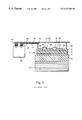
- FIG. 3 shows a further exemplary embodiment of the semiconductor module according to the present invention. Elements that are the same have been assigned the same reference numbers.
- cooling body 3 has meandering cooling channels 15 through which cooling medium 10 flows. As a result, the heat is dissipated even more effectively.
- the use of the semiconductor module according to the present invention is not by any means limited to the application described above, namely a step-down converter; indeed the semiconductor module can also be used to reduce parasitic inductivity and improve heat dissipation in other power electronic circuit topologies having a direct voltage circuit.
Landscapes
- Engineering & Computer Science (AREA)
- Microelectronics & Electronic Packaging (AREA)
- Computer Hardware Design (AREA)
- Power Engineering (AREA)
- Physics & Mathematics (AREA)
- Condensed Matter Physics & Semiconductors (AREA)
- General Physics & Mathematics (AREA)
- Chemical & Material Sciences (AREA)
- Materials Engineering (AREA)
- Cooling Or The Like Of Semiconductors Or Solid State Devices (AREA)
Abstract
Description
Claims (8)
Applications Claiming Priority (3)
| Application Number | Priority Date | Filing Date | Title |
|---|---|---|---|
| DE19900603 | 1999-01-11 | ||
| DE19900603A DE19900603A1 (en) | 1999-01-11 | 1999-01-11 | Electronic semiconductor module |
| PCT/DE1999/004085 WO2000042654A1 (en) | 1999-01-11 | 1999-12-23 | Electronic semiconductor module |
Publications (1)
| Publication Number | Publication Date |
|---|---|
| US6373705B1 true US6373705B1 (en) | 2002-04-16 |
Family
ID=7893876
Family Applications (1)
| Application Number | Title | Priority Date | Filing Date |
|---|---|---|---|
| US09/623,971 Expired - Fee Related US6373705B1 (en) | 1999-01-11 | 1999-12-23 | Electronic semiconductor module |
Country Status (6)
| Country | Link |
|---|---|
| US (1) | US6373705B1 (en) |
| EP (1) | EP1062698A1 (en) |
| JP (1) | JP2002535835A (en) |
| KR (1) | KR100695031B1 (en) |
| DE (1) | DE19900603A1 (en) |
| WO (1) | WO2000042654A1 (en) |
Cited By (36)
| Publication number | Priority date | Publication date | Assignee | Title |
|---|---|---|---|---|
| US20020186545A1 (en) * | 2000-05-25 | 2002-12-12 | Mitsubishi Denki Kabushiki Kaisha | Power module |
| US6522544B1 (en) * | 2000-05-16 | 2003-02-18 | Mitsubishi Denki Kabushiki Kaisha | Power module |
| EP1434268A2 (en) * | 2002-12-26 | 2004-06-30 | Yamaha Hatsudoki Kabushiki Kaisha | Electronic substrate, power module and motor driver |
| US6760225B1 (en) * | 2003-01-20 | 2004-07-06 | Power Mate Technology Co., Ltd. | Heat-dissipating structure of circuit board |
| US20040180581A1 (en) * | 2001-11-07 | 2004-09-16 | Radi Medical Systems Ab | Bending resistant male connector for a guide wire |
| US20040200829A1 (en) * | 2003-04-12 | 2004-10-14 | Andreas Hamburger | Device for receiving ceramic heating elements and method for the manufacture thereof |
| US20040251533A1 (en) * | 2003-06-11 | 2004-12-16 | Takeshi Suzuki | Hybrid integrated circuit device |
| US20050161781A1 (en) * | 2003-12-24 | 2005-07-28 | Sanyo Electric Co., Ltd. | Hybrid integrated circuit device and manufacturing method thereof |
| US7042745B1 (en) * | 2004-11-29 | 2006-05-09 | Cotek Electronic Ind. Co. Ltd. | Insulating arrangement for DC/AC inverter |
| US20060250205A1 (en) * | 2005-05-04 | 2006-11-09 | Honeywell International Inc. | Thermally conductive element for cooling an air gap inductor, air gap inductor including same and method of cooling an air gap inductor |
| US20070114665A1 (en) * | 2004-04-16 | 2007-05-24 | Reinhold Bayerer | Power Semiconductor Circuit |
| EP1968188A1 (en) * | 2007-03-09 | 2008-09-10 | HÜTTINGER Elektronik GmbH + Co. KG | Class D amplifier assembly |
| US20080266805A1 (en) * | 2004-12-01 | 2008-10-30 | Electrische Apparatenfabriek Capax B.V. | Carrier For Electrical Components With Soldered-On Cooling Body |
| US20090026194A1 (en) * | 2007-07-18 | 2009-01-29 | Catem Gmbh & Co. Kg | Method of Manufacturing an Electric Heating Device and Electric Heating Devices |
| US20090086436A1 (en) * | 2006-03-23 | 2009-04-02 | Claus Peter Kluge | Carrier body for components or circuits |
| US20090289354A1 (en) * | 2008-05-20 | 2009-11-26 | Infineon Technologies Ag | Electronic module |
| US20090293857A1 (en) * | 2005-06-29 | 2009-12-03 | Bsh Bosch Und Siemens Hausgerate Gmbh | Domestic Appliance and a Cookable Product Holding Device Therefor |
| WO2010050896A1 (en) * | 2008-10-29 | 2010-05-06 | Opulent Electronics International Pte Ltd | Insulated metal substrate and method of forming the same |
| US20100172091A1 (en) * | 2008-11-28 | 2010-07-08 | Fuji Electric Systems Co., Ltd. | Cooling apparatus for semiconductor chips |
| US20100226093A1 (en) * | 2009-03-09 | 2010-09-09 | General Electric Company | Methods for making millichannel substrate, and cooling device and apparatus using the substrate |
| US20110049535A1 (en) * | 2008-05-08 | 2011-03-03 | Toyota Jidosha Kabushiki Kaisha | Semiconductor apparatus |
| US20130056862A1 (en) * | 2011-09-07 | 2013-03-07 | Stats Chippac, Ltd. | Semiconductor Device and Method of Forming a Low Profile Dual-Purpose Shield and Heat-Dissipation Structure |
| US8837150B2 (en) | 2009-09-15 | 2014-09-16 | Lisa Dräxlmaier GmbH | Electronic device for switching currents and method for producing the same |
| US20140293554A1 (en) * | 2011-02-08 | 2014-10-02 | Cambridge Nanotherm Limited | Insulated metal substrate |
| US20140313673A1 (en) * | 2013-04-22 | 2014-10-23 | Mitsubishi Electric Corporation | Electronic device |
| CN104396011A (en) * | 2012-07-04 | 2015-03-04 | 松下知识产权经营株式会社 | Semiconductor device |
| US20170011985A1 (en) * | 2015-07-10 | 2017-01-12 | Semikron Elektronik Gmbh & Co., Kg | Power electronics module with load connection elements |
| CN106876352A (en) * | 2017-03-27 | 2017-06-20 | 广东美的制冷设备有限公司 | SPM, the preparation method of SPM and power electronic equipment |
| US20170288654A1 (en) * | 2016-04-04 | 2017-10-05 | Infineon Technologies Austria Ag | Half Bridge Circuit, Method of Operating a Half Bridge Circuit and a Half Bridge Circuit Package |
| US20190225054A1 (en) * | 2018-01-23 | 2019-07-25 | Borgwarner Ludwigsburg Gmbh | Heating device and method for producing a heating rod |
| US20200022279A1 (en) * | 2016-09-22 | 2020-01-16 | Robert Bosch Gmbh | Electronic module, in particular an electronic power module for hybrid vehicles or electric vehicles |
| US10930458B2 (en) * | 2016-09-09 | 2021-02-23 | Eaton Intelligent Power Limited | Low-voltage circuit breaker |
| US11111137B2 (en) | 2016-08-29 | 2021-09-07 | Robert Bosch Gmbh | Method for manufacturing a micromechanical sensor |
| US20210407880A1 (en) * | 2020-06-30 | 2021-12-30 | Zf Friedrichshafen Ag | Power module for operating an electric vehicle drive with improved temperature determination of the power semiconductors |
| US20220344286A1 (en) * | 2021-04-23 | 2022-10-27 | Denso Corporation | Semiconductor module |
| US11497112B2 (en) | 2020-12-11 | 2022-11-08 | Toyota Motor Engineering & Manufacturing North America, Inc. | Driver board assemblies and methods of forming a driver board assembly |
Families Citing this family (14)
| Publication number | Priority date | Publication date | Assignee | Title |
|---|---|---|---|---|
| DE10114572A1 (en) | 2001-03-24 | 2002-11-07 | Marquardt Gmbh | Carrier for an electrical circuit, in particular for an electrical switch |
| DE10257100B4 (en) * | 2002-07-12 | 2008-08-14 | Danfoss Silicon Power Gmbh | breakers |
| DE10239512A1 (en) | 2002-08-28 | 2004-03-11 | Minebea Co. Ltd., A Japanese Corporation | Power/control application structure for direct current electric motor e.g. in motor vehicles, has first and second printed circuit boards with control/power electronic parts and an electrically insulated substrate to dissipate heat |
| JP4751810B2 (en) * | 2006-11-02 | 2011-08-17 | 日立オートモティブシステムズ株式会社 | Power converter |
| JP4968150B2 (en) * | 2008-04-07 | 2012-07-04 | 株式会社豊田自動織機 | Semiconductor element cooling device |
| DE102010002950A1 (en) * | 2010-03-17 | 2011-09-22 | Robert Bosch Gmbh | CIRCUIT ARRANGEMENT AND ASSOCIATED CONTROL UNIT FOR A MOTOR VEHICLE |
| DE102012202765B3 (en) * | 2012-02-23 | 2013-04-18 | Semikron Elektronik Gmbh & Co. Kg | Semiconductor module |
| DE102015203587A1 (en) * | 2015-02-27 | 2016-09-01 | Siemens Aktiengesellschaft | Method of manufacturing a power electronic system with integrated heat exchanger and power electronic system |
| EP3340293A1 (en) * | 2016-12-20 | 2018-06-27 | Siemens Aktiengesellschaft | Semiconductor module with support structure on the bottom |
| EP3748835A1 (en) | 2019-06-06 | 2020-12-09 | Infineon Technologies AG | Power semiconductor module arrangement |
| DE102020103844A1 (en) | 2020-02-14 | 2021-08-19 | Bayerische Motoren Werke Aktiengesellschaft | Cooling device for a semiconductor switch of an electronic switching device, electrical arrangement and method |
| DE102020210296A1 (en) | 2020-08-13 | 2022-02-17 | Robert Bosch Gesellschaft mit beschränkter Haftung | Switching device, electrical energy storage and device |
| DE102020213972B4 (en) | 2020-11-06 | 2022-10-13 | Robert Bosch Gesellschaft mit beschränkter Haftung | Power module with a split heat sink |
| DE102022207429A1 (en) | 2022-07-21 | 2024-02-01 | Zf Friedrichshafen Ag | Cooling device for a power converter for a vehicle, power converter, electric axle drive, vehicle and method for producing a cooling device |
Citations (9)
| Publication number | Priority date | Publication date | Assignee | Title |
|---|---|---|---|---|
| EP0018174A1 (en) | 1979-04-12 | 1980-10-29 | Fujitsu Limited | High frequency semiconductor device on an insulating substrate |
| US4777060A (en) | 1986-09-17 | 1988-10-11 | Schwarzkopf Development Corporation | Method for making a composite substrate for electronic semiconductor parts |
| EP0508717A1 (en) | 1991-04-08 | 1992-10-14 | General Electric Company | Integrated heat sink for semiconductor modules |
| US5398160A (en) * | 1992-10-20 | 1995-03-14 | Fujitsu General Limited | Compact power module with a heat spreader |
| US5436793A (en) * | 1993-03-31 | 1995-07-25 | Ncr Corporation | Apparatus for containing and cooling an integrated circuit device having a thermally insulative positioning member |
| US5504378A (en) * | 1994-06-10 | 1996-04-02 | Westinghouse Electric Corp. | Direct cooled switching module for electric vehicle propulsion system |
| US5763951A (en) * | 1996-07-22 | 1998-06-09 | Northrop Grumman Corporation | Non-mechanical magnetic pump for liquid cooling |
| US6060772A (en) * | 1997-06-30 | 2000-05-09 | Kabushiki Kaisha Toshiba | Power semiconductor module with a plurality of semiconductor chips |
| US6295201B1 (en) * | 1998-08-04 | 2001-09-25 | Stratos Lightwave, Inc. | Bus bar having embedded switching device |
Family Cites Families (2)
| Publication number | Priority date | Publication date | Assignee | Title |
|---|---|---|---|---|
| JPH0521668A (en) * | 1991-07-16 | 1993-01-29 | Sumitomo Electric Ind Ltd | Semiconductor device substrate |
| JPH1022552A (en) * | 1996-07-04 | 1998-01-23 | Mitsubishi Electric Corp | Solid laser device and its light source |
-
1999
- 1999-01-11 DE DE19900603A patent/DE19900603A1/en not_active Ceased
- 1999-12-23 KR KR1020007009911A patent/KR100695031B1/en not_active IP Right Cessation
- 1999-12-23 WO PCT/DE1999/004085 patent/WO2000042654A1/en active IP Right Grant
- 1999-12-23 JP JP2000594153A patent/JP2002535835A/en active Pending
- 1999-12-23 EP EP99967900A patent/EP1062698A1/en not_active Ceased
- 1999-12-23 US US09/623,971 patent/US6373705B1/en not_active Expired - Fee Related
Patent Citations (9)
| Publication number | Priority date | Publication date | Assignee | Title |
|---|---|---|---|---|
| EP0018174A1 (en) | 1979-04-12 | 1980-10-29 | Fujitsu Limited | High frequency semiconductor device on an insulating substrate |
| US4777060A (en) | 1986-09-17 | 1988-10-11 | Schwarzkopf Development Corporation | Method for making a composite substrate for electronic semiconductor parts |
| EP0508717A1 (en) | 1991-04-08 | 1992-10-14 | General Electric Company | Integrated heat sink for semiconductor modules |
| US5398160A (en) * | 1992-10-20 | 1995-03-14 | Fujitsu General Limited | Compact power module with a heat spreader |
| US5436793A (en) * | 1993-03-31 | 1995-07-25 | Ncr Corporation | Apparatus for containing and cooling an integrated circuit device having a thermally insulative positioning member |
| US5504378A (en) * | 1994-06-10 | 1996-04-02 | Westinghouse Electric Corp. | Direct cooled switching module for electric vehicle propulsion system |
| US5763951A (en) * | 1996-07-22 | 1998-06-09 | Northrop Grumman Corporation | Non-mechanical magnetic pump for liquid cooling |
| US6060772A (en) * | 1997-06-30 | 2000-05-09 | Kabushiki Kaisha Toshiba | Power semiconductor module with a plurality of semiconductor chips |
| US6295201B1 (en) * | 1998-08-04 | 2001-09-25 | Stratos Lightwave, Inc. | Bus bar having embedded switching device |
Non-Patent Citations (2)
| Title |
|---|
| ** H. de Lambilly, H. Kesser "Failure Analysis of Power Modules: A Look at the Packaging and Reliability of Large IGBTs", (1992), pp. 366-370, IEEE/CHMT Int. Electronics Manufacturing Technology Symposium. |
| *Research Disclosure, GB, Industrial Opportunities Ltd. Havant, "Use of a Composite Metal Pad for Wire Bond Connection to the Coppercore of a Metal Core Substrate Circuit Board", Sep. 1, 1989, p. 683. |
Cited By (78)
| Publication number | Priority date | Publication date | Assignee | Title |
|---|---|---|---|---|
| US20040179341A1 (en) * | 2000-05-16 | 2004-09-16 | Mitsubishi Denki Kabushiki Kaisha | Power module |
| US6522544B1 (en) * | 2000-05-16 | 2003-02-18 | Mitsubishi Denki Kabushiki Kaisha | Power module |
| US6900986B2 (en) | 2000-05-16 | 2005-05-31 | Mitsubishi Denki Kabushiki Kaisha | Power module |
| US20020186545A1 (en) * | 2000-05-25 | 2002-12-12 | Mitsubishi Denki Kabushiki Kaisha | Power module |
| US7081671B2 (en) | 2000-05-25 | 2006-07-25 | Mitsubishi Denki Kabushiki Kaisha | Power module |
| US20100273358A1 (en) * | 2001-11-07 | 2010-10-28 | Radi Medical Systems Ab | Bending resistant male connector for a guide wire |
| US20040180581A1 (en) * | 2001-11-07 | 2004-09-16 | Radi Medical Systems Ab | Bending resistant male connector for a guide wire |
| US8323215B2 (en) | 2001-11-07 | 2012-12-04 | Radi Medical Systems Ab | Bending resistant male connector for a guide wire |
| US8109889B2 (en) | 2001-11-07 | 2012-02-07 | Radi Medical Systems Ab | Bending resistant male connector for a guide wire |
| US6908442B2 (en) * | 2001-11-07 | 2005-06-21 | Radi Medical Systems Ab | Bending resistant male connector for a guide wire |
| US20050186848A1 (en) * | 2001-11-07 | 2005-08-25 | Radi Medical Systems Ab | Bending resistant male connector for a guide wire |
| US7775992B2 (en) | 2001-11-07 | 2010-08-17 | Radi Medical Systems Ab | Bending resistant male connector for a guide wire |
| US20050087849A1 (en) * | 2002-12-26 | 2005-04-28 | Yamaha Hatsudoki Kabushiki Kaisha | Electronic substrate, power module and motor driver |
| EP1434268A3 (en) * | 2002-12-26 | 2004-08-25 | Yamaha Hatsudoki Kabushiki Kaisha | Electronic substrate, power module and motor driver |
| EP1434268A2 (en) * | 2002-12-26 | 2004-06-30 | Yamaha Hatsudoki Kabushiki Kaisha | Electronic substrate, power module and motor driver |
| CN100390971C (en) * | 2002-12-26 | 2008-05-28 | 雅马哈发动机株式会社 | Electronic substrate, power module, and motor driver |
| US7119437B2 (en) | 2002-12-26 | 2006-10-10 | Yamaha Hatsudoki Kabushiki Kaisha | Electronic substrate, power module and motor driver |
| US6760225B1 (en) * | 2003-01-20 | 2004-07-06 | Power Mate Technology Co., Ltd. | Heat-dissipating structure of circuit board |
| US7816630B2 (en) | 2003-04-12 | 2010-10-19 | Eichenauer Heizelemente Gmbh & Co. Kg | Device for receiving ceramic heating elements and method for the manufacture thereof |
| US20060138712A1 (en) * | 2003-04-12 | 2006-06-29 | Andreas Hamburger | Device for receiving ceramic heating elements and method for the manufacture thereof |
| US7977610B2 (en) * | 2003-04-12 | 2011-07-12 | Borgwarner Beru Systems Gmbh | Device for receiving ceramic heating elements and method for the manufacture thereof |
| US20040200829A1 (en) * | 2003-04-12 | 2004-10-14 | Andreas Hamburger | Device for receiving ceramic heating elements and method for the manufacture thereof |
| US20040251533A1 (en) * | 2003-06-11 | 2004-12-16 | Takeshi Suzuki | Hybrid integrated circuit device |
| CN100336425C (en) * | 2003-06-11 | 2007-09-05 | 三洋电机株式会社 | Hybrid integrated circuit device |
| US7078797B2 (en) * | 2003-06-11 | 2006-07-18 | Sanyo Electric Co., Ltd. | Hybrid integrated circuit device |
| US20050161781A1 (en) * | 2003-12-24 | 2005-07-28 | Sanyo Electric Co., Ltd. | Hybrid integrated circuit device and manufacturing method thereof |
| US20070114665A1 (en) * | 2004-04-16 | 2007-05-24 | Reinhold Bayerer | Power Semiconductor Circuit |
| US7800213B2 (en) * | 2004-04-16 | 2010-09-21 | Infineon Technologies Ag | Power semiconductor circuit with busbar system |
| US20060114704A1 (en) * | 2004-11-29 | 2006-06-01 | Wei-Kuang Chen | Insulating arrangement for dc/ac inverter |
| US7042745B1 (en) * | 2004-11-29 | 2006-05-09 | Cotek Electronic Ind. Co. Ltd. | Insulating arrangement for DC/AC inverter |
| US20080266805A1 (en) * | 2004-12-01 | 2008-10-30 | Electrische Apparatenfabriek Capax B.V. | Carrier For Electrical Components With Soldered-On Cooling Body |
| US20060250205A1 (en) * | 2005-05-04 | 2006-11-09 | Honeywell International Inc. | Thermally conductive element for cooling an air gap inductor, air gap inductor including same and method of cooling an air gap inductor |
| US20090293857A1 (en) * | 2005-06-29 | 2009-12-03 | Bsh Bosch Und Siemens Hausgerate Gmbh | Domestic Appliance and a Cookable Product Holding Device Therefor |
| CN105590901A (en) * | 2006-03-23 | 2016-05-18 | 陶瓷技术有限责任公司 | Carrier body for components or circuits |
| AU2007228752B2 (en) * | 2006-03-23 | 2012-09-20 | Ceramtec Gmbh | Carrier body for components or circuits |
| US20090086436A1 (en) * | 2006-03-23 | 2009-04-02 | Claus Peter Kluge | Carrier body for components or circuits |
| TWI449137B (en) * | 2006-03-23 | 2014-08-11 | Ceramtec Ag | Traegerkoerper fuer bauelemente oder schaltungen |
| US8040676B2 (en) * | 2006-03-23 | 2011-10-18 | Ceramtec Gmbh | Carrier body for components or circuits |
| EP1968188A1 (en) * | 2007-03-09 | 2008-09-10 | HÜTTINGER Elektronik GmbH + Co. KG | Class D amplifier assembly |
| US7705676B2 (en) | 2007-03-09 | 2010-04-27 | Huettinger Elektronik Gmbh + Co. Kg | Class D amplifier arrangement |
| US20080218264A1 (en) * | 2007-03-09 | 2008-09-11 | Huettinger Gmbh + Co. Kg | Class d amplifier arrangement |
| US8362406B2 (en) * | 2007-07-18 | 2013-01-29 | Catem Gmbh & Co. Kg | Method of manufacturing an electric heating device and electric heating devices |
| US20090026194A1 (en) * | 2007-07-18 | 2009-01-29 | Catem Gmbh & Co. Kg | Method of Manufacturing an Electric Heating Device and Electric Heating Devices |
| US8384211B2 (en) * | 2008-05-08 | 2013-02-26 | Toyota Jidosha Kabushiki Kaisha | Semiconductor apparatus with improved efficiency of thermal radiation |
| US20110049535A1 (en) * | 2008-05-08 | 2011-03-03 | Toyota Jidosha Kabushiki Kaisha | Semiconductor apparatus |
| US8253241B2 (en) | 2008-05-20 | 2012-08-28 | Infineon Technologies Ag | Electronic module |
| US20090289354A1 (en) * | 2008-05-20 | 2009-11-26 | Infineon Technologies Ag | Electronic module |
| US8836113B2 (en) | 2008-05-20 | 2014-09-16 | Infineon Technologies Ag | Electronic module |
| WO2010050896A1 (en) * | 2008-10-29 | 2010-05-06 | Opulent Electronics International Pte Ltd | Insulated metal substrate and method of forming the same |
| US8081465B2 (en) * | 2008-11-28 | 2011-12-20 | Fuji Electric Systems Co., Ltd. | Cooling apparatus for semiconductor chips |
| US20100172091A1 (en) * | 2008-11-28 | 2010-07-08 | Fuji Electric Systems Co., Ltd. | Cooling apparatus for semiconductor chips |
| US7898807B2 (en) * | 2009-03-09 | 2011-03-01 | General Electric Company | Methods for making millichannel substrate, and cooling device and apparatus using the substrate |
| US20100226093A1 (en) * | 2009-03-09 | 2010-09-09 | General Electric Company | Methods for making millichannel substrate, and cooling device and apparatus using the substrate |
| US8837150B2 (en) | 2009-09-15 | 2014-09-16 | Lisa Dräxlmaier GmbH | Electronic device for switching currents and method for producing the same |
| US9551082B2 (en) * | 2011-02-08 | 2017-01-24 | Cambridge Nanotherm Limited | Insulated metal substrate |
| US20140293554A1 (en) * | 2011-02-08 | 2014-10-02 | Cambridge Nanotherm Limited | Insulated metal substrate |
| US9677187B2 (en) | 2011-02-08 | 2017-06-13 | Cambridge Nanolitic Limited | Non-metallic coating and method of its production |
| US20130056862A1 (en) * | 2011-09-07 | 2013-03-07 | Stats Chippac, Ltd. | Semiconductor Device and Method of Forming a Low Profile Dual-Purpose Shield and Heat-Dissipation Structure |
| US10163744B2 (en) * | 2011-09-07 | 2018-12-25 | STATS ChipPAC Pte. Ltd. | Semiconductor device and method of forming a low profile dual-purpose shield and heat-dissipation structure |
| CN104396011A (en) * | 2012-07-04 | 2015-03-04 | 松下知识产权经营株式会社 | Semiconductor device |
| US9379049B2 (en) * | 2012-07-04 | 2016-06-28 | Panasonic Intellectual Property Management Co., Ltd. | Semiconductor apparatus |
| CN104396011B (en) * | 2012-07-04 | 2017-06-06 | 松下知识产权经营株式会社 | Semiconductor device |
| US20150194372A1 (en) * | 2012-07-04 | 2015-07-09 | Panasonic Intellectual Property Management Co., Ltd. | Semiconductor apparatus |
| US9686890B2 (en) * | 2013-04-22 | 2017-06-20 | Mitsubishi Electric Corporation | Electronic device |
| US20140313673A1 (en) * | 2013-04-22 | 2014-10-23 | Mitsubishi Electric Corporation | Electronic device |
| US20170011985A1 (en) * | 2015-07-10 | 2017-01-12 | Semikron Elektronik Gmbh & Co., Kg | Power electronics module with load connection elements |
| US9768094B2 (en) * | 2015-07-10 | 2017-09-19 | Semikron Elektronik Gmbh & Co., Kg | Power electronics module with load connection elements |
| US20170288654A1 (en) * | 2016-04-04 | 2017-10-05 | Infineon Technologies Austria Ag | Half Bridge Circuit, Method of Operating a Half Bridge Circuit and a Half Bridge Circuit Package |
| US10224912B2 (en) * | 2016-04-04 | 2019-03-05 | Infineon Technologies Austria Ag | Half bridge circuit, method of operating a half bridge circuit and a half bridge circuit package |
| US11111137B2 (en) | 2016-08-29 | 2021-09-07 | Robert Bosch Gmbh | Method for manufacturing a micromechanical sensor |
| US10930458B2 (en) * | 2016-09-09 | 2021-02-23 | Eaton Intelligent Power Limited | Low-voltage circuit breaker |
| US20200022279A1 (en) * | 2016-09-22 | 2020-01-16 | Robert Bosch Gmbh | Electronic module, in particular an electronic power module for hybrid vehicles or electric vehicles |
| US11051432B2 (en) * | 2016-09-22 | 2021-06-29 | Robert Bosch Gmbh | Electronic module, in particular an electronic power module for hybrid vehicles or electric vehicles |
| CN106876352A (en) * | 2017-03-27 | 2017-06-20 | 广东美的制冷设备有限公司 | SPM, the preparation method of SPM and power electronic equipment |
| US20190225054A1 (en) * | 2018-01-23 | 2019-07-25 | Borgwarner Ludwigsburg Gmbh | Heating device and method for producing a heating rod |
| US20210407880A1 (en) * | 2020-06-30 | 2021-12-30 | Zf Friedrichshafen Ag | Power module for operating an electric vehicle drive with improved temperature determination of the power semiconductors |
| US11497112B2 (en) | 2020-12-11 | 2022-11-08 | Toyota Motor Engineering & Manufacturing North America, Inc. | Driver board assemblies and methods of forming a driver board assembly |
| US20220344286A1 (en) * | 2021-04-23 | 2022-10-27 | Denso Corporation | Semiconductor module |
Also Published As
| Publication number | Publication date |
|---|---|
| DE19900603A1 (en) | 2000-07-13 |
| EP1062698A1 (en) | 2000-12-27 |
| JP2002535835A (en) | 2002-10-22 |
| WO2000042654A1 (en) | 2000-07-20 |
| KR20010041692A (en) | 2001-05-25 |
| KR100695031B1 (en) | 2007-03-14 |
Similar Documents
| Publication | Publication Date | Title |
|---|---|---|
| US6373705B1 (en) | Electronic semiconductor module | |
| US7045884B2 (en) | Semiconductor device package | |
| US11532538B2 (en) | Component structure, power module and power module assembly structure | |
| US8987777B2 (en) | Stacked half-bridge power module | |
| US6166464A (en) | Power module | |
| US8115294B2 (en) | Multichip module with improved system carrier | |
| JP6354845B2 (en) | Semiconductor module | |
| US8514579B2 (en) | Power semiconductor module including substrates spaced from each other | |
| US7149088B2 (en) | Half-bridge power module with insert molded heatsinks | |
| CN107403773B (en) | Power module, method of manufacturing the same, inverter, and vehicle drive system | |
| US9159715B2 (en) | Miniaturized semiconductor device | |
| JP2023538212A (en) | Power module with at least three power units | |
| US20160255714A1 (en) | Power converter | |
| US10755999B2 (en) | Multi-package top-side-cooling | |
| US11817794B2 (en) | Electronic circuit module | |
| CN110880488B (en) | Semiconductor device and power conversion device | |
| US10356926B1 (en) | Electronic assembly with enhanced high power density | |
| WO2013105456A1 (en) | Circuit board and electronic device | |
| US11973064B2 (en) | Semiconductor power module | |
| US11527456B2 (en) | Power module with organic layers | |
| US6930373B2 (en) | Circuit arrangement | |
| US20240297148A1 (en) | Power module with improved semiconductor die arrangement for active clamping | |
| WO2024033118A1 (en) | Power-module | |
| JP2001217389A (en) | Low-reactance power circuit mounting structure |
Legal Events
| Date | Code | Title | Description |
|---|---|---|---|
| AS | Assignment |
Owner name: ROBERT BOSCH GMBH, GERMANY Free format text: ASSIGNMENT OF ASSIGNORS INTEREST;ASSIGNORS:KOELLE, GERHARD;JACOB, WOLFGANG;TSCHENTSCHER, HARALD;AND OTHERS;REEL/FRAME:011565/0403;SIGNING DATES FROM 20001026 TO 20001123 |
|
| FEPP | Fee payment procedure |
Free format text: PAYOR NUMBER ASSIGNED (ORIGINAL EVENT CODE: ASPN); ENTITY STATUS OF PATENT OWNER: LARGE ENTITY |
|
| FPAY | Fee payment |
Year of fee payment: 4 |
|
| FPAY | Fee payment |
Year of fee payment: 8 |
|
| REMI | Maintenance fee reminder mailed | ||
| LAPS | Lapse for failure to pay maintenance fees | ||
| STCH | Information on status: patent discontinuation |
Free format text: PATENT EXPIRED DUE TO NONPAYMENT OF MAINTENANCE FEES UNDER 37 CFR 1.362 |
|
| FP | Lapsed due to failure to pay maintenance fee |
Effective date: 20140416 |