EP2015135B1 - Elektrochemische Vorrichtung - Google Patents
Elektrochemische Vorrichtung Download PDFInfo
- Publication number
- EP2015135B1 EP2015135B1 EP08167926A EP08167926A EP2015135B1 EP 2015135 B1 EP2015135 B1 EP 2015135B1 EP 08167926 A EP08167926 A EP 08167926A EP 08167926 A EP08167926 A EP 08167926A EP 2015135 B1 EP2015135 B1 EP 2015135B1
- Authority
- EP
- European Patent Office
- Prior art keywords
- electrochromic
- pedot
- pss
- layer
- electrochemically active
- Prior art date
- Legal status (The legal status is an assumption and is not a legal conclusion. Google has not performed a legal analysis and makes no representation as to the accuracy of the status listed.)
- Expired - Lifetime
Links
Images


Classifications
-
- G—PHYSICS
- G02—OPTICS
- G02F—OPTICAL DEVICES OR ARRANGEMENTS FOR THE CONTROL OF LIGHT BY MODIFICATION OF THE OPTICAL PROPERTIES OF THE MEDIA OF THE ELEMENTS INVOLVED THEREIN; NON-LINEAR OPTICS; FREQUENCY-CHANGING OF LIGHT; OPTICAL LOGIC ELEMENTS; OPTICAL ANALOGUE/DIGITAL CONVERTERS
- G02F1/00—Devices or arrangements for the control of the intensity, colour, phase, polarisation or direction of light arriving from an independent light source, e.g. switching, gating or modulating; Non-linear optics
- G02F1/01—Devices or arrangements for the control of the intensity, colour, phase, polarisation or direction of light arriving from an independent light source, e.g. switching, gating or modulating; Non-linear optics for the control of the intensity, phase, polarisation or colour
- G02F1/15—Devices or arrangements for the control of the intensity, colour, phase, polarisation or direction of light arriving from an independent light source, e.g. switching, gating or modulating; Non-linear optics for the control of the intensity, phase, polarisation or colour based on an electrochromic effect
- G02F1/153—Constructional details
- G02F1/155—Electrodes
-
- C—CHEMISTRY; METALLURGY
- C09—DYES; PAINTS; POLISHES; NATURAL RESINS; ADHESIVES; COMPOSITIONS NOT OTHERWISE PROVIDED FOR; APPLICATIONS OF MATERIALS NOT OTHERWISE PROVIDED FOR
- C09K—MATERIALS FOR MISCELLANEOUS APPLICATIONS, NOT PROVIDED FOR ELSEWHERE
- C09K9/00—Tenebrescent materials, i.e. materials for which the range of wavelengths for energy absorption is changed as a result of excitation by some form of energy
- C09K9/02—Organic tenebrescent materials
-
- G—PHYSICS
- G02—OPTICS
- G02F—OPTICAL DEVICES OR ARRANGEMENTS FOR THE CONTROL OF LIGHT BY MODIFICATION OF THE OPTICAL PROPERTIES OF THE MEDIA OF THE ELEMENTS INVOLVED THEREIN; NON-LINEAR OPTICS; FREQUENCY-CHANGING OF LIGHT; OPTICAL LOGIC ELEMENTS; OPTICAL ANALOGUE/DIGITAL CONVERTERS
- G02F1/00—Devices or arrangements for the control of the intensity, colour, phase, polarisation or direction of light arriving from an independent light source, e.g. switching, gating or modulating; Non-linear optics
- G02F1/01—Devices or arrangements for the control of the intensity, colour, phase, polarisation or direction of light arriving from an independent light source, e.g. switching, gating or modulating; Non-linear optics for the control of the intensity, phase, polarisation or colour
- G02F1/15—Devices or arrangements for the control of the intensity, colour, phase, polarisation or direction of light arriving from an independent light source, e.g. switching, gating or modulating; Non-linear optics for the control of the intensity, phase, polarisation or colour based on an electrochromic effect
- G02F1/1514—Devices or arrangements for the control of the intensity, colour, phase, polarisation or direction of light arriving from an independent light source, e.g. switching, gating or modulating; Non-linear optics for the control of the intensity, phase, polarisation or colour based on an electrochromic effect characterised by the electrochromic material, e.g. by the electrodeposited material
- G02F1/1516—Devices or arrangements for the control of the intensity, colour, phase, polarisation or direction of light arriving from an independent light source, e.g. switching, gating or modulating; Non-linear optics for the control of the intensity, phase, polarisation or colour based on an electrochromic effect characterised by the electrochromic material, e.g. by the electrodeposited material comprising organic material
- G02F1/15165—Polymers
-
- H—ELECTRICITY
- H05—ELECTRIC TECHNIQUES NOT OTHERWISE PROVIDED FOR
- H05B—ELECTRIC HEATING; ELECTRIC LIGHT SOURCES NOT OTHERWISE PROVIDED FOR; CIRCUIT ARRANGEMENTS FOR ELECTRIC LIGHT SOURCES, IN GENERAL
- H05B33/00—Electroluminescent light sources
- H05B33/12—Light sources with substantially two-dimensional radiating surfaces
- H05B33/14—Light sources with substantially two-dimensional radiating surfaces characterised by the chemical or physical composition or the arrangement of the electroluminescent material, or by the simultaneous addition of the electroluminescent material in or onto the light source
- H05B33/145—Arrangements of the electroluminescent material
-
- H—ELECTRICITY
- H05—ELECTRIC TECHNIQUES NOT OTHERWISE PROVIDED FOR
- H05B—ELECTRIC HEATING; ELECTRIC LIGHT SOURCES NOT OTHERWISE PROVIDED FOR; CIRCUIT ARRANGEMENTS FOR ELECTRIC LIGHT SOURCES, IN GENERAL
- H05B33/00—Electroluminescent light sources
- H05B33/12—Light sources with substantially two-dimensional radiating surfaces
- H05B33/26—Light sources with substantially two-dimensional radiating surfaces characterised by the composition or arrangement of the conductive material used as an electrode
- H05B33/28—Light sources with substantially two-dimensional radiating surfaces characterised by the composition or arrangement of the conductive material used as an electrode of translucent electrodes
-
- G—PHYSICS
- G02—OPTICS
- G02F—OPTICAL DEVICES OR ARRANGEMENTS FOR THE CONTROL OF LIGHT BY MODIFICATION OF THE OPTICAL PROPERTIES OF THE MEDIA OF THE ELEMENTS INVOLVED THEREIN; NON-LINEAR OPTICS; FREQUENCY-CHANGING OF LIGHT; OPTICAL LOGIC ELEMENTS; OPTICAL ANALOGUE/DIGITAL CONVERTERS
- G02F1/00—Devices or arrangements for the control of the intensity, colour, phase, polarisation or direction of light arriving from an independent light source, e.g. switching, gating or modulating; Non-linear optics
- G02F1/01—Devices or arrangements for the control of the intensity, colour, phase, polarisation or direction of light arriving from an independent light source, e.g. switching, gating or modulating; Non-linear optics for the control of the intensity, phase, polarisation or colour
- G02F1/15—Devices or arrangements for the control of the intensity, colour, phase, polarisation or direction of light arriving from an independent light source, e.g. switching, gating or modulating; Non-linear optics for the control of the intensity, phase, polarisation or colour based on an electrochromic effect
- G02F1/153—Constructional details
- G02F1/155—Electrodes
- G02F2001/1557—Side by side arrangements of working and counter electrodes
-
- G—PHYSICS
- G02—OPTICS
- G02F—OPTICAL DEVICES OR ARRANGEMENTS FOR THE CONTROL OF LIGHT BY MODIFICATION OF THE OPTICAL PROPERTIES OF THE MEDIA OF THE ELEMENTS INVOLVED THEREIN; NON-LINEAR OPTICS; FREQUENCY-CHANGING OF LIGHT; OPTICAL LOGIC ELEMENTS; OPTICAL ANALOGUE/DIGITAL CONVERTERS
- G02F1/00—Devices or arrangements for the control of the intensity, colour, phase, polarisation or direction of light arriving from an independent light source, e.g. switching, gating or modulating; Non-linear optics
- G02F1/01—Devices or arrangements for the control of the intensity, colour, phase, polarisation or direction of light arriving from an independent light source, e.g. switching, gating or modulating; Non-linear optics for the control of the intensity, phase, polarisation or colour
- G02F1/15—Devices or arrangements for the control of the intensity, colour, phase, polarisation or direction of light arriving from an independent light source, e.g. switching, gating or modulating; Non-linear optics for the control of the intensity, phase, polarisation or colour based on an electrochromic effect
- G02F1/163—Operation of electrochromic cells, e.g. electrodeposition cells; Circuit arrangements therefor
- G02F2001/1635—Operation of electrochromic cells, e.g. electrodeposition cells; Circuit arrangements therefor the pixel comprises active switching elements, e.g. TFT
-
- G—PHYSICS
- G02—OPTICS
- G02F—OPTICAL DEVICES OR ARRANGEMENTS FOR THE CONTROL OF LIGHT BY MODIFICATION OF THE OPTICAL PROPERTIES OF THE MEDIA OF THE ELEMENTS INVOLVED THEREIN; NON-LINEAR OPTICS; FREQUENCY-CHANGING OF LIGHT; OPTICAL LOGIC ELEMENTS; OPTICAL ANALOGUE/DIGITAL CONVERTERS
- G02F1/00—Devices or arrangements for the control of the intensity, colour, phase, polarisation or direction of light arriving from an independent light source, e.g. switching, gating or modulating; Non-linear optics
- G02F1/01—Devices or arrangements for the control of the intensity, colour, phase, polarisation or direction of light arriving from an independent light source, e.g. switching, gating or modulating; Non-linear optics for the control of the intensity, phase, polarisation or colour
- G02F1/15—Devices or arrangements for the control of the intensity, colour, phase, polarisation or direction of light arriving from an independent light source, e.g. switching, gating or modulating; Non-linear optics for the control of the intensity, phase, polarisation or colour based on an electrochromic effect
- G02F2001/164—Devices or arrangements for the control of the intensity, colour, phase, polarisation or direction of light arriving from an independent light source, e.g. switching, gating or modulating; Non-linear optics for the control of the intensity, phase, polarisation or colour based on an electrochromic effect the electrolyte is made of polymers
Definitions
- the present invention is related to electrochemical devices, and in particular to printable, electrochemically active elements and electrochemical pixel devices based on conducting organic materials and electrochromic materials.
- the invention also relates to a process for the production of an electrochemical pixel device.
- Electrochromic materials exhibit colour changes or changes in optical density as a result of electrochemical reduction and/or oxidation reactions.
- An electrochromic material can either be present as a solid, or exist as molecular, neutral or ionic species in an electrolyte solution. These materials have been used for the creation of electrochromic cells, where the passage of electric charge causes colour changes in the materials.
- Electrochromic cells are used in electrochromic devices of different kinds, and two principal categories of these devices can be distinguished. The two categories differ from each other mainly in the arrangement of the elements of the electrochromic cell.
- the first category of electrochromic devices utilises a sandwich construction, and is used in applications such as automobile windows, building windows, sunglasses, large billboards, mirrors with variable reflectance, sunroofs etc.
- this type of electrochromic device continuous layers of electrochromic material and electrolyte (as well as other layers of e g ion reservoir material) are confined between two electrodes that completely cover the layers of electrochromic material and electrolyte.
- at least one of said electrodes has to be transparent to let light through the device. This requirement is met in the prior art through the use of electrode materials such as indium-doped tin oxide (ITO), tin dioxide or fluorine-doped tin dioxide.
- ITO indium-doped tin oxide
- tin dioxide tin dioxide
- fluorine-doped tin dioxide fluorine-doped tin dioxide.
- electrochromic materials used in these applications vary, but are often based on heavy metal oxides such as WO 3 or conducting polymers such as polyaniline or polypyrrole.
- the conducting, electrochromic polymer poly-(3,4-ethylendioxythiophene) (PEDOT) has attracted much study, and sandwich devices incorporating this polymer have been realised.
- an electrochromic cell comprising a PAMPS electrolyte gel arranged between a (PANI/PAMPS) element and an (LPEI/PEDOT:SPS) element.
- (PANI/PAMPS) layers and (LPEI/PEDOT:SPS) layers were provided on a respective ITO-glass substrate by means of dip-coating.
- the second category of electrochromic devices aim at providing an electrically updateable display for realisation on a flexible support.
- US patent 5 754 329 describes such a display, in which the electrodes of the electrochromic device are placed in one and the same plane, contacting a layer of electrochromic material for the generation of local colour effects at the interface between the electrochromic material and the electrodes.
- US 5 877 888 represents a further development of this device, describing a two-sided display.
- the arrangement of the component layers of the electrochromic device is similar to that of the device of the US 5 754 329 patent, considering that the electrodes on either side of the display support contact electrochromic material only, and the generation of electrochromic effects is confined to the area of the electrodes.
- the electrochromic materials that are used in these devices are described in detail in US 5 812 300 .
- electrochemically active elements i.e. the element which is supposed to provide for redox reactions.
- electrochemically active elements not only for pixel devices but also for any other type of electrochemical device.
- One of the objects of the present invention is then to meet the above said needs, by developing the art of electrochromic devices and electrochemically active elements, and by providing a device with handling, production, disposal and other characteristics superior to those of the prior art.
- Another object of the present invention is to provide an electrochromic device which can be deposited on a large range of different rigid or flexible substrates by conventional printing methods.
- Yet another object of the present invention is to provide an environmentally safe electrochromic device, so that the disposal of the device, along with any support onto which it has been deposited, doesn't give rise to handling problems, and so that no safety restrictions have to be imposed on the use of the device.
- Still another object of the present invention is to make possible new applications of conducting organic materials, using several different properties of such materials in combination.
- a further object is to provide an electrochemically active element which exhibits improved long-term stability and thus provides for increased lifetimes of the elements.
- a further object of the invention is to provide processes for the production of such devices, which processes utilise conventional printing methods or other deposition techniques that are well known, relatively unexpensive and easily scaled up.
- an electrochromic device comprising: at least one electrochromic element comprising (i) at least one material that is electrically conducting in at least one oxidation state and (ii) at least one electrochromic material, wherein said materials (i) and (ii) can be the same or different; at least one layer of a solidified electrolyte which is in direct electrical contact with said electrochromic element; and at least two electrodes comprising PEDOT-PSS, arranged side by side in a common plane and adapted for application of a voltage therebetween, one of said electrodes being in direct electrical contact with a component selected from said electrochromic element(s) and the other electrode(s) being in direct electrical contact with a component selected from said electrolyte layer(s) and said electrochromic element(s).
- the electrochromic element may be formed from the same material as the electrodes, or from a different material.
- the electrodes are arranged side by side in a plane and thus form an electrode layer, which can be deposited on a support in a conventional manner and patterned in any desirable fashion.
- this lateral pixel configuration has many advantages. For example, the need for a transparent electrode is eliminated, since the electrochromic surface can be viewed directly through the electrolyte.
- the PEDOT-PSS polymer (poly-(3,4-ethylendioxythio-phene) doped with poly(styrene sulfonate)) combines electrical and electrochromic properties; when reduced PEDOT-PSS is blue in colour it has low electrical conductivity, and when oxidised PEDOT-PSS turns transparent, its electrical conductivity is substantially increased.
- the electrical conductivity of PEDOT-PSS is generally enough to facilitate the electron transport needed for the polymer to function as an electrode and thus to promote additional electrochemical reactions. This enables the PEDOT-PSS to function as an electrode even in its low conducting state.
- PEDOT-PSS Due to the combination of electrical conductivity and electrochromic properties, PEDOT-PSS can be used both as electrodes and as electrochemical elements in the inventive electrochromical devices. Thereby the manufacturing of the device is substantially simplified, since only two active materials need to be used; PEDOT-PSS and a suitably chosen electrolyte.
- PEDOT-PSS it is possible to use a prefabricated PEDOT-PSS laminate, which comprises a flexible substrate on which a continuous layer of PEDOT-PSS is deposited.
- Suchprefabricated laminates are currently commercially available from Agfa under the trade names OrgaconTM EL-350 and OrgaconTM EL-1500.
- OrgaconTM EL-350 having a higher conductivity (lower surface resistance) than OrgaconTM EL-1500.
- OrgaconTM EL-350 is the preferred choice.
- the OrgaconTM EL-1500 has too moderate a contrast ratio to be used in most displays applications.
- the electrode pattern, as well as the electrochromic element, can then be patterned in the PEDOT-PSS layer using any known principle, as is further described below. Having patterned the polymer, a layer of electrolyte can be deposited onto the polymer, for example using a printing technique.
- PEDOT-PSS as the electrocromic element
- driving voltages in the range of 1.0 - 2.0 V are required for the electrochromic reactions to occur.
- Such high voltages, especially in combination with an electrolyte that has a low ionic conductivity, results not only in the intended reduction of the cathode electrode, which provides a deep-blue colour, but also in a high degree of oxidation of the anode electrode.
- This high degree of oxidation results in a so-called "overoxidation" of the PEDOT-PSS anode, which is assumed to correspond to an irreversible interruption of the conjugated pi-system on the polythiophene backbone of the PEDOT-PSS polymer.
- PEDOT-PSS permanently loses its electrical conductivity as well as its electrochromic behaviour and thus cannot be switched back to its reduced state.
- PEDOT-PSS for the electrochromic element thus involves a lifetime problem in that it easily can be overoxidized, resulting in a permanent and substantial decrease in electrical conductivity. Overoxidation is partially a function of electric field density and occurs if the polymer is exposed to a too high oxidative current. Therefore, due to their asymmetrical design overoxidation is particularly problematic in lateral structures. In lateral structures, as opposed to vertical structures, the current has to flow laterally in the electrolyte and such architectures are thus much more sensitive to differences in electrical conductivity between the electrolyte and the electrode or electrochromic element.
- the electrolyte has a higher electrical conductivity than the electrochromic element, the current will tend to flow in the electrolyte instead of the electrochromic element or the counter electrode and the electric field at the electrolyte interfaces will thus be the strongest at the outer ends of the electrolyte layer.
- the electrolyte has a lower electrical conductivity than the electrochromic element (which often is the case for solidified electrolytes)
- the electric field will instead be the strongest at the opposite end of the electrochromic element, i.e. in the area closest to the counter electrode.
- One way of compensating for the effect of overoxidation is to increase the driving voltage.
- increased driving voltages obviously increase the degradation of the electrochromic material and thus accelerate the overoxidation process even more.
- lateral PEDOT-PSS pixels might exhibit poor contrast between their different colour states, and the updating time for such pixels might be too slow.
- the updating time can be improved by increasing the driving voltage, for example to 5-10 V.
- driving voltage for example to 5-10 V.
- high driving voltages will rapidly render the PEDOT-PSS polymer overoxidised.
- the electrochromic element advantageously can be made out polyaniline, commonly called PANI.
- the electrochromic element comprises polyaniline.
- the voltage needed in order to perform redox reactions in PANI is substantially lower than that needed for PEDOT-PSS.
- Typically 1 - 2 V is needed in order to oxidise or reduce PEDOT-PSS elements, whereas a voltage as low as 0.5 V might be sufficient for PANI elements.
- PANI deposited on top of PEDOT-PSS does not become overoxidised as easily as PEDOT-PSS itself and the PEDOT-PSS layer underneath the PANI layer is substantially protected from overoxidation as compared to uncoated PEDOT-PSS. Therefore, the above discussed lifetime problem is substantially reduced when using electrochemical elements based on PANI.
- the combination of lower driving voltages and higher threshold for overoxidation substantially reduces the lifetime problems related to overoxidation.
- PEDOT-PSS is almost transparent (actually it is slightly yellowish) when oxidised and turns blue when reduced. This is opposed to PANI, which is blue when oxidised and virtually transparent when reduced. Therefore, using PANI instead of PEDOT-PSS in the electrochromic element will invert the colour of the pixel. When oxidised it will turn blue and when reduced it will turn transparent. Of course, this opposite colouring effect does not generally cause a problem but affects the design of the pixel and the way in which it is driven.
- the electrochromic element can be placed in any structural relation to its corresponding electrode. For example, it can be applied as a layer onto the electrode, or it can be placed laterally in relation to the electrode. However, placing the PANI element laterally in relation to the electrode is problematic for some applications, due to the low conductivity of PANI. If an electrochromic element based on PANI is placed as a layer on top of the electrode, due care is needed when reducing the electrochromic element so as to avid reducing also the PEDOT-PSS electrode. Otherwise the blue colour of reduced PEDOT-PSS will be visible trough the reduced and thus transparent PANI and the pixel will in fact switch from blue to blue, a property which obviously is unwanted for most applications.
- An inventive pixel can thus be manufactured as follows: A first and a second PEDOT-PSS electrode are printed on a substrate using any conventional printing method. Alternatively, a layer of Baytron PTM, commercially available from Bayer AG, can be drop cast on to the substrate. Thereafter, a layer of PANI is printed on top of the first electrode, thus forming the electrochromically active element. Alternatively, the layer of PANI is printed next to and in contact with the first electrode. Finally, a layer of electrolyte is applied over at least parts of the electrochromic element and the second electrode. Actually, only the parts covered by electrolyte will function as electrochemically active elements.
- PEDOT-PSS exhibits hydrophilic properties when in contact with PANI diluted in organic solvent. Therefore, applying PANI directly onto PEDOT-PSS might involve some problems. This is the case for example when trying to spin coat an OrgaconTM EL-350 foil with PANI.
- the hydrophilic character of the PEDOT-PSS surface is due to the enrichment of PSS on the surface, since PSS is very hydrophilic. This problem is for example noticed for the above described prefabricated PEDOT-PSS laminates like OrgaconTM El-350.
- the problem of adhereing PANI on to PEDOT-PSS is not limited to the mere application process.
- the resulting PEDOT-PSS/PANI laminate might also delaminate at a later stage, when the element is in use. For example, when switching the element between different redox states, PANI and PEDOT-PSS layers might exhibit different swelling or expansion properties, thus causing stress in the joint between the two materials.
- adhesion is substantially improved when using PEDOT-PSS in the form of screen printing pastes, e.g. OrgaconTM EL as provided by Agfa.
- screen printing inks have been "diluted” with different binders/"bulk fillers", such as polystyrene, which in effect function as adhesion promoters when PANI is subsequently applied.
- screen printing pastes exhibit a substantially moderated electrochromic effect.
- the electrodes are formed out of a mixture comprising PEDOT-PSS and an adhesion promoter.
- OrgaconTM EL which mainly consists of PEDOT-PSS and polystyrene, organises itself in a web-like configuration when printed on a substrate.
- An interconnected web of PEDOT-PSS is formed, which embraces a large number of small polystyrene "islands" or dots.
- the web of PEDOT-PSS provides for electrical conductivity, while the polystyrene dots, which typically occupy a larger fraction of the surface, counteract the hydrophilic properties of the mixture.
- a mixture of PEDOT-PSS and polystyrene is found to provide a material which has sufficient electrical conductivity, which is not hydrophilic in relation to PANI, and which thus is an excellent material to use for the electrodes. Furthermore, the apparent electrochromic effect is reduced as compared to pure PEDOT-PSS and consequently the mixture does not interfere with optical effects displayed by the PANI-based electrochromic element.
- PANI electrochromic elements are easily printed or casted directly on a portion of one of the electrodes, thus providing for even better contact between the electrode and the element.
- An electrochromic pixel can thus be manufactured as follows. First, the electrodes are printed on a substrate using a mixture of PEDOT-PSS and an adhesion promoter (for example OrgaconTM EL) by means of any conventional printing technique. Second, at least one of the electrodes is covered by a layer of PANI. Finally, the electrochromic element is covered by a layer of transparent electrolyte.
- an adhesion promoter for example OrgaconTM EL
- the adhesion of PANI onto a PEDOT-PSS/polystyrene mixture can be further improved by using PANI that is cast from a toluene solution (such as PANIPOLTM TTM, commercially available from PANIPOL).
- PANIPOLTM TTM commercially available from PANIPOL
- the polyaniline in the electrochromic element is cast from a toluene solution.
- an electrochromic device which comprises at least one further electrochromic material to complement said electrochromic material in the electrochromic element.
- an electrochromic device having two electrochromic elements, one based on PEDOT-PSS and one based on PEDOT-PSS/PANI provides similar colouring effects in both elements. When the PEDOT-PSS/PANI element is reduced, the PEDOT-PSS element is oxidised and both consequently turn transparent.
- the PEDOT-PSS/PANI element when the PEDOT-PSS/PANI element is oxidised, the PEDOT-PSS element is reduced and both turn blue.
- the PEDOT-PSS element is reduced and both turn blue.
- redox reactions giving rise to different colours at the same location, but at different applied voltages, can be designed.
- This further electrochromic material can be provided within the solidified electrolyte or within the electrochromic element, which then for example comprises an electrochromic redox pair.
- Embodiments of the electrochromic device of the invention may also comprise a redox active material which does not in itself give rise to electrochromic effects.
- a redox active material which does not in itself give rise to electrochromic effects.
- Such a material may fulfil any or both of the following two roles: (i) In some arrangements of the electrochromic device, the electrochromic material of the entire volume of the electrochromic element can not be completely oxidised or reduced in the absence of a complementary redox reaction; rather, only part of the material will be oxidised or reduced, respectively. Thus, the addition of a further redox active material makes it possible to fully oxidise or reduce the electrochromic material. (ii) The electrocromic material may be sensitive to overoxidation, occurring at too high an applied voltage, and destroying the electrochromic material rendering it useless.
- a further redox active material comprised in the device may serve the function of protecting the electrocromic material from such overoxidation, through restricting the electric polarisation in the electrochromic element to a value below a threshold value.
- the protective, further redox active material will instead be oxidised, protecting the electrochromic material from a polarisation that would otherwise destroy it.
- a suitably chosen redox active material, exhibiting electrochromic effects could serve the function of providing a complementary, colour-generating reaction, at the same time as it provides either or both of the beneficial effects of protection against overoxidation and enabling of complete reduction/oxidation of the first electrochromic material. In effect, this is the case for the above discussed device having one electrochromic element based on PEDOT-PSS and one based on PEDOT-PSS/PANI.
- dynamic or variable colouring effects in the electrochromic device may be generated through use of a combination of different solidified electrolytes, having different ionic conductivities. Parts of an electrochromic element, or some of a plurality of electrochromic elements, may then be in direct electrical contact with such different electrolytes. Electrochromic areas that are in contact with an electrolyte having higher ionic conductivity will colour/decolour faster than electrochromic areas that are in contact with an electrolyte having a lesser ionic conductivity, which makes possible different combinations of image elements with different colouring and decolouring speeds.
- the electrochromic device For the successful operation of the electrochromic device, it comprises a solidified electrolyte.
- the electrolyte enables the electrochemical reactions resulting in a colour change in the electrochromic element.
- the solidified electrolyte is as defined in the "Materials" section below.
- the electrochromic device according to the invention is advantageous in that it can be easily realised on a support, such as polymer film or paper.
- the different components can be deposited on the support by means of conventional printing techniques such as screen printing, offset printing, ink-jet printing and flexographic printing, or coating techniques such as knife coating, doctor blade coating, extrusion coating and curtain coating, such as described in " Modern Coating and Drying Technology” (1992), eds E D Cohen and E B Gutoff, VCH Publishers Inc, New York, NY, USA .
- the polymers utilised in the invention can also be deposited through in situ polymerisation by methods such as electropolymerisation, UV-polymerisation, thermal polymerisation and chemical polymerisation.
- the electrochromic device is encapsulated, in part or entirely, for protection of the device.
- the encapsulation retains any solvent needed for e g the solidified electrolyte to function, and also keeps oxygen from disturbing the electrochemical reactions in the device.
- Encapsulation can be achieved through liquid phase processes.
- a liquid phase polymer or organic monomer can be deposited on the device using methods such as spray-coating, dip-coating or any of the conventional printing techniques listed above.
- the encapsulant can be hardened for example by ultraviolet or infrared irradiation, by solvent evaporation, by cooling or through the use of a two-component system, such as an epoxy glue, where the components are mixed together directly prior to deposition.
- the encapsulation is achieved through lamination of a solid film onto the electrochemical pixel device.
- this support can function as the bottom encapsulant.
- encapsulation is made more convenient in that only the top of the sheet needs to be covered with liquid phase encapsulant or laminated with solid film.
- a mixture of PEDOT-PSS and polystyrene coated with a layer of PANI provides an excellent active elecrochemical element also for other applications than as electrochromic elements.
- such an element can be used as electrodes in electrochemical transistors, diodes or pixels.
- the PANI layer serves to protect the PEDOT-PSS electrode from overoxidation.
- the fact that the element happens to change colour is for these applications only to be seen as a side effect.
- this novel element exhibits a substantially increased resistance from being overoxidised.
- the electrical conductivity is virtually the same as for pure PEDOT-PSS, and thus substantially better than for pure PANI.
- an electrochemically active element comprising:
- This novel electrochemical element thus provides for excellent electrical conductivity and excellent switching properties, i.e. the difference in electrical conductivity between its redox states is substantial. It furthermore provides for enhanced protection against overoxidation, as compared to pure PEDOT-PSS. On the other hand, as compared to pure PANI the inventive element provides substantially improved electrical conductivity. In essence, the inventive element combines the individual advantages of PEDOT-PSS and PANI into one single element.
- said adhesion promoter comprises polystyrene.
- the layer of PANI is cast from a toluene solution.
- PANI provides for enhanced adhesiveness to the PEDOT-PSS/polystyrene mixture.
- the electrochemically active element forms part of a pixel device.
- PANI is not as easily overoxidised as is PEDOT-PSS
- the PANI layer provides a protective buffer.
- the redox reaction will be localised to the layer of PANI without it being overoxidised. If the redox reaction is limited in time, the redox reaction might not even affect the PEDOT-PSS at all.
- the layer of PANI will be most strongly oxidised and thus its conductivity reduced and, in effect, the current density redistributed so as to provide additional protection for particularly exposed portions of the PEDOT-PSS.
- This method can advantageously be used in the manufacture of various polymer based electrochemical devices, such as transistors, diodes, and pixel elements.
- Redox state when reference is made to changes in the "redox state" of the electrochromic element, this is intended to include cases where the material in the element is either oxidised or reduced, as well as cases where there is a redistribution of charges within the element, so that one end is reduced and the other end is oxidised. In the latter case, the element as a whole retains its overall redox state, but its redox state has nevertheless been changed according to the definition used herein, due to the internal redistribution of charge carriers.
- Electrochromic element an "electrochromic element" in the devices of the invention is a continuous geometrical body, which can be patterned to different shapes, and is composed of one material or a combination of materials.
- the material(s) may be organic or inorganic, molecular or polymeric.
- Such an electrochromic element whether it is composed of one material or is an ensemble of more than one material, combines the following properties: at least one material is electrically conducting in at least one oxidation state, and at least one material is electrochromic, i e, exhibits colour change as a result of electrochemical redox reactions within the material.
- Electrochemically active element an "electrochemically active element” according to the present invention, is an element having parameters which can be switched or altered by means of redox reactions in the element.
- the active elements are generally in contact with an electrolyte.
- the elements can for example be covered by a solidified electrolyte, as defined below.
- the switchable parameters include electrical conductivity and/or optical appearance, i.e. colour or brightness.
- the above defined “electrochromic element” is one example of an electrochemically active element, wherein the optical appearance is the exploited parameter.
- the electrochromic element may, of course, be utilised in any type of electrochromic pixels, e.g.
- electrochemically active elements are found in electrochemical transistors or diodes, wherein the exploited parameter is the electrical conductivity and the electrochemically active element is used to provide a transistor channel.
- electrochemically active elements are to be found in many different applications, and the common denominator is that they have properties which are switchable by means of redox reactions.
- Solidified electrolyte for the purposes of the invention, "solidified electrolyte” means an electrolyte, which at the temperatures at which it is used is sufficiently rigid that particles/flakes in the bulk therein are substantially immobilised by the high viscosity/rigidity of the electrolyte and that it doesn't flow or leak.
- an electrolyte has the proper rheological properties to allow for the ready application of this material on a support in an integral sheet or in a pattern, for example by conventional printing methods.
- the electrolyte formulation should solidify upon evaporation of solvent or because of a chemical cross-linking reaction, brought about by additional chemical reagents or by physical effect, such as irradiation by ultraviolet, infrared or microwave radiation, cooling or any other such.
- the solidified electrolyte preferably comprises an aqueous or organic solvent-containing gel, such as gelatine or a polymeric gel.
- solid polymeric electrolytes are also contemplated and fall within the scope of the present invention.
- the definition also encompasses liquid electrolyte solutions soaked into, or in any other way hosted by, an appropriate matrix material, such as a paper, a fabric or a porous polymer. In some embodiments of the invention, this material is in fact the support upon which the electrochemical pixel device is arranged, so that the support forms an integral part of the operation of the device.
- Electrodes in devices according to the invention are structures that are composed of an electrically conducting material. Such electrodes allow the application of an external voltage to electrolyte, whereby an electric field within the solidified electrolyte is sustained for a time period long enough for the desired electrochemical reactions to occur. In some applications, electrodes might form part of, or even constitute, electrochemically active elements and/or electrochromic elements.
- Direct electrical contact Direct physical contact (common interface) between two phases (for example electrode and electrolyte) that allows for the exchange of charges through the interface.
- Charge exchange through the interface can comprise transfer of electrons between electrically conducting phases, transfer of ions between ionically conducting phases, or conversion between electronic current and ionic current by means of electrochemistry at an interface between for example electrode and electrolyte, electrolyte and electrochromic element, or electrolyte and electrochemically active element, or by occurrence of capacitive currents due to the charging of the Helmholtz layer at such an interface.
- colour change when reference is made to “colour change”, this is also meant to include changes in optical density or reflectance, so that “colour change” for example takes into account changes from blue to red, blue to colourless, dark green to light green, grey to white or dark grey to light grey alike.
- Adhesion promoter is a material capable of increasing the adhesion between the PEDO-PSS layer and an additional layer of another material. Without wishing to be bound by this theory, it is thought that this effect is achieved through:
- adhesion promoters examples include polystyrene, different latex formulations, PMMA (poly(methylemetaacrylate)), polyurethanes, polyglycol esters, N-vinyl lactams, gelatine, a gelatine derivative, polyacrylic acids or esters, polymethacrylic acid, poly(vinylpyrrolidone), polysaccharides, hydroxyethylcellulose and other cellulos derivatives, polyacrylamides, polyurethanes, polypropylene oxides, polyethylene oxides, poly(styrene sulphonic acid), poly(styrene sulphonic esters), poly(vinyl alcohol esters) and poly(vinyl alcohol) and derivatives, salts, blends and copolymers thereof; and may optionally be
- the solidified electrolyte in electrochromic device comprises a binder. It is preferred that this binder have gelling properties.
- the binder is preferably selected from the group consisting of gelatine, a gelatine derivative, polyacrylic acid, polymethacrylic acid, poly(vinylpyrrolidone), polysaccharides, polyacrylamides, polyurethanes, polypropylene oxides, polyethylene oxides, poly(styrene sulphonic acid) and poly(vinyl alcohol) and salts and copolymers thereof; and may optionally be cross-linked.
- the solidified electrolyte preferably further comprises an ionic salt, preferably magnesium sulphate if the binder employed is gelatine.
- the solidified electrolyte preferably further contains a hygroscopic salt such as magnesium chloride to maintain the water content therein.
- the electrochromic element for use in the electrochromic device of the present invention comprises, as electrochromic material, an electrochromic polymer which is electrically conducting in at least one oxidation state, and optionally also comprises a polyanion compound.
- Electrochromic polymers for use in the electrochromic element of the invention are preferably selected from the group consisting of electrochromic polythiophenes, electrochromic polypyrroles, electrochromic polyanilines, electrochromic polyisothianaphthalenes, electrochromic polyphenylene vinylenes and copolymers thereof, such as described by J C Gustafsson et al in Solid State lonics, 69, 145-152 (1994 ); Handbook of Oligo- and Polythiophenes, Ch 10.8, Ed D Fichou, Wiley-VCH, Weinhem (1999 ); by P Schottland et al in Macromolecules, 33, 7051-7061 (2000 ); Technology Map Conductive Polymers, SRI Consulting (1999 ); by
- the electrochromic polymer is a polymer or copolymer of a 3,4-dialkoxythiophene, in which said two alkoxy groups may be the same or different or together represent an optionally substituted oxy-alkylene-oxy bridge.
- the electrochromic polymer is a polymer or copolymer of a 3,4-dialkoxythiophene selected from the group consisting of poly(3,4-methylenedioxythiophene), poly(3,4-methylenedioxythiophene) derivatives, poly(3,4-ethylenedioxythiophene), poly(3,4-ethylenedioxythio-phene) derivatives, poly(3,4-propylenedioxythiophene), poly(3,4-propylenedi-oxythiophene) derivatives, poly(3,4-butylenedioxythiophene), poly(3,4-butyl-enedioxythiophene) derivatives, and copolymers therewith.
- a 3,4-dialkoxythiophene selected from the group consisting of poly(3,4-methylenedioxythiophene), poly(3,4-methylenedioxythiophene) derivatives, poly(3,4-ethylenedioxythiophene), poly(3,4-ethylenedioxy
- the electrochromic material comprises any non-polymer material, combination of different non-polymer materials, or combination of polymer materials with non-polymer materials, which exhibit conductivity in at least one oxidation state as well as electrochromic behaviour.
- Electrochromic elements comprising combinations of more than one polymer material, such as polymer blends, or several layers of electrochromic materials, wherein the different layers consist of the same material or different materials, e g one layer each of two different electrochromic polymers, are also contemplated.
- an electrically conducting material such as electrically conductive particles such as tin oxide, ITO or ATO particles with polymer or non-polymer electrochromic materials such as polyaniline, polypyrrole, polythiophene, nickel oxide, polyvinylferrocene, polyviologen, tungsten oxide, iridium oxide, molybdenum oxide and Prussian blue (ferric ferrocyanide).
- an electrochromic material such as electrically conductive particles such as tin oxide, ITO or ATO particles with polymer or non-polymer electrochromic materials such as polyaniline, polypyrrole, polythiophene, nickel oxide, polyvinylferrocene, polyviologen, tungsten oxide, iridium oxide, molybdenum oxide and Prussian blue (ferric ferrocyanide).
- electrochromic elements for use in the device of the invention, mention can be made of: a piece of PEDOT-PSS, being both conducting and electrochromic; a piece of PEDOT-PSS with Fe 2+ /SCN - , PEDOT-PSS being conducting and electrochromic and Fe 2+ /SCN - being an additional electrochromic component (see below); a piece composed of a continuous network of conducting ITO particles in an insulating polymeric matrix, in direct electrical contact with an electrochromic WO 3 -coating; a piece composed of a continuous network of conducting ITO particles in an insulating polymeric matrix, in contact with an electrochromic component dissolved in an electrolyte.
- Some embodiments of the invention comprise a further electrochromic material for realisation of pixel devices with more than one colour.
- This further electrochromic material can be provided within the electrochromic element or the solidified electrolyte of the electrochromic device, which then for example comprises an electrochromic redox system, such as the redox pair of colourless Fe 2+ and SCN - ions on one hand, and of red Fe 3+ (SCN)(H 2 O) 5 complex on the other.
- such materials may be selected from different phenazines such as DMPA - 5,10-dihydro-5,10-dimethylphenazine, DEPA - 5,10-dihydro-5,10-diethylphenazine and DOPA - 5,10-dihydro-5,10-dioctylphenazine, from TMPD - N,N,N',N'-tetra-methylphenylenediamine, TMBZ - N,N,N',N'-tetramethylbenzidine, TTF - tetrathiafulvalene, phenanthroline-iron complexes, erioglaucin A, diphenylamines, p-ethoxychrysoidine, methylene blue, different indigos and phenosafranines, as well as mixtures thereof.
- DMPA - 5,10-dihydro-5,10-dimethylphenazine DEPA - 5,10-dihydr
- the electrochromic device of the invention may comprise a redox active material for reasons other than additional colouring effects.
- This redox active material may be the same or different from any of the further electrochromic materials listed immediately above.
- any suitable anti-oxidant or anti-reductant may be used, for example organic substances like vitamin C, alcohols, polyalcohols (e g glycerol) or sugars, the alcohols, polyalcohols or sugars where appropriate being present at a high pH, conjugated polymers, oligomers and single molecules; inorganic substances like salts comprising species that may be oxidised (e g Fe 2+ to Fe 3+ , Sn 2+ to Sn 4+ ), metal clusters (e g a Cu cluster or a Fe cluster), or salts comprising species that may be reduced (e g Fe 3+ to Fe 2+ , Sn 4+ to Sn 2+ ); metal organic complexes like ferrocenes, phthalocyanines, metallo-porphy
- the electrochromic material in the electrochromic device comprises an electrochromic polymer.
- the support in some embodiments of the electrochemical pixel device of the present invention is preferably selected from the group consisting of polyethylene terephthalate; polyethylene naphthalene dicarboxylate; polyethylene; polypropylene; paper; coated paper, e g coated with resins, polyethylene, or polypropylene; paper laminates; paperboard; corrugated board; glass and polycarbonate.
- the support is also preferably reflective.
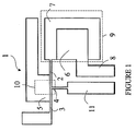
- a typical electrochemical pixel device is shown schematically in figure 1 .
- the electrochemical pixel device 1 is constructed through patterning of a suitable material (see above), and comprises an electrochemical transistor device (2-5, 10-11) and an electrochromic device (6-9).
- the electrochemical transistor device which does not form part of the present invention, comprises a source contact 2 and a drain contact 3. Between, and in direct electrical contact with, the source and drain contacts is arranged an electrochemically active element 4, the conductivity of which may be altered through application of a gate voltage to a positive gate electrode 5.
- the electrochemically active element 4 and part of the positive gate electrode 5 are covered with a layer of solidified electrolyte 10.
- the source and drain contacts 2,3 and the electrochemically active element 4 are all formed by a continuous piece of the material. This piece is separated by a narrow gap from the gate electrode 5, so that there is no direct electrical contact between the electrochemically active element 4 and the gate electrode 5.
- the electrochromic device comprises an electrochromic element 6, as well as two electrodes 7,8. Covering the electrochromic element 6 and the first electrode 7 is a layer of solidified electrolyte 9. There is no direct electrical contact between the first electrode 7 and the electrochromic element 6, but between the electrochromic element 6 and the second electrode 8.
- the first electrode 7 of the electrochromic device is in direct electrical contact with, or rather coincides with, the source contact 2 of the electrochemical transistor device.
- a colouring or decolouring current is supplied to the electrochromic element 6 through application of a voltage between drain contact 3 and electrode 8, corresponding to a drain-source-voltage V ds .
- the current actually supplied to the electrochromic element 6 is controlled by the conductivity in the electrochemically active element 4. This conductivity, in turn, is controlled by a gate voltage V g at the positive gate electrode 5.
- the gate voltage V g may, in certain embodiments, be applied between the positive gate electrode 5 and a second, negative gate electrode 11, which may or may not be in direct electrical contact with the electrochemically active element 4.
- the gate voltage is applied between the positive gate electrode 5 and either of the source contact 2 or the drain contact 3.
- the above described embodiment of the electrochromic device is thus interconnected with a transistor, which is used for driving the device.
- the transistor does however not form part of the present invention, but only serves as an example of a possible application for the invention. Of course, in many applications the transistor can be left out. This is the case, for example, when the electrochromic device is to be passively addressed. Such a passive device of course can be formed similar to the above embodiment, only by omitting the transistor.
- An embodiment of such an electrochromical device is illustrated in Figure 2 , which in effect is an identical device as the one shown in Figure 1 , but having the transistor omitted.
- the device was manufactured as follows: a starting material of OrgaconTM EL-350 foil, commercially available from Agfa and comprising the conducting and electrochromic polymer PEDOT-PSS (poly-(3,4-ethylendioxythiophene) doped with poly(styrene sulfonate)) was used. Patterning of the PEDOT-PSS substrate was done using a plotter tool equipped with a scalpel. The electrolyte used was commercially available Bl ⁇ gelTM from Apoteksbolaget, Sweden. The gel was applied using silk-screen printing with a 45 ⁇ m thick, patterned vinyl foil as template. Alternatively, 10% hydroxy ethyl cellulose in water may be used as the electrolyte gel.
- PEDOT-PSS poly-(3,4-ethylendioxythiophene) doped with poly(styrene sulfonate)
- PEDOT-PSS is a material that exhibits a very light, pale blue colour and good conductivity in its native, partly oxidised state. When the PEDOT-PSS is reduced, its conductivity diminishes greatly, and the material is coloured deeply blue.
- the electrochromic device is typically driven with V ds voltages between 1.5 and 2 V, and the display area varies between 1 and 2 cm 2 .
- the electrochromic element 6 in this case is reduced and switched to a deep blue colour.
- An electrode 7 converts the electronic current to ionic current or vice versa is also present.
- the current passing through the electrochromic device was about 200-300 ⁇ A in the beginning, at a V ds of 2 V and an electrochromic element area of 1-2 cm 2 . After approximately 10 s it was fully switched and saturated. The current flowing through the electrochromic device in this saturated state was around 50 ⁇ A. The reason for this current even in the reduced, non-conducting state of PEDOT-PSS is leakage from the display cell.
- the electrochemical transistor device was driven by gate voltages between 0 and 1.5 V.
- the electrochemically active element was fully conducting, and at 1.5 V, it was in its "off' state.
- the resistance in the transistor channel was approximately around 10 k ⁇ in its conducting state, which corresponded to a current of 200 ⁇ A at 2 V.
- the resistance was greatly increased.
- Current values of around 200 nA were reached, corresponding to a resistance of 10 M ⁇ .
- the on/off-ratio for the electrochemical transistor device part of the electrochemical pixel device was thus 1000 in this case.
- extreme on/off-ratios of 10 5 in the electrochemical transistor were reached with components made in alternative ways.
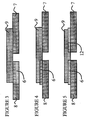
- Figure 3 illustrates a electrochemical device, in which the electrochemical element 6 and the electrodes 7 and 8 are all placed side by side, and the electrochromical element is place at a distance from electrode 7 and in direct electrical contact with electrode 8.
- Figure 4 illustrates an alternative arrangement, in which the electrochemically active element 6 is instead placed on top of the electrode 8.
- Figure 5 illustrates a similar arrangement as the one illustrated in Figure 4 , but having an additional, protective layer 12 deposited on electrode 7.
- the protective layer 12 serves to protect the electrode 7 from being overoxidised when exposed to an oxidative current.
- Figure 6 illustrates an inventive electrochemical element, comprising mixture layer 602 of PEDOT-PSS mixed with polystyrene and a protective layer 601 comprising PANI. At the interface between layers 601 and 602 there is formed an intermediate layer 603, which is the result of solvents in the PANI soloutin dissolving and mixing with the surface of the PEDOT-PSS layer.
- Such an intermediate layer is actually the reason explaining the improved adhesion of the PANI layer to the PEDOT-PSS layer.
- a intermediate layer 603 might not be formed, the layers 601 and 602 instead being in direct contact with each other.
- the protective PANI layer serves to protect the mixture layer from being overoxidised, and also provides the element with switchable redox properties.
- the test architecture thus comprises a counter electrode 702 and a pixel electrode 701.
- an electrochromic element 703 is defined, and on the counter electrode a counter electrode area 704 is defined.
- This counter electrode area 704 is actually also an electrochromic element in the following examples.
- a solidified electrolyte 705 is deposited.
- the electrolyte is based on water and contains 10% by weight of hydroxyethyl cellulose, 20% by weight of glycerol, 8% by weight of sodium citrate salt (Na-citrate). The pH value of the electrolyte is adjusted to between 4 and 5 by adding H 3 PO 4 prior to applying the electrolyte onto the device.
- Electrodes 701 and 702 were formed from an OrgaconTM EL-350 foil. In this case the PEDOT-PSS functions both as conductors and electrodes in the device.
- the counter electrode 702 was coated with PANIPOL TTM deposited by drop casting. An identical device is made up as reference from the same components but without the PANI layer.
- the pixels were switched continuously in forward bias 1.5V where the electrochromical element turns transparent and in backward bias 9.0V where the pixel element turns blue.
- the cycling was continued for 1 000 cycles and the pixel and counter electrodes were checked for overoxidation.
- the PANI covered counter electrode was nearly unaffected (less than 1 % degradation of the active area) but the counter electrode of the reference device was completely degraded after 1000 switches.
- the PANI coated device actually continued to switch for over 10 000 switches and its lifetime was limited not due to overoxidation but due to delamination of the PANI from the PEDOT-PSS layer. This delamination is believed to be the effect of, at least partially, the different swelling properties of the two materials, PEDOT-PSS and PANI, which caused mechanical strains during electrochemical switching.
- the PEDOT-PSS used in the counter electrode part of the device here was a screen printable paste, Orgacon ELTM, as supplied by Agfa.
- Orgacon ELTM screen printable paste
- PANIPOL TTM solution On top of the screen-printed counter electrode part of the device was drop casted a PANIPOL TTM solution.
- the pixel was switched continuously in forward bias 1.5V where the pixel elements turn transparent and in backward bias 9.0V were the pixel elements turn blue.
- the cycling was continued for 10 000 cycles and the pixel and counter electrode were checked for overoxidation and delamination. No significant delamination or degradation of the counter electrode could be observed.
- the device was kept switching for over 25 000 switches and still no significant degradation of the counter electrode or delamination could be observed.
- the same architecture as in the above example was used.
- the electrodes were formed from OrgaconTM EL-350.
- the pixels were switched continuously in forward bias 1.5V where the pixel element turns transparent and in backward bias 1,5V were the pixel element turns blue. The cycling was continued for 10 cycles when the pixel and counter electrodes were assumed to have reached "equilibrium conditions".
- the contrast was measured using a spectrometer. The wavelength used was 640nm.
- the contrast ratios were compared, in a forward bias of 1.5 V were the PEDOT-PSS pixel turns transparent and the PANI coated PEDOT-PSS pixel becomes blue and in a backward bias of 1.5 V were the PEDOT-PSS pixel turns blue and the PANI coated PEDOT-PSS pixel becomes transparent.
- the different contrasts using the Lab vector length in the CIE-Lab colour coordinates were for the PEDOT-PSS pixel 4 and for the PANI coated PEDOT-PSS pixel it was 20.
Claims (12)
- Elektrochemisch aktives Element, umfassend:- eine erste Schicht, die Poly-(3,4-ethylendioxythiophen) umfasst, das mit Poly(styrolsulfonat) dotiert ist (PEDOT-PSS); und- eine zweite Schicht, die Polyanilin (PANI) umfasst,dadurch gekennzeichnet, dass- die zweite Schicht sich in direktem elektrischem Kontakt mit der ersten Schicht befindet; und- die erste Schicht PEDOT-PSS, gemischt mit einem Haftvermittler, umfasst.
- Elektrochemisch aktives Element nach Anspruch 1, wobei der Haftvermittler Polystyrol umfasst.
- Elektrochemisch aktives Element nach einem der Ansprüche 1 oder 2, wobei das PANI aus einer Toluenlösung abgegossen ist.
- Elektrochemisch aktives Element nach einem der vorherigen Ansprüche, wobei der Haftvermittler ein Material umfasst, das aus der Gruppe bestehend aus Polystyrol, Latexformulierungen, Poly(methylmetaacrylat), Polyurethanen, Polyglycolestern, N-Vinyllactamen, Gelatine, einem Gelatinederivat, Polyacrylsäuren oder - estern, Polymethacrylsäure, Poly(vinylpyrrolidon), Polysacchariden, Hydroxyethylcellulose und anderen Cellulosederivaten, Polyacrylamiden, Polyurethanen, Polypropylenoxiden, Polyethylenoxiden, Poly(styrolsulphonsäure), Poly(styrolsulphonestern), Poly(vinylalkoholestern) und Poly(vinylalkohol) und Derivaten, Salzen, Mischungen und Copolymeren derselben ausgewählt ist.
- Elektrochemisch aktives Element nach einem der vorherigen Ansprüche, das ferner einen erstarrten Elektrolyten umfasst, welcher sich in direktem Kontakt mit einer der Schichten befindet.
- Elektrochemisch aktives Element nach Anspruch 5, wobei die zweite Schicht auf der ersten Schicht abgeschieden ist.
- Elektrochemisch aktives Element nach einem der vorherigen Ansprüche, das Teil einer Pixelvorrichtung bildet.
- Elektrochemisch aktives Element nach einem der Ansprüche 7, wobei die Pixelvorrichtung eine laterale Pixelvorrichtung ist.
- Elektrochemisch aktives Element nach einem der Ansprüche 7, wobei die Pixelvorrichtung eine vertikale Pixelvorrichtung ist.
- Elektrochemisch aktives Element nach einem der Ansprüche 1 bis 6, das Teil einer Transistorvorrichtung bildet.
- Elektrochemisch aktives Element nach einem der Ansprüche 1 bis 6, das Teil einer Diodenvorrichtung bildet.
- Verfahren zum Herstellen eines elektrochemisch aktiven Elementes, das die folgenden Schritte umfasst:- Anordnen einer ersten und zweiten Elektrode auf einem Substrat, wobei die Elektroden PEDOT-PSS umfassen;gekennzeichnet durch die folgenden Schritte- Drucken einer Schicht von PANI auf der ersten Elektrode; und- Auftragen einer Schicht von Elektrolyt in Kontakt mit mindestens einem Teil der PANI-Schicht und in Kontakt mit mindestens einem Teil der zweiten Elektrode; wobei- die erste und zweite Elektrode auf dem Substrat durch Drucken angeordnet sind, und- die Elektroden PEDOT-PSS, gemischt mit einem Haftvermittler, umfassen.
Applications Claiming Priority (3)
| Application Number | Priority Date | Filing Date | Title |
|---|---|---|---|
| US10/091,397 US6642069B2 (en) | 2001-03-07 | 2002-03-07 | Electrochemical pixel device |
| PCT/SE2002/000404 WO2002071139A1 (en) | 2001-03-07 | 2002-03-07 | Electrochemical pixel device |
| EP03708782A EP1487935A1 (de) | 2002-03-07 | 2003-03-07 | Elektrochemische vorrichtung |
Related Parent Applications (2)
| Application Number | Title | Priority Date | Filing Date |
|---|---|---|---|
| EP03708782A Division EP1487935A1 (de) | 2002-03-07 | 2003-03-07 | Elektrochemische vorrichtung |
| EP03708782.2 Division | 2003-03-07 |
Publications (3)
| Publication Number | Publication Date |
|---|---|
| EP2015135A2 EP2015135A2 (de) | 2009-01-14 |
| EP2015135A3 EP2015135A3 (de) | 2009-12-16 |
| EP2015135B1 true EP2015135B1 (de) | 2012-02-01 |
Family
ID=27791085
Family Applications (2)
| Application Number | Title | Priority Date | Filing Date |
|---|---|---|---|
| EP08167926A Expired - Lifetime EP2015135B1 (de) | 2002-03-07 | 2003-03-07 | Elektrochemische Vorrichtung |
| EP03708782A Withdrawn EP1487935A1 (de) | 2002-03-07 | 2003-03-07 | Elektrochemische vorrichtung |
Family Applications After (1)
| Application Number | Title | Priority Date | Filing Date |
|---|---|---|---|
| EP03708782A Withdrawn EP1487935A1 (de) | 2002-03-07 | 2003-03-07 | Elektrochemische vorrichtung |
Country Status (5)
| Country | Link |
|---|---|
| US (2) | US7158277B2 (de) |
| EP (2) | EP2015135B1 (de) |
| JP (1) | JP4532908B2 (de) |
| AU (1) | AU2003212753A1 (de) |
| WO (1) | WO2003074627A1 (de) |
Cited By (1)
| Publication number | Priority date | Publication date | Assignee | Title |
|---|---|---|---|---|
| WO2018137892A1 (en) | 2017-01-30 | 2018-08-02 | Saralon Gmbh | Method of producing pedot:pss based electrodes |
Families Citing this family (69)
| Publication number | Priority date | Publication date | Assignee | Title |
|---|---|---|---|---|
| EP2015135B1 (de) * | 2002-03-07 | 2012-02-01 | Acreo AB | Elektrochemische Vorrichtung |
| WO2005010598A2 (en) * | 2003-07-24 | 2005-02-03 | E Ink Corporation | Electro-optic displays |
| WO2005122285A2 (en) | 2004-06-04 | 2005-12-22 | The Board Of Trustees Of The University Of Illinois | Methods and devices for fabricating and assembling printable semiconductor elements |
| US7799699B2 (en) | 2004-06-04 | 2010-09-21 | The Board Of Trustees Of The University Of Illinois | Printable semiconductor structures and related methods of making and assembling |
| DE102005017682A1 (de) * | 2005-04-08 | 2006-10-12 | Varta Microbattery Gmbh | Galvanisches Element |
| JP4685507B2 (ja) * | 2005-05-19 | 2011-05-18 | 株式会社日立製作所 | エレクトロクロミックデバイス |
| US9084546B2 (en) * | 2005-08-31 | 2015-07-21 | The Regents Of The University Of Michigan | Co-electrodeposited hydrogel-conducting polymer electrodes for biomedical applications |
| US20070202648A1 (en) * | 2006-02-28 | 2007-08-30 | Samsung Electronics Co. Ltd. | Memory device and method of manufacturing the same |
| US7660029B2 (en) * | 2006-08-01 | 2010-02-09 | Universite De Moncton | Chromogenically tunable photonic crystals |
| DE102006044069A1 (de) * | 2006-09-20 | 2008-03-27 | Bayer Materialscience Ag | Elektrochrome Anordnung |
| GB0623108D0 (en) | 2006-11-20 | 2006-12-27 | Sericol Ltd | A printable composition |
| WO2008115598A1 (en) * | 2007-03-21 | 2008-09-25 | Ntera, Inc. | Lucent technologies inc. |
| EP1988514A1 (de) * | 2007-05-04 | 2008-11-05 | Acreo AB | Schaltung für ein Sicherheitsdokument |
| US9061494B2 (en) | 2007-07-19 | 2015-06-23 | The Board Of Trustees Of The University Of Illinois | High resolution electrohydrodynamic jet printing for manufacturing systems |
| GB2454203A (en) | 2007-10-30 | 2009-05-06 | Univ Muenster Wilhelms | Time controlled activation of elements |
| US9782949B2 (en) | 2008-05-30 | 2017-10-10 | Corning Incorporated | Glass laminated articles and layered articles |
| US8097926B2 (en) | 2008-10-07 | 2012-01-17 | Mc10, Inc. | Systems, methods, and devices having stretchable integrated circuitry for sensing and delivering therapy |
| US8372726B2 (en) * | 2008-10-07 | 2013-02-12 | Mc10, Inc. | Methods and applications of non-planar imaging arrays |
| US8389862B2 (en) | 2008-10-07 | 2013-03-05 | Mc10, Inc. | Extremely stretchable electronics |
| US9289132B2 (en) * | 2008-10-07 | 2016-03-22 | Mc10, Inc. | Catheter balloon having stretchable integrated circuitry and sensor array |
| US8886334B2 (en) * | 2008-10-07 | 2014-11-11 | Mc10, Inc. | Systems, methods, and devices using stretchable or flexible electronics for medical applications |
| FR2937154B1 (fr) | 2008-10-09 | 2010-11-19 | Essilor Int | Systeme electroactif transparent |
| WO2010099147A1 (en) * | 2009-02-24 | 2010-09-02 | Ntera Inc. | Advanced electrode structures and electrochromic devices |
| GB0904263D0 (en) | 2009-03-12 | 2009-04-22 | Sericol Ltd | Electrolyte composition |
| EP2430652B1 (de) | 2009-05-12 | 2019-11-20 | The Board of Trustees of the University of Illionis | Bedruckte anordnungen aus ultradünnen und mikrofeinen anorganischen leds für verformbare und semitransparente anzeigen |
| PT104635A (pt) | 2009-06-16 | 2010-12-16 | Univ Nova De Lisboa | Dispositivo electrocrómico e método para a sua produção |
| US9723122B2 (en) | 2009-10-01 | 2017-08-01 | Mc10, Inc. | Protective cases with integrated electronics |
| US20110218756A1 (en) * | 2009-10-01 | 2011-09-08 | Mc10, Inc. | Methods and apparatus for conformal sensing of force and/or acceleration at a person's head |
| WO2011042430A1 (en) | 2009-10-05 | 2011-04-14 | Acreo Ab | Electrochemical device |
| JP5593389B2 (ja) * | 2009-10-05 | 2014-09-24 | アクレオ スウェディッシュ イーセーティー アーベー | アクティブ・マトリックス・エレクトロクロミック・ディスプレイ・デバイス、及び、その製造方法 |
| EP2334151A1 (de) * | 2009-12-10 | 2011-06-15 | Bayer MaterialScience AG | Verfahren zur Herstellung eines Elektrolumineszenz-Elements mittels Sprühapplikation auf beliebig geformten Gegenständen |
| US10441185B2 (en) | 2009-12-16 | 2019-10-15 | The Board Of Trustees Of The University Of Illinois | Flexible and stretchable electronic systems for epidermal electronics |
| US9936574B2 (en) | 2009-12-16 | 2018-04-03 | The Board Of Trustees Of The University Of Illinois | Waterproof stretchable optoelectronics |
| JP6046491B2 (ja) | 2009-12-16 | 2016-12-21 | ザ ボード オブ トラスティーズ オブ ザ ユニヴァーシティー オブ イリノイ | コンフォーマル電子機器を使用した生体内での電気生理学 |
| US9057994B2 (en) * | 2010-01-08 | 2015-06-16 | The Board Of Trustees Of The University Of Illinois | High resolution printing of charge |
| CN102892356B (zh) | 2010-03-17 | 2016-01-13 | 伊利诺伊大学评议会 | 基于生物可吸收基质的可植入生物医学装置 |
| US9709867B2 (en) | 2010-10-05 | 2017-07-18 | Rise Acreo Ab | Display device |
| EP2439584A1 (de) * | 2010-10-05 | 2012-04-11 | Acreo AB | Verfahren zur Herstellung einer elektrochemischen Vorrichtung |
| US8562095B2 (en) | 2010-11-01 | 2013-10-22 | The Board Of Trustees Of The University Of Illinois | High resolution sensing and control of electrohydrodynamic jet printing |
| EP2695020B1 (de) | 2011-04-05 | 2016-05-18 | Acreo Swedish ICT AB | Verfahren zur herstellung einer elektrochemisch aktiven vorrichtung beruhend auf der selbstausrichtung von elektrolyten auf elektroden |
| WO2012158709A1 (en) | 2011-05-16 | 2012-11-22 | The Board Of Trustees Of The University Of Illinois | Thermally managed led arrays assembled by printing |
| KR102000302B1 (ko) | 2011-05-27 | 2019-07-15 | 엠씨10, 인크 | 전자, 광학, 및/또는 기계 장치 및 시스템, 그리고 이를 제조하기 위한 방법 |
| EP2713863B1 (de) | 2011-06-03 | 2020-01-15 | The Board of Trustees of the University of Illionis | Anpassbare aktiv multiplexierte elektrodenanordnung mit hochdichter oberfläche zur elektrophysiologischen messung am gehirn |
| JP6222848B2 (ja) * | 2011-11-07 | 2017-11-01 | リセ アクレオ アーベー | 縦型エレクトロクロミック・ディスプレイ |
| KR101979354B1 (ko) | 2011-12-01 | 2019-08-29 | 더 보오드 오브 트러스티스 오브 더 유니버시티 오브 일리노이즈 | 프로그램 변형을 실행하도록 설계된 과도 장치 |
| EP2794281A4 (de) * | 2011-12-20 | 2015-07-22 | Univ Connecticut | Hochauflösende strukturierung auf leitfähigem gewebe durch tintenstrahldruck und anwendung echte tragbare anzeigevorrichtungen |
| EP2607950B1 (de) | 2011-12-22 | 2014-05-21 | Acreo Swedish ICT AB | Standbildanzeigevorrichtung und Verfahren zu ihrer Herstellung |
| PT106070A (pt) | 2011-12-23 | 2013-06-24 | Yd Ynvisible S A | Solução de electrólito, método de impressão da mesma e electrólito sólido resultante |
| EP2629245A3 (de) * | 2012-02-16 | 2013-08-28 | Acreo Swedish ICT AB | Datenmatrixcodeanordnung mit Display und Herstellungsverfahren dafürr |
| CN105283122B (zh) | 2012-03-30 | 2020-02-18 | 伊利诺伊大学评议会 | 可共形于表面的可安装于附肢的电子器件 |
| WO2013161633A1 (ja) | 2012-04-23 | 2013-10-31 | 株式会社村田製作所 | 導電性組成物、複合材料およびそれらの製造方法 |
| US9171794B2 (en) | 2012-10-09 | 2015-10-27 | Mc10, Inc. | Embedding thin chips in polymer |
| EP2730973A1 (de) * | 2012-11-09 | 2014-05-14 | Acreo Swedish ICT AB | Standbilderzeugungsvorrichtung und Verfahren zu ihrer Herstellung |
| FR3003044B1 (fr) * | 2013-03-07 | 2016-07-29 | Centre Nat Rech Scient | Dispositif electrochrome a quatre ou trois couches |
| US9235044B2 (en) | 2014-01-29 | 2016-01-12 | The Gillette Company | Light activated power indicator |
| BR112017025609A2 (pt) | 2015-06-01 | 2018-08-07 | The Board Of Trustees Of The University Of Illinois | sistemas eletrônicos miniaturizados com potência sem fio e capacidades de comunicação de campo próximo |
| KR20180034342A (ko) | 2015-06-01 | 2018-04-04 | 더 보드 오브 트러스티즈 오브 더 유니버시티 오브 일리노이 | 대안적인 자외선 감지방법 |
| US10925543B2 (en) | 2015-11-11 | 2021-02-23 | The Board Of Trustees Of The University Of Illinois | Bioresorbable silicon electronics for transient implants |
| US11086184B1 (en) * | 2016-04-20 | 2021-08-10 | Kinestral Technologies, Inc | Electrochromic devices having optimized visual characteristics |
| FR3067477A1 (fr) * | 2017-06-07 | 2018-12-14 | Ecole Nationale Superieure des Arts et Industries Textiles | Structure electro chromique comportant une couche support deformable |
| EP3674791B1 (de) * | 2017-08-23 | 2022-07-20 | National Institute for Materials Science | Elektrochromes element und anzeigesystem damit |
| US10801990B2 (en) * | 2018-04-17 | 2020-10-13 | Hach Company | Alkalinity measurement of an aqueous sample |
| EP3785280A4 (de) | 2018-04-24 | 2022-03-23 | University of Connecticut | Flexibles textilantennensystem mit leitfähigen polymeren und verfahren zur herstellung davon |
| CN109521621A (zh) * | 2018-12-28 | 2019-03-26 | 五邑大学 | 一种肩并肩结构的电致变色器件及其应用 |
| CN110262152A (zh) * | 2019-06-17 | 2019-09-20 | 浙江工业大学 | 一种高颜色对比度的电致变色器件及其组装方法 |
| FR3113958B1 (fr) * | 2020-09-08 | 2023-03-31 | Univ Bordeaux | Dispositif électrochrome |
| WO2022104099A1 (en) * | 2020-11-12 | 2022-05-19 | Jumbe Nelson L | Transducers, their methods of manufacture and uses |
| JPWO2022181760A1 (de) * | 2021-02-26 | 2022-09-01 | ||
| CN113406834A (zh) * | 2021-06-01 | 2021-09-17 | Oppo广东移动通信有限公司 | 电子设备、壳体组件以及变色膜片 |
Family Cites Families (28)
| Publication number | Priority date | Publication date | Assignee | Title |
|---|---|---|---|---|
| DE3721793A1 (de) * | 1986-07-01 | 1988-04-07 | Mitsubishi Electric Corp | Elektrisches element mit verwendung von oxidations-reduktions-substanzen |
| US4993810A (en) * | 1989-04-14 | 1991-02-19 | Ford Motor Company | Electrochromic devices comprising metal salts in an ion conductive material |
| US5049868A (en) * | 1989-09-19 | 1991-09-17 | Rockwell International Corporation | Electrochromic display dot drive matrix |
| IT1237269B (it) * | 1989-11-15 | 1993-05-27 | Rete neurale con capacita' di apprendimento per il trattamento di informazioni, e procedimento per il trattamento di informazioni con l'impiego di tale rete. | |
| GB9000238D0 (en) * | 1990-01-05 | 1990-03-07 | Rca Licensing Corp | Minimum power standby circuit arrangement |
| EP0440957B1 (de) * | 1990-02-08 | 1996-03-27 | Bayer Ag | Neue Polythiophen-Dispersionen, ihre Herstellung und ihre Verwendung |
| US5189549A (en) * | 1990-02-26 | 1993-02-23 | Molecular Displays, Inc. | Electrochromic, electroluminescent and electrochemiluminescent displays |
| FR2664430B1 (fr) * | 1990-07-04 | 1992-09-18 | Centre Nat Rech Scient | Transistor a effet de champ en couche mince de structure mis, dont l'isolant et le semiconducteur sont realises en materiaux organiques. |
| US5138481A (en) * | 1991-07-23 | 1992-08-11 | Ford Motor Company | Electrochromic device with color gradient and method of making the device |
| US5413739A (en) * | 1992-12-22 | 1995-05-09 | Coleman; James P. | Electrochromic materials and displays |
| US5754329A (en) | 1992-12-22 | 1998-05-19 | Monsanto Company | Electrochromic display laminates |
| WO1994016356A1 (en) * | 1993-01-05 | 1994-07-21 | Martin Marietta Corporation | Improved electrode for display devices |
| FR2746934B1 (fr) * | 1996-03-27 | 1998-05-07 | Saint Gobain Vitrage | Dispositif electrochimique |
| US6369934B1 (en) * | 1996-05-30 | 2002-04-09 | Midwest Research Institute | Self bleaching photoelectrochemical-electrochromic device |
| DE19622600C2 (de) * | 1996-06-05 | 2001-08-02 | Fraunhofer Ges Forschung | Elektrochrome Einheit |
| GB2324883A (en) * | 1997-04-28 | 1998-11-04 | Wisconsin Label Corp | Self-powered electrochemical display cell with focused field |
| US5877888A (en) * | 1997-06-10 | 1999-03-02 | Monsanto Company | Single and double sided electrochromic displays |
| EP0968537B1 (de) | 1997-08-22 | 2012-05-02 | Creator Technology B.V. | Feld-effekt-transistor, der im wesentlichen aus organischen materialien besteht |
| DE19810932A1 (de) * | 1998-03-13 | 1999-09-16 | Bayer Ag | Elektrochrome Anordnung auf Basis von Poly-(3,4-ethylendioxy-thiophen)-Derivaten |
| US6118572A (en) * | 1998-07-01 | 2000-09-12 | The Regents Of The University Of California | Photochromic, electrochromic, photoelectrochromic and photovoltaic devices |
| US6506438B2 (en) * | 1998-12-15 | 2003-01-14 | E Ink Corporation | Method for printing of transistor arrays on plastic substrates |
| US6387727B1 (en) | 1999-03-29 | 2002-05-14 | Agere Systems Guardian Corp. | Device comprising n-channel semiconductor material |
| US6444400B1 (en) * | 1999-08-23 | 2002-09-03 | Agfa-Gevaert | Method of making an electroconductive pattern on a support |
| GB9924515D0 (en) * | 1999-10-15 | 1999-12-15 | Cambridge Display Tech Ltd | Light-emitting devices |
| DE60214833T2 (de) * | 2001-03-07 | 2007-09-06 | Acreo Ab | Elektrochromische einrichtung |
| JP4256163B2 (ja) * | 2001-03-07 | 2009-04-22 | アクレオ アーベー | 電気化学ピクセル装置 |
| KR100424090B1 (ko) * | 2001-06-25 | 2004-03-22 | 삼성에스디아이 주식회사 | 유기 전계 발광 소자용 정공 수송층, 그 정공 수송층을사용한유기 전계 발광 소자 및 그 소자의 제조 방법 |
| EP2015135B1 (de) * | 2002-03-07 | 2012-02-01 | Acreo AB | Elektrochemische Vorrichtung |
-
2003
- 2003-03-07 EP EP08167926A patent/EP2015135B1/de not_active Expired - Lifetime
- 2003-03-07 JP JP2003573083A patent/JP4532908B2/ja not_active Expired - Fee Related
- 2003-03-07 US US10/505,573 patent/US7158277B2/en not_active Expired - Lifetime
- 2003-03-07 EP EP03708782A patent/EP1487935A1/de not_active Withdrawn
- 2003-03-07 WO PCT/SE2003/000393 patent/WO2003074627A1/en active Application Filing
- 2003-03-07 AU AU2003212753A patent/AU2003212753A1/en not_active Abandoned
-
2006
- 2006-12-05 US US11/633,548 patent/US7301687B2/en not_active Expired - Fee Related
Cited By (1)
| Publication number | Priority date | Publication date | Assignee | Title |
|---|---|---|---|---|
| WO2018137892A1 (en) | 2017-01-30 | 2018-08-02 | Saralon Gmbh | Method of producing pedot:pss based electrodes |
Also Published As
| Publication number | Publication date |
|---|---|
| US7301687B2 (en) | 2007-11-27 |
| US20050068603A1 (en) | 2005-03-31 |
| EP1487935A1 (de) | 2004-12-22 |
| US20070076287A1 (en) | 2007-04-05 |
| WO2003074627A1 (en) | 2003-09-12 |
| US7158277B2 (en) | 2007-01-02 |
| EP2015135A3 (de) | 2009-12-16 |
| AU2003212753A1 (en) | 2003-09-16 |
| EP2015135A2 (de) | 2009-01-14 |
| JP4532908B2 (ja) | 2010-08-25 |
| JP2005519316A (ja) | 2005-06-30 |
Similar Documents
| Publication | Publication Date | Title |
|---|---|---|
| EP2015135B1 (de) | Elektrochemische Vorrichtung | |
| EP1373976B1 (de) | Elektrochemische pixel-einrichtung | |
| EP1373975B1 (de) | Elektrochromische einrichtung | |
| US8233211B2 (en) | Electrochromic display device and its manufacturing method | |
| Heuer et al. | Electrochromic window based on conducting poly (3, 4‐ethylenedioxythiophene)–poly (styrene sulfonate) | |
| US7333257B2 (en) | Device for contacting patterned electrodes on porous substrates | |
| Mecerreyes et al. | A simplified all-polymer flexible electrochromic device | |
| US7746533B2 (en) | Electrochromic devices utilizing very low band gap conjugated counter electrodes: preparation and use | |
| US20020158295A1 (en) | Electrochemical device | |
| KR101761850B1 (ko) | 전기화학 장치 | |
| US20120081775A1 (en) | Display device | |
| JP2006030820A (ja) | 表示装置および表示方法 | |
| JPWO2009031422A1 (ja) | エレクトロクロミック表示素子の製造方法 | |
| CN1304897C (zh) | 电化学器件 | |
| EP2439584A1 (de) | Verfahren zur Herstellung einer elektrochemischen Vorrichtung | |
| SE521552C2 (sv) | Elektrokromatisk anordning och förfarande för tillverkning av anordningen |
Legal Events
| Date | Code | Title | Description |
|---|---|---|---|
| PUAI | Public reference made under article 153(3) epc to a published international application that has entered the european phase |
Free format text: ORIGINAL CODE: 0009012 |
|
| AC | Divisional application: reference to earlier application |
Ref document number: 1487935 Country of ref document: EP Kind code of ref document: P |
|
| AK | Designated contracting states |
Kind code of ref document: A2 Designated state(s): AT BE BG CH CY CZ DE DK EE ES FI FR GB GR HU IE IT LI LU MC NL PT RO SE SI SK TR |
|
| RIN1 | Information on inventor provided before grant (corrected) |
Inventor name: KUGLER, THOMAS Inventor name: BERGGREN, MAGNUS Inventor name: MALMSTROEM, ANNA Inventor name: KAELL, JESSICA Inventor name: REMONEN, TOMMI |
|
| PUAL | Search report despatched |
Free format text: ORIGINAL CODE: 0009013 |
|
| AK | Designated contracting states |
Kind code of ref document: A3 Designated state(s): AT BE BG CH CY CZ DE DK EE ES FI FR GB GR HU IE IT LI LU MC NL PT RO SE SI SK TR |
|
| 17P | Request for examination filed |
Effective date: 20100611 |
|
| AKX | Designation fees paid |
Designated state(s): AT BE BG CH CY LI |
|
| REG | Reference to a national code |
Ref country code: DE Ref legal event code: 8566 |
|
| 17Q | First examination report despatched |
Effective date: 20100920 |
|
| RBV | Designated contracting states (corrected) |
Designated state(s): AT BE BG CH CY CZ LI |
|
| RBV | Designated contracting states (corrected) |
Designated state(s): AT BE BG CH CY CZ DE DK EE ES FI FR GB GR HU IE IT LI LU MC NL PT RO SE SI SK TR |
|
| GRAP | Despatch of communication of intention to grant a patent |
Free format text: ORIGINAL CODE: EPIDOSNIGR1 |
|
| GRAS | Grant fee paid |
Free format text: ORIGINAL CODE: EPIDOSNIGR3 |
|
| GRAA | (expected) grant |
Free format text: ORIGINAL CODE: 0009210 |
|
| AC | Divisional application: reference to earlier application |
Ref document number: 1487935 Country of ref document: EP Kind code of ref document: P |
|
| AK | Designated contracting states |
Kind code of ref document: B1 Designated state(s): AT BE BG CH CY CZ DE DK EE ES FI FR GB GR HU IE IT LI LU MC NL PT RO SE SI SK TR |
|
| REG | Reference to a national code |
Ref country code: GB Ref legal event code: FG4D |
|
| REG | Reference to a national code |
Ref country code: AT Ref legal event code: REF Ref document number: 544092 Country of ref document: AT Kind code of ref document: T Effective date: 20120215 Ref country code: CH Ref legal event code: EP |
|
| REG | Reference to a national code |
Ref country code: DE Ref legal event code: R096 Ref document number: 60339931 Country of ref document: DE Effective date: 20120322 |
|
| REG | Reference to a national code |
Ref country code: SE Ref legal event code: TRGR |
|
| REG | Reference to a national code |
Ref country code: NL Ref legal event code: VDEP Effective date: 20120201 |
|
| PG25 | Lapsed in a contracting state [announced via postgrant information from national office to epo] |
Ref country code: NL Free format text: LAPSE BECAUSE OF FAILURE TO SUBMIT A TRANSLATION OF THE DESCRIPTION OR TO PAY THE FEE WITHIN THE PRESCRIBED TIME-LIMIT Effective date: 20120201 |
|
| PG25 | Lapsed in a contracting state [announced via postgrant information from national office to epo] |
Ref country code: PT Free format text: LAPSE BECAUSE OF FAILURE TO SUBMIT A TRANSLATION OF THE DESCRIPTION OR TO PAY THE FEE WITHIN THE PRESCRIBED TIME-LIMIT Effective date: 20120601 Ref country code: GR Free format text: LAPSE BECAUSE OF FAILURE TO SUBMIT A TRANSLATION OF THE DESCRIPTION OR TO PAY THE FEE WITHIN THE PRESCRIBED TIME-LIMIT Effective date: 20120502 Ref country code: BE Free format text: LAPSE BECAUSE OF FAILURE TO SUBMIT A TRANSLATION OF THE DESCRIPTION OR TO PAY THE FEE WITHIN THE PRESCRIBED TIME-LIMIT Effective date: 20120201 Ref country code: FI Free format text: LAPSE BECAUSE OF FAILURE TO SUBMIT A TRANSLATION OF THE DESCRIPTION OR TO PAY THE FEE WITHIN THE PRESCRIBED TIME-LIMIT Effective date: 20120201 |
|
| REG | Reference to a national code |
Ref country code: AT Ref legal event code: MK05 Ref document number: 544092 Country of ref document: AT Kind code of ref document: T Effective date: 20120201 |
|
| PG25 | Lapsed in a contracting state [announced via postgrant information from national office to epo] |
Ref country code: CY Free format text: LAPSE BECAUSE OF FAILURE TO SUBMIT A TRANSLATION OF THE DESCRIPTION OR TO PAY THE FEE WITHIN THE PRESCRIBED TIME-LIMIT Effective date: 20120201 |
|
| PG25 | Lapsed in a contracting state [announced via postgrant information from national office to epo] |
Ref country code: RO Free format text: LAPSE BECAUSE OF FAILURE TO SUBMIT A TRANSLATION OF THE DESCRIPTION OR TO PAY THE FEE WITHIN THE PRESCRIBED TIME-LIMIT Effective date: 20120201 Ref country code: EE Free format text: LAPSE BECAUSE OF FAILURE TO SUBMIT A TRANSLATION OF THE DESCRIPTION OR TO PAY THE FEE WITHIN THE PRESCRIBED TIME-LIMIT Effective date: 20120201 Ref country code: SI Free format text: LAPSE BECAUSE OF FAILURE TO SUBMIT A TRANSLATION OF THE DESCRIPTION OR TO PAY THE FEE WITHIN THE PRESCRIBED TIME-LIMIT Effective date: 20120201 Ref country code: DK Free format text: LAPSE BECAUSE OF FAILURE TO SUBMIT A TRANSLATION OF THE DESCRIPTION OR TO PAY THE FEE WITHIN THE PRESCRIBED TIME-LIMIT Effective date: 20120201 Ref country code: MC Free format text: LAPSE BECAUSE OF NON-PAYMENT OF DUE FEES Effective date: 20120331 Ref country code: CZ Free format text: LAPSE BECAUSE OF FAILURE TO SUBMIT A TRANSLATION OF THE DESCRIPTION OR TO PAY THE FEE WITHIN THE PRESCRIBED TIME-LIMIT Effective date: 20120201 |
|
| REG | Reference to a national code |
Ref country code: CH Ref legal event code: PL |
|
| PG25 | Lapsed in a contracting state [announced via postgrant information from national office to epo] |
Ref country code: SK Free format text: LAPSE BECAUSE OF FAILURE TO SUBMIT A TRANSLATION OF THE DESCRIPTION OR TO PAY THE FEE WITHIN THE PRESCRIBED TIME-LIMIT Effective date: 20120201 Ref country code: IT Free format text: LAPSE BECAUSE OF FAILURE TO SUBMIT A TRANSLATION OF THE DESCRIPTION OR TO PAY THE FEE WITHIN THE PRESCRIBED TIME-LIMIT Effective date: 20120201 |
|
| PLBE | No opposition filed within time limit |
Free format text: ORIGINAL CODE: 0009261 |
|
| STAA | Information on the status of an ep patent application or granted ep patent |
Free format text: STATUS: NO OPPOSITION FILED WITHIN TIME LIMIT |
|
| REG | Reference to a national code |
Ref country code: IE Ref legal event code: MM4A |
|
| 26N | No opposition filed |
Effective date: 20121105 |
|
| PG25 | Lapsed in a contracting state [announced via postgrant information from national office to epo] |
Ref country code: AT Free format text: LAPSE BECAUSE OF FAILURE TO SUBMIT A TRANSLATION OF THE DESCRIPTION OR TO PAY THE FEE WITHIN THE PRESCRIBED TIME-LIMIT Effective date: 20120201 Ref country code: CH Free format text: LAPSE BECAUSE OF NON-PAYMENT OF DUE FEES Effective date: 20120331 Ref country code: IE Free format text: LAPSE BECAUSE OF NON-PAYMENT OF DUE FEES Effective date: 20120307 Ref country code: LI Free format text: LAPSE BECAUSE OF NON-PAYMENT OF DUE FEES Effective date: 20120331 |
|
| REG | Reference to a national code |
Ref country code: DE Ref legal event code: R097 Ref document number: 60339931 Country of ref document: DE Effective date: 20121105 |
|
| PG25 | Lapsed in a contracting state [announced via postgrant information from national office to epo] |
Ref country code: ES Free format text: LAPSE BECAUSE OF FAILURE TO SUBMIT A TRANSLATION OF THE DESCRIPTION OR TO PAY THE FEE WITHIN THE PRESCRIBED TIME-LIMIT Effective date: 20120512 |
|
| PG25 | Lapsed in a contracting state [announced via postgrant information from national office to epo] |
Ref country code: BG Free format text: LAPSE BECAUSE OF FAILURE TO SUBMIT A TRANSLATION OF THE DESCRIPTION OR TO PAY THE FEE WITHIN THE PRESCRIBED TIME-LIMIT Effective date: 20120501 |
|
| PG25 | Lapsed in a contracting state [announced via postgrant information from national office to epo] |
Ref country code: TR Free format text: LAPSE BECAUSE OF FAILURE TO SUBMIT A TRANSLATION OF THE DESCRIPTION OR TO PAY THE FEE WITHIN THE PRESCRIBED TIME-LIMIT Effective date: 20120201 |
|
| PG25 | Lapsed in a contracting state [announced via postgrant information from national office to epo] |
Ref country code: LU Free format text: LAPSE BECAUSE OF NON-PAYMENT OF DUE FEES Effective date: 20120307 |
|
| PG25 | Lapsed in a contracting state [announced via postgrant information from national office to epo] |
Ref country code: HU Free format text: LAPSE BECAUSE OF FAILURE TO SUBMIT A TRANSLATION OF THE DESCRIPTION OR TO PAY THE FEE WITHIN THE PRESCRIBED TIME-LIMIT Effective date: 20030307 |
|
| PGFP | Annual fee paid to national office [announced via postgrant information from national office to epo] |
Ref country code: SE Payment date: 20150318 Year of fee payment: 13 |
|
| REG | Reference to a national code |
Ref country code: FR Ref legal event code: PLFP Year of fee payment: 14 |
|
| REG | Reference to a national code |
Ref country code: SE Ref legal event code: EUG |
|
| PG25 | Lapsed in a contracting state [announced via postgrant information from national office to epo] |
Ref country code: SE Free format text: LAPSE BECAUSE OF NON-PAYMENT OF DUE FEES Effective date: 20160308 |
|
| REG | Reference to a national code |
Ref country code: FR Ref legal event code: PLFP Year of fee payment: 15 |
|
| REG | Reference to a national code |
Ref country code: FR Ref legal event code: PLFP Year of fee payment: 16 |
|
| PGFP | Annual fee paid to national office [announced via postgrant information from national office to epo] |
Ref country code: GB Payment date: 20220216 Year of fee payment: 20 Ref country code: DE Payment date: 20220217 Year of fee payment: 20 |
|
| PGFP | Annual fee paid to national office [announced via postgrant information from national office to epo] |
Ref country code: FR Payment date: 20220216 Year of fee payment: 20 |
|
| REG | Reference to a national code |
Ref country code: DE Ref legal event code: R071 Ref document number: 60339931 Country of ref document: DE |
|
| REG | Reference to a national code |
Ref country code: GB Ref legal event code: PE20 Expiry date: 20230306 |
|
| PG25 | Lapsed in a contracting state [announced via postgrant information from national office to epo] |
Ref country code: GB Free format text: LAPSE BECAUSE OF EXPIRATION OF PROTECTION Effective date: 20230306 |