EP2010500B1 - Anordnung zur kontaktierung von leistungshalbleitern an einer kühlfläche - Google Patents
Anordnung zur kontaktierung von leistungshalbleitern an einer kühlfläche Download PDFInfo
- Publication number
- EP2010500B1 EP2010500B1 EP07727781A EP07727781A EP2010500B1 EP 2010500 B1 EP2010500 B1 EP 2010500B1 EP 07727781 A EP07727781 A EP 07727781A EP 07727781 A EP07727781 A EP 07727781A EP 2010500 B1 EP2010500 B1 EP 2010500B1
- Authority
- EP
- European Patent Office
- Prior art keywords
- spring element
- cooling surface
- housing
- arrangement according
- spring
- Prior art date
- Legal status (The legal status is an assumption and is not a legal conclusion. Google has not performed a legal analysis and makes no representation as to the accuracy of the status listed.)
- Active
Links
Images
Classifications
-
- H—ELECTRICITY
- H10—SEMICONDUCTOR DEVICES; ELECTRIC SOLID-STATE DEVICES NOT OTHERWISE PROVIDED FOR
- H10W—GENERIC PACKAGES, INTERCONNECTIONS, CONNECTORS OR OTHER CONSTRUCTIONAL DETAILS OF DEVICES COVERED BY CLASS H10
- H10W40/00—Arrangements for thermal protection or thermal control
- H10W40/60—Securing means for detachable heating or cooling arrangements, e.g. clamps
- H10W40/641—Snap-on arrangements, e.g. clips
-
- A—HUMAN NECESSITIES
- A61—MEDICAL OR VETERINARY SCIENCE; HYGIENE
- A61P—SPECIFIC THERAPEUTIC ACTIVITY OF CHEMICAL COMPOUNDS OR MEDICINAL PREPARATIONS
- A61P35/00—Antineoplastic agents
-
- H—ELECTRICITY
- H05—ELECTRIC TECHNIQUES NOT OTHERWISE PROVIDED FOR
- H05K—PRINTED CIRCUITS; CASINGS OR CONSTRUCTIONAL DETAILS OF ELECTRIC APPARATUS; MANUFACTURE OF ASSEMBLAGES OF ELECTRICAL COMPONENTS
- H05K7/00—Constructional details common to different types of electric apparatus
- H05K7/20—Modifications to facilitate cooling, ventilating, or heating
- H05K7/2089—Modifications to facilitate cooling, ventilating, or heating for power electronics, e.g. for inverters for controlling motor
- H05K7/209—Heat transfer by conduction from internal heat source to heat radiating structure
Definitions
- the present invention relates to an arrangement for contacting at least one electronic component mounted in a housing with connecting wires, in particular a power semiconductor, on a cooling surface and a spring element fastened in the housing with at least one spring arm which presses the component against the cooling surface in a contact position of the spring element ,
- the prior art further includes holding devices, which essentially comprise a U- or L-shaped spring clip which is (clipped ”) over ade Economicswandung and simultaneously over the component and in this way the pressing force between the contact surfaces of the heat sink and ensures the component.
- the present invention is based on the object to provide an arrangement of the type described above, which exerts no shear forces in the direction or opposite direction of the connecting wires for the electrical components with simple installation.
- the above-mentioned object is achieved in that the housing wall in the adjoining the side wall acting as a cooling surface side walls perpendicular to the bottom to running embedded pairs of grooves, each consisting of an insertion groove and a locking groove, wherein the Einhegenuten are deart .
- the locking grooves allow a convenient automatic engagement of the spring element in a predefined position. A complex alignment of the spring element is eliminated.
- the spring element is displaceable from the first mounting position by a force perpendicular to the cooling surface in the pressing position, so that in this second assembly step no thrust force acts in the longitudinal direction of the connecting wires, instead, the spring element from the first mounting position by acting purely perpendicular to the cooling surface forces fixed in the pressure position.
- the spring element consists of mutually parallel spring arms, which are perpendicularly attached to a support member which connects the two lateral projections of the spring element with each other
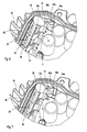
- the Fig. 1 and 2 show an inventive spring element 2 as provided for installation in an electronics housing 4 of an electric motor.
- the spring element 2 consists of a support member 8, at the upper edge present z. B. six spring arms 10 are formed and the side has two angled lugs 12 a, 12 b.
- the lugs 12a, 12b are formed at their upper and lower edges with folded at right angles inwardly tabs 13 to prevent buckling of the lugs 12a, 12b.
- the support member has approximately right angle folded narrow portions 14a, 14b, the bottom portion 14a facing the side where the spring arms 10 are and the top portion 14b faces in the opposite direction.
- the upper section 14b continues at equidistant intervals ( Fig.
- the spring arms 10 At its lower end, the spring arms 10 have a convex outwardly curved contact portion 16 which in Anyakposition of the spring element 2 against the Components 24 presses.
- a convex outwardly curved contact portion 16 Below the center of the support member 8, opposite the contact portions 16, parallel to the top and bottom edges of the support member 8 is a curved towards the front, semicircular stiffening bead 18, which prevents bending of the spring element 2.
- the Fig. 3 to 7 show a possible use variant of the spring element 2 according to the invention in an electronics housing 4 of an electric motor 6.
- the electronics housing 4 On a rotor housing 7 of the electric motor 6, the electronics housing 4 is placed, which receives a printed circuit board 20 with electronic components 22 and other electrical connecting elements ( Fig. 3 ).
- the electronics housing 4 consists essentially of a peripheral wall, which is formed by a flat side wall 26, which acts as a cooling surface, adjoining side walls 32, 33 and one of the planar side wall 26 opposite wall 34.
- brackets 36 are formed with holes 37 for attachment of the housing.
- the electronics housing 4 can be closed with a housing cover, not shown, which engages in a circumferential groove 38 on the end face of the side walls 26, 32, 33 and 34.
- the housing cover is attached to holding projections 40, the holes 41, attached.
- On the bottom of the electronics housing 4 sits a electronic components 22, 24 supporting circuit board 20.
- Power semiconductors 24 are soldered to the circuit board 20 that they can be arranged in the interior of the electronics housing 4 on a flat side wall 26 of the electronics housing 4. Between the power semiconductor 24 and the planar side wall 26, a heat conductive electrical insulating layer 28 is inserted to allow and improve heat transfer to the side wall 26 provided with cooling fins 30.
- the upper pair of tabs 13 has an additional task: If the * spring element 2 is inserted into the electronics housing 4, but not yet locked, a housing cover can not be mounted, as then molded on the housing cover pin on the upper tabs 13th rest and would prevent closure of the lid. If the proper locking of the spring element 2 is performed, the pin of the lid can engage in the vacant space and the lid can be put on. This has a check whether a proper assembly of the spring element 2 has been performed.
- the insertion position is in Fig. 4 shown. A detailed view of the position of the spring element in this insertion position shows Fig. 6 , It can be seen that the projection 12a is fixed by placing its end portion in the insertion groove 44a. In the insertion process, the spring arms 10 are not yet in contact with the power semiconductors 24, thus exerting no shear forces on the component 24 and its solder joint. It an air gap 45 remains between the spring arms 10 and the power semiconductors 24.
- the latching groove pair 46a, 46b adjoins directly to the insertion grooves 44a, 44b and is recessed in the same way but at a smaller distance from the flat side wall 26.
- the transition region 48a, 48b between the insertion groove 44a (44b) and the latching groove 46a (46b) is formed in such a way that its resistance can be overcome by a force F acting on the spring element 2 perpendicular to the cooling surface ( Fig. 4 ).
- the elastic lateral projections 12a, 12b are briefly compressed during the advancing movement in the direction of the power semiconductor 24 by the transition regions 48a, 48b before they rest in the latching grooves 46a, 46b in the pressure position ( Fig. 5 ).
- FIG. 7 A detailed view of the position of the spring element 2 on the side wall 32 in the pressure position shows Fig. 7 , The end portion of the projection 12a fixed with its vertically extending edge, which is now embedded in the locking groove 46a, the spring element 2.
- this pressure position now press the spring arms 10 on the power semiconductor 24, which thereby against the heat-conducting insulating layer 28 and thus against as Cooling surface 27 formed side wall 26 are pressed. This ensures safe heat dissipation without the use of other fasteners, such as screws or clamps.
- the component 24 and the solder joint are not loaded by shear forces.
Landscapes
- Engineering & Computer Science (AREA)
- Microelectronics & Electronic Packaging (AREA)
- Physics & Mathematics (AREA)
- Thermal Sciences (AREA)
- Health & Medical Sciences (AREA)
- Chemical & Material Sciences (AREA)
- Chemical Kinetics & Catalysis (AREA)
- General Chemical & Material Sciences (AREA)
- Medicinal Chemistry (AREA)
- Nuclear Medicine, Radiotherapy & Molecular Imaging (AREA)
- Organic Chemistry (AREA)
- Pharmacology & Pharmacy (AREA)
- Life Sciences & Earth Sciences (AREA)
- Animal Behavior & Ethology (AREA)
- General Health & Medical Sciences (AREA)
- Public Health (AREA)
- Veterinary Medicine (AREA)
- Cooling Or The Like Of Electrical Apparatus (AREA)
- Cooling Or The Like Of Semiconductors Or Solid State Devices (AREA)
Description
- Die vorliegende Erfindung betrifft eine Anordnung zur Kontaktierung von mindestens einem in einem Gehäuse mit Anschlussdrähten montiertem elektronischen Bauelement, insbesondere einem Leistungshalbleiter, an einer Kühlfläche und einem im Gehäuse befestigbaren Federelement mit mindestens einem Federarm, der in einer Andruckposition des Federelements das Bauelement gegen die Kühlfläche drückt.
- Um die Kühlung von Leistungshalbleitern zu gewährleisten, werden diese in wärmeleitenden Kontakt zu einem Kühlkörper gesetzt. Dies wird in kostengünstigen Ausführungen meist mit Federn realisiert, die das Halbleiterbauelement an den Kühlkörper pressen.
- Eine solche Anordnung ist in der deutschen Gebrauchsmusterschrift
G 92 13 671.0 beschrieben. Durch die Vormontage eines Haltefederelements in einem Gehäuseteil werden bei anschließendem Zusammensetzen der Gehäuseteile die zu kühlenden Bauelemente durch Federzungen der Haltefeder gegen eine Innenwand des Kühlkörpers gedrückt. - In ähnlicher Weise zeigen die
US-Patentschrift 5,274,193 , die deutsche Offenlegungsschrift36 12 862 A1 , die deutsche Patentschrift195 43 260 C2 und die deutsche GebrauchsmusterschriftDE 200 14 739 U1 Federelement, die zwischen Leistungshalbleitern und Gehäuse verklemmt werden. Unterschiedlich ist jeweils die Abstützung bzw. die Befestigung der Federelemente an dem Gehäuse. So kann beispielsweise das Federelement selbst durch Ausnehmungen und Stege des Gehäuses gehalten werden oder mittels zusätzlicher Befestigungselemente wie Schrauben oder Klemmschienen gehalten werden. - Dem Stand der Technik gehören weiterhin Haltevorrichtungen an, die im Wesentlichen einen U- oder L-förmigen Federbügel aufweisen, der über eine Kühlkörperwandung und gleichzeitig über das Bauelement gesteckt ("geclipt") wird und auf diese Weise die Andruckkraft zwischen den Anlageflächen des Kühlkörpers und des Bauelements sicherstellt.
- Bei allen Vorrichtungen ohne zusätzliche Befestigungselemente, aus dem deutschen Gebrauchsmuster G 92 13 671.0 bekannt, tritt das Problem auf, dass das Bauteil und die Lötstelle durch Schubspannungen belastet werden. Dies kann zu einer Schädigung des Bauteils oder der Lötverbindung führen. Die Schubspannungen entstehen durch Kräfte, die beim Zusammenbau der Vorrichtung in einer Ebene parallel zur Kohlanlagefläche der Bauelemente bzw. des Kühlkörpers auf das Bauelement einwirken.
- In dem im
US-Patent 5,274,193 offenbarten Gegenstand wirkt zwar keine Schubkraft auf die Bauelemente, die Fixierung der Haltefeder und das Erzeugen der Haltekraft des Federelements muss aber durch eine zusätzliche Klemmschiene bewerkstelligt werden. - Aus der
US 5,909,358 ist eine gattungsgemäße Anordnung bekannt. Bei dieser bekannten Anordnung muss das Federelement beim Übergang in die Andruckposition eine Art Schwenkbewegung durchführen und zudem erfolgt die Montage des Federelements senkrecht zur Kühlfläche, so dass ein relativ großer Platzbedarf vor der Kühlfläche für das Einführen des Federelements erforderlich ist - Eine entsprechende Montage erfolgt auch bei dem Federelement, wie es aus der
DE 103 17182 A1 bekannt ist. - Auch das aus der
FR 2780456 - Der vorliegenden Erfindung liegt die Aufgabe zu Grunde, eine Anordnung der eingangs beschriebenen Art zu schaffen, die bei einfacher Montage keine Schubkräfte in Richtung oder Gegenrichtung der Anschlussdrähte für die elektrischen Bauelemente ausübt.
- Eine Anordnung gemäß dem Oberbegriff des Patentanspruchs 1 ist aus
US 5,909,358 bekannt. - Erfindungsgemäß wird die oben erwähnte Aufgabe dadurch erreicht, dass die Gehäusewandung in den an die als Kühlfläche wirkende seitlichen Wand angrenzenden Seitenwänden senkrecht nach unten auf den Boden zu verlaufende eingelassene Nutenpaare aufweist, die jeweils aus einer Einfügenut und einer Rastnut bestehen, wobei die Einfügenuten deart sind, dass das Federelement in axialer Richtung der Einfügenuten gegenüber dem Leistungshalbleiter berührungsfrei parallel zur Kühlfläche in einer Einfügeposition mittels seitlich an einem Trägerelement des Federelements abgewinkelter elastischer Ansätze einschiebbar ist, und die Rastnuten mit den Einfügenuten über derart angeformte Übergangsbereiche verbunden sind, dass das in der Einfügeposition befindliche Federelement mittels der Ansätze durch eine senkrecht zur Kühlfläche wirkenden Kraft in die Rastnuten in die Andruckposition rastend verschiebbar ist und die Rastnuten derart ausgebildet sind, dass das Federelement in der Andruckposition halten.
- Die Rastnuten ermöglichen ein zweckmäßiges automatisches Einrasten des Federelements in vordefinierter Position. Eine aufwändige Ausrichtung des Federelements entfällt.
- Das Federelement ist von der ersten Montageposition durch eine Kraftwirkung senkrecht zur Kühlfläche in die Andruckposition verschiebbar, so dass bei diesem zweiten Montageschritt keine Schubkraft in Längsrichtung der Anschlussdrähte wirkt, statt dessen wird das Federelement aus der ersten Montageposition heraus durch rein senkrecht auf die Kühlfläche wirkende Kräfte in der Andruckposition fixiert.
- In weiterer vorteilhafter Ausgestaltung besteht das Federelement aus parallel zueinander verlaufenden Federarmen, die senkrecht an einem Trägerelement befestigt sind, das die beiden seitlichen Ansätze des Federelements miteinander verbindet Diese Ausführung erlaubt es auf Grund der Steifigkeit hohe Anpresskräfte aufzubringen, wobei vorteilhafterweise nur ein Federelement für alle gleichförmig angeordneten Halbleiterbauelemente erforderlich ist.
- Weitere zweckmäßige Ausgestaltungsmerkmale werden an Hand eines bevorzugten, in den Zeichnungen veranschaulichten Ausführungsbeispiels genau erläutert. Dabei zeigen:
- Fig. 1
- eine Vorderansicht eines erfindungsgemäßen Federelements,
- Fig. 2
- eine rückwärtige Ansicht des erfindungsgemäßen Federelements,
- Fig. 3
- das Federelement vor dem Einsatz in ein Elektronikgehäuse,
- Fig. 4
- das Federelement in einer ersten Montageposition,
- Fig. 5
- das Federelement in eingerasteter Andruckposition,
- Fig. 6
- Detailansicht des Federelements in der ersten Montageposition,
- Fig. 7
- Detailansicht des Federelements in eingerasteter Andruckposition.
- Die
Fig. 1 und 2 zeigen ein erfindungsgemäßes Federelement 2 wie es zum Einbau in ein Elektronikgehäuse 4 eines Elektromotors vorgesehen ist. Das Federelement 2 besteht aus einem Trägerelement 8, an dessen oberer Kante vorliegend z. B. sechs Federarme 10 angeformt sind und das seitlich zwei abgewinkelte Ansätze 12a, 12b aufweist. Die Ansätze 12a, 12b sind an ihrer oberen und unteren Kante mit rechtwinklig nach innen umgefalzten Laschen 13 ausgebildet, um ein Einknicken der Ansätze 12a, 12b zu verhindern. An der Ober- und Unterkante besitzt das Trägerelement ebenfalls etwa rechtwinklig umgefalzte schmale Abschnitte 14a, 14b, wobei der untere Abschnitt 14a zu der Seite weist, an der sich die Federarme 10 befinden und der obere Abschnitt 14b in die entgegengesetzte Richtung weist. Der obere Abschnitt 14b setzt sich in äquidistanten Abständen fort (Fig. 2 ) und bildet über die Oberkante des Trägerelements 8 nach unten in Richtung auf den Abschnitt 14 a gebogen die parallel zueinander verlaufenden Federarme 10. An ihrem unteren Ende besitzen die Federarme 10 einen nach außen konvex gekrümmten Kontaktbereich 16, der in Andruckposition des Federelements 2 gegen die Bauelemente 24 drückt. Unterhalb der Mitte des Trägerelements 8, gegenüberliegend der Kontaktbereiche 16, verläuft parallel zur Ober- und Unterkante des Trägerelements 8 eine zur Vorderseite hin gewölbte, halbkreisförmige Versteifungssicke 18, die ein Durchbiegen des Federelements 2 verhindert. - Die
Fig. 3 bis 7 zeigen eine mögliche Verwendungsvariante des erfindungsgemäßen Federelementes 2 in einem Elektronikgehäuse 4 eines Elektromotors 6. Auf ein Rotorgehäuse 7 des Elektromotors 6 ist das Elektronikgehäuse 4 aufgesetzt, das eine Leiterplatte 20 mit elektronischen Bauelementen 22 sowie weitere elektrische Verbindungselemente aufnimmt (Fig. 3 ). Das Elektronikgehäuse 4 besteht im Wesentlichen aus einer Umfangswandung, die von einer ebenen seitlichen Wand 26, die als Kühlfläche wirkt, daran angrenzenden Seitenwänden 32, 33 und einer der ebenen seitlichen Wand 26 gegenüberliegenden Wand 34 gebildet wird. An den Seitenwänden 32, 33 sowie an der gegenüberliegenden Wand 34 sind Halterungen 36 mit Bohrungen 37 zur Befestigung des Gehäuses angeformt. Das Elektronikgehäuse 4 kann mit einem nicht dargestellten Gehäusedeckel verschlossen werden, der in eine umlaufende Nut 38 an der Stirnseite der Seitenwände 26, 32, 33 und 34 eingreift. Der Gehäusedeckel ist an Haltevorsprüngen 40, die Bohrungen 41 aufweisen, befestigt. Auf dem Boden des Elektronikgehäuses 4 sitzt eine die elektronischen Bauelemente 22, 24 tragende Leiterplatte 20. Dabei sind Leistungshalbleiter 24 so auf der Leiterplatte 20 eingelötet, dass sie im Innern des Elektronikgehäuses 4 an einer ebenen seitlichen Wand 26 des Elektronikgehäuses 4 angeordnet werden können. Zwischen dem Leistungshalbleiter 24 und der ebenen Seitenwand 26 ist eine wärmeleitende elektrische Isolierschicht 28 eingefügt, um einen Wärmetransport zu der mit Kühlrippen 30 versehenen Seitenwand 26 zu ermöglichen und zu verbessern. - In die an die ebene Seitenwand 26 angrenzenden Seitenwände 32 und 33 sind senkrecht nach unten verlaufende Nutpaare eingelassen, die die Funktion als Einfügenuten 44a, 44b und als Rastnuten 46a, 46b erfüllen. Die zwei Einfügenuten 44a, 44b befinden sich beiseitig der ebenen Seitenwand 26 in jeweils gleichem Abstand von dieser einander gegenüber in den Seitenwänden 32, 33. In diese Einfügenuten 44a, 44b wird das Federelement 2 axial entsprechend der Pfeilrichtung R in
Fig. 3 eingeschoben und nimmt eine erste Montageposition (Einfügeposition) ein. Die an der Oberseite angebrachten Laschen 13 können dabei als Angriffsflächen für die per Hand aufgebrachten Einschubkräfte dienen. Neben dieser Funktion als Montagehilfe besitzt das obere Laschenpaar 13 noch eine zusätzliche Aufgabe: Wenn das *Federelement 2 in das Elektronikgehäuse 4 eingesetzt, aber noch nicht verrastet ist, lässt sich ein Gehäusedeckel nicht montieren, da am Gehäusedeckel angespritzte Zapfen dann auf den oberen Laschen 13 aufliegen und ein Schließen des Deckels verhindern würden. Ist die ordnungsgemäße Verrastung des Federelementes 2 durchgeführt, kann der Zapfen des Deckels in den frei gewordenen Raum eingreifen und der Deckel lässt sich aufsetzen. Man hat hierdurch eine Kontrolle, ob eine ordnungsgemäße Montage des Federelementes 2 durchgeführt wurde. Die Einfügeposition ist inFig. 4 dargestellt. Eine Detailansicht der Lage des Federelements in dieser Einfügeposition zeigtFig. 6 . Man erkennt, dass der Ansatz 12a durch Anlage seines Endbereichs in der Einfügenut 44a fixiert ist. Bei dem Einschubvorgang kommen die Federarme 10 noch nicht mit den Leistungshalbleitern 24 in Berührung, üben somit keinerlei Schubkräfte auf das Bauteil 24 und dessen Lötstelle aus. Es verbleibt ein Luftspalt 45 zwischen den Federarmen 10 und den Leistungshalbleitern 24. - Das Rastnutpaar 46a, 46b schließt sich unmittelbar an die Einfügenuten 44a, 44b an und ist in gleicher Weise, aber mit geringerem Abstand zur ebenen Seitenwand 26 eingelassen. Der Übergangsbereich 48a, 48b zwischen Einfügenut 44a (44b) und Rastnut 46a (46b) ist derart ausgeformt, dass dessen Widerstand durch eine Krafteinwirkung F auf das Federelement 2 senkrecht zur Kühlfläche überwunden werden kann (
Fig. 4 ). Dabei werden die elastischen seitlichen Ansätze 12a, 12b kurzzeitig bei der Vorschubbewegung in Richtung des Leistungshalbleiters 24 durch die Übergangsbereiche 48a, 48b zusammengedrückt, bevor sie in den Rastnuten 46a, 46b in der Andruckposition anliegen (Fig. 5 ). - Eine Detailansicht der Lage des Federelements 2 an der Seitenwand 32 in Andruckposition zeigt
Fig. 7 . Der Endbereich des Ansatzes 12a fixiert mit seiner senkrecht verlaufenden Kante, die jetzt in die Rastnut 46a eingebettet ist, das Federelement 2. In dieser Andruckposition drücken nun die Federarme 10 auf die Leistungshalbleiter 24, die dadurch gegen die wärmeleitende Isolierschicht 28 und damit gegen die als Kühlfläche 27 ausgebildete Seitenwand 26 gepresst werden. Dadurch wird ohne Verwendung weiterer Verbindungselemente, wie Schrauben oder Klemmen, eine sichere Wärmeableitung gewährleistet. Das Bauteil 24 und die Lötstelle werden nicht durch Schubkräfte belastet. - Die Erfindung ist nicht auf die dargestellten und beschriebenen Ausführungsbeispiele beschränkt, sondern umfaßt auch alle im Sinne der Erfindung gleichwirkenden Ausführungen.
Claims (8)
- Anordnung zur Kontakberung von mindestens einem elektronischen Bauelement (24), insbesondere einem Leistungshalbleiter (24), an einer Kühlfläche (26), bestehend aus einem Gehäuse (4), an dessen Kühlfläche (26) das elektronische Bauelement (24) mit Anschlussdrähten montiert ist und aus einem im Gehäuse (4) befestigbaren Federelement (2) mit mindestens einem Federarm (10), der in einer Andruckposition des Federelements (2) das Bauelement (24) gegen die Kühlfläche (26) drückt, und das Federelement (2) ohne Berührung des Bauelements (24) in das Gehäuse (4) einführbar ist und das Gehäuse (4) derart mit Haltemitteln (46a, 46b) für das Federelement (2) versehen ist, dass bei der Montage des Federelements (2) keine Schubkräfte in Längsrichtung der Anschlussdrähte auftreten,
dadurch gekennzeichnet, dass die Gehäusewandung in den an die als Kühlfläche wirkenden seitlichen Wand (26) angrenzenden Seitenwänden (32, 33) senkrecht nach unten auf den Boden zu verlaufende, eingelassene Nutenpaare aufweist, die jeweils aus einer Einfügenut (44a, 44b) und einer Rastnut (46a, 46b) bestehen, wobei die Einfügenuten (44a, 44b) derart sind, dass das Federelement (2) in axialer Richtung (R) der Einfügenuten gegenüber dem Leistungshalbleiter (24) berührungsfrei parallel zur Kühlfläche (26) in einer Einfügeposition mittels seitlich an einem Trägerelement des Federelements (2) abgewinkelter elastischer Ansätze (12a, 12b) einschiebbar ist, und die Rastnuten (46a, 46b) mit den Einfügenuten (44a, 44b) über derart angeformte Übergangsbereiche (48a, 48b) verbunden sind, dass das in der Einfügeposition befindliche Federelement (2) mittels der Ansätze (12a, 12b) durch eine senkrecht zur Kühlfläche (26) wirkenden Kraft (F) in die Rastnuten (46a, 46b) in die Andruckposition rastend verschiebbar ist, und die Rastnuten (46a, 46b) derart ausgebildet sind, dass sie das Federelement (2) in der Andruckposition halten. - Anordnung nach Anspruch 1,
dadurch gekennzeichnet, dass mehrereFederarme(10)parallel zueinander verlaufend an der im Montagezustand der Leiterplatte abgewandten Kante des Trägerelements (8) befestigt sind. - Anordnung nach einem der Ansprüche 1 bis 2,
dadurch gekennzeichnet, dass das Trägerelement (8) eine zwischen beiden seitlichen Ansätzen (12a, 12b) verlaufende Versteifungssicke (18) aufweist. - Anordnung nach einem der Ansprüche 1 bis 3.
dadurch gekennzeichnet, dass das Trägerelement (8) an seinen Längsseiten rechtwinklig umgefalzte Abschnitte (14a, 14b) aufweist. - Anordnung nach einem der Ansprüche 1 bis 4,
dadurch gekennzeichnet, dass die seitlichen Ansätze (12a, 12b) des Federelements (2) rechtwinklig angeformte Laschen (13) aufweisen. - Anordnung nach einem der Ansprüche 1 bis 5,
dadurch gekennzeichnet, dass mehrere in einer Reihe mit gleicher Ausrichtung angeordnete Bauelemente (24) mit einem Federelement (2) angedrückt werden. - Anordnung nach einem der Ansprüche 1 bis 6,
dadurch gekennzeichnet, dass die als Kühlfläche (26) ausgebildete seitliche Wand (26) eine in das Gehäuseinnere weisende planparallele Anlagefläche aufweist und an ihrer Außenseite mit Kühlrippen (30) versehen ist. - Anordnung nach einem der Ansprüche 1 bis 6,
dadurch gekennzeichnet, dass eine wärmeleitende Isolierschicht (28) zwischen der Kühlfläche (26) und dem Bauelement (24) angebracht ist.
Applications Claiming Priority (2)
| Application Number | Priority Date | Filing Date | Title |
|---|---|---|---|
| DE102006018716A DE102006018716A1 (de) | 2006-04-20 | 2006-04-20 | Anordnung zur Kontaktierung von Leistungshalbleitern an einer Kühlfläche |
| PCT/EP2007/053310 WO2007122084A1 (de) | 2006-04-20 | 2007-04-04 | Anordnung zur kontaktierung von leistungshalbleitern an einer kühlfläche |
Publications (2)
| Publication Number | Publication Date |
|---|---|
| EP2010500A1 EP2010500A1 (de) | 2009-01-07 |
| EP2010500B1 true EP2010500B1 (de) | 2011-06-08 |
Family
ID=38141192
Family Applications (1)
| Application Number | Title | Priority Date | Filing Date |
|---|---|---|---|
| EP07727781A Active EP2010500B1 (de) | 2006-04-20 | 2007-04-04 | Anordnung zur kontaktierung von leistungshalbleitern an einer kühlfläche |
Country Status (6)
| Country | Link |
|---|---|
| US (1) | US7845994B2 (de) |
| EP (1) | EP2010500B1 (de) |
| CN (1) | CN101421246B (de) |
| AT (1) | ATE512461T1 (de) |
| DE (1) | DE102006018716A1 (de) |
| WO (1) | WO2007122084A1 (de) |
Cited By (15)
| Publication number | Priority date | Publication date | Assignee | Title |
|---|---|---|---|---|
| US8839815B2 (en) | 2011-12-15 | 2014-09-23 | Honeywell International Inc. | Gas valve with electronic cycle counter |
| US8899264B2 (en) | 2011-12-15 | 2014-12-02 | Honeywell International Inc. | Gas valve with electronic proof of closure system |
| US8905063B2 (en) | 2011-12-15 | 2014-12-09 | Honeywell International Inc. | Gas valve with fuel rate monitor |
| US8947242B2 (en) | 2011-12-15 | 2015-02-03 | Honeywell International Inc. | Gas valve with valve leakage test |
| US9074770B2 (en) | 2011-12-15 | 2015-07-07 | Honeywell International Inc. | Gas valve with electronic valve proving system |
| US9234661B2 (en) | 2012-09-15 | 2016-01-12 | Honeywell International Inc. | Burner control system |
| US9557059B2 (en) | 2011-12-15 | 2017-01-31 | Honeywell International Inc | Gas valve with communication link |
| US9995486B2 (en) | 2011-12-15 | 2018-06-12 | Honeywell International Inc. | Gas valve with high/low gas pressure detection |
| US10024439B2 (en) | 2013-12-16 | 2018-07-17 | Honeywell International Inc. | Valve over-travel mechanism |
| US10203049B2 (en) | 2014-09-17 | 2019-02-12 | Honeywell International Inc. | Gas valve with electronic health monitoring |
| US10215291B2 (en) | 2013-10-29 | 2019-02-26 | Honeywell International Inc. | Regulating device |
| US10564062B2 (en) | 2016-10-19 | 2020-02-18 | Honeywell International Inc. | Human-machine interface for gas valve |
| US10697815B2 (en) | 2018-06-09 | 2020-06-30 | Honeywell International Inc. | System and methods for mitigating condensation in a sensor module |
| US10851993B2 (en) | 2011-12-15 | 2020-12-01 | Honeywell International Inc. | Gas valve with overpressure diagnostics |
| US11073281B2 (en) | 2017-12-29 | 2021-07-27 | Honeywell International Inc. | Closed-loop programming and control of a combustion appliance |
Families Citing this family (14)
| Publication number | Priority date | Publication date | Assignee | Title |
|---|---|---|---|---|
| PT2227078E (pt) | 2009-03-04 | 2011-11-30 | Ebm Papst Mulfingen Gmbh & Co | Componente de aperto destinado a premir componentes de potência numa superfície de refrigeração |
| JP5609596B2 (ja) * | 2010-12-01 | 2014-10-22 | アイシン・エィ・ダブリュ株式会社 | 熱源素子と熱伝導性部材との固定構造、及び熱源素子と熱伝導性部材との固定方法 |
| US8668528B2 (en) | 2011-10-28 | 2014-03-11 | Apple Inc. | Split jack assemblies and methods for making the same |
| US9835265B2 (en) | 2011-12-15 | 2017-12-05 | Honeywell International Inc. | Valve with actuator diagnostics |
| JP5892691B2 (ja) * | 2011-12-15 | 2016-03-23 | 太陽誘電株式会社 | 電子装置 |
| US9846440B2 (en) | 2011-12-15 | 2017-12-19 | Honeywell International Inc. | Valve controller configured to estimate fuel comsumption |
| JP5408285B2 (ja) * | 2012-04-27 | 2014-02-05 | ダイキン工業株式会社 | 冷却器、電装品ユニット及び冷凍装置 |
| US10422531B2 (en) | 2012-09-15 | 2019-09-24 | Honeywell International Inc. | System and approach for controlling a combustion chamber |
| US9841122B2 (en) | 2014-09-09 | 2017-12-12 | Honeywell International Inc. | Gas valve with electronic valve proving system |
| US10503181B2 (en) | 2016-01-13 | 2019-12-10 | Honeywell International Inc. | Pressure regulator |
| CN109428497B (zh) * | 2017-08-23 | 2020-09-18 | 台达电子企业管理(上海)有限公司 | 电源模块的组装结构及其组装方法 |
| EP3634096A1 (de) * | 2018-10-02 | 2020-04-08 | Mahle International GmbH | Wechselrichter |
| EP3634095B1 (de) * | 2018-10-02 | 2022-03-16 | Mahle International GmbH | Wechselrichter |
| CN109801886A (zh) * | 2019-01-08 | 2019-05-24 | 常州索维尔电子科技有限公司 | 一种压紧弹片以及散热结构 |
Family Cites Families (14)
| Publication number | Priority date | Publication date | Assignee | Title |
|---|---|---|---|---|
| US4707726A (en) | 1985-04-29 | 1987-11-17 | United Technologies Automotive, Inc. | Heat sink mounting arrangement for a semiconductor |
| DE9213671U1 (de) | 1991-11-11 | 1992-12-03 | Tridonic-Bauelemente GmbH, Dornbirn | Gehäuse für eine elektronische Schaltungsanordnung |
| US5274193A (en) | 1992-04-24 | 1993-12-28 | Chrysler Corporation | Heat sink spring and wedge assembly |
| US5466970A (en) * | 1992-08-24 | 1995-11-14 | Thermalloy, Inc. | Hooked spring clip |
| DE19543260C2 (de) | 1995-11-20 | 2001-09-20 | Robert Seuffer Gmbh & Co | Elektrische Bauelementeanordnung mit mehreren in einem Gehäuse angeordneten elektrischen Bauelementen |
| US5731955A (en) * | 1996-02-05 | 1998-03-24 | Ford Motor Company | Spring clip for electronics assembly |
| US5909358A (en) * | 1997-11-26 | 1999-06-01 | Todd Engineering Sales, Inc. | Snap-lock heat sink clip |
| FR2780456A1 (fr) | 1998-06-30 | 1999-12-31 | Valeo Electronique | Dispositif de blocage mecanique d'un element electrique ou electronique sur un support |
| JP4060510B2 (ja) | 2000-03-02 | 2008-03-12 | カルソニックカンセイ株式会社 | パワー素子の放熱部材への取付構造 |
| DE20014739U1 (de) | 2000-08-28 | 2000-12-14 | Fischer-Elektronik GmbH & Co. KG, 58511 Lüdenscheid | Vorrichtung zur Halterung von elektronischen Bauteilen |
| DE10237871B4 (de) * | 2002-08-19 | 2011-05-12 | Infineon Technologies Ag | Baugruppensystem |
| DE10317182B4 (de) * | 2003-04-15 | 2005-08-18 | Lear Corporation Gmbh & Co. Kg | Befestigungseinrichtung für mindestens ein elektronisches Bauelement an einem Kühlkörper |
| US7056144B2 (en) * | 2004-02-19 | 2006-06-06 | Hewlett-Packard Development Company, L.P. | Offset compensation system |
| US7190589B2 (en) * | 2004-10-19 | 2007-03-13 | Cinch Connectors, Inc. | Electronic control enclosure |
-
2006
- 2006-04-20 DE DE102006018716A patent/DE102006018716A1/de not_active Withdrawn
-
2007
- 2007-04-04 WO PCT/EP2007/053310 patent/WO2007122084A1/de not_active Ceased
- 2007-04-04 AT AT07727781T patent/ATE512461T1/de active
- 2007-04-04 EP EP07727781A patent/EP2010500B1/de active Active
- 2007-04-04 CN CN2007800137515A patent/CN101421246B/zh active Active
- 2007-04-04 US US12/297,837 patent/US7845994B2/en active Active
Cited By (16)
| Publication number | Priority date | Publication date | Assignee | Title |
|---|---|---|---|---|
| US10697632B2 (en) | 2011-12-15 | 2020-06-30 | Honeywell International Inc. | Gas valve with communication link |
| US8899264B2 (en) | 2011-12-15 | 2014-12-02 | Honeywell International Inc. | Gas valve with electronic proof of closure system |
| US8905063B2 (en) | 2011-12-15 | 2014-12-09 | Honeywell International Inc. | Gas valve with fuel rate monitor |
| US8947242B2 (en) | 2011-12-15 | 2015-02-03 | Honeywell International Inc. | Gas valve with valve leakage test |
| US9074770B2 (en) | 2011-12-15 | 2015-07-07 | Honeywell International Inc. | Gas valve with electronic valve proving system |
| US9557059B2 (en) | 2011-12-15 | 2017-01-31 | Honeywell International Inc | Gas valve with communication link |
| US9995486B2 (en) | 2011-12-15 | 2018-06-12 | Honeywell International Inc. | Gas valve with high/low gas pressure detection |
| US8839815B2 (en) | 2011-12-15 | 2014-09-23 | Honeywell International Inc. | Gas valve with electronic cycle counter |
| US10851993B2 (en) | 2011-12-15 | 2020-12-01 | Honeywell International Inc. | Gas valve with overpressure diagnostics |
| US9234661B2 (en) | 2012-09-15 | 2016-01-12 | Honeywell International Inc. | Burner control system |
| US10215291B2 (en) | 2013-10-29 | 2019-02-26 | Honeywell International Inc. | Regulating device |
| US10024439B2 (en) | 2013-12-16 | 2018-07-17 | Honeywell International Inc. | Valve over-travel mechanism |
| US10203049B2 (en) | 2014-09-17 | 2019-02-12 | Honeywell International Inc. | Gas valve with electronic health monitoring |
| US10564062B2 (en) | 2016-10-19 | 2020-02-18 | Honeywell International Inc. | Human-machine interface for gas valve |
| US11073281B2 (en) | 2017-12-29 | 2021-07-27 | Honeywell International Inc. | Closed-loop programming and control of a combustion appliance |
| US10697815B2 (en) | 2018-06-09 | 2020-06-30 | Honeywell International Inc. | System and methods for mitigating condensation in a sensor module |
Also Published As
| Publication number | Publication date |
|---|---|
| CN101421246A (zh) | 2009-04-29 |
| CN101421246B (zh) | 2011-07-06 |
| US7845994B2 (en) | 2010-12-07 |
| US20090239424A1 (en) | 2009-09-24 |
| EP2010500A1 (de) | 2009-01-07 |
| WO2007122084A1 (de) | 2007-11-01 |
| DE102006018716A1 (de) | 2007-10-25 |
| ATE512461T1 (de) | 2011-06-15 |
Similar Documents
| Publication | Publication Date | Title |
|---|---|---|
| EP2010500B1 (de) | Anordnung zur kontaktierung von leistungshalbleitern an einer kühlfläche | |
| DE10392749B4 (de) | Kontrollmodulgehäuse für ein Fahrzeug | |
| DE102009046014B4 (de) | Elektrisches Verbindergehäuse und Verfahren zu dessen Zusammenbau | |
| EP0446320B1 (de) | Gehäuse für eine elektronische schaltung | |
| DE19722602C2 (de) | Wärmeableitendes Gehäuse zur Aufnahme von elektrischen oder elektronischen Bauteilen | |
| DE3627372C2 (de) | ||
| WO2003107418A1 (de) | Kühlkörper | |
| WO2018219769A1 (de) | Bauteilhaltevorrichtung | |
| WO2008077858A1 (de) | Halterung | |
| DE102018106185B4 (de) | Kontaktelement mit einem Kontaktkörper und einem daran angeordneten Federelement | |
| DE102020209923B3 (de) | Schaltungsträgeranordnung und Verfahren zum Herstellen einer solchen Schaltungsträgeranordnung | |
| DE19543260C2 (de) | Elektrische Bauelementeanordnung mit mehreren in einem Gehäuse angeordneten elektrischen Bauelementen | |
| DE10317182B4 (de) | Befestigungseinrichtung für mindestens ein elektronisches Bauelement an einem Kühlkörper | |
| EP3766130B1 (de) | Kontaktelement mit einem kontaktkörper und einem daran angeordneten federelement | |
| EP2553736A2 (de) | Verbindungselement, elektrischer verbinder und verbindungsanordnung für solarzellenmodule | |
| EP0511965A1 (de) | Halterung für zu kühlende elektronische bauelemente | |
| DE10334629B3 (de) | Schaltungsmodul und Verfahren zu dessen Herstellung | |
| DE10206271A1 (de) | Wärmeableitvorrichtung | |
| DE20014739U1 (de) | Vorrichtung zur Halterung von elektronischen Bauteilen | |
| DE102015116639B4 (de) | Schnappverbindungsanordnung mit einem Schnapphakenelement und einem Schnapphakengegenelement | |
| EP1750302B1 (de) | Elektrische Bauelementanordnung | |
| DE202013104941U1 (de) | Elektrische Steckverbinderanordnung und Schirmanbindungselement hierzu | |
| EP0123040A2 (de) | Klemmbrett für elektrische oder elektronische Geräte, z.B. Überstrom-Schutzschalter | |
| DE102019134369B4 (de) | Leadframe für Drahtbauteile mit Kulissenstruktur | |
| EP1864557B1 (de) | Verfahren zur herstellung eines elektronischen gerät und elektronisches gerät |
Legal Events
| Date | Code | Title | Description |
|---|---|---|---|
| PUAI | Public reference made under article 153(3) epc to a published international application that has entered the european phase |
Free format text: ORIGINAL CODE: 0009012 |
|
| 17P | Request for examination filed |
Effective date: 20081006 |
|
| AK | Designated contracting states |
Kind code of ref document: A1 Designated state(s): AT BE BG CH CY CZ DE DK EE ES FI FR GB GR HU IE IS IT LI LT LU LV MC MT NL PL PT RO SE SI SK TR |
|
| AX | Request for extension of the european patent |
Extension state: AL BA HR MK RS |
|
| 17Q | First examination report despatched |
Effective date: 20091120 |
|
| RTI1 | Title (correction) |
Free format text: ARRANGEMENT FOR CONTACTING POWER SEMICONDUCTORS TO A COOLING SURFACE |
|
| GRAP | Despatch of communication of intention to grant a patent |
Free format text: ORIGINAL CODE: EPIDOSNIGR1 |
|
| RIC1 | Information provided on ipc code assigned before grant |
Ipc: H05K 7/20 20060101ALI20101206BHEP Ipc: H01L 23/40 20060101AFI20101206BHEP |
|
| GRAS | Grant fee paid |
Free format text: ORIGINAL CODE: EPIDOSNIGR3 |
|
| GRAA | (expected) grant |
Free format text: ORIGINAL CODE: 0009210 |
|
| AK | Designated contracting states |
Kind code of ref document: B1 Designated state(s): AT BE BG CH CY CZ DE DK EE ES FI FR GB GR HU IE IS IT LI LT LU LV MC MT NL PL PT RO SE SI SK TR |
|
| REG | Reference to a national code |
Ref country code: GB Ref legal event code: FG4D Free format text: NOT ENGLISH |
|
| REG | Reference to a national code |
Ref country code: CH Ref legal event code: EP |
|
| REG | Reference to a national code |
Ref country code: IE Ref legal event code: FG4D Free format text: LANGUAGE OF EP DOCUMENT: GERMAN |
|
| REG | Reference to a national code |
Ref country code: DE Ref legal event code: R096 Ref document number: 502007007381 Country of ref document: DE Effective date: 20110721 |
|
| REG | Reference to a national code |
Ref country code: SE Ref legal event code: TRGR |
|
| REG | Reference to a national code |
Ref country code: NL Ref legal event code: VDEP Effective date: 20110608 |
|
| PG25 | Lapsed in a contracting state [announced via postgrant information from national office to epo] |
Ref country code: LT Free format text: LAPSE BECAUSE OF FAILURE TO SUBMIT A TRANSLATION OF THE DESCRIPTION OR TO PAY THE FEE WITHIN THE PRESCRIBED TIME-LIMIT Effective date: 20110608 |
|
| PG25 | Lapsed in a contracting state [announced via postgrant information from national office to epo] |
Ref country code: FI Free format text: LAPSE BECAUSE OF FAILURE TO SUBMIT A TRANSLATION OF THE DESCRIPTION OR TO PAY THE FEE WITHIN THE PRESCRIBED TIME-LIMIT Effective date: 20110608 Ref country code: SI Free format text: LAPSE BECAUSE OF FAILURE TO SUBMIT A TRANSLATION OF THE DESCRIPTION OR TO PAY THE FEE WITHIN THE PRESCRIBED TIME-LIMIT Effective date: 20110608 Ref country code: ES Free format text: LAPSE BECAUSE OF FAILURE TO SUBMIT A TRANSLATION OF THE DESCRIPTION OR TO PAY THE FEE WITHIN THE PRESCRIBED TIME-LIMIT Effective date: 20110919 Ref country code: LV Free format text: LAPSE BECAUSE OF FAILURE TO SUBMIT A TRANSLATION OF THE DESCRIPTION OR TO PAY THE FEE WITHIN THE PRESCRIBED TIME-LIMIT Effective date: 20110608 Ref country code: GR Free format text: LAPSE BECAUSE OF FAILURE TO SUBMIT A TRANSLATION OF THE DESCRIPTION OR TO PAY THE FEE WITHIN THE PRESCRIBED TIME-LIMIT Effective date: 20110909 Ref country code: CY Free format text: LAPSE BECAUSE OF FAILURE TO SUBMIT A TRANSLATION OF THE DESCRIPTION OR TO PAY THE FEE WITHIN THE PRESCRIBED TIME-LIMIT Effective date: 20110608 |
|
| PG25 | Lapsed in a contracting state [announced via postgrant information from national office to epo] |
Ref country code: NL Free format text: LAPSE BECAUSE OF FAILURE TO SUBMIT A TRANSLATION OF THE DESCRIPTION OR TO PAY THE FEE WITHIN THE PRESCRIBED TIME-LIMIT Effective date: 20110608 |
|
| REG | Reference to a national code |
Ref country code: IE Ref legal event code: FD4D |
|
| PG25 | Lapsed in a contracting state [announced via postgrant information from national office to epo] |
Ref country code: IE Free format text: LAPSE BECAUSE OF FAILURE TO SUBMIT A TRANSLATION OF THE DESCRIPTION OR TO PAY THE FEE WITHIN THE PRESCRIBED TIME-LIMIT Effective date: 20110608 Ref country code: PT Free format text: LAPSE BECAUSE OF FAILURE TO SUBMIT A TRANSLATION OF THE DESCRIPTION OR TO PAY THE FEE WITHIN THE PRESCRIBED TIME-LIMIT Effective date: 20111010 Ref country code: IS Free format text: LAPSE BECAUSE OF FAILURE TO SUBMIT A TRANSLATION OF THE DESCRIPTION OR TO PAY THE FEE WITHIN THE PRESCRIBED TIME-LIMIT Effective date: 20111008 Ref country code: EE Free format text: LAPSE BECAUSE OF FAILURE TO SUBMIT A TRANSLATION OF THE DESCRIPTION OR TO PAY THE FEE WITHIN THE PRESCRIBED TIME-LIMIT Effective date: 20110608 Ref country code: CZ Free format text: LAPSE BECAUSE OF FAILURE TO SUBMIT A TRANSLATION OF THE DESCRIPTION OR TO PAY THE FEE WITHIN THE PRESCRIBED TIME-LIMIT Effective date: 20110608 |
|
| PG25 | Lapsed in a contracting state [announced via postgrant information from national office to epo] |
Ref country code: PL Free format text: LAPSE BECAUSE OF FAILURE TO SUBMIT A TRANSLATION OF THE DESCRIPTION OR TO PAY THE FEE WITHIN THE PRESCRIBED TIME-LIMIT Effective date: 20110608 Ref country code: RO Free format text: LAPSE BECAUSE OF FAILURE TO SUBMIT A TRANSLATION OF THE DESCRIPTION OR TO PAY THE FEE WITHIN THE PRESCRIBED TIME-LIMIT Effective date: 20110608 Ref country code: SK Free format text: LAPSE BECAUSE OF FAILURE TO SUBMIT A TRANSLATION OF THE DESCRIPTION OR TO PAY THE FEE WITHIN THE PRESCRIBED TIME-LIMIT Effective date: 20110608 |
|
| PLBE | No opposition filed within time limit |
Free format text: ORIGINAL CODE: 0009261 |
|
| STAA | Information on the status of an ep patent application or granted ep patent |
Free format text: STATUS: NO OPPOSITION FILED WITHIN TIME LIMIT |
|
| 26N | No opposition filed |
Effective date: 20120309 |
|
| PG25 | Lapsed in a contracting state [announced via postgrant information from national office to epo] |
Ref country code: DK Free format text: LAPSE BECAUSE OF FAILURE TO SUBMIT A TRANSLATION OF THE DESCRIPTION OR TO PAY THE FEE WITHIN THE PRESCRIBED TIME-LIMIT Effective date: 20110608 |
|
| REG | Reference to a national code |
Ref country code: DE Ref legal event code: R097 Ref document number: 502007007381 Country of ref document: DE Effective date: 20120309 |
|
| BERE | Be: lapsed |
Owner name: EBM-PAPST MULFINGEN G.M.B.H. & CO. KG Effective date: 20120430 |
|
| PG25 | Lapsed in a contracting state [announced via postgrant information from national office to epo] |
Ref country code: MC Free format text: LAPSE BECAUSE OF NON-PAYMENT OF DUE FEES Effective date: 20120430 |
|
| REG | Reference to a national code |
Ref country code: CH Ref legal event code: PL |
|
| GBPC | Gb: european patent ceased through non-payment of renewal fee |
Effective date: 20120404 |
|
| PG25 | Lapsed in a contracting state [announced via postgrant information from national office to epo] |
Ref country code: LI Free format text: LAPSE BECAUSE OF NON-PAYMENT OF DUE FEES Effective date: 20120430 Ref country code: CH Free format text: LAPSE BECAUSE OF NON-PAYMENT OF DUE FEES Effective date: 20120430 Ref country code: BE Free format text: LAPSE BECAUSE OF NON-PAYMENT OF DUE FEES Effective date: 20120430 Ref country code: GB Free format text: LAPSE BECAUSE OF NON-PAYMENT OF DUE FEES Effective date: 20120404 |
|
| REG | Reference to a national code |
Ref country code: AT Ref legal event code: MM01 Ref document number: 512461 Country of ref document: AT Kind code of ref document: T Effective date: 20120404 |
|
| PG25 | Lapsed in a contracting state [announced via postgrant information from national office to epo] |
Ref country code: BG Free format text: LAPSE BECAUSE OF FAILURE TO SUBMIT A TRANSLATION OF THE DESCRIPTION OR TO PAY THE FEE WITHIN THE PRESCRIBED TIME-LIMIT Effective date: 20110908 |
|
| PG25 | Lapsed in a contracting state [announced via postgrant information from national office to epo] |
Ref country code: AT Free format text: LAPSE BECAUSE OF NON-PAYMENT OF DUE FEES Effective date: 20120404 Ref country code: MT Free format text: LAPSE BECAUSE OF FAILURE TO SUBMIT A TRANSLATION OF THE DESCRIPTION OR TO PAY THE FEE WITHIN THE PRESCRIBED TIME-LIMIT Effective date: 20110608 |
|
| PG25 | Lapsed in a contracting state [announced via postgrant information from national office to epo] |
Ref country code: TR Free format text: LAPSE BECAUSE OF FAILURE TO SUBMIT A TRANSLATION OF THE DESCRIPTION OR TO PAY THE FEE WITHIN THE PRESCRIBED TIME-LIMIT Effective date: 20110608 |
|
| PG25 | Lapsed in a contracting state [announced via postgrant information from national office to epo] |
Ref country code: LU Free format text: LAPSE BECAUSE OF NON-PAYMENT OF DUE FEES Effective date: 20120404 |
|
| PG25 | Lapsed in a contracting state [announced via postgrant information from national office to epo] |
Ref country code: HU Free format text: LAPSE BECAUSE OF FAILURE TO SUBMIT A TRANSLATION OF THE DESCRIPTION OR TO PAY THE FEE WITHIN THE PRESCRIBED TIME-LIMIT Effective date: 20070404 |
|
| REG | Reference to a national code |
Ref country code: FR Ref legal event code: PLFP Year of fee payment: 10 |
|
| REG | Reference to a national code |
Ref country code: FR Ref legal event code: PLFP Year of fee payment: 11 |
|
| REG | Reference to a national code |
Ref country code: FR Ref legal event code: PLFP Year of fee payment: 12 |
|
| REG | Reference to a national code |
Ref country code: DE Ref legal event code: R082 Ref document number: 502007007381 Country of ref document: DE Representative=s name: PATENTANWAELTE STAEGER & SPERLING PARTNERSCHAF, DE |
|
| PGFP | Annual fee paid to national office [announced via postgrant information from national office to epo] |
Ref country code: DE Payment date: 20250417 Year of fee payment: 19 |
|
| PGFP | Annual fee paid to national office [announced via postgrant information from national office to epo] |
Ref country code: IT Payment date: 20250430 Year of fee payment: 19 |
|
| PGFP | Annual fee paid to national office [announced via postgrant information from national office to epo] |
Ref country code: FR Payment date: 20250422 Year of fee payment: 19 |
|
| PGFP | Annual fee paid to national office [announced via postgrant information from national office to epo] |
Ref country code: SE Payment date: 20250423 Year of fee payment: 19 |