EP2009667B1 - Sealing panel and method for producing plasma display panel - Google Patents
Sealing panel and method for producing plasma display panel Download PDFInfo
- Publication number
- EP2009667B1 EP2009667B1 EP07740997A EP07740997A EP2009667B1 EP 2009667 B1 EP2009667 B1 EP 2009667B1 EP 07740997 A EP07740997 A EP 07740997A EP 07740997 A EP07740997 A EP 07740997A EP 2009667 B1 EP2009667 B1 EP 2009667B1
- Authority
- EP
- European Patent Office
- Prior art keywords
- sealing material
- sealing
- substrates
- panel
- shielding wall
- Prior art date
- Legal status (The legal status is an assumption and is not a legal conclusion. Google has not performed a legal analysis and makes no representation as to the accuracy of the status listed.)
- Expired - Fee Related
Links
Images


Classifications
-
- H—ELECTRICITY
- H01—ELECTRIC ELEMENTS
- H01J—ELECTRIC DISCHARGE TUBES OR DISCHARGE LAMPS
- H01J11/00—Gas-filled discharge tubes with alternating current induction of the discharge, e.g. alternating current plasma display panels [AC-PDP]; Gas-filled discharge tubes without any main electrode inside the vessel; Gas-filled discharge tubes with at least one main electrode outside the vessel
- H01J11/20—Constructional details
- H01J11/48—Sealing, e.g. seals specially adapted for leading-in conductors
-
- H—ELECTRICITY
- H01—ELECTRIC ELEMENTS
- H01J—ELECTRIC DISCHARGE TUBES OR DISCHARGE LAMPS
- H01J9/00—Apparatus or processes specially adapted for the manufacture, installation, removal, maintenance of electric discharge tubes, discharge lamps, or parts thereof; Recovery of material from discharge tubes or lamps
- H01J9/24—Manufacture or joining of vessels, leading-in conductors or bases
- H01J9/26—Sealing together parts of vessels
- H01J9/261—Sealing together parts of vessels the vessel being for a flat panel display
-
- H—ELECTRICITY
- H01—ELECTRIC ELEMENTS
- H01J—ELECTRIC DISCHARGE TUBES OR DISCHARGE LAMPS
- H01J11/00—Gas-filled discharge tubes with alternating current induction of the discharge, e.g. alternating current plasma display panels [AC-PDP]; Gas-filled discharge tubes without any main electrode inside the vessel; Gas-filled discharge tubes with at least one main electrode outside the vessel
- H01J11/10—AC-PDPs with at least one main electrode being out of contact with the plasma
- H01J11/12—AC-PDPs with at least one main electrode being out of contact with the plasma with main electrodes provided on both sides of the discharge space
-
- H—ELECTRICITY
- H01—ELECTRIC ELEMENTS
- H01J—ELECTRIC DISCHARGE TUBES OR DISCHARGE LAMPS
- H01J11/00—Gas-filled discharge tubes with alternating current induction of the discharge, e.g. alternating current plasma display panels [AC-PDP]; Gas-filled discharge tubes without any main electrode inside the vessel; Gas-filled discharge tubes with at least one main electrode outside the vessel
- H01J11/20—Constructional details
- H01J11/52—Means for absorbing or adsorbing the gas mixture, e.g. by gettering
-
- H—ELECTRICITY
- H01—ELECTRIC ELEMENTS
- H01J—ELECTRIC DISCHARGE TUBES OR DISCHARGE LAMPS
- H01J9/00—Apparatus or processes specially adapted for the manufacture, installation, removal, maintenance of electric discharge tubes, discharge lamps, or parts thereof; Recovery of material from discharge tubes or lamps
- H01J9/38—Exhausting, degassing, filling, or cleaning vessels
- H01J9/39—Degassing vessels
Definitions
- the present invention relates to a sealing panel.
- a plasma display panel is provided with a front substrate on which a sustain electrode and a scanning electrode are formed and a rear substrate on which an address electrode and a fluorescent substance are formed. Both of these substrates are fastened by a sealing material arranged at the peripheral edge and a discharge gas is sealed between the substrates. When voltage is applied across these electrodes, the discharge gas is plasmized to emit ultraviolet light. The ultraviolet light is made incident to a fluorescent substance, thereby exciting the fluorescent substance to emit visible light.
- Patent Document 1 Japanese Unexamined Patent Application, First Publication No. 2002-75197 .
- an impurity gas such as water or carbon dioxide gas
- an impurity gas may be released from the resin material into the panel.
- an impurity gas may be released into the panel during sealing of the panel.
- an impurity gas may make an intrusion into the panel through the sealing material from outside.
- the resin material may be decomposed to release an impurity gas (CH-based gas) into the panel.
- the present invention has been made to solve the above problem, and has an object of providing a sealing panel capable of suppressing a rise in discharge voltage.
- the sealing panel according to the present invention is a sealing panel which includes: a pair of substrates, a sealing material which contains a resin material and is disposed on the whole periphery in a part between the pair of substrates; and a discharge gas which is sealed between the pair of substrates with the sealing material, an adsorption material which adsorbs an impurity gas released from the sealing material and an impurity gas passing through the sealing material, is formed continuously or intermittently along the inner periphery of the sealing material.
- An ultraviolet shielding wall which prevents ultraviolet light generated inside the sealing panel from being incident to the sealing material is formed continuously along the whole inner periphery of the sealing material.
- the sealing material is a mixture of a glass material with a resin material as a binder.
- an impurity gas released from the sealing material and an impurity gas that passes through the sealing material can be adsorbed by an adsorption material, thus making it possible to suppress a decrease of the purity of a discharge gas sealed between the pair of substrates and also making it possible to prevent an impurity gas from being adsorbed on the surface of the substrate. Therefore, it is possible to suppress a rise in discharge voltage. In addition, it is possible to reduce the amount of time needed to conduct an initial aging treatment or eliminate the necessity of conducting the initial aging treatment.
- an impurity gas can be reliably adsorbed. Further, it may be arranged such that some of the adsorption materials among the adsorption materials provided on a plurality of peripheries are loaded on one of a substrate of the pair the substrates; and the remaining adsorption materials among the adsorption materials installed on a plurality of peripheries are loaded on the other substrate of the pair of the substrates. According to the above constitution, the impurity gas intrudes along a longer channel and also adsorption materials are arranged along the channel, thus making it possible to improve the adsorption efficiency of the impurity gas.
- It may be arranged such that the leading end of the ultraviolet shielding wall installed upright on a substrate of the pair of substrates is in contact with the other substrate of the pair of substrates. According to the above constitution, it is possible to block an impurity gas released from the sealing material and an impurity gas intruding through the sealing material by the ultraviolet shielding wall and thereby suppress a decrease of the purity of a discharge gas.
- the adsorption material is arranged between the sealing material and the ultraviolet shielding wall. According to the above constitution, the adsorption materials can be used to securely adsorb an impurity gas blocked by the ultraviolet shielding wall.
- the sealing panel is a plasma display panel; and the ultraviolet shielding wall is constituted of the same material as that of a partition placed between pixels of the plasma display panel.
- a method for producing the plasma display panel is a method for producing a plasma display panel which is provided with: a sealing material containing a resin material arranged on the whole periphery in a pair of substrates; and a discharge gas filled between the pair of substrates sealed with the sealing material, the method including: forming an ultraviolet shielding wall for preventing ultraviolet light generated inside the plasma display panel from being incident to the sealing material simultaneously with a partition placed between pixels of the plasma display panel.
- a partition of the plasma display panel is to prevent an erroneous discharge between adjacent pixels and formed to have a height equal to a clearance of a pair of substrates.
- the partition is formed at the same time as the ultraviolet shielding wall, thus making it possible to form the ultraviolet shielding wall with a height which is equal to a clearance of the pair of substrates.
- the sealing panel of the present invention it is possible to suppress a decrease of the purity of a discharge gas sealed between the pair of substrates. Further, an impurity gas can be prevented from being adsorbed on the surface of the substrate. Therefore, it is possible to suppress a rise in discharge voltage. In addition, it is possible to reduce the aging treatment time or eliminate the initial aging treatment.
- the scale of each member is adequately changed so that it can be drawn in a recognizable dimension.
- the "inner face" of a substrate shall be the surface facing a surface of the other substrate which is paired with the substrate.
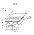
- Fig. 1 is an exploded perspective view of the three-electrode AC-type plasma display panel.
- the plasma display panel (hereinafter, abbreviated as "PDP") 100 is provided with a rear substrate 1 and a front substrate 2 which are arranged so as to be opposed to each other and a plurality of discharge chambers 16 which are formed between the substrates 1 and 2.
- Address electrodes 11 are formed on the inner face of the rear substrate 1 at predetermined intervals in a striped manner.
- a dielectric layer 19 is formed so as to cover the address electrodes 11.
- a partition (rib) 15 is formed in parallel with the address electrodes 11 on the upper face of the dielectric layer 19 between adjacent address electrodes 11.
- a fluorescent substance 17 is placed on the upper face of the dielectric layer 19 between adjacent partitions 15 and on the side face of the partition 15. The fluorescent substance 17 emits any one of red, green and blue fluorescence.
- a display electrode 12 (scanning electrode 12a and sustain electrode 12b) is formed on the inner face of the front substrate 2 at predetermined intervals in a striped manner.
- the display electrode 12 is constituted of a transparent conductive material such as ITO and arranged in a direction orthogonal to the address electrode 11.
- the intersecting point of the address electrode 11 and the display electrode 12 is given as a pixel of PDP 100.
- a dielectric layer 13 is formed so as to cover the display electrode 12, and a protective film 14 is formed so as to cover the dielectric layer 13.
- This protective film 14 protects the dielectric layer 13 from positive ions generated by plasmizing a discharge gas.
- This film is constituted of oxides of alkali earth metals such as MgO and SrO.
- the above-described rear substrate 1 and the front substrate 2 are laminated together to form discharge chambers 16 between the adjacent partitions 15.
- a discharge gas such as a mixed gas of Ne and Xe is sealed inside the discharge chambers 16.
- direct-current voltage is applied across the address electrode 11 and the scanning electrode 12a to cause a counter discharge.
- alternative-current voltage is applied across the scanning electrode 12a and the sustain electrode 12b to cause a surface discharge.
- the discharge gas sealed inside the discharge chambers 16 is plasmized, thereby irradiating vacuum ultraviolet light.
- the fluorescent substance 17 is excited by this ultraviolet light to emit visible light from the front substrate 2.
- Fig. 2 is a sectional view showing the peripheral edge portion of a plasma display panel.
- Projections 21 are formed at the peripheral edge of the rear substrate 1 in an architrave shape.
- a sealing material 20 containing a resin material is arranged between the leading end face of the projection 21 and the front substrate 2, thereby both substrates 1 and 2 are sealed.
- the sealing material 20 for example, thermo-setting resins such as epoxy resin and acrylic resin or ultraviolet light curing resins are employed.
- the sealing material 20 containing a resin material is employed, heating and cooling conditions are alleviated greatly during sealing of the panel, as compared with the case where a conventional sealing material composed of a low-melting point glass is employed.
- a sealing material may be employed which is obtained by mixing a low-melting point glass with a resin as a binder.
- impurity gases are released from the sealing material 20 containing a resin material.
- gases such as CO, H 2 and CH based gases are released from the sealing material 20 which is made up of epoxy resin or of acrylic resin.
- CO 2 , O 2 gas and others are released from the low-melting point glass, while H 2 O, CO 2 , CO gas and others are released from the acrylic resin.
- impurity gases such as H 2 O may intrude into a PDP from outside through the sealing material 20 after sealing.
- a getter (adsorption material) 22 which adsorbs an impurity gas is provided along the inner periphery of the sealing material 20.
- the getter 22 adsorbs water (H 2 O) oxygen (O 2 ) gas, carbon-based gases such as CO and CO 2 and others such as CH-based hydrocarbon gas.
- H 2 O water
- O 2 oxygen
- SrO formed in a sheet to give the thickness of about 150 ⁇ m may be employed as the getter 22.
- active metals such as Ba, Ca or Sr formed to give the thickness of 5 to 10 ⁇ m may be employed as the getter 22.
- a Zr-V-Fe-Ti -based material may also be employed as the getter 22.
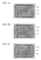
- Fig. 3A to Fig. 3C are plan views showing a plasma display panel equipped with a getter.
- the getter 22 is formed continuously along the inner whole periphery of the sealing material 20.
- it may be formed intermittently along the whole inner periphery of the sealing material 20.
- the getter 22 may be arranged on the surface of the rear substrate 1 on the inner side of the sealing material 20 or may be arranged on the surface of the front substrate 2.
- the thickness of the getter 22 may be thinner than that of the clearance between both the substrates 1 and 2 or may be equal to that of the clearance of the substrates 1 and 2.
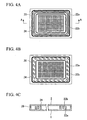
- Fig. 4A and Fig. 4B are plan views showing a plasma display panel equipped with a plurality of getters.
- a plurality of getters 22a and 22b may be arranged along the inner periphery of the sealing material 20 in a concentric manner.
- a plurality of the getters 22a and 22b may be formed continuously as shown in Fig. 4A , or they may be formed intermittently as shown in Fig. 4B . Further, among these plurality of getters, some of them are formed continuously, while the remaining getters may be formed intermittently.
- an impurity gas can be reliably adsorbed.
- Fig. 4C is a sectional view taken along the A-A line in Fig. 4A .
- some of the getters 22a may be loaded on the rear substrate 1, while the remaining getters 22b may be loaded on the front substrate 2.
- an impurity gas intrudes along a longer channel and also the getters 22a and 22b are arranged along the channel, thus making it possible to improve the adsorption efficiency of the impurity gas.
- all the plurality of the getters 22a and 22b may be loaded on the rear substrate 1 or all of them may be loaded on the front substrate 2.
- an ultraviolet shielding wall 24 is continuously installed along the inner periphery of the above-described getter 22.
- the ultraviolet shielding wall 24 prevents ultraviolet light generated in the discharge chamber 16 from being incident to the sealing material 20 and formed to give about 1 mm in width by an ultraviolet absorbing material such as PbO ⁇ B 2 O 3 ⁇ SiO 2 .
- the ultraviolet shielding wall 24 may be installed upright on the rear substrate 1 or may be installed upright on the front substrate 2.
- the height of the ultraviolet shielding wall 24 is formed equal to the clearance between the pair of substrates 1 and 2.
- the leading end of the ultraviolet shielding wall 24 installed upright on the rear substrate 1 is firmly attached to the front substrate 2.
- the above getter 22 is placed between the sealing material 20 and the ultraviolet shielding wall 24.
- an impurity gas released from the sealing material 20 can be blocked by the ultraviolet shielding wall 24 and securely adsorbed by the getter 22.
- the ultraviolet shielding wall 24 is constituted of the same ultraviolet absorbing material as that of the partition 15 and installed upright on the rear substrate 1 on which the partition 15 is installed. Thereby, as will be described later, the ultraviolet shielding wall 24 is formed simultaneously as the partition 15, thus making it possible to simplify the production steps and reduce the production cost.
- the partition 15 of the PDP prevents an erroneous discharge between adjacent discharge chambers 16 and formed to have a height equal to the clearance between the rear substrate 1 and the front substrate 2.
- the ultraviolet shielding wall 24 can be formed to have a height equal to a clearance between both the substrates 1 and 2. Thereby, ultraviolet light generated at the discharge chamber 16 can be securely prevented from being incident to the sealing material 20.
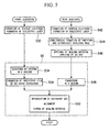
- Fig. 5 is a flow chart showing a method for producing the plasma display panel according to the present embodiment.
- a display electrode 12 and a dielectric layer 13 are formed on the inner face of the front substrate 2 shown in Fig. 2 (step 32).
- an address electrode 11 and a dielectric layer 19 are formed on the inner face of the rear substrate 1 (step 42).
- a partition 15 and an ultraviolet shielding wall 24 are formed simultaneously on the surface of a dielectric layer 19 of the rear substrate 1 (step 44).
- a film of ultraviolet absorbing material is first formed on the inner face of the rear substrate 1. More specifically, an ultraviolet absorbing material in paste form is applied to give the thickness of about 200 ⁇ m by a printing method or the like and dried to form the film.
- a dry film resist (DFR) is laminated on the surface of the film.
- the DFR is exposed and developed to provide a pattern along the configurations of the partition 15 and the ultraviolet shielding wall 24.
- sandblasting is performed using the DFR pattern as a mask, thereby giving a pattern to the film according to the configuration of the partition 15 and the ultraviolet shielding wall 24.
- the DFR is peeled and removed.
- the rear substrate 1 is put into a kiln to bake the partition 15 and the ultraviolet shielding wall 24. Therefore, the partition 15 and the ultraviolet shielding wall 24 are formed on the inner face of the rear substrate 1.
- a DFR is laminated on the inner face of the rear substrate 1.
- the DFR is exposed and developed to give a pattern according to the configurations of the partition 15 and the ultraviolet shielding wall 24.
- sandblasting is performed using the DFR pattern as a mask, thereby digging down into the rear substrate 1 composed of an ultraviolet absorbing material such as glass to a depth of about 150 ⁇ m.
- the DFR is peeled and removed. Therefore, the partition 15 and the ultraviolet shielding wall 24 are formed directly on the inner face of the rear substrate 1.
- the address electrode 11 and others are formed. Note that it is possible to form the partition 15 and the ultraviolet shielding wall 24 simultaneously with a method other than the above-described method.
- the inner side of adjacent partitions is coated with a fluorescent substance 17.
- the sealing material 20 and the getter 22 are arranged on the whole periphery of the rear substrate 1 (step 46).
- the sealing material 20 is arranged by applying a sealing material in paste form.
- the sealing material is applied by a droplet discharge method such as a dispenser method and an inkjet method or by a printing method.
- the getter 22 is arranged by laminating a SrO material sheet having the width of about 3 mm to 10 mm and the thickness of about 150 ⁇ m.
- the SrO material sheet can be formed by procedures in which SrO powder is placed into a mold, formed under a pressure of 200 to 400kgf/cm2 and further baked at about 1,200°C for about 30 minutes in a N 2 atmosphere.
- the front substrate 2 and the rear substrate 1 are put into a vacuum integrated process machine 50 to conduct the following steps up to a sealing step without exposure of the substrates 1 and 2 to an atmosphere.
- the rear substrate 1 is heated in a vacuum, thereby performing degassing treatment of the sealing material 20 containing a resin material and exhaust treatment (step 48).
- the sealing material 20 can be degassed and the getter 22 can be activated by this heating.
- the front substrate 2 is heated in a vacuum, thereby performing degassing treatment of a dielectric layer 13 and the like (step 34).
- a protective film 14 is formed on the inner face of the front substrate 2 by an electron beam (EB) vapor deposition or the like (step 36).
- EB electron beam
- an SrO-based material such as (SrCa)O has been studied as a constituent of the protective film 14 in place of a conventional material of MgO.
- the SrO-based material is much higher in hygroscopicity than MgO and has a feature that the color is changed upon absorption of moisture.
- the vacuum integrated process machine 50 performs steps from a degassing step of the substrates 1 and 2 to a sealing step of the substrates 1 and 2 via a forming step of the protective film 14, thus making it possible to prevent the change in color and rise in discharge voltage resulting from the moisture absorption of the protective film 14.
- both the substrates 1 and 2 are sealed (step 52). More specifically, these substrates 1 and 2 are first put into a chamber, and a discharge gas is introduced into the chamber. Next, the substrates 1 and 2 are in alignment (positioned) and temporarily fastened. Next, electric voltage is applied across the substrates 1 and 2 to perform aging discharge. Further, a driving voltage is applied across the electrodes of these substrates 1 and 2 to conduct a light emission test. As a result, the rear substrate 1 or the front substrate 2 which is found to be abnormal is removed, and the substrates 1 and 2 which are confirmed to normally emit light are fastened with each other.
- the sealing material 20 is constituted of an ultraviolet light curing resin
- the sealing material is cured by irradiating ultraviolet light to the sealing material 20.
- the sealing material 20 is cured by heating the sealing material 20.
- the inventor of the present application performed a moisture absorption test to the PDP according to the above embodiment and a conventional PDP, by which any change in discharge voltage was measured.
- the PDP according to the present embodiment was, as shown in Fig. 2 , provided with the getter 22 and the ultraviolet shielding wall 24. Specifically, a sheet-like substance obtained by baking SrO in N 2 gas as the getter 22 was employed. Further, PbO ⁇ B 2 O 3 ⁇ SiO 2 , which was the same material as that of the partition 15, was employed as a constituent of the ultraviolet shielding wall 24, and the ultraviolet shielding wall 24 was formed simultaneously with the partition 15. It is noted that an ultraviolet light curing resin was employed as the sealing material 20.
- a film composed of SrO ⁇ 20 mol% CaO with the thickness of 8000 Angstroms was formed as the protective film 14 by EB vapor deposition. Ne ⁇ 4% Xe gas was sealed as a discharge gas at 53.300 Pa (400 Torr).
- the conventional PDP was such that the getter 22 and the ultraviolet shielding wall 24 were removed from the PDP according to the present embodiment.
- Fig. 6A and Fig. 6B are graphs showing the results of the moisture absorption test of the PDPs. Specifically, Fig. 6A shows the results of the PDP according to the present embodiment, while Fig. 6B shows the results of the conventional PDP. It is noted that in the following graphs, a final cell turn on voltage means a driving voltage needed to start discharging all cells in a PDP which is composed of 300 cells arranged in two-dimensional matrix. Further, a first cell turn off voltage is a voltage at which the first cell is turned off when the driving voltage is gradually lowered from a state that all the cells are turned on.
- the inventor of the present application performed an aging test to the PDP according to the present embodiment and the conventional PDP, by which any change in discharge voltage was measured.
- a PDP in which a getter was removed was employed as the PDP according to the present embodiment.
- a PDP in which the ultraviolet shielding wall and the getter were removed was employed as the conventional PDP.
- the aging test was conducted by applying voltage to these PDPs for a long time at room temperature with a humidity of 50%, and the relationship between the aging time and the discharge sustain voltage was studied.
- Fig. 7A and 7B are graphs showing the results of the aging test of these PDPs. Specifically, Fig. 7A shows the results of the PDP according to the present embodiment, while Fig. 7B shows the results according to the conventional PDP.
- the discharge sustain voltage was increased with an increase in aging time and the final cell turn on voltage was increased by about 30V after 2000-hour of aging. This is considered to be due to the fact that ultraviolet light generated by discharge in the PDP kept entering a sealing material for a long time, by which a resin material contained in the sealing material decomposed and a CH-based impurity gas was released into the PDP, resulting in a decrease in purity of the discharge gas.
- the voltage was increased by less than 10V even after 2000-hour of aging. This is considered to be due to the fact that ultraviolet light generated by discharge in the PDP was absorbed by the ultraviolet shielding wall, thereby preventing an impurity gas from being released from the sealing material, resulting in a suppressed decrease of the purity of the discharge gas.
- the PDP according to the present embodiment is constituted so that getters are formed continuously or intermittently along the inner periphery of a sealing material.
- an impurity gas released from the sealing material or an impurity gas intruding through the sealing material are adsorbed by the getters, thus making it possible to suppress a decrease of the purity of a discharge gas sealed between a pair of substrates. Therefore, it is possible to suppress a rise of discharge voltage.
- an impurity gas can be adsorbed by the getters, it is possible to prevent the impurity gas from being adsorbed by a hygroscopic protective film.
- the PDP according to the present embodiment is constituted so as to have an ultraviolet light shielding wall formed continuously along the inner periphery of the sealing material. According to the above constitution, since ultraviolet light generated inside the sealing panel is absorbed by the ultraviolet shielding wall, the light is prevented from being incident to the sealing material. Thereby, it is possible to suppress the release of an impurity gas from the sealing material and suppress a rise of discharge voltage.
- the present invention is applied to a plasma display panel, but may be applied to a field emission display panel.
- the field emission display panel is such that electrons are emitted from an electron emitting source (emitter) arranged for every pixel into vacuum, and collided against a fluorescent substance, thereby attaining light emission.
- the field emission display panel includes a FED (Field Emission Display) equipped with a projection-like electron emitting element and a SED (Surface-Conduction Electron Emitter Display) equipped with a surface conductance-type electron emitting element.
- FED Field Emission Display
- SED Surface-Conduction Electron Emitter Display
- the present invention is applicable to a sealing panel.
Landscapes
- Engineering & Computer Science (AREA)
- Physics & Mathematics (AREA)
- Plasma & Fusion (AREA)
- Manufacturing & Machinery (AREA)
- Gas-Filled Discharge Tubes (AREA)
- Common Detailed Techniques For Electron Tubes Or Discharge Tubes (AREA)
Abstract
Description
- The present invention relates to a sealing panel.
- A plasma display panel is provided with a front substrate on which a sustain electrode and a scanning electrode are formed and a rear substrate on which an address electrode and a fluorescent substance are formed. Both of these substrates are fastened by a sealing material arranged at the peripheral edge and a discharge gas is sealed between the substrates.
When voltage is applied across these electrodes, the discharge gas is plasmized to emit ultraviolet light. The ultraviolet light is made incident to a fluorescent substance, thereby exciting the fluorescent substance to emit visible light. - Conventionally, a low-melting point glass was used as a sealing material for both of the substrates. However, in recent years, there has been proposed a technology in which resin materials are employed (refer to
Patent Document 1, for example). Employing resin materials allows wider heating and cooling conditions to be used in sealing panels, thus making it possible to greatly reduce the amount of time needed to produce panels.
DocumentJP 2005 005259 A
DocumentJP 2005 302586 A
Patent Document 1: Japanese Unexamined Patent Application, First Publication No.2002-75197 - However, when a resin material is employed as a sealing material, there is a concern that an impurity gas (such as water or carbon dioxide gas) may be released from the resin material into the panel. Further, when a mixture of a low-melting point glass with a resin material as a binder is used as a sealing material, there is a concern that an impurity gas may be released into the panel during sealing of the panel. Still further, there is a concern that after a panel is sealed, an impurity gas may make an intrusion into the panel through the sealing material from outside. In addition, when ultraviolet light generated inside the panel is made incident into the sealing material, the resin material may be decomposed to release an impurity gas (CH-based gas) into the panel. Thus, there is a problem that the purity of a discharge gas sealed inside the panel is lowered by these impurity gases, thereby raising the discharge voltage. The electric power consumption of a plasma display panel increases in association with a rise in discharge voltage.
Further, impurity gas released from a sealing material into the panel during sealing of the panel is adsorbed onto a film formed on the surface of a substrate. Thereby, the secondary electron emission coefficient of the surface of the substrate is lowered to raise the discharge voltage. When voltage is applied across the substrates for a predetermined time (initial aging treatment), the impurity gas is desorbed from the surfaces of the substrates, which stabilizes the discharge voltage. However, since the desorbed impurity gas remains between the substrates resulting in a decrease in the desorbing speed of the impurity gas, it is necessary to carry out a prolonged initial aging treatment. - The present invention has been made to solve the above problem, and has an object of providing a sealing panel capable of suppressing a rise in discharge voltage.
- In order to achieve the above-described object, the sealing panel according to the present invention is a sealing panel which includes: a pair of substrates, a sealing material which contains a resin material and is disposed on the whole periphery in a part between the pair of substrates; and a discharge gas which is sealed between the pair of substrates with the sealing material, an adsorption material which adsorbs an impurity gas released from the sealing material and an impurity gas passing through the sealing material, is formed continuously or intermittently along the inner periphery of the sealing material. An ultraviolet shielding wall which prevents ultraviolet light generated inside the sealing panel from being incident to the sealing material is formed continuously along the whole inner periphery of the sealing material.
It may be arranged such that the sealing material is a mixture of a glass material with a resin material as a binder.
According to the above constitution, an impurity gas released from the sealing material and an impurity gas that passes through the sealing material can be adsorbed by an adsorption material, thus making it possible to suppress a decrease of the purity of a discharge gas sealed between the pair of substrates and also making it possible to prevent an impurity gas from being adsorbed on the surface of the substrate. Therefore, it is possible to suppress a rise in discharge voltage.
In addition, it is possible to reduce the amount of time needed to conduct an initial aging treatment or eliminate the necessity of conducting the initial aging treatment. - Further, it may be arranged such that adsorption materials are provided on a plurality of peripheries in a concentric manner.
According to the above constitution, an impurity gas can be reliably adsorbed.
Further, it may be arranged such that some of the adsorption materials among the adsorption materials provided on a plurality of peripheries are loaded on one of a substrate of the pair the substrates; and the remaining adsorption materials among the adsorption materials installed on a plurality of peripheries are loaded on the other substrate of the pair of the substrates.
According to the above constitution, the impurity gas intrudes along a longer channel and also adsorption materials are arranged along the channel, thus making it possible to improve the adsorption efficiency of the impurity gas. - According to the above constitution, it is possible to prevent ultraviolet light generated inside the sealing panel from being incident to the sealing material. It is, thereby, possible to suppress the release of an impurity gas from the sealing material and suppress a rise in discharge voltage.
- It may be arranged such that the leading end of the ultraviolet shielding wall installed upright on a substrate of the pair of substrates is in contact with the other substrate of the pair of substrates.
According to the above constitution, it is possible to block an impurity gas released from the sealing material and an impurity gas intruding through the sealing material by the ultraviolet shielding wall and thereby suppress a decrease of the purity of a discharge gas. - It is desirable that the adsorption material is arranged between the sealing material and the ultraviolet shielding wall.
According to the above constitution, the adsorption materials can be used to securely adsorb an impurity gas blocked by the ultraviolet shielding wall. - Further, it is desirable that the sealing panel is a plasma display panel; and the ultraviolet shielding wall is constituted of the same material as that of a partition placed between pixels of the plasma display panel.
- According to the above constitution, it is possible to form the ultraviolet shielding wall at the same time with the partition, thereby simplifying production steps to reduce the production cost.
On the other hand, a method for producing the plasma display panel is a method for producing a plasma display panel which is provided with: a sealing material containing a resin material arranged on the whole periphery in a pair of substrates; and a discharge gas filled between the pair of substrates sealed with the sealing material, the method including: forming an ultraviolet shielding wall for preventing ultraviolet light generated inside the plasma display panel from being incident to the sealing material simultaneously with a partition placed between pixels of the plasma display panel.
A partition of the plasma display panel is to prevent an erroneous discharge between adjacent pixels and formed to have a height equal to a clearance of a pair of substrates. The partition is formed at the same time as the ultraviolet shielding wall, thus making it possible to form the ultraviolet shielding wall with a height which is equal to a clearance of the pair of substrates.
Thereby, it is possible to securely prevent ultraviolet light generated inside the plasma display panel from being incident to a sealing material. It is, therefore, possible to suppress the release of an impurity gas from the sealing material and also suppress a rise in discharge voltage. - According to the sealing panel of the present invention, it is possible to suppress a decrease of the purity of a discharge gas sealed between the pair of substrates. Further, an impurity gas can be prevented from being adsorbed on the surface of the substrate. Therefore, it is possible to suppress a rise in discharge voltage. In addition, it is possible to reduce the aging treatment time or eliminate the initial aging treatment.
-
-
Fig. 1 is an exploded perspective view of a three-electrode AC-type plasma display panel. -
Fig. 2 is a sectional view showing the peripheral edge portion of a plasma display panel. -
Fig. 3A is a plan view of a plasma display panel equipped with a getter. -
Fig. 3B is a plan view of a plasma display panel equipped with a getter. -
Fig. 3C is a plan view of a plasma display panel equipped with a getter. -
Fig. 4A is an explanatory view of a plasma display panel equipped with a plurality of getters. -
Fig. 4B is an explanatory view of a plasma display panel equipped with a plurality of getters. -
Fig. 4C is an explanatory view of a plasma display panel equipped with a plurality of getters. -
Fig. 5 is a flow chart covering a method producing a plasma display panel. -
Fig. 6A is a graph showing the results of a moisture absorption test of a plasma display panel. -
Fig. 6B is a graph showing the results of a moisture absorption test of a plasma display panel. -
Fig. 7A is a graph showing the results of an aging test of a plasma display panel. -
Fig. 7B is a graph showing the results of an aging test of a plasma display panel. -
- 1: rear substrate
- 2: front substrate
- 15: partition
- 16: discharge chamber
- 20: sealing material
- 22: getter (adsorption material)
- 24: ultraviolet shielding wall
- 100: plasma display panel (sealing panel)
- Hereinafter, embodiments according to the present invention will be explained with reference to the drawings. It is noted that in the individual drawings referred to in the following explanation, the scale of each member is adequately changed so that it can be drawn in a recognizable dimension.
In the present specification, the "inner face" of a substrate shall be the surface facing a surface of the other substrate which is paired with the substrate. -
Fig. 1 is an exploded perspective view of the three-electrode AC-type plasma display panel. The plasma display panel (hereinafter, abbreviated as "PDP") 100 is provided with arear substrate 1 and afront substrate 2 which are arranged so as to be opposed to each other and a plurality ofdischarge chambers 16 which are formed between thesubstrates -
Address electrodes 11 are formed on the inner face of therear substrate 1 at predetermined intervals in a striped manner. Adielectric layer 19 is formed so as to cover theaddress electrodes 11. Further, a partition (rib) 15 is formed in parallel with theaddress electrodes 11 on the upper face of thedielectric layer 19 betweenadjacent address electrodes 11. Still further, afluorescent substance 17 is placed on the upper face of thedielectric layer 19 betweenadjacent partitions 15 and on the side face of thepartition 15. Thefluorescent substance 17 emits any one of red, green and blue fluorescence. - On the other hand, a display electrode 12 (
scanning electrode 12a and sustainelectrode 12b) is formed on the inner face of thefront substrate 2 at predetermined intervals in a striped manner. Thedisplay electrode 12 is constituted of a transparent conductive material such as ITO and arranged in a direction orthogonal to theaddress electrode 11.
The intersecting point of theaddress electrode 11 and thedisplay electrode 12 is given as a pixel ofPDP 100. Further, adielectric layer 13 is formed so as to cover thedisplay electrode 12, and aprotective film 14 is formed so as to cover thedielectric layer 13. Thisprotective film 14 protects thedielectric layer 13 from positive ions generated by plasmizing a discharge gas. This film is constituted of oxides of alkali earth metals such as MgO and SrO. - The above-described
rear substrate 1 and thefront substrate 2 are laminated together to formdischarge chambers 16 between theadjacent partitions 15. A discharge gas such as a mixed gas of Ne and Xe is sealed inside thedischarge chambers 16.
Then, direct-current voltage is applied across theaddress electrode 11 and thescanning electrode 12a to cause a counter discharge. Further, alternative-current voltage is applied across thescanning electrode 12a and the sustainelectrode 12b to cause a surface discharge. Then, the discharge gas sealed inside thedischarge chambers 16 is plasmized, thereby irradiating vacuum ultraviolet light. Thefluorescent substance 17 is excited by this ultraviolet light to emit visible light from thefront substrate 2. -
Fig. 2 is a sectional view showing the peripheral edge portion of a plasma display panel.Projections 21 are formed at the peripheral edge of therear substrate 1 in an architrave shape. A sealingmaterial 20 containing a resin material is arranged between the leading end face of theprojection 21 and thefront substrate 2, thereby bothsubstrates material 20, for example, thermo-setting resins such as epoxy resin and acrylic resin or ultraviolet light curing resins are employed. As described above, when the sealingmaterial 20 containing a resin material is employed, heating and cooling conditions are alleviated greatly during sealing of the panel, as compared with the case where a conventional sealing material composed of a low-melting point glass is employed. Thus, it is possible to greatly reduce the amount of time needed to produce the panel. It is noted that a sealing material may be employed which is obtained by mixing a low-melting point glass with a resin as a binder. - Incidentally, during sealing the
substrates material 20 containing a resin material. In addition to H2O and CO2, for example, gases such as CO, H2 and CH based gases are released from the sealingmaterial 20 which is made up of epoxy resin or of acrylic resin. Further, in the case of a sealing material obtained by mixing a low-melting point glass with acrylic resin, CO2, O2 gas and others are released from the low-melting point glass, while H2O, CO2, CO gas and others are released from the acrylic resin. Further, there is a concern that impurity gases such as H2O may intrude into a PDP from outside through the sealingmaterial 20 after sealing. - Thus, a getter (adsorption material) 22 which adsorbs an impurity gas is provided along the inner periphery of the sealing
material 20. Thegetter 22 adsorbs water (H2O) oxygen (O2) gas, carbon-based gases such as CO and CO2 and others such as CH-based hydrocarbon gas. Specifically, SrO formed in a sheet to give the thickness of about 150 µm may be employed as thegetter 22. Further, active metals such as Ba, Ca or Sr formed to give the thickness of 5 to 10 µm may be employed as thegetter 22. A Zr-V-Fe-Ti -based material may also be employed as thegetter 22. -
Fig. 3A to Fig. 3C are plan views showing a plasma display panel equipped with a getter.
As shown inFig. 3A , it is desirable that thegetter 22 is formed continuously along the inner whole periphery of the sealingmaterial 20. As shown inFig. 3B and Fig. 3C , it may be formed intermittently along the whole inner periphery of the sealingmaterial 20.
It is noted that, as shown inFig. 2 , thegetter 22 may be arranged on the surface of therear substrate 1 on the inner side of the sealingmaterial 20 or may be arranged on the surface of thefront substrate 2. Further, as shown inFig. 2 , the thickness of thegetter 22 may be thinner than that of the clearance between both thesubstrates substrates -
Fig. 4A and Fig. 4B are plan views showing a plasma display panel equipped with a plurality of getters. As shown inFig. 4A , a plurality ofgetters material 20 in a concentric manner. A plurality of thegetters Fig. 4A , or they may be formed intermittently as shown inFig. 4B . Further, among these plurality of getters, some of them are formed continuously, while the remaining getters may be formed intermittently. As described so far, by arranging a plurality of thegetters -
Fig. 4C is a sectional view taken along the A-A line inFig. 4A . As shown inFig. 4C , among a plurality of thegetters getters 22a may be loaded on therear substrate 1, while the remaininggetters 22b may be loaded on thefront substrate 2. Thereby, an impurity gas intrudes along a longer channel and also thegetters getters rear substrate 1 or all of them may be loaded on thefront substrate 2. - Reverting to
Fig. 2 , anultraviolet shielding wall 24 is continuously installed along the inner periphery of the above-describedgetter 22. Theultraviolet shielding wall 24 prevents ultraviolet light generated in thedischarge chamber 16 from being incident to the sealingmaterial 20 and formed to give about 1 mm in width by an ultraviolet absorbing material such as PbO·B2O3·SiO2. As shown inFig. 2 , theultraviolet shielding wall 24 may be installed upright on therear substrate 1 or may be installed upright on thefront substrate 2. - The height of the
ultraviolet shielding wall 24 is formed equal to the clearance between the pair ofsubstrates ultraviolet shielding wall 24 installed upright on therear substrate 1 is firmly attached to thefront substrate 2. According to the above constitution, it is possible to block an impurity gas released from the sealingmaterial 20 and an impurity gas intruding through the sealingmaterial 20 by the ultraviolet shielding wall. It is desirable that theabove getter 22 is placed between the sealingmaterial 20 and theultraviolet shielding wall 24.
According to the above constitution, an impurity gas released from the sealingmaterial 20 can be blocked by theultraviolet shielding wall 24 and securely adsorbed by thegetter 22. - It is desirable that the
ultraviolet shielding wall 24 is constituted of the same ultraviolet absorbing material as that of thepartition 15 and installed upright on therear substrate 1 on which thepartition 15 is installed. Thereby, as will be described later, theultraviolet shielding wall 24 is formed simultaneously as thepartition 15, thus making it possible to simplify the production steps and reduce the production cost.
Incidentally, thepartition 15 of the PDP prevents an erroneous discharge betweenadjacent discharge chambers 16 and formed to have a height equal to the clearance between therear substrate 1 and thefront substrate 2. By forming thepartition 15 simultaneously with theultraviolet shielding wall 24, theultraviolet shielding wall 24 can be formed to have a height equal to a clearance between both thesubstrates discharge chamber 16 can be securely prevented from being incident to the sealingmaterial 20. - Next, a method for producing the plasma display panel according to the present embodiment will be explained with reference to
Fig. 2 andFig. 5. Fig. 5 is a flow chart showing a method for producing the plasma display panel according to the present embodiment.
First, adisplay electrode 12 and adielectric layer 13 are formed on the inner face of thefront substrate 2 shown inFig. 2 (step 32). Further, anaddress electrode 11 and adielectric layer 19 are formed on the inner face of the rear substrate 1 (step 42). - Next, a
partition 15 and anultraviolet shielding wall 24 are formed simultaneously on the surface of adielectric layer 19 of the rear substrate 1 (step 44). Specifically, a film of ultraviolet absorbing material is first formed on the inner face of therear substrate 1. More specifically, an ultraviolet absorbing material in paste form is applied to give the thickness of about 200 µm by a printing method or the like and dried to form the film. Next, a dry film resist (DFR) is laminated on the surface of the film. Next, the DFR is exposed and developed to provide a pattern along the configurations of thepartition 15 and theultraviolet shielding wall 24. Next, sandblasting is performed using the DFR pattern as a mask, thereby giving a pattern to the film according to the configuration of thepartition 15 and theultraviolet shielding wall 24. Next, the DFR is peeled and removed. Therear substrate 1 is put into a kiln to bake thepartition 15 and theultraviolet shielding wall 24. Therefore, thepartition 15 and theultraviolet shielding wall 24 are formed on the inner face of therear substrate 1. - As another method for forming them simultaneously, there is a method in which before the
address electrode 11 and thedielectric layer 19 are formed, a DFR is laminated on the inner face of therear substrate 1. Next, the DFR is exposed and developed to give a pattern according to the configurations of thepartition 15 and theultraviolet shielding wall 24. Next, sandblasting is performed using the DFR pattern as a mask, thereby digging down into therear substrate 1 composed of an ultraviolet absorbing material such as glass to a depth of about 150 µm. Next, the DFR is peeled and removed. Therefore, thepartition 15 and theultraviolet shielding wall 24 are formed directly on the inner face of therear substrate 1. Thereafter, theaddress electrode 11 and others are formed. Note that it is possible to form thepartition 15 and theultraviolet shielding wall 24 simultaneously with a method other than the above-described method.
Next, the inner side of adjacent partitions is coated with afluorescent substance 17. - Next, the sealing
material 20 and thegetter 22 are arranged on the whole periphery of the rear substrate 1 (step 46). The sealingmaterial 20 is arranged by applying a sealing material in paste form. The sealing material is applied by a droplet discharge method such as a dispenser method and an inkjet method or by a printing method. Further, thegetter 22 is arranged by laminating a SrO material sheet having the width of about 3 mm to 10 mm and the thickness of about 150 µm. The SrO material sheet can be formed by procedures in which SrO powder is placed into a mold, formed under a pressure of 200 to 400kgf/cm2 and further baked at about 1,200°C for about 30 minutes in a N2 atmosphere. - Next, the
front substrate 2 and therear substrate 1 are put into a vacuum integratedprocess machine 50 to conduct the following steps up to a sealing step without exposure of thesubstrates
First, therear substrate 1 is heated in a vacuum, thereby performing degassing treatment of the sealingmaterial 20 containing a resin material and exhaust treatment (step 48). The sealingmaterial 20 can be degassed and thegetter 22 can be activated by this heating. Further, thefront substrate 2 is heated in a vacuum, thereby performing degassing treatment of adielectric layer 13 and the like (step 34). Next, aprotective film 14 is formed on the inner face of thefront substrate 2 by an electron beam (EB) vapor deposition or the like (step 36). - In recent years, in order to reduce the electric power consumption of a PDP, an SrO-based material such as (SrCa)O has been studied as a constituent of the
protective film 14 in place of a conventional material of MgO. The SrO-based material is much higher in hygroscopicity than MgO and has a feature that the color is changed upon absorption of moisture. In this respect, the vacuum integratedprocess machine 50 performs steps from a degassing step of thesubstrates substrates protective film 14, thus making it possible to prevent the change in color and rise in discharge voltage resulting from the moisture absorption of theprotective film 14. - Next, both the
substrates substrates substrates substrates substrates rear substrate 1 or thefront substrate 2 which is found to be abnormal is removed, and thesubstrates material 20 is constituted of an ultraviolet light curing resin, the sealing material is cured by irradiating ultraviolet light to the sealingmaterial 20. Further, in the case where the sealingmaterial 20 is constituted of a thermo-setting resin, the sealingmaterial 20 is cured by heating the sealingmaterial 20.
Thus, thesesubstrates substrates - The inventor of the present application performed a moisture absorption test to the PDP according to the above embodiment and a conventional PDP, by which any change in discharge voltage was measured. The PDP according to the present embodiment was, as shown in
Fig. 2 , provided with thegetter 22 and theultraviolet shielding wall 24. Specifically, a sheet-like substance obtained by baking SrO in N2 gas as thegetter 22 was employed. Further, PbO· B2O3· SiO2, which was the same material as that of thepartition 15, was employed as a constituent of theultraviolet shielding wall 24, and theultraviolet shielding wall 24 was formed simultaneously with thepartition 15. It is noted that an ultraviolet light curing resin was employed as the sealingmaterial 20. Further, a film composed of SrO·20 mol% CaO with the thickness of 8000 Angstroms was formed as theprotective film 14 by EB vapor deposition. Ne·4% Xe gas was sealed as a discharge gas at 53.300 Pa (400 Torr).
On the other hand, the conventional PDP was such that thegetter 22 and theultraviolet shielding wall 24 were removed from the PDP according to the present embodiment. - The moisture absorption test was conducted by placing these PDPs to stand in a thermostatic chamber at a constant temperature of 85°C and the humidity of 95%. Next, the relationship between the standing time and the discharge sustain voltage was studied.
Fig. 6A and Fig. 6B are graphs showing the results of the moisture absorption test of the PDPs. Specifically,Fig. 6A shows the results of the PDP according to the present embodiment, whileFig. 6B shows the results of the conventional PDP. It is noted that in the following graphs, a final cell turn on voltage means a driving voltage needed to start discharging all cells in a PDP which is composed of 300 cells arranged in two-dimensional matrix. Further, a first cell turn off voltage is a voltage at which the first cell is turned off when the driving voltage is gradually lowered from a state that all the cells are turned on. - In the case of the conventional PDP shown in
Fig. 6B , there was found a great increase in the first cell turn off voltage and the final cell turn on voltage after a short time standing in the chamber. This is considered to be due to the fact that water inside the thermostatic chamber passed through the sealing material and intruded into the PDP, resulting in a decrease in the purity of a discharge gas.
On the other hand, in the case of the PDP according to the present embodiment shown inFig. 6A , variations in voltage was within 5V even after a long time standing in the chamber, and the results of the test were practically acceptable. This is considered to be due to the fact that water passed through the sealing material and intruded into the PDP, but the water was adsorbed by a getter, thereby suppressing the decrease of the purity of the discharge gas. - Further, the inventor of the present application performed an aging test to the PDP according to the present embodiment and the conventional PDP, by which any change in discharge voltage was measured. In order to confirm the effect of the ultraviolet shielding wall, a PDP in which a getter was removed was employed as the PDP according to the present embodiment. Further, a PDP in which the ultraviolet shielding wall and the getter were removed was employed as the conventional PDP.
The aging test was conducted by applying voltage to these PDPs for a long time at room temperature with a humidity of 50%, and the relationship between the aging time and the discharge sustain voltage was studied. -
Fig. 7A and 7B are graphs showing the results of the aging test of these PDPs. Specifically,Fig. 7A shows the results of the PDP according to the present embodiment, whileFig. 7B shows the results according to the conventional PDP.
In the case of the conventional PDP shown inFig. 7B , the discharge sustain voltage was increased with an increase in aging time and the final cell turn on voltage was increased by about 30V after 2000-hour of aging. This is considered to be due to the fact that ultraviolet light generated by discharge in the PDP kept entering a sealing material for a long time, by which a resin material contained in the sealing material decomposed and a CH-based impurity gas was released into the PDP, resulting in a decrease in purity of the discharge gas. - On the other hand, in the case of the PDP according to the present embodiment shown in
Fig. 7A , the voltage was increased by less than 10V even after 2000-hour of aging. This is considered to be due to the fact that ultraviolet light generated by discharge in the PDP was absorbed by the ultraviolet shielding wall, thereby preventing an impurity gas from being released from the sealing material, resulting in a suppressed decrease of the purity of the discharge gas. - As described above in detail, the PDP according to the present embodiment is constituted so that getters are formed continuously or intermittently along the inner periphery of a sealing material. According to the above constitution, an impurity gas released from the sealing material or an impurity gas intruding through the sealing material are adsorbed by the getters, thus making it possible to suppress a decrease of the purity of a discharge gas sealed between a pair of substrates. Therefore, it is possible to suppress a rise of discharge voltage.
Further, since an impurity gas can be adsorbed by the getters, it is possible to prevent the impurity gas from being adsorbed by a hygroscopic protective film. Thereby, it is possible to suppress the decrease of the secondary electron emission coefficient on the surface of a substrate and also suppress the rise of discharge voltage. Further, it is possible to adsorb with the getters an impurity gas desorbed from the protective film upon application of voltage across the substrates for a predetermined amount of time (initial aging treatment) without remaining between the substrates. Thereby, the impurity gas can be desorbed completely and quickly. As a result, the initial aging time can be reduced. - Further, the PDP according to the present embodiment is constituted so as to have an ultraviolet light shielding wall formed continuously along the inner periphery of the sealing material. According to the above constitution, since ultraviolet light generated inside the sealing panel is absorbed by the ultraviolet shielding wall, the light is prevented from being incident to the sealing material. Thereby, it is possible to suppress the release of an impurity gas from the sealing material and suppress a rise of discharge voltage.
- The present invention shall not be limited in technical scope to the above described individual embodiments but may include any modifications of the above embodiments within a scope not departing from the present invention as defined in the appended claims.
In other words, specific materials and constitutions described in the above embodiments are only examples and may be modified, whenever necessary. - For example, in the above embodiment, the present invention is applied to a plasma display panel, but may be applied to a field emission display panel. The field emission display panel is such that electrons are emitted from an electron emitting source (emitter) arranged for every pixel into vacuum, and collided against a fluorescent substance, thereby attaining light emission. Specifically, the field emission display panel includes a FED (Field Emission Display) equipped with a projection-like electron emitting element and a SED (Surface-Conduction Electron Emitter Display) equipped with a surface conductance-type electron emitting element. In a case where the present invention is applied to the field emission display panel, it is also possible to suppress a rise of discharge voltage.
- The present invention is applicable to a sealing panel.
Claims (7)
- A sealing panel (100) comprising: a pair of substrates (1, 2);
a sealing material (20) which contains a resin material and is disposed on the whole periphery in a part between the pair of substrates (1, 2); and
a discharge gas which is sealed between the pair of substrates (1, 2) with the sealing material (20), wherein
an adsorption material (22) adapted to adsorb an impurity gas released from the sealing material (20) and an impurity gas passing through the sealing material (20), is formed continuously or intermittently along the inner periphery of the sealing material (20), characterized in that
an ultraviolet shielding wall (24) adapted to prevent ultraviolet light generated inside the sealing panel (100) from being incident to the sealing material (20) is formed continuously along the whole inner periphery of the sealing material (20). - The sealing panel (100) according to claim 1, wherein the sealing material (20) is a mixture of a glass material with a resin material as a binder.
- The sealing panel (100) according to claim 1, wherein adsorption materials (22a, 22b) are provided on a plurality of peripheries in a concentric manner.
- The sealing panel (100) according to claim 3, wherein,
some of the adsorption materials among the adsorption materials (22a, 22b) provided on a plurality of peripheries are loaded on one of a substrate of the pair the substrates (1, 2); and
the remaining adsorption materials among the adsorption materials (22a, 22b) installed on a plurality of peripheries are loaded on the other substrate of the pair of the substrates (1, 2). - The sealing panel (100) according to claim 1, wherein the leading end of the ultraviolet shielding wall (24) installed upright on a substrate of the pair of substrates (1, 2) is in contact with the other substrate of the pair of substrates (1, 2).
- The sealing panel (100) according to claim 1, wherein the adsorption material (22) is arranged between the sealing material (20) and the ultraviolet shielding wall (24).
- The sealing panel (100) according to claim 1, wherein
the sealing panel (100) is a plasma display panel; and
the ultraviolet shielding wall (24) is constituted of the same material as that of a partition placed between pixels of the plasma display panel.
Applications Claiming Priority (2)
| Application Number | Priority Date | Filing Date | Title |
|---|---|---|---|
| JP2006107547A JP4787054B2 (en) | 2006-04-10 | 2006-04-10 | Sealing panel and plasma display panel manufacturing method |
| PCT/JP2007/057561 WO2007119676A1 (en) | 2006-04-10 | 2007-04-04 | Method for manufacturing sealing panel and plasma display panel |
Publications (3)
| Publication Number | Publication Date |
|---|---|
| EP2009667A1 EP2009667A1 (en) | 2008-12-31 |
| EP2009667A4 EP2009667A4 (en) | 2011-03-02 |
| EP2009667B1 true EP2009667B1 (en) | 2012-06-13 |
Family
ID=38609435
Family Applications (1)
| Application Number | Title | Priority Date | Filing Date |
|---|---|---|---|
| EP07740997A Expired - Fee Related EP2009667B1 (en) | 2006-04-10 | 2007-04-04 | Sealing panel and method for producing plasma display panel |
Country Status (6)
| Country | Link |
|---|---|
| EP (1) | EP2009667B1 (en) |
| JP (1) | JP4787054B2 (en) |
| KR (2) | KR101042036B1 (en) |
| CN (1) | CN101421813B (en) |
| RU (1) | RU2395863C2 (en) |
| WO (1) | WO2007119676A1 (en) |
Families Citing this family (4)
| Publication number | Priority date | Publication date | Assignee | Title |
|---|---|---|---|---|
| JP5173444B2 (en) * | 2008-01-07 | 2013-04-03 | 株式会社アルバック | Sealing panel manufacturing method and plasma display panel manufacturing method using the same |
| JP5173504B2 (en) * | 2008-03-17 | 2013-04-03 | 株式会社アルバック | Sealing panel manufacturing method and plasma display panel manufacturing method using the same |
| JP2012084480A (en) * | 2010-10-14 | 2012-04-26 | Panasonic Corp | Plasma display panel and manufacturing method therefor |
| WO2018062069A1 (en) | 2016-09-30 | 2018-04-05 | パナソニックIpマネジメント株式会社 | Method for producing glass panel unit, and method for producing glass window |
Family Cites Families (17)
| Publication number | Priority date | Publication date | Assignee | Title |
|---|---|---|---|---|
| IT1295366B1 (en) * | 1997-10-20 | 1999-05-12 | Getters Spa | GETTER SYSTEM FOR PLASMA FLAT PANELS USED AS SCREENS |
| KR20000000549A (en) * | 1998-06-01 | 2000-01-15 | 구자홍 | Getter structure of a gas discharge display device |
| JP4579487B2 (en) * | 1998-09-14 | 2010-11-10 | パナソニック株式会社 | Method for manufacturing gas discharge panel |
| JP3569458B2 (en) * | 1999-03-26 | 2004-09-22 | パイオニア株式会社 | Plasma display panel |
| FR2793950A1 (en) * | 1999-05-21 | 2000-11-24 | Thomson Plasma | METHOD FOR MANUFACTURING COMPONENTS ON GLASS SUBSTRATES TO BE SEALED, SUCH AS FLAT DISPLAYS OF THE PLASMA PANEL TYPE |
| US6479944B2 (en) | 2000-07-25 | 2002-11-12 | Lg Electronics Inc. | Plasma display panel, fabrication apparatus for the same, and fabrication process thereof |
| JP2002358892A (en) * | 2001-05-30 | 2002-12-13 | Matsushita Electric Ind Co Ltd | Gas discharge display panel and its manufacturing method |
| JP3962832B2 (en) * | 2002-03-22 | 2007-08-22 | 株式会社日立プラズマパテントライセンシング | Method and apparatus for manufacturing substrate structure for plasma display panel |
| JP2005005259A (en) * | 2003-05-19 | 2005-01-06 | Matsushita Electric Ind Co Ltd | Plasma display panel |
| TWI239548B (en) * | 2003-11-11 | 2005-09-11 | Au Optronics Corp | Plasma display panel |
| CN1545123A (en) * | 2003-11-21 | 2004-11-10 | 友达光电股份有限公司 | Plasma display unit |
| JP2005302586A (en) * | 2004-04-14 | 2005-10-27 | Matsushita Electric Ind Co Ltd | Plasma display panel |
| JP2005314136A (en) * | 2004-04-27 | 2005-11-10 | Matsushita Electric Ind Co Ltd | Sealing material for air tightly sealing and glass paste composition |
| CN101040361B (en) * | 2004-08-17 | 2011-03-30 | 松下电器产业株式会社 | Plasma display panel and method for manufacturing same |
| JPWO2006033380A1 (en) * | 2004-09-24 | 2008-05-15 | 旭硝子株式会社 | SEALING MATERIAL COMPOSITION, HERMETIC CONTAINER USING THE SAME, ELECTRONIC COMPONENT OVERCOAT AND METHOD FOR PRODUCING THEM |
| JP4234662B2 (en) | 2004-09-30 | 2009-03-04 | 株式会社東芝 | Electronic device and data recording method thereof |
| JP4176737B2 (en) * | 2005-05-09 | 2008-11-05 | パイオニア株式会社 | Plasma display panel |
-
2006
- 2006-04-10 JP JP2006107547A patent/JP4787054B2/en not_active Expired - Fee Related
-
2007
- 2007-04-04 CN CN2007800127176A patent/CN101421813B/en not_active Expired - Fee Related
- 2007-04-04 WO PCT/JP2007/057561 patent/WO2007119676A1/en active Application Filing
- 2007-04-04 KR KR1020087024645A patent/KR101042036B1/en active IP Right Grant
- 2007-04-04 EP EP07740997A patent/EP2009667B1/en not_active Expired - Fee Related
- 2007-04-04 RU RU2008139894/09A patent/RU2395863C2/en not_active IP Right Cessation
- 2007-04-04 KR KR1020107023382A patent/KR20100116716A/en not_active Application Discontinuation
Also Published As
| Publication number | Publication date |
|---|---|
| EP2009667A4 (en) | 2011-03-02 |
| EP2009667A1 (en) | 2008-12-31 |
| JP2007280838A (en) | 2007-10-25 |
| JP4787054B2 (en) | 2011-10-05 |
| KR20100116716A (en) | 2010-11-01 |
| KR20080110612A (en) | 2008-12-18 |
| RU2395863C2 (en) | 2010-07-27 |
| CN101421813B (en) | 2012-05-30 |
| CN101421813A (en) | 2009-04-29 |
| KR101042036B1 (en) | 2011-06-16 |
| WO2007119676A1 (en) | 2007-10-25 |
| RU2008139894A (en) | 2010-04-20 |
Similar Documents
| Publication | Publication Date | Title |
|---|---|---|
| WO2005088668A1 (en) | Plasma display panel | |
| EP2009667B1 (en) | Sealing panel and method for producing plasma display panel | |
| KR100723752B1 (en) | Production method for plasma display panel excellent in luminous characteristics | |
| US7518232B2 (en) | Plasma display panel | |
| EP1769519B1 (en) | Process for the production of plasma displays with distributed getter material and displays thus obtained | |
| KR100723751B1 (en) | Discharge light-emitting device and method of manufacture thereof | |
| JP3366895B2 (en) | Method for manufacturing plasma display panel | |
| RU2435246C2 (en) | Method and device for manufacturing of sealed panel and method and device for manufacturing of plasma display panel | |
| US20050099122A1 (en) | Plasma display panel structure | |
| JP2002367520A (en) | Plasma display panel and its manufacturing method | |
| JP2003109503A (en) | Manufacturing method of plasma display panel | |
| US7304431B2 (en) | Plasma display panel | |
| JP2008130407A (en) | Plasma display panel, method of manufacturing plasma display panel, and film forming device | |
| KR100867506B1 (en) | Plasma display panel | |
| JP5325812B2 (en) | Method for manufacturing plasma display panel | |
| JP5654405B2 (en) | Method for manufacturing plasma display panel | |
| JP4760178B2 (en) | Plasma display panel | |
| JP2011222325A (en) | Method for manufacturing plasma display panel, and plasma display panel | |
| WO2009107217A1 (en) | Plasma display panel | |
| JP2008287966A (en) | Plasma display panel | |
| JP2009266717A (en) | Method of manufacturing plasma display panel | |
| JP2010129302A (en) | Plasma display panel and method for manufacturing same | |
| JP2012209157A (en) | Plasma display panel and manufacturing method of the same | |
| KR20090010892A (en) | Methods for manufature of plasma display panel and plasma display panel | |
| JP2002117765A (en) | Method for manufacturing image display device, and image display device manufactured by using it |
Legal Events
| Date | Code | Title | Description |
|---|---|---|---|
| PUAI | Public reference made under article 153(3) epc to a published international application that has entered the european phase |
Free format text: ORIGINAL CODE: 0009012 |
|
| 17P | Request for examination filed |
Effective date: 20081110 |
|
| AK | Designated contracting states |
Kind code of ref document: A1 Designated state(s): AT BE BG CH CY CZ DE DK EE ES FI FR GB GR HU IE IS IT LI LT LU LV MC MT NL PL PT RO SE SI SK TR |
|
| AX | Request for extension of the european patent |
Extension state: AL BA HR MK RS |
|
| DAX | Request for extension of the european patent (deleted) | ||
| RBV | Designated contracting states (corrected) |
Designated state(s): IT |
|
| REG | Reference to a national code |
Ref country code: DE Ref legal event code: 8566 |
|
| A4 | Supplementary search report drawn up and despatched |
Effective date: 20110202 |
|
| RIC1 | Information provided on ipc code assigned before grant |
Ipc: H01J 17/18 20060101ALI20110125BHEP Ipc: H01J 9/26 20060101ALI20110125BHEP Ipc: H01J 9/24 20060101ALI20110125BHEP Ipc: H01J 17/49 20060101ALI20110125BHEP Ipc: H01J 17/24 20060101AFI20110125BHEP |
|
| REG | Reference to a national code |
Ref country code: DE Ref legal event code: R079 Free format text: PREVIOUS MAIN CLASS: H01J0005200000 Ipc: H01J0017240000 |
|
| GRAP | Despatch of communication of intention to grant a patent |
Free format text: ORIGINAL CODE: EPIDOSNIGR1 |
|
| RIC1 | Information provided on ipc code assigned before grant |
Ipc: H01J 9/26 20060101ALI20120111BHEP Ipc: H01J 17/24 20120101AFI20120111BHEP Ipc: H01J 17/49 20120101ALI20120111BHEP Ipc: H01J 9/24 20060101ALI20120111BHEP Ipc: H01J 17/18 20120101ALI20120111BHEP |
|
| RTI1 | Title (correction) |
Free format text: SEALING PANEL AND METHOD FOR PRODUCING PLASMA DISPLAY PANEL |
|
| GRAS | Grant fee paid |
Free format text: ORIGINAL CODE: EPIDOSNIGR3 |
|
| RIN1 | Information on inventor provided before grant (corrected) |
Inventor name: IIJIMA, EIICHI Inventor name: KURAUCHI, TOSHIHARU |
|
| GRAA | (expected) grant |
Free format text: ORIGINAL CODE: 0009210 |
|
| RAP1 | Party data changed (applicant data changed or rights of an application transferred) |
Owner name: ULVAC, INC. |
|
| AK | Designated contracting states |
Kind code of ref document: B1 Designated state(s): IT |
|
| PLBE | No opposition filed within time limit |
Free format text: ORIGINAL CODE: 0009261 |
|
| STAA | Information on the status of an ep patent application or granted ep patent |
Free format text: STATUS: NO OPPOSITION FILED WITHIN TIME LIMIT |
|
| 26N | No opposition filed |
Effective date: 20130314 |
|
| PGFP | Annual fee paid to national office [announced via postgrant information from national office to epo] |
Ref country code: IT Payment date: 20190429 Year of fee payment: 13 |
|
| PG25 | Lapsed in a contracting state [announced via postgrant information from national office to epo] |
Ref country code: IT Free format text: LAPSE BECAUSE OF NON-PAYMENT OF DUE FEES Effective date: 20200404 |