EP2003778A2 - Berührungsschalter - Google Patents
Berührungsschalter Download PDFInfo
- Publication number
- EP2003778A2 EP2003778A2 EP08010057A EP08010057A EP2003778A2 EP 2003778 A2 EP2003778 A2 EP 2003778A2 EP 08010057 A EP08010057 A EP 08010057A EP 08010057 A EP08010057 A EP 08010057A EP 2003778 A2 EP2003778 A2 EP 2003778A2
- Authority
- EP
- European Patent Office
- Prior art keywords
- substrate
- conductive
- light
- touch switch
- conductive member
- Prior art date
- Legal status (The legal status is an assumption and is not a legal conclusion. Google has not performed a legal analysis and makes no representation as to the accuracy of the status listed.)
- Granted
Links
Images
Classifications
-
- H—ELECTRICITY
- H03—ELECTRONIC CIRCUITRY
- H03K—PULSE TECHNIQUE
- H03K17/00—Electronic switching or gating, i.e. not by contact-making and –breaking
- H03K17/94—Electronic switching or gating, i.e. not by contact-making and –breaking characterised by the way in which the control signals are generated
- H03K17/96—Touch switches
- H03K17/962—Capacitive touch switches
-
- H—ELECTRICITY
- H01—ELECTRIC ELEMENTS
- H01H—ELECTRIC SWITCHES; RELAYS; SELECTORS; EMERGENCY PROTECTIVE DEVICES
- H01H9/00—Details of switching devices, not covered by groups H01H1/00 - H01H7/00
- H01H9/16—Indicators for switching condition, e.g. "on" or "off"
-
- H—ELECTRICITY
- H01—ELECTRIC ELEMENTS
- H01H—ELECTRIC SWITCHES; RELAYS; SELECTORS; EMERGENCY PROTECTIVE DEVICES
- H01H9/00—Details of switching devices, not covered by groups H01H1/00 - H01H7/00
- H01H9/18—Distinguishing marks on switches, e.g. for indicating switch location in the dark; Adaptation of switches to receive distinguishing marks
- H01H9/182—Illumination of the symbols or distinguishing marks
-
- H—ELECTRICITY
- H01—ELECTRIC ELEMENTS
- H01H—ELECTRIC SWITCHES; RELAYS; SELECTORS; EMERGENCY PROTECTIVE DEVICES
- H01H2219/00—Legends
- H01H2219/054—Optical elements
- H01H2219/064—Optical isolation of switch sites
Definitions
- the present invention relates to a configuration of an electrostatic capacity type touch switch designed to detect a touch operation of an operator on the basis of a variation of the electrostatic capacity between electrodes, and more particularly to a configuration of a touch switch suitable for use in a control panel for devices in the interior of an automobile.
- the electrode member functions as an electrostatic capacity sensor so as to read a variation in impedance (electrostatic capacity) of the electrode when the human body comes into contact with the electrode, thereby detecting the on/off-state of the touch switch.
- the electrode member is made of a metallic plate (for example, see Patent Document 1).
- an electrostatic capacity type touch switch there has been known a type configured by forming electrodes, connection patterns (wiring parts), conductive thin films and others by use of a sputtering technique, a type configured by forming electrodes, connection patterns (wiring parts), conductive thin films and others on a substrate by use of a conductive ink according to a screen printing technique, or other types.
- a touch switch is used in a control panel for devices in the interior of an automobile. Concretely, it is considered to apply it as an on/off switch for an audio device, air conditioner or change-over switch among various modes in an automobile.
- the Patent Document 2 discloses a technique in which, when an electrode member is made from an optical non-transparent member, this electrode member is configured as a mesh electrode with a mesh shape in consideration of the operability at night.
- This configuration allows the transmission of illumination light from a light-emitting device placed in confronting relation to the electrode and enables the compatibility between the illumination light transmission function, although it is made of a non-transparent material, and the function as the electrode member.
- Patent Document 3 discloses a touch switch in which a panel can be shaped freely into a curved surface such as a three-dimensional configuration.
- this document discloses a technique in which a conductive rubber is placed at a backside of a non-conductive panel so that an impedance variation at an touching operation by an operator is transferred through this conductive rubber to an electrode.
- Patent Document 1 Japanese Patent Laid-Open No. 2004-22356
- Patent Document 2 Japanese Patent Laid-Open No. 2006-196395
- Patent Document 3 Japanese Patent Laid-Open No. 2007-35334
- a conductive member (conductive rubber) does not exist on a panel surface and, since the variation of impedance of the conductive rubber is detected through the panel at the touching operation, the detection sensitivity is low and there is possibility that difficulty is experienced in accurately detecting the touching operation.
- it is considered to enhance the detection sensitivity by increasing the electrical output of a detection circuit an increase in noise occurs and, in a case in which a plurality of touch switches are disposed around it, there is a possibility that an erroneous detection of the touching operation occurs (for example, a judgment is made at the touching operation as a touching operation of an adjacent touch switch).
- the present invention has been developed in consideration of these problems, and it is therefore an object of the invention to provide a configuration of a high-accuracy, low-cost touch switch excellent in assembling workability without incorporating a large number of metallic electrodes into a control panel carrying a plurality of switches.
- a touch switch is of an electrostatic capacity type designed to detect a touch operation on the basis of a variation in electrostatic capacity between electrodes and is composed of a substrate made of a material having a non-conductive characteristic, a conductive member made of a material having a conductive characteristic and formed integrally with the substrate so that a portion of the conductive member appears at a surface of the substrate and a touch detection electrode positioned at a backside of the substrate and in opposed relation to the conductive member in a state where a space is defined with respect to the conductive member.
- a light-emitting device is provided on a circuit board holding the detection electrode, and a substrate-side surface of the conductive member is made to allow the transmission of irradiated light from the light-emitting device.
- a wall section is formed on the conductive member to surround the light-emitting device so that the wall section shields the irradiated light from the light-emitting device.
- the substrate is made of a non-conductive resin while the conductive member is made of a conductive resin.
- a configuration of a touch switch according to the present invention is made such that a space is defined between the detection electrode for the touch detection, provided at a backside of the substrate, and the conductive member, which eliminates the need for the strict dimension management in comparison with a case in which a detection electrode and a conductive member are electrically connected with each other, thereby achieving the improvement of the assembling workability and the reduction of cost.
- the substrate and the conductive member are formed integrally with each other so that a portion of the conductive member appears at a surface of the substrate, the touch operation by an operator is reliably detectable, which enhances the detection accuracy.
- the erroneous detection is reducible, which enables the touch switch according to the present invention to be applied to a control panel on which a plurality of switches exist.
- the substrate side surface of the conductive member is made to allow the transmission of the irradiated light from the light-emitting device, there is an advantage of improving the visibility at night. Still additionally, in a case in which the present invention is applied to a control panel of an automobile, there is an advantage that the improvement of the visibility improves the safety. Yet additionally, since a light-shielding wall section is formed so as to surround the light-emitting device, it is possible to avoid the leakage of the irradiated light toward other switches.
- both the substrate and the conductive member are made of resins, the two resins having different characteristics can be formed integrally with each other by means of insert molding, two-material molding or the like, which leads to further reduction of cost.
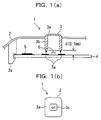
- Fig. 1a is a cross-sectional view illustratively showing a configuration of an essential part of the touch switch
- Fig. 1b is a top view illustratively showing the configuration thereof.
- the touch switch 1 shown in Fig. 1a is provided in the interior of an automobile and is a switch mainly made in an instrument panel for audio equipment or air conditioner.
- a substrate 2 of the touch switch 1 is made of a milk-white ABS resin to have a sheet-like shape.
- the touch switch 1 can be formed into a complicated curved-surface shape according to a shape of an instrument panel. Moreover, the front surface side (upper surface side in the illustration) of this substrate 2 is formed as a designed surface exposed to the interior of the automobile while a plurality of reinforcing ribs (not shown) are made on the rear side non-designed surface of the substrate 2.
- the ABS resin is used as the substrate 2, it is also acceptable to use a different resin such as polypropylene, polycarbonate or acrylic.
- the present invention is not limited to the milk-white.
- the substrate 2 is made of a resin, for the formation of the substrate 2, any material having a non-conductive characteristic is also acceptable, and the material of the substrate 2 is not limited to a resin.
- a conductive member 3 for the touch detection is formed integrally with the substrate 2 by means of the insert molding or two-material molding.
- the conductive member 3 functions as a main unit of the switch and, when an operator touches this conductive member (which will be referred to hereinafter as a switch main unit) 3, an operation state of a device connected to the touch switch changes over.
- the switch main unit 3 is made of a resin material having a conductive characteristic and, concretely, it is made of a so-called conductive polymer having a chemical constitution enabling the electronic transition, a conductive resin composition made by incorporating a chemical compound or metallic grinding, such as interfacial action agent or electrolyte, or conductive filler including carbon, or other materials.
- the switch main unit 3 is composed of a top surface section (touch surface) 3a with which an operator comes directly into contact as illustrated and a wall section 3b extending from this top surface section 3a toward the back side. Still furthermore, the top surface section 3a of the switch main unit 3 is formed to be exposed on the front side of the substrate 2 (automobile interior side) and, as shown in Fig. 1b , a character(s) 3c, symbol mark(s) or the like indicating a touch switch function is drawn on a top surface of the switch main unit 3 through the use of a treatment such as the laser etching or two-material molding using a milk-white material.
- a treatment such as the laser etching or two-material molding using a milk-white material.
- an LED (light-emitting device) 6 for illumination is provided at a position confronting the top surface section 3a between the circuit board 4 and the top surface section 3a, and the top surface section 3a is made to allow the transmission of light from the LED 6 at the light emission of the LED 6.
- the thickness of the top surface section 3a is set so as to permit the transmission of light from the LED 6, thereby ensuring the permeability.
- the wall section 3b is formed along the shape of an edge portion of the top surface section 3a and, in this embodiment, it is made as a square column or pole formed to extend toward the backside of the panel 1.
- the circuit board 4 is provided at the backside of the substrate 2, and an electrostatic capacity detection circuit (pattern) 5 having a touch operation detection electrode 5a is printed onto this circuit board 4. Moreover, this circuit board 4 is engaged with and set in a claw portion(s) 2a extending from the substrate 2 toward the back side of the panel as illustrated. Incidentally, although in the illustration the claw portion 2a is set at only a single point, such a claw portion 2a is provided at a plurality of points so that the circuit board 4 can be fixedly secured to the substrate 2.
- the detection electrode 5a formed on the circuit board 4, is disposed at a position confronting a rear side end surface of the wall section 3b of the switch main unit 3 to be spaced by d from the rear-side-end surface thereof.
- the space d is set at a given dimension, so that, when an operator comes into contact with the switch main unit 3, a variation of the impedance is detectable.
- Patent Document 3 Japanese Patent Laid-Open No. 2007-35334
- Patent Document 3 Japanese Patent Laid-Open No. 2007-35334
- the output of a circuit 5 is enhanced in order to increase the sensitivity, an erroneous detection can occur because of the pickup of noise.
- the substrate 2, having a non-conductive characteristic, and the switch main unit 3, having a conductive characteristic are integrated with each other by means of the two-material molding to the substrate 2 so that the top surface section 3a of the switch main unit 3 shows up above a surface of the substrate 2, it is possible to realize a touch switch excellent in design while achieving a reliable touch detection.
- a gap is made between the detection electrode 5a and the wall section 3b of the switch main unit 3, which improves the assembling workability and facilitates the management of the dimension tolerance.
- the formation of a gap of approximately 0.1 mm eliminates the need for the strict management of the dimension tolerance, which enables the cost reduction.
- the LED 6 is mounted on this circuit board 4. This LED 6 works with an illumination switch of an automobile and lights up in a state linked to the lighting of the headlight. This improves the visibility of the touch switch 1 at night.
- the wall section 3b of the switch main unit 3 is made to have a shape surrounding the LED 6. That is, as mentioned above, the wall section 3b has a shape of a square column, and the positional relationship between the LED 6 and the switch main unit 3 is set so that the LED 6 is positioned inside of this square column. In this case, the wall section 3b has a thickness set so as to shield the irradiated light from the LED 6; thus, functions as a shielding wall. That is, the leakage of light from the LED 6 makes the illumination blurry at night, which may lower the visibility or hurt the outward appearance.
- the thickness of the wall section 3b is set at a given value so as to inhibit the light from passing through it.
- the irradiated light from the LED 6 is applied toward only the top surface section 3a, which can reliably light the switch top surface section 3a even at night.
- the structured touch switch according to the embodiment of the present invention can provide the following effects and advantages.
- this touch switch 1 since the switch main unit 3 is formed with a conductive member and a portion thereof is made to appear at the substrate 2 so that the top surface section 3a functions as a touch surface, the touch detection can be made with high accuracy. This can eliminate the need for the enhancement of the electrical output of the electrostatic capacity detection circuit 5, which enables the suppression of the occurrence of noise, thereby allowing this touch switch 1 to be employed for a control panel (particularly, an instrument panel of an automobile) on which a plurality of (or a large number of) switches are in an adjoining condition.
- the wall section 3b can easily acquire a light interception characteristic when it is formed to have an appropriate thickness.
- the irradiated light from the LED 6 penetrates the top surface section 3a at lighting so as to enable a character (or a symbol mark) made on the top surface section 3a to come up and appear, which improves the visibility at night.
- a space d defined between the detection electrode 5a of the electrostatic capacity detection circuit 5 and the wall section 3b of the switch main unit 3, facilitates the dimension management and achieves the cost reduction. Still moreover, the formation of the space d allows the employment of a simple assembling technique in which the circuit board 4 and the panel 2 are attached to each other by means of the engagement with the claw portions 2a of the panel 2, which contributes to further cost reduction.
- the substrate 2 is made of a non-conductive resin and the switch main unit 3 is made of a conductive resin
- these two members can be formed integrally with each other through the use of the insert molding or two-material molding which has been well known so far, which achieves further cost reduction.
- the attachment of the circuit board 4 to the substrate 2 is not limited to the engagement with the claw portions, and it is also appropriate that, for example, a boss portion is made vertically on the rear surface side of the substrate 2 and the circuit board may be attached to this boss portion with a screw (vis).
- the light-emitting device is not limited to the LED, and various types of light-emitting devices are also employable.
Landscapes
- Switches That Are Operated By Magnetic Or Electric Fields (AREA)
Applications Claiming Priority (1)
| Application Number | Priority Date | Filing Date | Title |
|---|---|---|---|
| JP2007154445A JP4843564B2 (ja) | 2007-06-11 | 2007-06-11 | タッチスイッチの構造 |
Publications (3)
| Publication Number | Publication Date |
|---|---|
| EP2003778A2 true EP2003778A2 (de) | 2008-12-17 |
| EP2003778A3 EP2003778A3 (de) | 2011-05-25 |
| EP2003778B1 EP2003778B1 (de) | 2013-11-06 |
Family
ID=39773033
Family Applications (1)
| Application Number | Title | Priority Date | Filing Date |
|---|---|---|---|
| EP08010057.1A Ceased EP2003778B1 (de) | 2007-06-11 | 2008-06-02 | Berührungsschalter |
Country Status (6)
| Country | Link |
|---|---|
| US (1) | US8110767B2 (de) |
| EP (1) | EP2003778B1 (de) |
| JP (1) | JP4843564B2 (de) |
| KR (1) | KR100990619B1 (de) |
| CN (1) | CN101325412B (de) |
| RU (1) | RU2383959C1 (de) |
Cited By (2)
| Publication number | Priority date | Publication date | Assignee | Title |
|---|---|---|---|---|
| FR2982968A1 (fr) * | 2011-11-21 | 2013-05-24 | Atlantic Industrie Sas | Facade tactile de systeme electronique dont les parametres de fonctionnement sont modifies par l'intervention physique de l'utilisateur |
| EP2919387A1 (de) * | 2014-03-07 | 2015-09-16 | Alps Electric Co., Ltd. | Elektrostatische kapazitätseingabevorrichtung |
Families Citing this family (20)
| Publication number | Priority date | Publication date | Assignee | Title |
|---|---|---|---|---|
| US8115494B2 (en) * | 2009-04-03 | 2012-02-14 | General Electric Company | Systems, methods, and apparatus for rub detection in a machine |
| US8859922B1 (en) * | 2009-10-18 | 2014-10-14 | Method Electronics, Inc. | Multi-function switch apparatus and method of use |
| US8552746B2 (en) * | 2010-12-22 | 2013-10-08 | Visteon Global Technologies, Inc. | Proximity sensor including a multilayer elastomer assembly |
| DE102011006021A1 (de) * | 2011-03-24 | 2012-09-27 | E.G.O. Elektro-Gerätebau GmbH | Bedieneinrichtung für ein Elektrogerät |
| JP2013077555A (ja) * | 2011-09-12 | 2013-04-25 | Futaba Corp | タッチスイッチ |
| JP5127980B1 (ja) | 2011-12-26 | 2013-01-23 | 株式会社東芝 | 電子機器 |
| JP5498557B2 (ja) * | 2012-10-25 | 2014-05-21 | 株式会社東芝 | 電子機器 |
| CN105074863B (zh) | 2013-04-01 | 2017-03-08 | 株式会社电装 | 静电电容式开关 |
| CN104168009B (zh) * | 2013-05-17 | 2018-03-23 | 光宝电子(广州)有限公司 | 发光型触控开关装置及发光型触控开关模组 |
| RU2559695C2 (ru) * | 2013-05-29 | 2015-08-10 | Шепеленко Виталий Борисович | Электронный индикатор |
| RU2559697C2 (ru) * | 2013-05-29 | 2015-08-10 | Шепеленко Виталий Борисович | Устройство индикации вмешательства |
| RU2559696C2 (ru) * | 2013-05-29 | 2015-08-10 | Шепеленко Виталий Борисович | Электронный индикатор и способ его применения |
| RU2559700C2 (ru) * | 2013-05-29 | 2015-08-10 | Шепеленко Виталий Борисович | Способ контроля доступа к объекту и устройство для его реализации |
| RU2559699C2 (ru) * | 2013-05-29 | 2015-08-10 | Шепеленко Виталий Борисович | Крепежное средство для выявления несанкционированного вмешательства |
| RU2559694C2 (ru) * | 2013-05-29 | 2015-08-10 | Шепеленко Виталий Борисович | Электронное пломбировочное устройство |
| JP5904598B2 (ja) * | 2013-10-31 | 2016-04-13 | アルプス電気株式会社 | 操作装置及び該操作装置を用いた車両用操作装置 |
| KR101804636B1 (ko) * | 2015-10-30 | 2017-12-05 | 엘에스오토모티브 주식회사 | 터치 스위치 유니트 및 이를 구비하는 차량 실내 조명 장치 |
| KR101795540B1 (ko) * | 2016-07-04 | 2017-11-10 | 현대자동차주식회사 | 터치 입력장치 |
| WO2019058556A1 (ja) * | 2017-09-25 | 2019-03-28 | 三菱電機株式会社 | 空気調和機 |
| KR102236099B1 (ko) * | 2019-10-25 | 2021-04-05 | 삼성전기주식회사 | 멀티 터치의 위치 식별이 가능한 터치 센싱 장치 및 전자 기기 |
Citations (6)
| Publication number | Priority date | Publication date | Assignee | Title |
|---|---|---|---|---|
| US4045629A (en) | 1974-04-12 | 1977-08-30 | Bassani Ticione S.P.A. | Electrical proximity switch arrangements |
| US4394643A (en) | 1981-04-29 | 1983-07-19 | Whirlpool Corporation | Capacitive touch panel control |
| JP2004022356A (ja) | 2002-06-17 | 2004-01-22 | Omron Corp | タッチスイッチ |
| JP2006196395A (ja) | 2005-01-17 | 2006-07-27 | Kojima Press Co Ltd | タッチスイッチ |
| JP2007035334A (ja) | 2005-07-25 | 2007-02-08 | Calsonic Kansei Corp | 静電容量式タッチスイッチ |
| US20070095643A1 (en) | 2004-04-15 | 2007-05-03 | E.G.O. Elektro-Geraetebau Gmbh | Operating device with a touch switch |
Family Cites Families (18)
| Publication number | Priority date | Publication date | Assignee | Title |
|---|---|---|---|---|
| CA1152603A (en) * | 1979-09-28 | 1983-08-23 | Bfg Glassgroup | Capacitive systems for touch control switching |
| JPH03225719A (ja) * | 1990-01-29 | 1991-10-04 | Matsushita Electric Works Ltd | 非接触スイッチ |
| JPH0773790A (ja) * | 1993-07-07 | 1995-03-17 | Komatsu Raito Seisakusho:Kk | 自動販売機の商品等選択スイッチ装置 |
| JPH0997525A (ja) * | 1995-09-28 | 1997-04-08 | Harman Co Ltd | スイッチ |
| JPH1050172A (ja) * | 1996-05-01 | 1998-02-20 | Kubota Corp | 自動販売機の押しボタンスイッチ装置 |
| ATE216541T1 (de) * | 1997-02-17 | 2002-05-15 | Ego Elektro Geraetebau Gmbh | Berührungsschalter mit sensortaste |
| DE19714195A1 (de) * | 1997-04-07 | 1998-10-08 | Aeg Hausgeraete Gmbh | Verfahren und Vorrichtung zum Einstellen eines Betriebszustandes eines Haushaltsgerätes an einem mit einer Anzeige versehenen Bedienelement |
| US6483054B2 (en) * | 2000-02-29 | 2002-11-19 | Yazaki Corporation | Pressure-sensitive sensor, connector and combining structure thereof |
| RU2267183C2 (ru) * | 2000-05-22 | 2005-12-27 | Диджит Уайрлесс, Ллс | Устройства ввода и их использование |
| DE10123633A1 (de) * | 2001-05-09 | 2003-02-06 | Ego Elektro Geraetebau Gmbh | Sensorelement |
| DE20119700U1 (de) * | 2001-11-29 | 2002-02-14 | E.G.O. Control Systems GmbH & Co. KG, 72336 Balingen | Sensorvorrichtung |
| JP4295468B2 (ja) * | 2001-12-21 | 2009-07-15 | ポリマテック株式会社 | 照光式押釦スイッチ用カバー部材 |
| KR100499807B1 (ko) | 2002-10-30 | 2005-07-08 | 에이디반도체(주) | 정전용량 스위치 |
| DE102004026315A1 (de) * | 2004-05-26 | 2005-12-29 | Electrolux Home Products Corporation N.V. | Vorrichtung und Verfahren zur Sicherung eines Haushaltsgeräts von unbeabsichtigtem Betrieb |
| JP4082402B2 (ja) | 2004-10-19 | 2008-04-30 | 松下電器産業株式会社 | タッチキーを用いた電磁調理器 |
| GB0505451D0 (en) * | 2005-03-17 | 2005-04-20 | Waddington George | Improvements in rotary controls |
| DE102006005581B4 (de) * | 2006-02-06 | 2007-10-04 | Diehl Ako Stiftung & Co. Kg | Kapazitiver Berührungsschalter |
| TWD120590S1 (zh) * | 2006-07-24 | 2007-12-21 | 本田技研工業股份有限公司 | 汽車用中控台 |
-
2007
- 2007-06-11 JP JP2007154445A patent/JP4843564B2/ja not_active Expired - Fee Related
-
2008
- 2008-04-01 KR KR1020080030102A patent/KR100990619B1/ko not_active Expired - Fee Related
- 2008-06-02 EP EP08010057.1A patent/EP2003778B1/de not_active Ceased
- 2008-06-06 US US12/155,627 patent/US8110767B2/en not_active Expired - Fee Related
- 2008-06-10 RU RU2008123720/09A patent/RU2383959C1/ru active
- 2008-06-10 CN CN2008101108111A patent/CN101325412B/zh not_active Expired - Fee Related
Patent Citations (6)
| Publication number | Priority date | Publication date | Assignee | Title |
|---|---|---|---|---|
| US4045629A (en) | 1974-04-12 | 1977-08-30 | Bassani Ticione S.P.A. | Electrical proximity switch arrangements |
| US4394643A (en) | 1981-04-29 | 1983-07-19 | Whirlpool Corporation | Capacitive touch panel control |
| JP2004022356A (ja) | 2002-06-17 | 2004-01-22 | Omron Corp | タッチスイッチ |
| US20070095643A1 (en) | 2004-04-15 | 2007-05-03 | E.G.O. Elektro-Geraetebau Gmbh | Operating device with a touch switch |
| JP2006196395A (ja) | 2005-01-17 | 2006-07-27 | Kojima Press Co Ltd | タッチスイッチ |
| JP2007035334A (ja) | 2005-07-25 | 2007-02-08 | Calsonic Kansei Corp | 静電容量式タッチスイッチ |
Cited By (3)
| Publication number | Priority date | Publication date | Assignee | Title |
|---|---|---|---|---|
| FR2982968A1 (fr) * | 2011-11-21 | 2013-05-24 | Atlantic Industrie Sas | Facade tactile de systeme electronique dont les parametres de fonctionnement sont modifies par l'intervention physique de l'utilisateur |
| EP2597774A1 (de) | 2011-11-21 | 2013-05-29 | Atlantic Industrie | Berührungsempfindliche Fassade eines elektronischen System, dessen Funktionsparameter durch das physische Eingreifen des Benutzers verändert werden |
| EP2919387A1 (de) * | 2014-03-07 | 2015-09-16 | Alps Electric Co., Ltd. | Elektrostatische kapazitätseingabevorrichtung |
Also Published As
| Publication number | Publication date |
|---|---|
| RU2008123720A (ru) | 2009-12-27 |
| JP2008305766A (ja) | 2008-12-18 |
| US8110767B2 (en) | 2012-02-07 |
| JP4843564B2 (ja) | 2011-12-21 |
| KR100990619B1 (ko) | 2010-10-29 |
| KR20080108899A (ko) | 2008-12-16 |
| RU2383959C1 (ru) | 2010-03-10 |
| CN101325412A (zh) | 2008-12-17 |
| CN101325412B (zh) | 2012-01-18 |
| EP2003778A3 (de) | 2011-05-25 |
| US20080302649A1 (en) | 2008-12-11 |
| EP2003778B1 (de) | 2013-11-06 |
Similar Documents
| Publication | Publication Date | Title |
|---|---|---|
| EP2003778B1 (de) | Berührungsschalter | |
| US8148659B2 (en) | Touch switch structure | |
| CN1885719B (zh) | 带有接近传感器的控制元件 | |
| CN114127876A (zh) | 具有可移动开关元件的致动装置、车辆以及致动方法 | |
| US7129432B2 (en) | Lighted switch unit | |
| CN1885718B (zh) | 具有接近传感器和屏蔽作用的控制元件 | |
| US11801752B2 (en) | Motor vehicle control device | |
| JP2002313181A (ja) | 操作パネル装置 | |
| JP2015181087A (ja) | 静電容量式入力装置 | |
| EP3667691B1 (de) | Eingabevorgangsvorrichtung | |
| CN113168982A (zh) | 装置以及操作装置 | |
| JP2014235893A (ja) | コントロールパネル | |
| JP2016205979A (ja) | 計器装置 | |
| JP2012150932A (ja) | 回転操作体及びこれを用いた回転操作型入力装置 | |
| JP6040925B2 (ja) | 静電容量式スイッチ | |
| CN105074863B (zh) | 静电电容式开关 | |
| JP4644611B2 (ja) | 車両のセンターパネル構造体 | |
| CN211695443U (zh) | 操作装置以及热水供给装置 | |
| JP6040841B2 (ja) | 静電容量式スイッチ | |
| JP6044423B2 (ja) | 静電容量式スイッチ | |
| WO2014162668A1 (ja) | 静電容量式スイッチ | |
| JPH09243147A (ja) | 空調用設定器 | |
| CN110690066A (zh) | 开关装置 |
Legal Events
| Date | Code | Title | Description |
|---|---|---|---|
| PUAI | Public reference made under article 153(3) epc to a published international application that has entered the european phase |
Free format text: ORIGINAL CODE: 0009012 |
|
| AK | Designated contracting states |
Kind code of ref document: A2 Designated state(s): AT BE BG CH CY CZ DE DK EE ES FI FR GB GR HR HU IE IS IT LI LT LU LV MC MT NL NO PL PT RO SE SI SK TR |
|
| AX | Request for extension of the european patent |
Extension state: AL BA MK RS |
|
| PUAL | Search report despatched |
Free format text: ORIGINAL CODE: 0009013 |
|
| AK | Designated contracting states |
Kind code of ref document: A3 Designated state(s): AT BE BG CH CY CZ DE DK EE ES FI FR GB GR HR HU IE IS IT LI LT LU LV MC MT NL NO PL PT RO SE SI SK TR |
|
| AX | Request for extension of the european patent |
Extension state: AL BA MK RS |
|
| 17P | Request for examination filed |
Effective date: 20111125 |
|
| AKX | Designation fees paid |
Designated state(s): DE FR GB |
|
| 17Q | First examination report despatched |
Effective date: 20120305 |
|
| RBV | Designated contracting states (corrected) |
Designated state(s): DE FR GB |
|
| GRAP | Despatch of communication of intention to grant a patent |
Free format text: ORIGINAL CODE: EPIDOSNIGR1 |
|
| INTG | Intention to grant announced |
Effective date: 20130424 |
|
| GRAS | Grant fee paid |
Free format text: ORIGINAL CODE: EPIDOSNIGR3 |
|
| GRAA | (expected) grant |
Free format text: ORIGINAL CODE: 0009210 |
|
| AK | Designated contracting states |
Kind code of ref document: B1 Designated state(s): DE FR GB |
|
| REG | Reference to a national code |
Ref country code: GB Ref legal event code: FG4D |
|
| REG | Reference to a national code |
Ref country code: DE Ref legal event code: R096 Ref document number: 602008028485 Country of ref document: DE Effective date: 20140102 |
|
| REG | Reference to a national code |
Ref country code: DE Ref legal event code: R097 Ref document number: 602008028485 Country of ref document: DE |
|
| PLBE | No opposition filed within time limit |
Free format text: ORIGINAL CODE: 0009261 |
|
| STAA | Information on the status of an ep patent application or granted ep patent |
Free format text: STATUS: NO OPPOSITION FILED WITHIN TIME LIMIT |
|
| 26N | No opposition filed |
Effective date: 20140807 |
|
| REG | Reference to a national code |
Ref country code: DE Ref legal event code: R097 Ref document number: 602008028485 Country of ref document: DE Effective date: 20140807 |
|
| REG | Reference to a national code |
Ref country code: FR Ref legal event code: PLFP Year of fee payment: 9 |
|
| REG | Reference to a national code |
Ref country code: FR Ref legal event code: PLFP Year of fee payment: 10 |
|
| REG | Reference to a national code |
Ref country code: FR Ref legal event code: PLFP Year of fee payment: 11 |
|
| PGFP | Annual fee paid to national office [announced via postgrant information from national office to epo] |
Ref country code: DE Payment date: 20200519 Year of fee payment: 13 Ref country code: FR Payment date: 20200512 Year of fee payment: 13 |
|
| PGFP | Annual fee paid to national office [announced via postgrant information from national office to epo] |
Ref country code: GB Payment date: 20200520 Year of fee payment: 13 |
|
| REG | Reference to a national code |
Ref country code: DE Ref legal event code: R119 Ref document number: 602008028485 Country of ref document: DE |
|
| GBPC | Gb: european patent ceased through non-payment of renewal fee |
Effective date: 20210602 |
|
| PG25 | Lapsed in a contracting state [announced via postgrant information from national office to epo] |
Ref country code: GB Free format text: LAPSE BECAUSE OF NON-PAYMENT OF DUE FEES Effective date: 20210602 Ref country code: DE Free format text: LAPSE BECAUSE OF NON-PAYMENT OF DUE FEES Effective date: 20220101 |
|
| PG25 | Lapsed in a contracting state [announced via postgrant information from national office to epo] |
Ref country code: FR Free format text: LAPSE BECAUSE OF NON-PAYMENT OF DUE FEES Effective date: 20210630 |