EP1998456A2 - Übertragungsvorrichtung - Google Patents
Übertragungsvorrichtung Download PDFInfo
- Publication number
- EP1998456A2 EP1998456A2 EP20080156951 EP08156951A EP1998456A2 EP 1998456 A2 EP1998456 A2 EP 1998456A2 EP 20080156951 EP20080156951 EP 20080156951 EP 08156951 A EP08156951 A EP 08156951A EP 1998456 A2 EP1998456 A2 EP 1998456A2
- Authority
- EP
- European Patent Office
- Prior art keywords
- switch
- power amp
- power amplifier
- transmission device
- distortion compensator
- Prior art date
- Legal status (The legal status is an assumption and is not a legal conclusion. Google has not performed a legal analysis and makes no representation as to the accuracy of the status listed.)
- Granted
Links
Images


Classifications
-
- H—ELECTRICITY
- H03—ELECTRONIC CIRCUITRY
- H03F—AMPLIFIERS
- H03F3/00—Amplifiers with only discharge tubes or only semiconductor devices as amplifying elements
- H03F3/72—Gated amplifiers, i.e. amplifiers which are rendered operative or inoperative by means of a control signal
Definitions
- the present invention relates to a transmission device, and in particular to a transmission device, provided with a radio frequency or high frequency (hereinafter, represented by RF) power amplifier, applied to a radio base station.
- RF radio frequency or high frequency
- An RF power amplifier (hereinafter, abbreviated as amp) in a transmission device applied to a radio base station has the following functions:
- a distortion compensator 1 when having received data X (I, Q) of a base band as an input, a distortion compensator 1 multiplies to the input data a distortion compensating coefficient of an RF power amp 6.
- An output signal of the distortion compensator 1 applied with the distortion compensating coefficient is converted by a D/A converter 2 into an analog IQ signal to be provided to a modulator 3.
- This modulator 3 performs a direct modulation with a local oscillator 4 of a carrier frequency (for example, 2.1 GHz bandwidth) to generate an RF signal.
- the RF signal thus generated passes through a coupler 5 that forms an input signal detector of an RF power amp 6 and inputted to the amp 6.
- a signal power-amplified by the RF power amp 6 passes through a coupler 7 that forms an output signal detector of the RF power amp 6 together with a coupler 13 and transmitted to an antenna 8.
- the couplers 5 and 7 respectively branch their input signals to an amp input monitor terminal 11a and an amp output monitor terminal 11b, and that a source of the RF power amp 6 is switched ON or OFF by a power amp switch 10.
- the coupler 13 For updating the distortion compensating coefficient of the distortion compensator 1, the coupler 13 provides a branched signal from its input signal to a frequency converter 15, which downconverts its input signal into an intermediate frequency (IF) signal with a local oscillator 16.
- the output signal of the frequency converter 15 is converted into a digital signal by an A/D converter 17 and provided to the distortion compensator 1, forming a feedback route.
- the distortion compensator 1 compares the input data X (I, Q) with the feedback data from the A/D converter 17 to update the distortion compensating coefficient, thereby suppressing distortion components of the RF power amp 6.
- a switching signal KS from the power amp switch 10 When a switching signal KS from the power amp switch 10 is made OFF or reset, the source within the RF power amp 6 is powered down so that its transmission output is suspended. For example, when experiments are desired to be performed while suspending the transmission output of the power amp 6, the power amp switch 10 is made OFF, whereby in the absence of a transmission wave from the antenna 8, such an event that the RF power amp 6 is faulted due to a reflecting wave does not occur even though the output of the antenna 8 is not terminated.
- the amp input monitor terminal 11a outputs the input signal of the RF power amp 6 which is branched at the coupler 5, which is used in such a case where the transmission wave is required to be confirmed at the above experiments. Even at the suppression of the RF power amp 6, a signal comes in up to the input terminal of the RF power amp 6, so that the transmission wave can be recognized by monitoring the signal.
- the amp output monitor terminal 11b provides the output signal of the RF power amp 6 coupled by e.g. several 10 dB at the coupler 7. This enables the transmission output waveform to be recognized at the output terminal of the RF power amp 6 even upon the antenna 8 being connected, and also the transmission output level to be recognized if a coupling quantity of the coupler 7 is prescribed. It is of course that the transmission waveform can not be observed when the power amp switch 10 is made OFF.
- the above arrangement is disadvantageous in that it has two monitor terminals, i.e. an amp input monitor terminal and an amp output monitor terminal, causing the surface area of the device to be enlarged.
- the above arrangement uses the amp input monitor terminal at the time when the source of the power amp is turned or switched OFF, while using the amp output monitor terminal at the time when the source of the power amp is switched ON. Therefore, each time the power amp is switched ON or OFF, the connections of the monitor terminals have to be changed, resulting in a poor operability.
- a predistortion type distortion compensation is a technology for decreasing distortions at the output terminal of the power amp by predicting a distortion quantity f(p) based on a non-linear characteristic of the power amp and applying a signal preliminarily multiplied with a reverse distortion characteristic h(p) of the power amp to the input signal x(p) (step S100) (step S200). Resultantly, at the amp input monitor terminal, a signal h(p) * x(p) applied with the reverse distortion characteristic h(p) of the power amp is to be observed.
- the amp input monitor terminal and the amp output monitor terminal are unified as a single terminal to selectively monitor the amp input waveform or the amp output waveform in association with the power amp switch being made ON or OFF.
- the output signal of the power amp is selected when the power amp switch is, for example, made ON, while the input signal of the power amp is selected when the power amp switch is made OFF, to be provided as an output from the monitor terminal.
- the transmission device may further comprise, in addition to the arrangement of the above [1], a distortion compensator provided in a front stage of the input signal detector, a feedback route connected to the distortion compensator, and a second RF switch selecting an input signal or output signal of the power amp to be transmitted to the distortion compensator through the feedback route, in association with the power amp switch being switched ON or OFF.
- each of the above detectors may be composed of two couplers one of which branches its input signal to each RF switch.
- the transmission device may further comprise, in addition to the arrangement of the above [1], a distortion compensator provided in a front stage of the power amp, a feedback route feeding back the output signal of the power amp to the distortion compensator, and a selector validating or invalidating the distortion compensator, in association with the power amp switch being switched ON or OFF.
- the transmission device may further comprise a series circuit including a distortion compensator, a D/A converter, and a modulator connected in a front stage of the input signal detector, wherein the input signal detector comprises a single coupler, the output signal detector comprises two couplers respectively branching the input signals to the RF switch and the feedback route, and the selector comprises a selector making the distortion compensator connect to the D/A converter or bypassed, in association with the power amp switch being switched ON or OFF.
- the above mentioned feedback route may comprise a frequency converter and an A/D converter connected between the couplers of the output signal detector and the distortion compensator.
- the present invention it is made possible to decrease the number of a monitor terminal of an RF power amp, and to monitor waveforms with less distortion components not only at the output but also the input of the power amp, depending on the power amp being made ON or OFF.
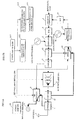
- Fig.1 shows an embodiment [1] of a transmission device, in which an RF switch 9 is added to the prior art transmission device shown in Fig.10 .
- the input signal of the coupler 5 and the input signal of the coupler 7 are respectively branched and provided to the RF switch 9; the switching signal KS from the power amp switch 10 is provided to the RF power amp 6 as well as the RF switch 9; the output signal of the RF switch 9 is provided to a single monitor terminal 11.
- a feedback route to the distortion compensator 1 is not connected.
- Figs.2 and 3 illustrate specific operations, in the arrangement of Fig.1 , where a monitoring signal for the RF power amp 6 is selected by the power amp switch 10.
- input data X (I, Q) from a base band portion are multiplied with a distortion compensating coefficient by the distortion compensator 1, converted into an analog signal by the D/A converter 2, modulated by the modulator 3, passed through the coupler 5, and is provided to the RF power amp 6 for monitoring the input wave thereof.
- the output signal of the RF power amp 6 passes through the coupler 7 and is transmitted from the antenna 8.
- the output signal (switching signal) KS of the power amp switch 10 indicates ON state (step S1 in Fig.2B ), making the source of the RF power amp 6 ON (step S2) and switching the RF switch 9 over to the connection of a thick line shown.
- the RF switch 9 selects the signal branched from the coupler 7 or the output signal of the power amp 6 within the signals branched from the couplers 5 and 7 (step S3), to be transmitted from the antenna 8.
- Fig.3A illustrates an operation at the time when the switching signal KS from the power amp switch 10 is made OFF.
- the source of the RF power amp 6 is made OFF (step S12) while at the same time the output of the RF switch 9 is switched over to the input side of the RF power amp 6 (step S13).
- no transmission signal is provided to the antenna 8, so that even though the antenna 8 is opened (even in the state of total reflection) the RF power amp 6 will not fail or excessive heat generation will not occur.
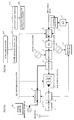
- Fig.4 shows an embodiment [2] of a transmission device, which is different from the above embodiment [1] in that there is provided a feedback route to the distortion compensator 1 to reduce distortion components of the output of the power amp 6.
- a signal branched from the coupler 13 is fedback to the distortion compensator 1 via the frequency converter 15 and the A/D converter 17, and besides there is provided another RF switch 14, between the coupler 13 and the frequency converter 15 under control of the switching signal KS concurrently with the power amp 6 and the RF switch 9.
- a signal branched from a coupler 12 connected between the modulator 3 and the coupler 5 is provided in addition to the signal branched from the coupler 13, and the output of the RF switch 14 is provided to the frequency converter 15.
- Figs.5 and 6 illustrate specific operations, where the monitoring output of the RF power amp 6 is variously switched over in association with the power amp switch 10.
- the input data X (I, Q) is multiplied with a distortion compensating coefficient by the distortion compensator 1, converted into an analog signal by the D/A converter 2, and then modulated by the modulator 3, forming an input signal of the RF power amp 6.
- This input signal is obtained after having passed through the coupler 12 for feedback and the coupler 5 for monitor, both of which form an input signal detector.
- An output wave amplified by the RF power amp 6 passes through the coupler 13 for feedback and the coupler 7 for monitor, both of which form an output signal detector, and is transmitted from the antenna 8.
- step S31 in Fig.5B When the switching signal KS from the power amp switch 10 is made ON (step S31 in Fig.5B ), the source of the RF power amp 6 is powered on (step S32), at which time the RF switch 14 which forms a feedback route switching portion is switched over to the amp output side (step S33) to perform distortion compensating operations. Namely, since the feedback route is connected from the output side of the RF power amp 6, an output waveform with less distortion can be obtained from the antenna 8 (step S34).
- Fig.6A shows a state where the switching signal KS from the power amp switch 10 is made OFF (step S41 in Fig.6B ).
- the switching signal KS is made OFF
- the source of the RF power amp 6 is made OFF (step S42)
- the RF switch 14 as a feedback route switching portion selects the branched signal of the coupler 12 on the input side of the RF power amp 6 (step S43) to perform distortion compensating operations.
- the feedback route is connected on the input side of the RF power amp 6, waveforms in which distortion components which can exist on the input side of the power amp 6 are compensated by the distortion compensator 1 can be obtained from the monitor terminal 11.
- Fig.7 shows an embodiment [3] of a transmission device.
- This embodiment [3] is different from the above embodiment [1] in that for outputting a modulated wave as it is with the distortion compensating function being suspended, the same feedback route as the prior art shown in Fig. 10 is provided, and a selector 18 is provided for validating/invalidating the distortion compensator 1 controlled by the feedback route in association with the switching signal KS from the power amp switch 10 being made ON or OFF. Therefore, this embodiment [3] only has to use a single coupler as an input signal detector.
- Figs.8 and 9 illustrate specific operations where the monitoring output of the RF power amp 6 is variously switched over in association with the power amp switch 10.
- the RF power amp 6 is made ON (step S62), and the selector 18 selects the distortion compensator 1 as shown by a thick line (step S63) to perform the distortion compensation with the input data X (I, Q) multiplied with a distortion compensating coefficient (step S64).
- the feedback route is connected from the output side of the RF power amp 6, so that an output waveform with less distortion can be obtained from the antenna 8.
- the RF switch 9 transmits the branched signal from the coupler 7, that is an output signal of the RF power amp 6 to the monitor terminal 11 as with the above Figs.2 and 5 .
- Fig.9A shows a state where the switching signal KS from the power amp switch 10 is made OFF.
- the power amp switch 10 is powered down (step S71 in Fig.9B )
- the source of the RF power amp 6 is made OFF (step S72) and concurrently the RF switch 9 selects the branched signal of the coupler 5, that is an input signal of the RF power amp 6, to be provided to the monitor terminal 11.
- a through input at the selector 18 is made active (step S73), so that the distortion compensator 1 is bypassed to invalidate the distortion compensating operation (step S74).
- a route without the multiplication of the distortion compensating coefficient by the distortion compensator 1 is selected or no distortion compensation is applied, where distortion components arising on the input side of the RF power amp 6 are inherently little, so that distortions become less than the waveform in the application of the distortion compensating coefficient for the power amp 6, enabling waveforms with less distortions (wave only applied with modulation) to be monitored at the monitor terminal 11.
Landscapes
- Engineering & Computer Science (AREA)
- Power Engineering (AREA)
- Transmitters (AREA)
- Amplifiers (AREA)
Applications Claiming Priority (1)
| Application Number | Priority Date | Filing Date | Title |
|---|---|---|---|
| JP2007147205A JP4757231B2 (ja) | 2007-06-01 | 2007-06-01 | 送信装置 |
Publications (3)
| Publication Number | Publication Date |
|---|---|
| EP1998456A2 true EP1998456A2 (de) | 2008-12-03 |
| EP1998456A3 EP1998456A3 (de) | 2014-12-03 |
| EP1998456B1 EP1998456B1 (de) | 2015-09-02 |
Family
ID=39714132
Family Applications (1)
| Application Number | Title | Priority Date | Filing Date |
|---|---|---|---|
| EP08156951.9A Ceased EP1998456B1 (de) | 2007-06-01 | 2008-05-27 | Übertragungsvorrichtung |
Country Status (4)
| Country | Link |
|---|---|
| US (1) | US7962107B2 (de) |
| EP (1) | EP1998456B1 (de) |
| JP (1) | JP4757231B2 (de) |
| CN (1) | CN101316107B (de) |
Families Citing this family (3)
| Publication number | Priority date | Publication date | Assignee | Title |
|---|---|---|---|---|
| JP6707883B2 (ja) * | 2016-02-05 | 2020-06-10 | 沖電気工業株式会社 | 送信機および歪補償方法 |
| CN111404014A (zh) * | 2020-01-15 | 2020-07-10 | 佛山市宝光新宇实业有限公司 | 脉冲激光器及其监控系统 |
| CN114448884B (zh) * | 2022-03-02 | 2023-10-20 | 深圳市友华通信技术有限公司 | 一种路由设备、路由设备的功率校准方法及存储介质 |
Citations (1)
| Publication number | Priority date | Publication date | Assignee | Title |
|---|---|---|---|---|
| JPH09312578A (ja) | 1996-05-22 | 1997-12-02 | Matsushita Electric Ind Co Ltd | 複数モード共用送信回路 |
Family Cites Families (14)
| Publication number | Priority date | Publication date | Assignee | Title |
|---|---|---|---|---|
| JPH0413444Y2 (de) * | 1989-07-05 | 1992-03-30 | ||
| JP3611690B2 (ja) * | 1996-10-14 | 2005-01-19 | 沖電気工業株式会社 | 半導体装置 |
| US6525605B2 (en) * | 1998-08-19 | 2003-02-25 | Harris Corporation | Power amplifier system having frequency and amplifier failure compensation |
| JP3274670B2 (ja) * | 1999-11-19 | 2002-04-15 | エヌイーシーケーブルメディア株式会社 | 双方向信号モニタ回路 |
| JP2002009556A (ja) * | 2000-06-16 | 2002-01-11 | Sony Corp | 歪補償装置及び歪補償方法 |
| JP2002314345A (ja) * | 2001-04-16 | 2002-10-25 | Sony Corp | 高周波増幅回路およびこれを用いた無線通信装置 |
| JP2005159672A (ja) * | 2003-11-25 | 2005-06-16 | Yagi Antenna Co Ltd | 広帯域増幅装置 |
| US7151405B2 (en) * | 2004-07-14 | 2006-12-19 | Raytheon Company | Estimating power amplifier non-linearity in accordance with memory depth |
| US7602155B2 (en) * | 2005-07-27 | 2009-10-13 | Artesyn Technologies, Inc. | Power supply providing ultrafast modulation of output voltage |
| US7761065B2 (en) * | 2006-02-03 | 2010-07-20 | Quantance, Inc. | RF power amplifier controller circuit with compensation for output impedance mismatch |
| US7509102B2 (en) * | 2006-04-07 | 2009-03-24 | Broadcom Corporation | DAC based switching power amplifier |
| US7558542B2 (en) * | 2006-06-09 | 2009-07-07 | Mediatek Inc. | System and method for providing a transmitter for polar modulation and power amplifier linearization |
| US7881401B2 (en) * | 2006-11-17 | 2011-02-01 | Infineon Technologies Ag | Transmitter arrangement and signal processing method |
| US7787564B1 (en) * | 2007-03-13 | 2010-08-31 | Kiomars Anvari | Combined peak reduction equalizer and phase/amplitude pre-distortion |
-
2007
- 2007-06-01 JP JP2007147205A patent/JP4757231B2/ja not_active Expired - Fee Related
-
2008
- 2008-05-27 EP EP08156951.9A patent/EP1998456B1/de not_active Ceased
- 2008-05-30 US US12/130,639 patent/US7962107B2/en active Active
- 2008-05-30 CN CN2008101081706A patent/CN101316107B/zh not_active Expired - Fee Related
Patent Citations (1)
| Publication number | Priority date | Publication date | Assignee | Title |
|---|---|---|---|---|
| JPH09312578A (ja) | 1996-05-22 | 1997-12-02 | Matsushita Electric Ind Co Ltd | 複数モード共用送信回路 |
Also Published As
| Publication number | Publication date |
|---|---|
| EP1998456B1 (de) | 2015-09-02 |
| CN101316107B (zh) | 2012-08-22 |
| JP2008301365A (ja) | 2008-12-11 |
| US20080299920A1 (en) | 2008-12-04 |
| CN101316107A (zh) | 2008-12-03 |
| US7962107B2 (en) | 2011-06-14 |
| JP4757231B2 (ja) | 2011-08-24 |
| EP1998456A3 (de) | 2014-12-03 |
Similar Documents
| Publication | Publication Date | Title |
|---|---|---|
| KR100844398B1 (ko) | 다중 레벨 전력 증폭기 | |
| US7489910B2 (en) | Wireless transmitter and amplifier | |
| US20160164466A1 (en) | Asymmetric Multilevel Backoff Amplifier with Radio-Frequency Splitter | |
| US20040183593A1 (en) | Power amplification apparatus of portable terminal | |
| US9837966B1 (en) | Series-type Doherty amplifier | |
| WO2013015778A1 (en) | Actively tuned circuit having parallel carrier and peaking paths | |
| EP0844732B1 (de) | Linearisierungsbrückenschaltung | |
| JPH09232992A (ja) | トランシーバのrfデュプレクサバイパス方法 | |
| EP1998456B1 (de) | Übertragungsvorrichtung | |
| WO2006082894A1 (ja) | 送信装置及び無線通信装置 | |
| US7254377B2 (en) | Parallel operation system of transmission amplifier | |
| US7420424B2 (en) | Power amplifier transmission line transformer | |
| CN112789508B (zh) | 使用低频相位和幅度调谐的毫米波有源负载牵引 | |
| US6326841B1 (en) | Method and apparatus for compensating for loss or RF output power from the isolation port of a hybrid coupler | |
| JP2010028799A (ja) | 受信システム | |
| JP2008022513A (ja) | 歪制御機能付き増幅装置 | |
| KR100371531B1 (ko) | 에러 피드백을 이용한 피드포워드 선형 전력 증폭기 | |
| KR101131910B1 (ko) | 이동통신시스템의 출력단 | |
| EP0784379B1 (de) | Nichtlineare Kompensationsschaltung | |
| KR20010027655A (ko) | 지연보상을 위한 증폭기를 가지는 피드포워드 방식의 선형 전력증폭기 | |
| WO2003065598A1 (en) | Power amplification apparatus of portable terminal | |
| JP2001196870A (ja) | 電力増幅器 | |
| EP1124334A1 (de) | Funkstation zum Senden und Empfang von Funksignalen | |
| EP1249086B1 (de) | Vorverzerrer mit nicht-magnetischen komponenten für eine nicht-lineare vorrichtung | |
| Singh et al. | PA Output Power and Efficiency Enhancement Across the 2: 1 VSWR Circle using Static Active Load Adjustment |
Legal Events
| Date | Code | Title | Description |
|---|---|---|---|
| PUAI | Public reference made under article 153(3) epc to a published international application that has entered the european phase |
Free format text: ORIGINAL CODE: 0009012 |
|
| AK | Designated contracting states |
Kind code of ref document: A2 Designated state(s): AT BE BG CH CY CZ DE DK EE ES FI FR GB GR HR HU IE IS IT LI LT LU LV MC MT NL NO PL PT RO SE SI SK TR |
|
| AX | Request for extension of the european patent |
Extension state: AL BA MK RS |
|
| PUAL | Search report despatched |
Free format text: ORIGINAL CODE: 0009013 |
|
| AK | Designated contracting states |
Kind code of ref document: A3 Designated state(s): AT BE BG CH CY CZ DE DK EE ES FI FR GB GR HR HU IE IS IT LI LT LU LV MC MT NL NO PL PT RO SE SI SK TR |
|
| AX | Request for extension of the european patent |
Extension state: AL BA MK RS |
|
| RIC1 | Information provided on ipc code assigned before grant |
Ipc: H03F 1/32 20060101ALI20141030BHEP Ipc: H03F 3/72 20060101ALI20141030BHEP Ipc: H04B 1/04 20060101AFI20141030BHEP |
|
| 17P | Request for examination filed |
Effective date: 20141217 |
|
| RBV | Designated contracting states (corrected) |
Designated state(s): AT BE BG CH CY CZ DE DK EE ES FI FR GB GR HR HU IE IS IT LI LT LU LV MC MT NL NO PL PT RO SE SI SK TR |
|
| GRAP | Despatch of communication of intention to grant a patent |
Free format text: ORIGINAL CODE: EPIDOSNIGR1 |
|
| INTG | Intention to grant announced |
Effective date: 20150325 |
|
| RAP1 | Party data changed (applicant data changed or rights of an application transferred) |
Owner name: FUJITSU LIMITED |
|
| RIN1 | Information on inventor provided before grant (corrected) |
Inventor name: NOHIRA, TOMOYOSHI Inventor name: SHAKO, HIDEHARU Inventor name: OHBA, TAKESHI |
|
| GRAS | Grant fee paid |
Free format text: ORIGINAL CODE: EPIDOSNIGR3 |
|
| GRAA | (expected) grant |
Free format text: ORIGINAL CODE: 0009210 |
|
| AKX | Designation fees paid |
Designated state(s): DE FR GB |
|
| AK | Designated contracting states |
Kind code of ref document: B1 Designated state(s): DE FR GB |
|
| REG | Reference to a national code |
Ref country code: GB Ref legal event code: FG4D |
|
| REG | Reference to a national code |
Ref country code: DE Ref legal event code: R096 Ref document number: 602008039900 Country of ref document: DE |
|
| REG | Reference to a national code |
Ref country code: FR Ref legal event code: PLFP Year of fee payment: 9 |
|
| REG | Reference to a national code |
Ref country code: DE Ref legal event code: R097 Ref document number: 602008039900 Country of ref document: DE |
|
| PLBE | No opposition filed within time limit |
Free format text: ORIGINAL CODE: 0009261 |
|
| STAA | Information on the status of an ep patent application or granted ep patent |
Free format text: STATUS: NO OPPOSITION FILED WITHIN TIME LIMIT |
|
| 26N | No opposition filed |
Effective date: 20160603 |
|
| REG | Reference to a national code |
Ref country code: FR Ref legal event code: PLFP Year of fee payment: 10 |
|
| REG | Reference to a national code |
Ref country code: FR Ref legal event code: PLFP Year of fee payment: 11 |
|
| PGFP | Annual fee paid to national office [announced via postgrant information from national office to epo] |
Ref country code: GB Payment date: 20180329 Year of fee payment: 11 |
|
| PGFP | Annual fee paid to national office [announced via postgrant information from national office to epo] |
Ref country code: DE Payment date: 20180515 Year of fee payment: 11 |
|
| PGFP | Annual fee paid to national office [announced via postgrant information from national office to epo] |
Ref country code: FR Payment date: 20180412 Year of fee payment: 11 |
|
| REG | Reference to a national code |
Ref country code: DE Ref legal event code: R119 Ref document number: 602008039900 Country of ref document: DE |
|
| GBPC | Gb: european patent ceased through non-payment of renewal fee |
Effective date: 20190527 |
|
| PG25 | Lapsed in a contracting state [announced via postgrant information from national office to epo] |
Ref country code: DE Free format text: LAPSE BECAUSE OF NON-PAYMENT OF DUE FEES Effective date: 20191203 Ref country code: GB Free format text: LAPSE BECAUSE OF NON-PAYMENT OF DUE FEES Effective date: 20190527 |
|
| PG25 | Lapsed in a contracting state [announced via postgrant information from national office to epo] |
Ref country code: FR Free format text: LAPSE BECAUSE OF NON-PAYMENT OF DUE FEES Effective date: 20190531 |