EP1995775A2 - Semiconductor device with stress reducing element - Google Patents
Semiconductor device with stress reducing element Download PDFInfo
- Publication number
- EP1995775A2 EP1995775A2 EP08156826A EP08156826A EP1995775A2 EP 1995775 A2 EP1995775 A2 EP 1995775A2 EP 08156826 A EP08156826 A EP 08156826A EP 08156826 A EP08156826 A EP 08156826A EP 1995775 A2 EP1995775 A2 EP 1995775A2
- Authority
- EP
- European Patent Office
- Prior art keywords
- reducing member
- stress reducing
- metal plate
- semiconductor device
- corner
- Prior art date
- Legal status (The legal status is an assumption and is not a legal conclusion. Google has not performed a legal analysis and makes no representation as to the accuracy of the status listed.)
- Granted
Links
Images



Classifications
-
- H—ELECTRICITY
- H10—SEMICONDUCTOR DEVICES; ELECTRIC SOLID-STATE DEVICES NOT OTHERWISE PROVIDED FOR
- H10W—GENERIC PACKAGES, INTERCONNECTIONS, CONNECTORS OR OTHER CONSTRUCTIONAL DETAILS OF DEVICES COVERED BY CLASS H10
- H10W40/00—Arrangements for thermal protection or thermal control
- H10W40/10—Arrangements for heating
-
- H—ELECTRICITY
- H10—SEMICONDUCTOR DEVICES; ELECTRIC SOLID-STATE DEVICES NOT OTHERWISE PROVIDED FOR
- H10W—GENERIC PACKAGES, INTERCONNECTIONS, CONNECTORS OR OTHER CONSTRUCTIONAL DETAILS OF DEVICES COVERED BY CLASS H10
- H10W40/00—Arrangements for thermal protection or thermal control
- H10W40/40—Arrangements for thermal protection or thermal control involving heat exchange by flowing fluids
- H10W40/47—Arrangements for thermal protection or thermal control involving heat exchange by flowing fluids by flowing liquids, e.g. forced water cooling
-
- H—ELECTRICITY
- H05—ELECTRIC TECHNIQUES NOT OTHERWISE PROVIDED FOR
- H05K—PRINTED CIRCUITS; CASINGS OR CONSTRUCTIONAL DETAILS OF ELECTRIC APPARATUS; MANUFACTURE OF ASSEMBLAGES OF ELECTRICAL COMPONENTS
- H05K3/00—Apparatus or processes for manufacturing printed circuits
- H05K3/0058—Laminating printed circuit boards onto other substrates, e.g. metallic substrates
- H05K3/0061—Laminating printed circuit boards onto other substrates, e.g. metallic substrates onto a metallic substrate, e.g. a heat sink
-
- H—ELECTRICITY
- H10—SEMICONDUCTOR DEVICES; ELECTRIC SOLID-STATE DEVICES NOT OTHERWISE PROVIDED FOR
- H10W—GENERIC PACKAGES, INTERCONNECTIONS, CONNECTORS OR OTHER CONSTRUCTIONAL DETAILS OF DEVICES COVERED BY CLASS H10
- H10W40/00—Arrangements for thermal protection or thermal control
- H10W40/20—Arrangements for cooling
- H10W40/25—Arrangements for cooling characterised by their materials
- H10W40/255—Arrangements for cooling characterised by their materials having a laminate or multilayered structure, e.g. direct bond copper [DBC] ceramic substrates
-
- H—ELECTRICITY
- H10—SEMICONDUCTOR DEVICES; ELECTRIC SOLID-STATE DEVICES NOT OTHERWISE PROVIDED FOR
- H10W—GENERIC PACKAGES, INTERCONNECTIONS, CONNECTORS OR OTHER CONSTRUCTIONAL DETAILS OF DEVICES COVERED BY CLASS H10
- H10W70/00—Package substrates; Interposers; Redistribution layers [RDL]
- H10W70/60—Insulating or insulated package substrates; Interposers; Redistribution layers
- H10W70/611—Insulating or insulated package substrates; Interposers; Redistribution layers for connecting multiple chips together
-
- H—ELECTRICITY
- H10—SEMICONDUCTOR DEVICES; ELECTRIC SOLID-STATE DEVICES NOT OTHERWISE PROVIDED FOR
- H10W—GENERIC PACKAGES, INTERCONNECTIONS, CONNECTORS OR OTHER CONSTRUCTIONAL DETAILS OF DEVICES COVERED BY CLASS H10
- H10W70/00—Package substrates; Interposers; Redistribution layers [RDL]
- H10W70/60—Insulating or insulated package substrates; Interposers; Redistribution layers
- H10W70/62—Insulating or insulated package substrates; Interposers; Redistribution layers characterised by their interconnections
- H10W70/65—Shapes or dispositions of interconnections
-
- H—ELECTRICITY
- H05—ELECTRIC TECHNIQUES NOT OTHERWISE PROVIDED FOR
- H05K—PRINTED CIRCUITS; CASINGS OR CONSTRUCTIONAL DETAILS OF ELECTRIC APPARATUS; MANUFACTURE OF ASSEMBLAGES OF ELECTRICAL COMPONENTS
- H05K1/00—Printed circuits
- H05K1/02—Details
- H05K1/0271—Arrangements for reducing stress or warp in rigid printed circuit boards, e.g. caused by loads, vibrations or differences in thermal expansion
-
- H—ELECTRICITY
- H05—ELECTRIC TECHNIQUES NOT OTHERWISE PROVIDED FOR
- H05K—PRINTED CIRCUITS; CASINGS OR CONSTRUCTIONAL DETAILS OF ELECTRIC APPARATUS; MANUFACTURE OF ASSEMBLAGES OF ELECTRICAL COMPONENTS
- H05K1/00—Printed circuits
- H05K1/02—Details
- H05K1/03—Use of materials for the substrate
- H05K1/0306—Inorganic insulating substrates, e.g. ceramic, glass
-
- H—ELECTRICITY
- H05—ELECTRIC TECHNIQUES NOT OTHERWISE PROVIDED FOR
- H05K—PRINTED CIRCUITS; CASINGS OR CONSTRUCTIONAL DETAILS OF ELECTRIC APPARATUS; MANUFACTURE OF ASSEMBLAGES OF ELECTRICAL COMPONENTS
- H05K2201/00—Indexing scheme relating to printed circuits covered by H05K1/00
- H05K2201/03—Conductive materials
- H05K2201/0332—Structure of the conductor
- H05K2201/0335—Layered conductors or foils
- H05K2201/0338—Layered conductor, e.g. layered metal substrate, layered finish layer or layered thin film adhesion layer
-
- H—ELECTRICITY
- H10—SEMICONDUCTOR DEVICES; ELECTRIC SOLID-STATE DEVICES NOT OTHERWISE PROVIDED FOR
- H10W—GENERIC PACKAGES, INTERCONNECTIONS, CONNECTORS OR OTHER CONSTRUCTIONAL DETAILS OF DEVICES COVERED BY CLASS H10
- H10W90/00—Package configurations
- H10W90/701—Package configurations characterised by the relative positions of pads or connectors relative to package parts
- H10W90/731—Package configurations characterised by the relative positions of pads or connectors relative to package parts of die-attach connectors
- H10W90/734—Package configurations characterised by the relative positions of pads or connectors relative to package parts of die-attach connectors between a chip and a stacked insulating package substrate, interposer or RDL
Definitions
- the present invention relates to a semiconductor device, such as a power module. More specifically, the invention relates to a semiconductor device which includes a circuit board having an insulating substrate, a first metal plate fixed on a first side of the insulating substrate, and a second metal plate fixed on a second side of the insulating substrate. The semiconductor device further includes a semiconductor element mounted on the first metal plate, and a heat cooling element fixed on the second metal plate.
- thermal stress arises at a bond surface between the semiconductor element and the insulating substrate, due to a difference in the linear expansion coefficients of the semiconductor element and the insulating substrate. This thermal stress increases in proportion to the distance from the center of the bond surface. This thermal stress is likely to cause cracking at the bond surface, and warpage of the insulating substrate and the heat radiator. Such cracking or warpage impairs heat transfer performance.
- Japanese Unexamined Patent Publication No. 2004-153075 discloses a power module embodying a proposed solution to the above problem.
- the power module includes an insulating substrate 101, a heat-generating-element 102 fixed on a first side of the insulating substrate 101, a heat radiator 103 soldered to a second side of the insulating substrate 101, and a heat sink 104 fixed to the heat radiator 103 by screws.
- the heat radiator 103 has a pair of plate-shaped heat radiator bodies 103a formed of a material having a high thermal conductivity, such as a copper.
- the heat radiator 103 further has a low-thermal-expansion material 105, such as an Invar alloy, intervening between the heat radiator bodies 103a.
- the heat radiator 120 includes an insulating substrate 121 having a first side on which is placed a heat-generating-element 122, a heat sink 123 fixed to a second side of the insulating substrate 121 through a metal plate 124.
- a stress relaxation member 125 having a stress-absorbing space, is intervened between the insulating substrate 121 and the heat sink 123.
- the stress relaxation member 125 is formed of a material having a high thermal conductivity, and is metal-bonded to both the insulating substrate 121 and the heat sink 123.
- the stress relaxation member 125 has stress relaxation holes 126.
- Japanese Unexamined Patent Publication No. 2002-176127 discloses another cooling structure for an electronic component 130, and an electric circuit device.
- the electric circuit device in addition to an electric connection part 131 between the electric component 130 and a board 132, the electric circuit device has a thermally-conductive metal layer 133 between the electric component 130 and the board 132.
- the metal layer 133 is separated into three or more sections with respect to the center of the metal layer 133.
- One or more side lines of each separated part are slightly rounded by chemical processing (plate processing). In this case, the use of chemical processing significantly increases the time for manufacturing the electric circuit device.
- the semiconductor device includes a circuit board.
- the circuit board has an insulating substrate, a first metal plate fixed on a first side of the insulating substrate, and a second metal plate fixed on a second side of the insulating substrate.
- the semiconductor device further has a semiconductor element mounted on the first metal plate, a stress reducing member fixed on the second metal plate, and a heat cooling element fixed on the stress reducing member.
- the stress reducing member is plate-shaped and has at least one round-shaped corner.
- FIGS. 1 through 3 A semiconductor device according to an embodiment of the present invention will now be described with reference to FIGS. 1 through 3 .
- a semiconductor device 10 has a circuit board 11, semiconductor elements 12 mounted on the circuit board 11, and a heat sink 13 (i.e., a heat cooling element).
- the circuit board 11 has a plate-shaped ceramic substrate 14 (i.e., an insulating substrate), two metal circuits 15 (i.e., a first metal plate) fixed on the first side 14a of the ceramic substrate 14, and a metal plate 16 (i.e., a second metal plate) fixed on the second side 14b of the ceramic substrate 14.
- the heat sink 13 is fixed to the ceramic substrate 14 through the metal plate 16 and a stress reducing member 20.
- the ceramic substrate 14 is formed of a electrically insulating material, such as aluminum nitride, aluminium oxide or silicon nitride.
- the metal circuits 15, the metal plate 16 and the heat sink 13 are formed of a good thermal conductor, such as aluminum, aluminum alloys or copper.
- the semiconductor elements 12 are mounted on the metal circuits 15 through solder layer H. Two semiconductor elements 12 are mounted on each metal circuit 15.
- the semiconductor elements 12 are electronic components, such as an IGBT (Insulated Gate Bipolar Transistor), MOSFET or diode.
- passages 13a are formed inside of the heat sink 13.
- the stress reducing member 20 is intervened between the heat sink 13 and the metal plate 16.
- the plate-shaped stress reducing member 20 is formed of a material having a high thermal conductivity, such as aluminum.
- a first side 20e of the stress reducing member 20 faces bond surfaces 12a of the semiconductor elements 12 to the metal circuits 15.
- the entirety of the first side 20e is brazed to the metal plate 16, and the entirety of the second side 20f of the stress reducing member 20 is brazed to the heat sink 13.
- the circuit board 11 and the heat sink 13 are connected through the stress reducing member 20, so that heat generated by the semiconductor elements 12 is conducted to the heat sink 13 through the circuit board 11 and the stress reducing member 20.
- the stress reducing member 20 will now be specifically described.
- the semiconductor elements 12, the ceramic substrate 14 and the metal plate 16 are drawn by two-dot chain line.
- a first side line 20a and a second side line 20b of the stress reducing member 20 face each other in a top-and-bottom direction
- a third side line 20c and a fourth side line 20d of the stress reducing member 20 face each other in a left-and-right direction.
- a surrounding edge-portion of the stress reducing member 20 is formed by the side lines 20a, 20b, 20c and 20d, and four corners C. The corners C are rounded by way of press working.
- Two side lines (either, the first side line 20a and the fourth side line 20d, the second side line 20b and the fourth side line 20d, the second side line 20b and the third side line 20c, or the first side line 20a and the third side line 20c) forming each corner C are connected together by an arc.
- the stress reducing member 20 is in the shape of a square 30mm on a side line.
- the stress reducing member 20 has the substantially same plan shape and size as the metal plate 16.
- the corners C are rounded in the shape of an arc, preferably, 3.5mm to 10mm (more preferably 3.5mm to 5mm) in diameter. Thermal stress tends to accumulate at a corner. Therefore, if the diameter is less than 3.5mm, it is insufficient to reduce thermal stress. On the other hand, if the diameter is more than 10mm, each bond surface of the stress reducing member 20 to the metal plate 16 and the heat sink 13 decreases, such that it is insufficient to conduct the heat generated by the semiconductor elements 12 from the metal plate 16 to the heat sink 13. Note that, if tangential line M1 is drawn on any point of the line forming the corners C, tangential line M1 does not pass through the stress reducing member 20 (refer to FIG. 3A ).
- the stress reducing member 20 is brazed to the metal plate 16 and the heat sink 13 by a brazing filler metal.
- the brazing filler metal is in the shape of a sheet which has the same flat shape as the stress reducing member 20. In other words, corners of the brazing filler metal are rounded.
- the surrounding edge-portion, other than the corners C, of the stress reducing member 20 is co-extensive with a surrounding edge-portion of the metal plate 16.
- the corners C are placed more inward than corners 16a of the metal plate 16.
- Each corner C and corresponding corner 16a form a step-structure together in the direction of the thickness of the circuit board 11.
- Each corner C is directly under the metal plate 16 and directly above the heat sink 13.
- a stress reducing space S is formed by the metal plate 16, the heat sink 13 and the corners C.
- line L1 passes through each midpoint of the first side line 20a and the second side line 20b.
- Line L2 passes through each midpoint of the third side line 20c and the fourth side line 20d.
- the corner C formed between the first side line 20a and the third side line 20c is symmetrical about line L2 with the corner C formed between the second side line 20b and the third side line 20c.
- the corner C formed between the first side line 20a and the fourth side line 20d is symmetrical about line L2 with the corner C formed between the second side line 20b and the fourth side line 20d.
- the corner C formed between the first side line 20a and the third side line 20c is symmetrical about line L1 with the corner C formed between the first side line 20a and the fourth side line 20d.
- the corner C formed between the second side line 20b and the third side line 20c is symmetrical about line L1 with the corner C formed between the second side line 20b and the fourth side line 20d.
- Lines L3 and L4 each represent a diagonal line, which passes through two corners C, of the stress reducing member 20.
- the corner C formed between the first side line 20a and the fourth side line 20d is symmetrical about line L3 with the corner C formed between the second side line 20b and the third side line 20c.
- the corner C formed between the first side line 20a and the third side line 20c is symmetrical about line L4 with the corner C formed between the second side line 20b and the fourth side line 20d.
- the semiconductor device 10 controls power according to car driving conditions.
- heat generated by the semiconductor elements 12 is conducted to the heat sink 13 through the metal circuit 15, the ceramic substrate 14, the metal plate 16 and the stress reducing member 20.
- the heat, which has been conducted to the heat sink 13 is removed by the fluid flowing through the passages 13a in the heat sink 13.
- the heat sink 13 is cooled by the fluid.
- the heat is efficiently removed, and the semiconductor elements 12 are cooled.
- the stress reducing member 20 may be deformed in the stress reducing space S, so that thermal stress is reduced. Furthermore, the corners C are rounded, so that thermal stress on the corners C is more reduced compared to that on a sharp corner as shown in Japanese Unexamined Patent Publication No. 2006-294699 . Therefore, cracking is prevented from arising between the stress reducing member 20 and the metal plate 16, as well as between the stress reducing member 20 and the heat sink 13. Warpage is also prevented from arising on the heat sink 13.
- the corners C are rounded by pressing the material having the high thermal conductivity.
- the stress reducing member 20 can be easily produced in a short time. Therefore, the semiconductor device 10 can be produced in a short time.
- the corners are rounded by way of chemical processing (see, for example, Japanese Unexamined Patent Publication No. 2002-176127 ), that benefit is not achieved.
- the entirety of the first side of the stress reducing member 20 is fixed on the metal plate 16, which resulting in improved conduction of heat from the stress reducing member 20 to the heat sink 13. Where the stress reducing member 20 is not wholly fixed on the metal plate 16 (see, for example, FIG. 5B in which stress relaxation member 125 has stress relaxation holes 126 thereon), that benefit is not achieved.
- the stress reducing member 20 When thermal stress is added to the stress reducing member 20, the stress reducing member 20 may be deformed in the stress reducing space S, so that thermal stress can be reduced.
- the surrounding edge-portion, other than the corners C, of the stress reducing member 20 is co-extensive with the surrounding edge-portion of the metal plate 16.
- thermal conductivity from the metal plate 16 to the stress reducing member 20 is prevented from decreasing, even though the corners C are rounded, resulting in a decreased area for conducting the heat from the metal plate 16 to the stress reducing member 20.
- Each corner C is symmetrical about either the line L1, L2, L3 or L4. Therefore, thermal stress is distributed equally to the surrounding edge-portion of the stress reducing member 20. In other words, thermal stress is prevented from being concentrated to any portion of the stress reducing memeber20.
- recesses or through holes 22 are formed on the first side of the stress reducing member 20.
- the stress reducing member 20 has a flat shape smaller than that of the metal plate 16. In other words, the stress reducing member 20 is placed inside the surrounding edge-portion of the metal plate 16.
- the shape of corner C is not limited to the arc mentioned above.
- the stress reducing member 20 has corners 20k which are made clipped by straightly planning them off.
- the corner C is symmetric with corresponding other corner C with respect to either line L1, L2, L3 or L4.
- any corner C is adopted as the round-shaped corner, as long as the corner C is of more obtuse than the corners 16a of the metal plate 16.
- water is adopted as a fluid flowing through the heat sink 13.
- another liquid or air is adopted.
- a boiling-cooled-type heat sink is adopted as the heat radiator.
- one, or more than two metal circuits 15 are placed on the circuit board 11. Also, one, or more than two semiconductor elements 12 are placed on the circuit board 11.
- the semiconductor device 10 can be applied to other than the control circuit on the car.
- the semiconductor device includes a circuit board.
- the circuit board has an insulating substrate, a metal circuit fixed on a first side of the insulating substrate, and a metal plate fixed on a second side of the insulating substrate.
- the semiconductor device further has a semiconductor element mounted on the metal circuit, a stress reducing member fixed on the metal plate, and a heat sink fixed on the stress reducing member.
- the stress reducing member is plate-shaped and has round-shaped corners.
Landscapes
- Engineering & Computer Science (AREA)
- Manufacturing & Machinery (AREA)
- Microelectronics & Electronic Packaging (AREA)
- Cooling Or The Like Of Semiconductors Or Solid State Devices (AREA)
- Structures For Mounting Electric Components On Printed Circuit Boards (AREA)
Abstract
Description
- The present invention relates to a semiconductor device, such as a power module. More specifically, the invention relates to a semiconductor device which includes a circuit board having an insulating substrate, a first metal plate fixed on a first side of the insulating substrate, and a second metal plate fixed on a second side of the insulating substrate. The semiconductor device further includes a semiconductor element mounted on the first metal plate, and a heat cooling element fixed on the second metal plate.
- In a conventional semiconductor device, thermal stress arises at a bond surface between the semiconductor element and the insulating substrate, due to a difference in the linear expansion coefficients of the semiconductor element and the insulating substrate. This thermal stress increases in proportion to the distance from the center of the bond surface. This thermal stress is likely to cause cracking at the bond surface, and warpage of the insulating substrate and the heat radiator. Such cracking or warpage impairs heat transfer performance.
- Japanese Unexamined Patent Publication No.
2004-153075 FIG. 5A , the power module includes aninsulating substrate 101, a heat-generating-element 102 fixed on a first side of theinsulating substrate 101, aheat radiator 103 soldered to a second side of theinsulating substrate 101, and aheat sink 104 fixed to theheat radiator 103 by screws. Theheat radiator 103 has a pair of plate-shapedheat radiator bodies 103a formed of a material having a high thermal conductivity, such as a copper. Theheat radiator 103 further has a low-thermal-expansion material 105, such as an Invar alloy, intervening between theheat radiator bodies 103a. - In Japanese Unexamined Patent Publication No.
2006-294699 heat radiator 120 is proposed. As shown inFIG. 5B , theheat radiator 120 includes aninsulating substrate 121 having a first side on which is placed a heat-generating-element 122, aheat sink 123 fixed to a second side of theinsulating substrate 121 through ametal plate 124. Astress relaxation member 125, having a stress-absorbing space, is intervened between theinsulating substrate 121 and theheat sink 123. Thestress relaxation member 125 is formed of a material having a high thermal conductivity, and is metal-bonded to both theinsulating substrate 121 and theheat sink 123. Thestress relaxation member 125 hasstress relaxation holes 126. - Japanese Unexamined Patent Publication No.
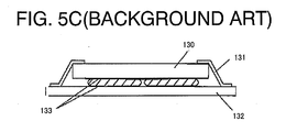
2002-176127 electronic component 130, and an electric circuit device. As shown inFIG. 5C , in addition to anelectric connection part 131 between theelectric component 130 and aboard 132, the electric circuit device has a thermally-conductive metal layer 133 between theelectric component 130 and theboard 132. Themetal layer 133 is separated into three or more sections with respect to the center of themetal layer 133. One or more side lines of each separated part are slightly rounded by chemical processing (plate processing). In this case, the use of chemical processing significantly increases the time for manufacturing the electric circuit device. - Presently, there is a need for a semiconductor device which has improved cooling performance, in other words, better thermal conductivity from a semiconductor element to a heat radiator, while minimizing the thermal stress.
- The present invention is directed to a semiconductor device. In accordance with one embodiment of the present invention, the semiconductor device includes a circuit board. The circuit board has an insulating substrate, a first metal plate fixed on a first side of the insulating substrate, and a second metal plate fixed on a second side of the insulating substrate. The semiconductor device further has a semiconductor element mounted on the first metal plate, a stress reducing member fixed on the second metal plate, and a heat cooling element fixed on the stress reducing member. The stress reducing member is plate-shaped and has at least one round-shaped corner.
- It is not intended that the invention be summarized here in its entirety. Rather, other aspects and advantages of the invention will become apparent from the following description, taken in conjunction with the accompanying drawings, illustrating by way of example the principles of the invention.
- The features of the present invention that are believed to be novel are set forth with particularity in the appended claims. The invention, together with objects and advantages thereof, may best be understood by reference to the following description of the embodiments together with the accompanying drawings in which:
-
FIG. 1 is a plan view illustrating a semiconductor device according to an embodiment of the present invention; -
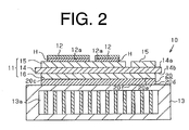
FIG. 2 is a cross-sectional view illustrating the semiconductor device that is taken along the line 2-2 inFIG.1 ; -
FIG. 3A is a plan view illustrating a stress reducing member of a semiconductor device according to an embodiment of the present invention; -
FIG. 3B is a cross-sectional view of the stress reducing member of the semiconductor device that is taken along theline 3B-3B inFIG.3A ; -
FIG. 4 is a plan view illustrating an alternative implementation of the present invention; -
FIG. 5A is a cross-sectional view illustrating a background art; -
FIG. 5B is a cross-sectional view illustrating another background art; and -
FIG. 5C is a cross-sectional view illustrating further other background art. - A semiconductor device according to an embodiment of the present invention will now be described with reference to
FIGS. 1 through 3 . - As shown in
FIG. 2 , asemiconductor device 10 has acircuit board 11,semiconductor elements 12 mounted on thecircuit board 11, and a heat sink 13 (i.e., a heat cooling element). Thecircuit board 11 has a plate-shaped ceramic substrate 14 (i.e., an insulating substrate), two metal circuits 15 (i.e., a first metal plate) fixed on thefirst side 14a of theceramic substrate 14, and a metal plate 16 (i.e., a second metal plate) fixed on thesecond side 14b of theceramic substrate 14. - The
heat sink 13 is fixed to theceramic substrate 14 through themetal plate 16 and astress reducing member 20. Theceramic substrate 14 is formed of a electrically insulating material, such as aluminum nitride, aluminium oxide or silicon nitride. Themetal circuits 15, themetal plate 16 and theheat sink 13 are formed of a good thermal conductor, such as aluminum, aluminum alloys or copper. - As shown in
FIGS. 1 and2 , thesemiconductor elements 12 are mounted on themetal circuits 15 through solder layer H. Twosemiconductor elements 12 are mounted on eachmetal circuit 15. Thesemiconductor elements 12 are electronic components, such as an IGBT (Insulated Gate Bipolar Transistor), MOSFET or diode. - As shown in
FIG. 2 , in order to guide the flow of a fluid such as a coolant,passages 13a are formed inside of theheat sink 13. - The
stress reducing member 20 is intervened between theheat sink 13 and themetal plate 16. The plate-shapedstress reducing member 20 is formed of a material having a high thermal conductivity, such as aluminum. Afirst side 20e of thestress reducing member 20faces bond surfaces 12a of thesemiconductor elements 12 to themetal circuits 15. The entirety of thefirst side 20e is brazed to themetal plate 16, and the entirety of thesecond side 20f of thestress reducing member 20 is brazed to theheat sink 13. Thecircuit board 11 and theheat sink 13 are connected through thestress reducing member 20, so that heat generated by thesemiconductor elements 12 is conducted to theheat sink 13 through thecircuit board 11 and thestress reducing member 20. - The
stress reducing member 20 will now be specifically described. InFIG. 3A , thesemiconductor elements 12, theceramic substrate 14 and themetal plate 16 are drawn by two-dot chain line. Afirst side line 20a and asecond side line 20b of thestress reducing member 20 face each other in a top-and-bottom direction, and athird side line 20c and afourth side line 20d of thestress reducing member 20 face each other in a left-and-right direction. A surrounding edge-portion of thestress reducing member 20 is formed by theside lines first side line 20a and thefourth side line 20d, thesecond side line 20b and thefourth side line 20d, thesecond side line 20b and thethird side line 20c, or thefirst side line 20a and thethird side line 20c) forming each corner C are connected together by an arc. - In this embodiment, the
stress reducing member 20 is in the shape of a square 30mm on a side line. Thestress reducing member 20 has the substantially same plan shape and size as themetal plate 16. The corners C are rounded in the shape of an arc, preferably, 3.5mm to 10mm (more preferably 3.5mm to 5mm) in diameter. Thermal stress tends to accumulate at a corner. Therefore, if the diameter is less than 3.5mm, it is insufficient to reduce thermal stress. On the other hand, if the diameter is more than 10mm, each bond surface of thestress reducing member 20 to themetal plate 16 and theheat sink 13 decreases, such that it is insufficient to conduct the heat generated by thesemiconductor elements 12 from themetal plate 16 to theheat sink 13. Note that, if tangential line M1 is drawn on any point of the line forming the corners C, tangential line M1 does not pass through the stress reducing member 20 (refer toFIG. 3A ). - The
stress reducing member 20 is brazed to themetal plate 16 and theheat sink 13 by a brazing filler metal. The brazing filler metal is in the shape of a sheet which has the same flat shape as thestress reducing member 20. In other words, corners of the brazing filler metal are rounded. - The surrounding edge-portion, other than the corners C, of the
stress reducing member 20 is co-extensive with a surrounding edge-portion of themetal plate 16. As shown inFIG. 3B , in the horizontal direction, the corners C are placed more inward thancorners 16a of themetal plate 16. Each corner C andcorresponding corner 16a form a step-structure together in the direction of the thickness of thecircuit board 11. Each corner C is directly under themetal plate 16 and directly above theheat sink 13. Thus, a stress reducing space S is formed by themetal plate 16, theheat sink 13 and the corners C. - As shown in
FIG. 3A , line L1 passes through each midpoint of thefirst side line 20a and thesecond side line 20b. Line L2 passes through each midpoint of thethird side line 20c and thefourth side line 20d. The corner C formed between thefirst side line 20a and thethird side line 20c, is symmetrical about line L2 with the corner C formed between thesecond side line 20b and thethird side line 20c. The corner C formed between thefirst side line 20a and thefourth side line 20d, is symmetrical about line L2 with the corner C formed between thesecond side line 20b and thefourth side line 20d. The corner C formed between thefirst side line 20a and thethird side line 20c, is symmetrical about line L1 with the corner C formed between thefirst side line 20a and thefourth side line 20d. The corner C formed between thesecond side line 20b and thethird side line 20c, is symmetrical about line L1 with the corner C formed between thesecond side line 20b and thefourth side line 20d. - Lines L3 and L4 each represent a diagonal line, which passes through two corners C, of the
stress reducing member 20. The corner C formed between thefirst side line 20a and thefourth side line 20d, is symmetrical about line L3 with the corner C formed between thesecond side line 20b and thethird side line 20c. The corner C formed between thefirst side line 20a and thethird side line 20c, is symmetrical about line L4 with the corner C formed between thesecond side line 20b and thefourth side line 20d. - When the above-mentioned
semiconductor device 10 is applied to, for example, a control circuit for controlling power provided to a car motor, thesemiconductor device 10 controls power according to car driving conditions. In this case, heat generated by thesemiconductor elements 12 is conducted to theheat sink 13 through themetal circuit 15, theceramic substrate 14, themetal plate 16 and thestress reducing member 20. The heat, which has been conducted to theheat sink 13, is removed by the fluid flowing through thepassages 13a in theheat sink 13. In other words, theheat sink 13 is cooled by the fluid. Thus, the heat is efficiently removed, and thesemiconductor elements 12 are cooled. - As heat is conducted to the
heat sink 13, the temperatures of theceramic substrate 14 and theheat sink 13 become elevated, resulting in the thermal expansion of both theceramic substrate 14 and theheat sink 13. On the other hand, when thesemiconductor elements 12 cease generating heat, the temperatures of theceramic substrate 14 and theheat sink 13 sink decrease, resulting in the thermal contraction of both theceramic substrate 14 and theheat sink 13. In expanding and contracting with heat, thermal stress arises from a difference in the linear expansion coefficients of theceramic substrate 14 and theheat sink 13. However, all corners C of thestress reducing member 20 are rounded, so that thermal stress affecting the corners C is reduced. Furthermore, when thermal stress arises, thestress reducing member 20 may be deformed in the stress reducing space S formed between thecorners 16a and theheat sink 13, thereby reducing the thermal stress. Therefore, cracking is prevented from arising between thestress reducing member 20 and themetal plate 16, as well as between thestress reducing member 20 and theheat sink 13. Warpage of the bond surface of theheat sink 13 to thecircuit board 11 is also prevented. - According to the embodiment of the invention, it is possible to bring about the following effects.
- Even if thermal stress arises from a difference in the linear expansion coefficients of the
ceramic substrate 14 and theheat sink 13, thestress reducing member 20 may be deformed in the stress reducing space S, so that thermal stress is reduced. Furthermore, the corners C are rounded, so that thermal stress on the corners C is more reduced compared to that on a sharp corner as shown in Japanese Unexamined Patent Publication No.2006-294699 stress reducing member 20 and themetal plate 16, as well as between thestress reducing member 20 and theheat sink 13. Warpage is also prevented from arising on theheat sink 13. - The corners C are rounded by pressing the material having the high thermal conductivity. Thus, the
stress reducing member 20 can be easily produced in a short time. Therefore, thesemiconductor device 10 can be produced in a short time. Where the corners are rounded by way of chemical processing (see, for example, Japanese Unexamined Patent Publication No.2002-176127 - The entirety of the first side of the
stress reducing member 20 is fixed on themetal plate 16, which resulting in improved conduction of heat from thestress reducing member 20 to theheat sink 13. Where thestress reducing member 20 is not wholly fixed on the metal plate 16 (see, for example,FIG. 5B in which stressrelaxation member 125 has stress relaxation holes 126 thereon), that benefit is not achieved. - When thermal stress is added to the
stress reducing member 20, thestress reducing member 20 may be deformed in the stress reducing space S, so that thermal stress can be reduced. - The surrounding edge-portion, other than the corners C, of the
stress reducing member 20 is co-extensive with the surrounding edge-portion of themetal plate 16. Thus, thermal conductivity from themetal plate 16 to thestress reducing member 20 is prevented from decreasing, even though the corners C are rounded, resulting in a decreased area for conducting the heat from themetal plate 16 to thestress reducing member 20. - Each corner C is symmetrical about either the line L1, L2, L3 or L4. Therefore, thermal stress is distributed equally to the surrounding edge-portion of the
stress reducing member 20. In other words, thermal stress is prevented from being concentrated to any portion of the stress reducing memeber20. - In the present invention, the following alternative implementations are also encompassed.
- In an alternative embodiment to the preferred embodiment, as shown in
FIG. 3A , recesses or throughholes 22 are formed on the first side of thestress reducing member 20. - In an alternative embodiment to the preferred embodiment, the
stress reducing member 20 has a flat shape smaller than that of themetal plate 16. In other words, thestress reducing member 20 is placed inside the surrounding edge-portion of themetal plate 16. - In another alternative embodiment to the preferred embodiment, the shape of corner C is not limited to the arc mentioned above. As shown in
FIG. 4 , thestress reducing member 20 hascorners 20k which are made clipped by straightly planning them off. Also, it is not necessary that the corner C is symmetric with corresponding other corner C with respect to either line L1, L2, L3 or L4. In brief, any corner C is adopted as the round-shaped corner, as long as the corner C is of more obtuse than thecorners 16a of themetal plate 16. - In a further alternative embodiment to the preferred embodiment, only one, two or three of the corners C are rounded.
- In the above-described preferred embodiment, water is adopted as a fluid flowing through the
heat sink 13. In an alternative embodiment to the preferred embodiment, however, another liquid or air is adopted. - In an alternative embodiment to the preferred embodiment, a boiling-cooled-type heat sink is adopted as the heat radiator.
- In another alternative embodiment to the preferred embodiment, one, or more than two
metal circuits 15 are placed on thecircuit board 11. Also, one, or more than twosemiconductor elements 12 are placed on thecircuit board 11. - In a further alternative embodiment to the preferred embodiment, the
semiconductor device 10 can be applied to other than the control circuit on the car. - Therefore, the present examples and embodiments are to be considered as illustrative and not restrictive and the invention is not to be limited to the details given herein but may be modified within the scope of the appended claims.
- This application claims a foreign priority benefit based on Japanese Patent Application No.
2007- 139032, filed on May 25, 2007 - The semiconductor device includes a circuit board. The circuit board has an insulating substrate, a metal circuit fixed on a first side of the insulating substrate, and a metal plate fixed on a second side of the insulating substrate. The semiconductor device further has a semiconductor element mounted on the metal circuit, a stress reducing member fixed on the metal plate, and a heat sink fixed on the stress reducing member. The stress reducing member is plate-shaped and has round-shaped corners.
Claims (9)
- A semiconductor device (10), comprising:a circuit board (11) including an insulating substrate (14), a first metal plate (15) fixed on a first side of (14a) the insulating substrate (14), and a second metal plate (16) fixed on a second side (14b) of the insulating substrate (14);a semiconductor element (12) mounted on the first metal plate (15);a stress reducing member (20) fixed on the second metal plate (16); anda heat cooling element (13) fixed on the stress reducing member (20),characterized in thatthe stress reducing member (20) is plate-shaped and have a round-shaped corner (C).
- The semiconductor device (10) of claim 1, wherein the stress reducing member (20) is formed of a material having a high thermal conductivity, and the corner (C) is rounded by press working.
- The semiconductor device (10) of any one of claims 1 and 2, wherein a first side (20e) of the stress reducing member (20) faces a bond surface (12a) of the semiconductor element (12) to the first metal plate (15), and the entirety of the first side (20e) of the stress reducing member (20) is fixed on the second metal plate (16).
- The semiconductor device (10) of any one of claims 1 through 3, wherein the corner (C) of the stress reducing member (20) and corresponding corner (C) of the second metal plate (16) form a step-structure together in the direction of the thickness of the circuit board (11).
- The semiconductor device (10) of claim 4, wherein a surrounding edge-portion, other than the corner (C), of the stress reducing member (20) is co-extensive with a surrounding edge-portion of the second metal plate (16).
- The semiconductor device (10) of any one of claims 1 through 5, wherein a first side (20e) of the stress reducing member (20) faces a bond surface (12a) of the semiconductor element (12) to the first metal plate (15), and a recess (22) is formed on the first side (20e) of the stress reducing member (20).
- The semiconductor device (10) of any one of claims 1 through 6, wherein the stress reducing member (20) is in the shape of a square having four side lines (20a, 20b, 20c and 20d), and a standard line (L1) passes through each midpoint of the first side line (20a) and the facing second side line (20b), and the round-shaped corner (C) formed between the first side line (20a) and the third side line (20c) is symmetrical about the standard line (L1) with another round-shaped corner (C) formed between the first side line (20a) and the fourth side line (20d).
- The semiconductor device (10) of any one of claims 1 through 7, wherein the stress reducing member (20) is in the shape of a square having four side lines (20a, 20b, 20c and 20d), and the round-shaped corner (C) formed between the first side line (20a) and the adjoining fourth side line (20d) is symmetrical with another round-shaped corner (C) formed between the second side line (20b) and the third side line (20c), about a diagonal line connecting the rest two corners (C).
- A method for manufacturing a semiconductor device (10), comprising the steps of:fixing a first metal plate (15) on the first side (14a) of an insulating substrate (14);fixing a second metal plate (16) on the second side (14b) of the insulating substrate (14);mounting a semiconductor element (12) on the first metal plate (15);fixing a stress reducing member (20) on the second metal plate (16); andfixing a heat cooling element (13) on the stress reducing member (20),characterized in thatrounding a corner (C) of the stress reducing member (20) by press working, wherein the stress reducing member (20) is plate-shaped, and is formed of a material having a high thermal conductivity.
Applications Claiming Priority (1)
| Application Number | Priority Date | Filing Date | Title |
|---|---|---|---|
| JP2007139032A JP4867793B2 (en) | 2007-05-25 | 2007-05-25 | Semiconductor device |
Publications (3)
| Publication Number | Publication Date |
|---|---|
| EP1995775A2 true EP1995775A2 (en) | 2008-11-26 |
| EP1995775A3 EP1995775A3 (en) | 2010-01-13 |
| EP1995775B1 EP1995775B1 (en) | 2015-11-04 |
Family
ID=39686414
Family Applications (1)
| Application Number | Title | Priority Date | Filing Date |
|---|---|---|---|
| EP08156826.3A Ceased EP1995775B1 (en) | 2007-05-25 | 2008-05-23 | Semiconductor device with stress reducing element |
Country Status (5)
| Country | Link |
|---|---|
| US (1) | US7813135B2 (en) |
| EP (1) | EP1995775B1 (en) |
| JP (1) | JP4867793B2 (en) |
| KR (1) | KR20080103913A (en) |
| CN (1) | CN101312183B (en) |
Families Citing this family (33)
| Publication number | Priority date | Publication date | Assignee | Title |
|---|---|---|---|---|
| JP5070014B2 (en) * | 2007-11-21 | 2012-11-07 | 株式会社豊田自動織機 | Heat dissipation device |
| JP2009130060A (en) * | 2007-11-21 | 2009-06-11 | Toyota Industries Corp | Heat dissipation device |
| JP5163199B2 (en) * | 2008-03-17 | 2013-03-13 | 三菱マテリアル株式会社 | Power module substrate with heat sink and power module with heat sink |
| US8472193B2 (en) | 2008-07-04 | 2013-06-25 | Kabushiki Kaisha Toyota Jidoshokki | Semiconductor device |
| JP5546889B2 (en) * | 2010-02-09 | 2014-07-09 | 日本電産エレシス株式会社 | Electronic component unit and manufacturing method thereof |
| JP5525856B2 (en) * | 2010-02-24 | 2014-06-18 | 株式会社豊田中央研究所 | Semiconductor module |
| JP5565147B2 (en) * | 2010-06-30 | 2014-08-06 | 株式会社デンソー | Manufacturing method of semiconductor module |
| JP5349572B2 (en) * | 2011-04-18 | 2013-11-20 | 株式会社豊田自動織機 | Radiator and method of manufacturing radiator |
| JP2013026279A (en) * | 2011-07-15 | 2013-02-04 | Showa Denko Kk | Insulation laminate material, base for power module and power module |
| CN104137252B (en) * | 2012-02-22 | 2017-07-14 | 三菱电机株式会社 | The manufacture method of semiconductor device and semiconductor device |
| US8940618B2 (en) * | 2012-03-13 | 2015-01-27 | Taiwan Semiconductor Manufacturing Company, Ltd. | Method and device for cutting semiconductor wafers |
| JP2014011435A (en) * | 2012-07-03 | 2014-01-20 | Nippon Steel & Sumikin Electronics Devices Inc | Ceramic composite substrate |
| CN104704629A (en) * | 2012-10-16 | 2015-06-10 | 富士电机株式会社 | Cooling structure and heat generating body |
| US8872328B2 (en) * | 2012-12-19 | 2014-10-28 | General Electric Company | Integrated power module package |
| US9470720B2 (en) | 2013-03-08 | 2016-10-18 | Sandisk Technologies Llc | Test system with localized heating and method of manufacture thereof |
| US10013033B2 (en) | 2013-06-19 | 2018-07-03 | Sandisk Technologies Llc | Electronic assembly with thermal channel and method of manufacture thereof |
| US9898056B2 (en) | 2013-06-19 | 2018-02-20 | Sandisk Technologies Llc | Electronic assembly with thermal channel and method of manufacture thereof |
| US9313874B2 (en) * | 2013-06-19 | 2016-04-12 | SMART Storage Systems, Inc. | Electronic system with heat extraction and method of manufacture thereof |
| US9867282B2 (en) * | 2013-08-16 | 2018-01-09 | Ati Technologies Ulc | Circuit board with corner hollows |
| US9158349B2 (en) | 2013-10-04 | 2015-10-13 | Sandisk Enterprise Ip Llc | System and method for heat dissipation |
| US9549457B2 (en) | 2014-02-12 | 2017-01-17 | Sandisk Technologies Llc | System and method for redirecting airflow across an electronic assembly |
| US9497889B2 (en) | 2014-02-27 | 2016-11-15 | Sandisk Technologies Llc | Heat dissipation for substrate assemblies |
| US9348377B2 (en) | 2014-03-14 | 2016-05-24 | Sandisk Enterprise Ip Llc | Thermal isolation techniques |
| US9519319B2 (en) | 2014-03-14 | 2016-12-13 | Sandisk Technologies Llc | Self-supporting thermal tube structure for electronic assemblies |
| US9485851B2 (en) | 2014-03-14 | 2016-11-01 | Sandisk Technologies Llc | Thermal tube assembly structures |
| JP6278516B2 (en) * | 2014-05-28 | 2018-02-14 | Ngkエレクトロデバイス株式会社 | Power module substrate |
| JP6033522B1 (en) | 2014-12-18 | 2016-11-30 | 三菱電機株式会社 | Insulated circuit board, power module and power unit |
| JP7039917B2 (en) * | 2017-10-06 | 2022-03-23 | 富士電機株式会社 | Cooler |
| DE102018205243A1 (en) * | 2018-04-09 | 2019-10-10 | Zf Friedrichshafen Ag | Electronic power control module and method of manufacturing an electronic power control module |
| EP3588525B1 (en) | 2018-06-28 | 2022-02-16 | Black & Decker Inc. | Electronic switch module with oppositely-arranged power switches and discrete heat sinks |
| US10490482B1 (en) * | 2018-12-05 | 2019-11-26 | Toyota Motor Engineering & Manufacturing North America, Inc. | Cooling devices including jet cooling with an intermediate mesh and methods for using the same |
| CN111465169A (en) * | 2020-03-25 | 2020-07-28 | 万安裕维电子有限公司 | Anti-warping PCB |
| CN113223410A (en) * | 2021-04-27 | 2021-08-06 | 武汉华星光电半导体显示技术有限公司 | Display panel and electronic device |
Citations (4)
| Publication number | Priority date | Publication date | Assignee | Title |
|---|---|---|---|---|
| JP2002176127A (en) | 2000-12-06 | 2002-06-21 | Hitachi Ltd | Electronic component cooling structure and electronic circuit device having this cooling structure |
| JP2004153075A (en) | 2002-10-31 | 2004-05-27 | Mitsubishi Materials Corp | Power module substrate and power module |
| JP2006294699A (en) | 2005-04-06 | 2006-10-26 | Toyota Industries Corp | Heat dissipation device |
| JP2007139032A (en) | 2005-11-16 | 2007-06-07 | Ogura Clutch Co Ltd | Electromagnetic coupling device |
Family Cites Families (31)
| Publication number | Priority date | Publication date | Assignee | Title |
|---|---|---|---|---|
| JPH0765567B2 (en) | 1986-04-09 | 1995-07-19 | 株式会社豊田自動織機製作所 | Control Mechanism of Crank Chamber Pressure in Oscillating Swash Plate Compressor |
| JPS6459986A (en) * | 1987-08-31 | 1989-03-07 | Toshiba Corp | Ceramic circuit board |
| JP2699517B2 (en) * | 1988-02-24 | 1998-01-19 | モトローラ・インコーポレーテッド | Semiconductor device having round or tapered edges and corners |
| DE4004844C1 (en) | 1990-02-16 | 1991-01-03 | Abb Ixys Semiconductor Gmbh | Copper metallisation on ceramic substrate - obtd. by bonding copper foil directly to whole surface of substrate, then masking and etching |
| JPH0529509A (en) * | 1991-07-23 | 1993-02-05 | Toshiba Corp | Substrate for semiconductor |
| JPH05166969A (en) | 1991-10-14 | 1993-07-02 | Fuji Electric Co Ltd | Semiconductor device |
| JP2629635B2 (en) * | 1995-02-23 | 1997-07-09 | 日本電気株式会社 | Semiconductor device with metal plate for heat dissipation |
| JPH0955459A (en) * | 1995-06-06 | 1997-02-25 | Seiko Epson Corp | Semiconductor device |
| DE69728919T2 (en) | 1996-02-07 | 2005-04-14 | Hitachi, Ltd. | Circuit board and semiconductor device with this |
| JPH104156A (en) * | 1996-06-14 | 1998-01-06 | Mitsubishi Electric Corp | Insulating substrate for semiconductor device and semiconductor device |
| JPH1117081A (en) | 1997-06-19 | 1999-01-22 | Sansha Electric Mfg Co Ltd | Power semiconductor module |
| JP2002198468A (en) | 2000-12-26 | 2002-07-12 | Sumitomo Metal Electronics Devices Inc | Semiconductor module |
| JP4969738B2 (en) | 2001-06-28 | 2012-07-04 | 株式会社東芝 | Ceramic circuit board and semiconductor module using the same |
| JP3726759B2 (en) | 2002-02-18 | 2005-12-14 | 株式会社豊田自動織機 | Control device for variable capacity compressor |
| JP2003289191A (en) * | 2002-03-28 | 2003-10-10 | Denso Corp | Electronic control unit |
| US6844621B2 (en) * | 2002-08-13 | 2005-01-18 | Fuji Electric Co., Ltd. | Semiconductor device and method of relaxing thermal stress |
| JP2004327648A (en) | 2003-04-24 | 2004-11-18 | Fujitsu Ltd | Electronic component mounting method, mounting structure and package substrate |
| JP4276881B2 (en) | 2003-04-30 | 2009-06-10 | 日本圧着端子製造株式会社 | Multilayer printed wiring board connection structure |
| JP2005009422A (en) | 2003-06-19 | 2005-01-13 | Toyota Industries Corp | Capacity control mechanism for variable displacement compressor |
| JP2005032833A (en) * | 2003-07-08 | 2005-02-03 | Toshiba Corp | Module type semiconductor device |
| JP2006240955A (en) | 2005-03-07 | 2006-09-14 | Denki Kagaku Kogyo Kk | Ceramic substrate, ceramic circuit substrate and power control component using the same. |
| JP2006351988A (en) * | 2005-06-20 | 2006-12-28 | Denki Kagaku Kogyo Kk | Ceramic substrate, ceramic circuit substrate and power control component using the same. |
| JP4617209B2 (en) * | 2005-07-07 | 2011-01-19 | 株式会社豊田自動織機 | Heat dissipation device |
| US7195145B2 (en) * | 2005-07-13 | 2007-03-27 | Motorola, Inc. | Electrical circuit apparatus and method for assembling same |
| JP4759384B2 (en) * | 2005-12-20 | 2011-08-31 | 昭和電工株式会社 | Semiconductor module |
| DE102006014609B4 (en) * | 2006-03-29 | 2021-03-18 | Infineon Technologies Ag | Semiconductor component carriers |
| JP4945319B2 (en) * | 2007-05-25 | 2012-06-06 | 昭和電工株式会社 | Semiconductor device |
| JP2008294279A (en) * | 2007-05-25 | 2008-12-04 | Showa Denko Kk | Semiconductor device |
| JP2008294280A (en) * | 2007-05-25 | 2008-12-04 | Showa Denko Kk | Semiconductor device |
| JP5070014B2 (en) * | 2007-11-21 | 2012-11-07 | 株式会社豊田自動織機 | Heat dissipation device |
| JP2009130060A (en) * | 2007-11-21 | 2009-06-11 | Toyota Industries Corp | Heat dissipation device |
-
2007
- 2007-05-25 JP JP2007139032A patent/JP4867793B2/en not_active Expired - Fee Related
-
2008
- 2008-05-23 KR KR1020080047857A patent/KR20080103913A/en not_active Ceased
- 2008-05-23 US US12/154,592 patent/US7813135B2/en not_active Expired - Fee Related
- 2008-05-23 EP EP08156826.3A patent/EP1995775B1/en not_active Ceased
- 2008-05-23 CN CN2008101277162A patent/CN101312183B/en not_active Expired - Fee Related
Patent Citations (4)
| Publication number | Priority date | Publication date | Assignee | Title |
|---|---|---|---|---|
| JP2002176127A (en) | 2000-12-06 | 2002-06-21 | Hitachi Ltd | Electronic component cooling structure and electronic circuit device having this cooling structure |
| JP2004153075A (en) | 2002-10-31 | 2004-05-27 | Mitsubishi Materials Corp | Power module substrate and power module |
| JP2006294699A (en) | 2005-04-06 | 2006-10-26 | Toyota Industries Corp | Heat dissipation device |
| JP2007139032A (en) | 2005-11-16 | 2007-06-07 | Ogura Clutch Co Ltd | Electromagnetic coupling device |
Also Published As
| Publication number | Publication date |
|---|---|
| EP1995775B1 (en) | 2015-11-04 |
| JP2008294284A (en) | 2008-12-04 |
| JP4867793B2 (en) | 2012-02-01 |
| CN101312183A (en) | 2008-11-26 |
| EP1995775A3 (en) | 2010-01-13 |
| US20080291636A1 (en) | 2008-11-27 |
| CN101312183B (en) | 2011-05-18 |
| US7813135B2 (en) | 2010-10-12 |
| KR20080103913A (en) | 2008-11-28 |
Similar Documents
| Publication | Publication Date | Title |
|---|---|---|
| US7813135B2 (en) | Semiconductor device | |
| KR101215695B1 (en) | Heat dissipation device and power module | |
| KR101384426B1 (en) | Base for power module | |
| KR101188150B1 (en) | Cooling system | |
| US11062972B2 (en) | Electronic module for power control and method for manufacturing an electronic module power control | |
| JP6257478B2 (en) | Power semiconductor device | |
| CN110047807B (en) | Semiconductor device | |
| JPH09329395A (en) | heatsink | |
| KR101461329B1 (en) | Semiconductor unit | |
| JP2004022973A (en) | Ceramic circuit board and semiconductor module | |
| JP2008311550A (en) | Power semiconductor module | |
| JP2026071271A (en) | Ceramic circuit board, semiconductor device, and method of using the semiconductor device | |
| JP2008294281A (en) | Semiconductor device and manufacturing method of semiconductor device | |
| JP4968150B2 (en) | Semiconductor element cooling device | |
| JP4935783B2 (en) | Semiconductor device and composite semiconductor device | |
| JP2004235175A (en) | Power semiconductor module | |
| JP2007096252A (en) | Liquid-cooled circuit board and liquid-cooled electronic device | |
| JP2009224556A (en) | Printing plate, and attachment method of power module using it |
Legal Events
| Date | Code | Title | Description |
|---|---|---|---|
| PUAI | Public reference made under article 153(3) epc to a published international application that has entered the european phase |
Free format text: ORIGINAL CODE: 0009012 |
|
| 17P | Request for examination filed |
Effective date: 20080523 |
|
| AK | Designated contracting states |
Kind code of ref document: A2 Designated state(s): AT BE BG CH CY CZ DE DK EE ES FI FR GB GR HR HU IE IS IT LI LT LU LV MC MT NL NO PL PT RO SE SI SK TR |
|
| AX | Request for extension of the european patent |
Extension state: AL BA MK RS |
|
| PUAL | Search report despatched |
Free format text: ORIGINAL CODE: 0009013 |
|
| AK | Designated contracting states |
Kind code of ref document: A3 Designated state(s): AT BE BG CH CY CZ DE DK EE ES FI FR GB GR HR HU IE IS IT LI LT LU LV MC MT NL NO PL PT RO SE SI SK TR |
|
| AX | Request for extension of the european patent |
Extension state: AL BA MK RS |
|
| RIC1 | Information provided on ipc code assigned before grant |
Ipc: H05K 3/00 20060101ALI20091208BHEP Ipc: H01L 23/473 20060101ALI20091208BHEP Ipc: H01L 23/538 20060101ALI20091208BHEP Ipc: H01L 23/373 20060101AFI20080821BHEP Ipc: H05K 1/02 20060101ALI20091208BHEP |
|
| AKX | Designation fees paid |
Designated state(s): DE FR IT |
|
| 17Q | First examination report despatched |
Effective date: 20130405 |
|
| GRAP | Despatch of communication of intention to grant a patent |
Free format text: ORIGINAL CODE: EPIDOSNIGR1 |
|
| INTG | Intention to grant announced |
Effective date: 20150129 |
|
| GRAS | Grant fee paid |
Free format text: ORIGINAL CODE: EPIDOSNIGR3 |
|
| GRAA | (expected) grant |
Free format text: ORIGINAL CODE: 0009210 |
|
| AK | Designated contracting states |
Kind code of ref document: B1 Designated state(s): DE FR IT |
|
| REG | Reference to a national code |
Ref country code: DE Ref legal event code: R096 Ref document number: 602008040961 Country of ref document: DE |
|
| REG | Reference to a national code |
Ref country code: FR Ref legal event code: PLFP Year of fee payment: 9 |
|
| REG | Reference to a national code |
Ref country code: DE Ref legal event code: R097 Ref document number: 602008040961 Country of ref document: DE |
|
| PLBE | No opposition filed within time limit |
Free format text: ORIGINAL CODE: 0009261 |
|
| STAA | Information on the status of an ep patent application or granted ep patent |
Free format text: STATUS: NO OPPOSITION FILED WITHIN TIME LIMIT |
|
| 26N | No opposition filed |
Effective date: 20160805 |
|
| REG | Reference to a national code |
Ref country code: FR Ref legal event code: PLFP Year of fee payment: 10 |
|
| PGFP | Annual fee paid to national office [announced via postgrant information from national office to epo] |
Ref country code: DE Payment date: 20170516 Year of fee payment: 10 Ref country code: FR Payment date: 20170413 Year of fee payment: 10 |
|
| PGFP | Annual fee paid to national office [announced via postgrant information from national office to epo] |
Ref country code: IT Payment date: 20170522 Year of fee payment: 10 |
|
| REG | Reference to a national code |
Ref country code: DE Ref legal event code: R119 Ref document number: 602008040961 Country of ref document: DE |
|
| PG25 | Lapsed in a contracting state [announced via postgrant information from national office to epo] |
Ref country code: DE Free format text: LAPSE BECAUSE OF NON-PAYMENT OF DUE FEES Effective date: 20181201 Ref country code: IT Free format text: LAPSE BECAUSE OF NON-PAYMENT OF DUE FEES Effective date: 20180523 Ref country code: FR Free format text: LAPSE BECAUSE OF NON-PAYMENT OF DUE FEES Effective date: 20180531 |