EP1988336A1 - Illuminating apparatus - Google Patents
Illuminating apparatus Download PDFInfo
- Publication number
- EP1988336A1 EP1988336A1 EP07714482A EP07714482A EP1988336A1 EP 1988336 A1 EP1988336 A1 EP 1988336A1 EP 07714482 A EP07714482 A EP 07714482A EP 07714482 A EP07714482 A EP 07714482A EP 1988336 A1 EP1988336 A1 EP 1988336A1
- Authority
- EP
- European Patent Office
- Prior art keywords
- light emitting
- emitting device
- lighting fixture
- heat radiation
- fins
- Prior art date
- Legal status (The legal status is an assumption and is not a legal conclusion. Google has not performed a legal analysis and makes no representation as to the accuracy of the status listed.)
- Withdrawn
Links
Images







Classifications
-
- F—MECHANICAL ENGINEERING; LIGHTING; HEATING; WEAPONS; BLASTING
- F21—LIGHTING
- F21S—NON-PORTABLE LIGHTING DEVICES; SYSTEMS THEREOF; VEHICLE LIGHTING DEVICES SPECIALLY ADAPTED FOR VEHICLE EXTERIORS
- F21S2/00—Systems of lighting devices, not provided for in main groups F21S4/00 - F21S10/00 or F21S19/00, e.g. of modular construction
- F21S2/005—Systems of lighting devices, not provided for in main groups F21S4/00 - F21S10/00 or F21S19/00, e.g. of modular construction of modular construction
-
- F—MECHANICAL ENGINEERING; LIGHTING; HEATING; WEAPONS; BLASTING
- F21—LIGHTING
- F21S—NON-PORTABLE LIGHTING DEVICES; SYSTEMS THEREOF; VEHICLE LIGHTING DEVICES SPECIALLY ADAPTED FOR VEHICLE EXTERIORS
- F21S8/00—Lighting devices intended for fixed installation
- F21S8/04—Lighting devices intended for fixed installation intended only for mounting on a ceiling or the like overhead structures
-
- F—MECHANICAL ENGINEERING; LIGHTING; HEATING; WEAPONS; BLASTING
- F21—LIGHTING
- F21S—NON-PORTABLE LIGHTING DEVICES; SYSTEMS THEREOF; VEHICLE LIGHTING DEVICES SPECIALLY ADAPTED FOR VEHICLE EXTERIORS
- F21S8/00—Lighting devices intended for fixed installation
- F21S8/08—Lighting devices intended for fixed installation with a standard
- F21S8/085—Lighting devices intended for fixed installation with a standard of high-built type, e.g. street light
- F21S8/086—Lighting devices intended for fixed installation with a standard of high-built type, e.g. street light with lighting device attached sideways of the standard, e.g. for roads and highways
-
- F—MECHANICAL ENGINEERING; LIGHTING; HEATING; WEAPONS; BLASTING
- F21—LIGHTING
- F21V—FUNCTIONAL FEATURES OR DETAILS OF LIGHTING DEVICES OR SYSTEMS THEREOF; STRUCTURAL COMBINATIONS OF LIGHTING DEVICES WITH OTHER ARTICLES, NOT OTHERWISE PROVIDED FOR
- F21V29/00—Protecting lighting devices from thermal damage; Cooling or heating arrangements specially adapted for lighting devices or systems
- F21V29/50—Cooling arrangements
- F21V29/70—Cooling arrangements characterised by passive heat-dissipating elements, e.g. heat-sinks
- F21V29/74—Cooling arrangements characterised by passive heat-dissipating elements, e.g. heat-sinks with fins or blades
- F21V29/75—Cooling arrangements characterised by passive heat-dissipating elements, e.g. heat-sinks with fins or blades with fins or blades having different shapes, thicknesses or spacing
-
- F—MECHANICAL ENGINEERING; LIGHTING; HEATING; WEAPONS; BLASTING
- F21—LIGHTING
- F21V—FUNCTIONAL FEATURES OR DETAILS OF LIGHTING DEVICES OR SYSTEMS THEREOF; STRUCTURAL COMBINATIONS OF LIGHTING DEVICES WITH OTHER ARTICLES, NOT OTHERWISE PROVIDED FOR
- F21V29/00—Protecting lighting devices from thermal damage; Cooling or heating arrangements specially adapted for lighting devices or systems
- F21V29/50—Cooling arrangements
- F21V29/70—Cooling arrangements characterised by passive heat-dissipating elements, e.g. heat-sinks
- F21V29/74—Cooling arrangements characterised by passive heat-dissipating elements, e.g. heat-sinks with fins or blades
- F21V29/76—Cooling arrangements characterised by passive heat-dissipating elements, e.g. heat-sinks with fins or blades with essentially identical parallel planar fins or blades, e.g. with comb-like cross-section
- F21V29/763—Cooling arrangements characterised by passive heat-dissipating elements, e.g. heat-sinks with fins or blades with essentially identical parallel planar fins or blades, e.g. with comb-like cross-section the planes containing the fins or blades having the direction of the light emitting axis
-
- F—MECHANICAL ENGINEERING; LIGHTING; HEATING; WEAPONS; BLASTING
- F21—LIGHTING
- F21W—INDEXING SCHEME ASSOCIATED WITH SUBCLASSES F21K, F21L, F21S and F21V, RELATING TO USES OR APPLICATIONS OF LIGHTING DEVICES OR SYSTEMS
- F21W2131/00—Use or application of lighting devices or systems not provided for in codes F21W2102/00-F21W2121/00
- F21W2131/10—Outdoor lighting
- F21W2131/103—Outdoor lighting of streets or roads
-
- F—MECHANICAL ENGINEERING; LIGHTING; HEATING; WEAPONS; BLASTING
- F21—LIGHTING
- F21Y—INDEXING SCHEME ASSOCIATED WITH SUBCLASSES F21K, F21L, F21S and F21V, RELATING TO THE FORM OR THE KIND OF THE LIGHT SOURCES OR OF THE COLOUR OF THE LIGHT EMITTED
- F21Y2115/00—Light-generating elements of semiconductor light sources
- F21Y2115/10—Light-emitting diodes [LED]
Definitions
- the present invention relates to a lighting fixture in which multiple light emitting device modules are provided, each having fins for radiating heat generated by a light emitting device.
- a lighting fixture described in patent document 1 is equipped with multiple light emitting device modules (LED light-source modules) each having fins for radiating heat generated by a light emitting device (LED).
- LED light-source modules each having fins for radiating heat generated by a light emitting device (LED).
- the light emitting device (LED) is placed on the same surface as the surface where the fins are placed, among all the surfaces of a bridging part (base) for bridging roots of adjacent fins, and a housing of the lighting fixture is made to abut against the surface opposite to the surface where the fins are arranged.
- the heat generated from the light emitting device (LED) is radiated from the fins via the bridging part (base), and the heat is also conducted to the housing of the lighting fixture via the bridging part (base).
- multiple light emitting device modules (LED light source modules) are provided, and those multiple light emitting device modules are arranged in such a manner that a main optical axis line of one light emitting device module is parallel to the main optical axis of other light emitting device modules. Therefore, the light from the multiple light emitting device modules cannot illuminate multiple different directions.
- the present invention is to provide a lighting fixture which allows illumination from the light emitting device modules at wide angle in multiple different directions, while avoiding the deterioration of efficiency of the heat radiation by the fins.
- a lighting fixture provided with multiple light emitting device modules each including a light emitting device and fins for radiating heat generated by the light emitting device, wherein, all the multiple light emitting device modules are arranged in such a manner that a main optical axis line of one light emitting device module and a main optical axis line of other light emitting device module forms an angle of larger than zero degree, or those main optical axis lines are in skew position, and all the fins are arranged in such a manner that all the fins are parallel with respect to a vertical plane and roots of the fins are located at the same height as or lower than tips of the fins.
- the inventors of the present invention zealously studied at what part a covering layer is to be formed on a surface of a heat radiation member for radiating the heat generated by the light emitting device, in order to enhance efficiency at a maximum in cooling the light emitting device by the heat radiation member.
- the present inventors have found the followings: when the covering layer is formed on a part exposed to the air on the surface of the heat radiation member, the efficiency of the heat radiation from the heat radiation member toward the air can be improved, resulting in that the efficiency for cooling the light emitting device by the heat radiation member can be enhanced.
- the covering layer is formed on a part being in contact with the light emitting device on the surface of the heat radiation member, heat transfer resistance between the light emitting device and the heat radiation member is increased, resulting in that the efficiency for cooling the light emitting device by the heat radiation member is deteriorated.
- the present inventors have found that the efficiency for cooling the light emitting device by the heat radiation member is more enhanced, when the covering layer is not formed at the part which is in contact with the light emitting device on the surface of the heat radiation member.
- the present inventors have found that if polishing is performed at a part which comes into contact with the light emitting device on the surface of the heat radiation member, rather than leaving the part as a solid surface, the heat transfer resistance can be reduced, resulting in that the efficiency for cooling the light emitting device by the heat radiation member is more enhanced.
- the present inventors have found that if a grease-like or a sheet-like thermally conductive interface material is placed on the part which comes into contact with the light emitting device on the surface of the heat radiation member, rather than leaving the part as a solid surface, the heat transfer resistance can be reduced, resulting in that the efficiency for cooling the light emitting device by the heat radiation member is more enhanced.
- the present inventors zealously studied the cooling efficiency of the light emitting device, not only in the case where the light emitting device is directly connected with the heat radiation member but also in the case where the light emitting device is connected with the heat radiation member via the heat transfer member.
- the present inventors have found that when a covering layer is formed at a part which is exposed to the air on the surface of the heat transfer member, the heat radiation efficiency from the heat transfer member into the air can be enhanced, resulting in that the efficiency for cooling the light emitting device by the heat transfer member may be improved. That is, the heat transfer member is found to function as the heat radiation member.
- the present inventors have found that if the covering layer is formed on a part which is in contact with the light emitting device and on a part which is in contact with the heat radiation member, on the surface of the heat transfer member, the heat transfer resistance is increased, resulting in that the efficiency for cooling the light emitting device is deteriorated.
- the present inventors have found that it is better not to form the covering layer at the part being in contact with the light emitting device and at the part being in contact with the heat radiation member, on the surface of the heat transfer member, in order to enhance the efficiency for cooling the light emitting device.
- the present inventors have found that if polishing is performed at the part being in contact with the light emitting device and the part being in contact with the heat radiation member, on the surface of the heat transfer member, rather than leaving the parts as solid surfaces, the heat transfer resistance can be reduced, resulting in that the efficiency for cooling the light emitting device by the heat radiation member is more enhanced.
- the present inventors have found that if the thermally conductive interface material is placed at the part being in contact with the light emitting device and at the part being in contact with the heat radiation member, on the surface of the heat transfer member, rather than leaving the parts as solid surfaces, the heat transfer resistance can be reduced, resulting in that the efficiency for cooling the light emitting device by the heat radiation member is more enhanced.
- the present inventors zealously studied which part is to be subjected to a roughening process on the surface of the heat radiation member for radiating the heat generated by the light emitting device, in order to enhance the efficiency at a maximum, in cooling the light emitting device by the heat radiation member.
- the present inventors have found the followings: when the roughening process is performed at the part exposed to the air on the surface of the heat radiation member, the efficiency of the heat radiation from the heat radiation member towards the air can be improved, resulting in that the efficiency for cooling the light emitting device by the heat radiation member can be enhanced.
- the roughening process is performed at the part being in contact with to the light emitting device on the surface of the heat radiation member, a heat transfer resistance between the light emitting device and the heat radiation member is increased, resulting in that the efficiency for cooling the light emitting device by the heat radiation member is deteriorated.
- the present inventors have found that it is better not to perform the roughening process at the part being in contact with the light emitting device on the surface of the heat radiation member, in order to enhance the efficiency for cooling the light emitting device by the heat radiation member.
- multiple light emitting device modules are arranged in such a manner that a main optical axis line of one light emitting device module and a main optical axis line of other light emitting device module form an angle of larger than zero degree, or those main optical axis lines are in skew position. Therefore, the multiple light emitting device modules are allowed to illuminate multiple different directions.
- all the fins are arranged in such a manner the all the fins are parallel with respect to the vertical plane, and the roots of the fins are located at the same height as or lower level than the tips of the fins. Therefore, the above problems 1 and 2 are solved, and accordingly, deterioration the efficiency of heat radiation by the fins can be avoided.
- the lighting fixture of the present invention allows the multiple light emitting device modules to illuminate the multiple different directions, while avoiding deterioration of radiation efficiency by the fins.
- the light emitting device modules may have to be turned around (rotated) for installation occasionally.
- the light-distribution pattern of the light emitting device module is formed in approximately circular shape whose center is located at the main optical axis line of the light emitting device module.
- one light emitting device of approximately circular shape is provided in each of the light emitting device module.
- at least two light emitting devices are arranged on the circle whose center is located at the main optical line axis of the light emitting device module.
- the light-distribution pattern of the light emitting device module is formed in an approximately circular shape whose center located at the main optical axis line of the light emitting device module, so that a position where the light from the light emitting device module reaches is not changed, even when the light emitting device module is turned around. Accordingly, it is possible to reduce the possibility that the position where the light from the light emitting device module is displaced from the target position, along with rotation of the light emitting device module.
- a covering layer is formed on a part exposed to the air on the surface of the heat radiation member for radiating the heat generated by the light emitting device. Therefore, according to the lighting fixture of the present invention, it is possible to enhance the heat radiation efficiency from the part exposed to the air on the surface of the heat radiation member into the air, whereby the efficiency for cooling the light emitting device by the heat radiation member can be enhanced.
- the covering layer is not formed on a part that is in contact with a thing other than the air, on the surface of the heat radiation member for radiating the heat generated by the light emitting device. Therefore, it is possible to avoid the deterioration of the efficiency for cooling the light emitting device by the heat radiation member, the deterioration being caused by the increase of heat transfer resistance between the thing other than the air and the heat radiation member, if the covering layer is formed at the part being in contact with the thing other than the air on the surface of the heat radiation member.
- the heat transfer resistance between the thing other than the air and the heat radiation member can be reduced more, than the case where the covering layer is formed at the part being in contact with the thing other than the air on the surface of the heat radiation member. Therefore, it is possible to enhance the efficiency for cooling the light emitting device by the heat radiation member.
- the lighting fixture of the present invention it is possible to reduce the heat transfer resistance between the thing other than the air and the heat radiation member, while enhancing the efficiency of radiation from the part exposed to the air on the surface of the heat radiation member, into the air.
- the roughening process is performed at the part exposed to the air on the surface of the heat radiation member for radiating the heat generated by the light emitting device. Accordingly, the radiation efficiency from the part exposed to the air on the surface of the heat radiation member into the air, can be enhanced, thereby enhancing the efficiency for cooling the light emitting device by the heat radiation member.
- the roughening process is not performed at the part being in contact with the thing other than the air, on the surface of the heat radiation member for radiating the heat generated by the light emitting device. Therefore, it is possible to avoid the deterioration of the efficiency for cooling the light emitting device by the heat radiation member, the deterioration being caused by the increase of heat transfer resistance between the thing other than the air and the heat radiation member, if the roughening process is performed at the part being in contact with the thing other than the air on the surface of the heat radiation member.
- the heat transfer resistance between the thing other than the air and the heat radiation member can be reduced more, than the case where the roughening process is performed at the part being in contact with the thing other than the air on the surface of the heat radiation member. Accordingly, the efficiency for cooling the light emitting device by the heat radiation member can be enhanced.
- the lighting fixture of the present invention it is possible to reduce the heat transfer resistance between the thing other than the air and the heat radiation member, while enhancing the radiation efficiency from the part exposed to the air on the surface of the heat radiation member, into the air.
- the part is polished, which is in contact with a thing other than the air, on the surface of the heat radiation member for radiating the heat generated by the light emitting device. Accordingly, the heat transfer resistance between the thing other than the air and the heat radiation member can be reduced, resulting in that the efficiency for cooling the light emitting device by the heat radiation member is more enhanced, than the case where the part being in contact with the thing other than the air on the surface of the heat radiation member is left as a solid surface.
- a thermally conductive interface material is placed at the part which is in contact with a thing other than the air, on the surface of the heat radiation member for radiating the member generated by the light emitting device. Accordingly, the heat transfer resistance can be reduced, resulting in that the efficiency for cooling the light emitting device by the heat radiation member is more enhanced, than the case where the part being in contact with the thing other than the air on the surface of the heat radiation member is left as a solid surface.
- a connecting member for connecting a light emitting device feeding electrode for feeding the light emitting device, with an external electrode, within a space, not sealed by resin. This configuration allows a thermal stress applied to the connecting member to be reduced more than the case where the connecting member is sealed by resin.
- the connecting member is constrained in such a manner that, out of the two terminals, one terminal connected to the light emitting device feeding electrode serves as a fixed end and another terminal connected to the external electrode serves as a free end.
- the connecting member is constrained in such a manner as substantially forming a cantilever structure. Accordingly, it is possible to reduce the thermal stress applied to the connecting member more than the case where both the terminal connected to the light emitting device feeding electrode and the terminal connected to the external electrode are configured as fixed ends, i.e., the connecting member is constrained to substantially form a fixed beam structure.
- the lighting fixture of the present invention preferably, only the terminal connected to the light emitting device feeding electrode is constrained, out of the two terminal of the connecting member, and the other part is not constrained. Therefore, even when the temperature of the connecting member is raised along with the heat generation by the light emitting device, a thermal stress is not applied to the connecting member, thereby enabling free thermal expansion of the connecting member.
- the thermal stress applied to the connecting member is reduced, and thereby the reliability is enhanced.
- the heat radiation member for radiating the heat generated by the light emitting device is arranged at a position closer to the light emitting device, than the light emitting device feeding electrode. This configuration enables to reduce the thermal stress applied to the connecting member, compared to the configuration that the heat radiation member for radiating the heat generated by the light emitting device is located being more distant from the light emitting device, than the light emitting device feeding electrode.
- an adhesive agent is employed for fixing the light emitting device onto the heat radiation member, and an anti-running member is provided for preventing the adhesive agent from flowing out from between the light emitting device and the heat radiation member. Accordingly, it is possible to avoid that the adhesive agent, which flows out from between the light emitting device and the heat radiation member, reaches the light emitting device feeding electrode.
- a flexible substrate is employed as the connecting member.
- An elongate hole is provided on the flexible substrate for guiding the flexible substrate toward the external electrode. Then, a protrusion being slidable within the elongate hole of the flexible substrate is provided, thereby allowing the flexible substrate to be guided toward the side of the external electrode, while suppressing the thermal stress application to the flexible substrate.
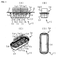
- FIG. 1 illustrates a light emitting device module 1 which constitutes a part of the lighting fixture according to a first embodiment of the present invention.
- FIG. 1(A) is a left side view of the light emitting device module 1, being a partial sectional view
- FIG. 1(B) is a front view of the light emitting device module 1
- FIG. 1(C) is a perspective view from the front, left and lower side
- FIG. 1(D) is a bottom view of the light emitting device module 1.
- the reference numeral 1a indicates a light emitting device such as an LED, for instance.
- the reference numeral 1b indicates a reflector provided with a reflection surface for reflecting the light emitted from the light emitting device 1a downwardly (toward the lower side in FIG. 1 (A) and FIG. 1(B) ).
- the reference numeral 1c indicates a lens mounted on the reflector 1b for controlling a light distribution of the light directly from the light emitting device 1a and the light reflected from the reflection surface of the reflector 1b.
- the reference numeral 1d indicates a thermal interface material for supporting the light emitting device 1a and the reflector 1b, and for radiating or conducting the heat generated by the light emitting device 1a.
- the reference numeral 1e indicates housing for supporting the thermal interface material 1d.
- the reference numeral 1e1 indicates a fin which constitutes a part of the housing 1e.
- the reference numeral 1f indicates a cover for covering the light emitting device 1a, the reflector 1b, the lens 1c, and the thermal interface material 1d.
- the reference numeral 2 indicates an installation member for mounting the light emitting device 1 thereon.
- a part of the heat generated by the light emitting device 1a is radiated from the thermal interface material 1d.
- a part of the heat generated from the light emitting device 1a is thermally conducted to the fin 1e1 of the housing 1e, via the thermal interface material 1d, and the heat is radiated from the fin 1e1.
- a part of the heat generated from the light emitting device 1a is thermally conducted to the installation member 2, via the thermal interface material 1d and the housing 1e, and the heat is radiated from the installation member 2.
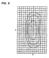
- FIG. 2 illustrates a light distribution pattern, which is emitted from the light emitting device module 1 as shown in FIG. 1 .
- the left side of FIG. 2 corresponds to the rear side (lower-left side of FIG. 1(C) ) of the light emitting device module 1 shown in FIG. 1
- the right side of FIG. 2 corresponds to the front side (upper-right side of FIG. 1(C) ) of the light emitting device module 1 shown in FIG. 1
- the upper side of FIG. 2 corresponds to the right side (lower-right side of FIG. 1(C) ) of the light emitting device module 1 as shown in FIG. 1
- the left side of FIG. 2 corresponds to the left side (upper-left side of FIG. 1 (C) ) of the light emitting device module shown in FIG. 1 .
- a converging property of the lens 1c is configured in such a manner that a degree of light convergence of the light emitting device module 1 in the lateral direction (in the front-rear direction of FIG. 1(A) , lateral direction of FIG. 1(B) , upper left-lower right direction of FIG. 1(C) , lateral direction of FIG. 1 (D) , and upper-lower direction of FIG. 2 ) is made smaller than the degree of light convergence of the light emitting device module 1 in the longitudinal direction (in the lateral direction of FIG. 1(A) , the front-rear direction of FIG. 1(B) , upper right-lower left direction of FIG. 1(C) , upper-lower direction of FIG. 1(D) , and lateral direction of FIG. 2 ).
- the light distribution pattern emitted from the light emitting device module 1 is set as being longer in the lateral direction (upper-lower direction in FIG. 2 ) than in the longitudinal direction (lateral direction in FIG. 2 ).
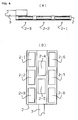
- FIG. 3 and FIG. 4 illustrate the installation member 2, on which multiple light emitting device modules 1, one of which is shown in FIG. 1 , are mounted, and a support 3 for supporting the installation member 2.
- FIG. 3(A) is a plan view of the installation member 2 and a part of the support 3
- FIG. 3(B) is a front view of the installation member 2 and a part of the support 3
- FIG. 4 (A) is a left side view of the installation member 2 and a part of the support 3
- FIG. 4(B) is a bottom view of the installation member 2 and a part of the support 3.
- the installation member 2 is divided into eight partitions, 2-1, 2-2, 2-3, 2-4, 2-5, 2-6, 2-7, and 2-8.
- the partitions 2-1, 2-2, and 2-3, the partitions 2-4 and 2-5, and the partitions 2-6, 2-7, and 2-8 are bent in two stages.
- FIG. 5 to FIG. 7 illustrate the state where eight light emitting device modules 1 (1-1, 1-2, 1-3, 1-4, 1-5, 1-6, 1-7, and 1-8) shown in FIG. 1 are mounted on the installation member 2 as shown in FIG. 3 and FIG. 4 .
- FIG. 5(A) is a plan view of the installation member 2 on which the light emitting device modules 1 (1-1, 1-2, 1-3, 1-4, 1-5, 1-6, 1-7, and 1-8) are mounted and a part of the support 3
- FIG. 5(B) is a front view of the installation member 2 on which the light emitting device modules 1 (1-1, 1-2, 1-3, 1-4, 1-5, 1-6, 1-7, and 1-8) are mounted and a part of the support 3.
- FIG. 6 (A) is a left side view of the installation member 2 on which the light emitting device modules 1 (1-1, 1-2, 1-3, 1-4, 1-5, 1-6, 1-7, and 1-8) are mounted and a part of the support 3
- FIG. 6(B) is a bottom view of the installation member 2 on which the light emitting device modules 1 (1-1, 1-2, 1-3, 1-4, 1-5, 1-6, 1-7, and 1-8) are mounted and a part of the support 3.
- FIG. 7 (A) is a similar illustration of FIG. 5(B) , which illustrates the positional relationship among the light emitting device modules 1-2, 1-4, and 1-7, being mounted on the installation member 2
- FIG. 7(B) is a similar illustration of FIG. 5(B) , which illustrates the positional relationship among the light emitting device modules 1-2, 1-5, and 1-7, being mounted on the installation member 2
- FIG. 7(C) is a similar illustration of FIG. 5(B) , which illustrates the positional relationship among the light emitting device modules 1-3, 1-5, and 1-8, being mounted on the installation member 2.
- FIG. 8 is an overall view of the lighting fixture 10 according to the first embodiment.
- FIG. 8(A) is a front view of the lighting fixture 10 of the first embodiment
- FIG. 8(B) is a left side view of the lighting fixture 10 of the first embodiment.
- the main optical axis lines L1-4 and L1-5 of the light emitting device modules 1-4 and 1-5 being positioned at the center are directed in the 1-ower side.
- the main optical axis lines L1-1, L1-2, and L1-3 of the light emitting devices modules 1-1, 1-2, and 1-3 being positioned at the left side in the figure are pointed to the lower-right direction, and those of the light emitting device modules 1-6, 1-7, and 1-8 being positioned at the right side in the figure are pointed to the lower-left direction.
- the main optical axis lines of the light emitting device modules arranged on the left and right sides are in skew position with respect to the main optical axis lines L1-4 and L1-5 of the light emitting device modules 1-4 and 1-5 placed at the center, being displaced from one another in the longitudinal direction.
- the main optical axis line L1-4 of the light emitting device module 1-4 is in skew position with respect to the main axis lines L1-1, L1-2, L1-6, and L1-7 of the light emitting device modules 1-1, 1-2, 1-6, and 1-7.
- the main optical axis line L1-5 of the light emitting device module 1-5 is in skew position with respect to the main axis lines L1-2, L1-3, L1-7, and L1-8 of the light emitting device modules 1-2, 1-3, 1-7, and 1-8.
- the light emitting device modules at the positions opposed to each other on the both sides are arranged in such a manner that the main optical axis line of one side and the main optical axis line of the other form a certain angle larger than zero degree.
- the angle between the main optical axis line L1-1 of the light emitting device module 1-1 and the main optical axis line L1-6 of the light emitting device module 1-6, the angle between the main optical axis line L1-2 of the light emitting device module 1-2 and the main optical axis line L1-7 of the light emitting device module 1-7, and the angle between the main optical axis line L1-3 of the light emitting device module 1-3 and the main optical axis line L1-8 of the light emitting device module 1-8, are larger than zero degree respectively.
- the eight light emitting device modules 1-1, 1-2, 1-3, 1-4, 1-5, 1-6, 1-7, and 1-8 are allowed to illuminate different directions.
- all the fins 1-1e1 to 1-8e1 are parallel with respect to the vertical plane, and those fins are arranged in such a manner that the roots of the fins are positioned lower than the tips thereof.
- the light emitting device module 1-1 is taken as an example for explanation.
- all the fins 1-1e1 are arranged so that those fins are made parallel with respect to the vertical plane, and the roots of the fins 1-1e1 (the lower-right part of FIG. 5(B) ) are positioned lower than the tips of the fins 1-2e1 (the upper-left part of FIG. 5(B) ).
- the air that received the heat from the fin 1-1e1 of the light emitting device module 1-1 is allowed to rise directly above along the surface of the fin 1-1e1. Consequently, the radiation by the fin 1-1e1 can be enhanced most effectively.
- the situation above is similarly applicable to all the fins 1-1e1 to 1-8e1 of all the light emitting device modules 1-1 to 1-8. Accordingly, while preventing the radiation efficiency by the fins 1-1e1, 1-2e1, 1-3e1, 1-4e1, 1-5e1, 1-6e1, 1-7e1, and 1-8e1, from being deteriorated, the eight light emitting device modules 1-1, 1-2, 1-3, 1-4, 1-5, 1-6, 1-7, and 1-8 are allowed to illuminate different directions.
- the area illuminated by one light emitting device module 1 does not coincide approximately with the area illuminated by the overall lighting fixture, but the area illuminated by one light emitting device module 1 is made smaller than the area illuminated by the overall lighting fixture.
- an illumination area of the overall lighting fixture is divided into multiple small areas, and the illumination area of one light emitting device module 1 is allocated to one of the small areas. There is provided an overlapping part between the illumination areas of adjacent two light emitting device modules.
- the lighting fixture of the second embodiment is different from the first embodiment in the point that a light emitting device module 1 as shown in FIG. 9 is employed instead of the light emitting device module 1 shown in FIG. 1 . Except this point, the lighting fixture of the second embodiment has almost the same configuration as the lighting fixture 10 of the aforementioned first embodiment, and it is able to produce an approximately similar effect.
- FIG. 9 illustrates the light emitting device module 1 constituting a part of the lighting fixture according to the second embodiment.
- FIG. 9(A) is a plan view of the light emitting device module 1 of the lighting fixture of the second embodiment
- FIG. 9(B) is a left side view of the light emitting device module 1 of the lighting fixture of the second embodiment, partially illustrated in section
- FIG. 9(C) is a front view of the light emitting device module 1 of the lighting fixture of the second embodiment, partially illustrated in section
- FIG. 9(D) is a bottom view of the light emitting device module 1 of the lighting fixture of the second embodiment.
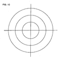
- FIG. 10 illustrates a light distribution pattern of the light emitted from the light emitting device module 1 of the lighting fixture according to the second embodiment as shown in FIG. 9 .
- the lighting fixture 10 of the first embodiment three light emitting devices 1a are provided on the light emitting device module 1 as shown in FIG. 1 , and as shown in FIG. 2 , the light distribution pattern emitted from the light emitting device module 1 is configured in such a manner as being more elongated in the lateral direction (upper-lower direction in FIG. 2 ), than the longitudinal direction (the left-right direction in FIG. 2 ).
- the lighting fixture of the second embodiment instead, as shown in FIG. 9 , one light emitting device 1a having an approximately circular shape is provided on the light emitting device module 1, and as shown in FIG.
- the light distribution pattern of the light emitted from the light emitting device module 1 is configured in such a manner as forming an approximately circular shape having a center located at the main optical axis line L1 (see FIG. 9(B) and FIG. 9(C) ).
- the light distribution pattern of the light emitting device module 1 is formed in an approximately circular shape having a center located at the main optical axis line L1 of the light emitting device module 1, so that a position where the light from the light emitting device module reaches is not changed, even when the light emitting device module is turned around (rotated) with respect to the installation member 2 (see FIG. 3 and FIG. 4 ).
- the main optical axis lines L1-1, L1-2, and L1-3 of the light emitting devices modules 1-1, 1-2, and 1-3 respectively mounted on the partitions 2-1, 2-2, and 2-3 of the installation member 2 are pointed to the lower right direction
- the main optical axis lines L1-6, L1-7, and L1-8 of the light emitting devices modules 1-6, 1-7, and 1-8 respectively mounted on the partitions 2-6, 2-7, and 2-8 of the installation member 2 are pointed to the lower left direction.
- the main optical axis lines L1-1, L1-2, and L1-3 of the light emitting devices modules 1-1, 1-2, and 1-3 respectively mounted on the partitions 2-1, 2-2, and 2-3 of the installation member 2 may be pointed to the lower right direction and also pointed to the front
- the main optical axis lines L1-6, L1-7, and L1-8 of the light emitting devices modules 1-6, 1-7, and 1-8 respectively mounted on the partitions 2-6, 2-7, and 2-8 of the installation member 2 may be pointed to the lower left direction and also pointed to the front.
- the lighting fixture of a third embodiment when the light emitting device module 1 (see FIG. 9 ) is turned around to be mounted on the installation member 2 (see FIG. 3 and FIG. 4 ), the air that received the heat from the fins 1e1 of all the light emitting device module 1 is allowed to rise directly above along the surface of the fins 1e1, similar to the lighting fixture of the first and the second embodiments.
- the light emitting device module 1 when the light emitting device module 1 (see FIG. 9 ) is turned around to be mounted on the installation member 2 (see FIG. 3 and FIG.
- all the fins 1e1 become in parallel with respect to the vertical plane, and can be arranged in such manner that the roots of the fins 1e1 is positioned lower than the tips of the fins 1e1. Consequently, also the lighting fixture of the third embodiment is able to enhance the heat radiation by the fins 1e1 most effectively, similar to the lighting fixture of the first and that of the second embodiment.
- the lighting fixture of the fourth embodiment has almost the same configuration and produces almost the same effect as the aforementioned lighting fixture 10 of the first embodiment, except a point that a light emitting device module 1 as shown in FIG. 11 is employed.
- FIG. 11 illustrates the light emitting device module 1 constituting a part of the lighting fixture of the fourth embodiment.
- FIG. 11 (A) is a plan view of the light emitting device module 1 of the lighting fixture of the fourth embodiment
- FIG. 11(B) is a left side view of the light emitting device module 1 of the lighting fixture of the fourth embodiment, partially illustrated in section
- FIG. 11(C) is a front view of the light emitting device module 1 of the lighting fixture of the fourth embodiment, partially illustrated in section
- FIG. 11(D) is a bottom view of the light emitting device module 1 of the lighting fixture of the fourth embodiment.
- the light distribution pattern emitted from the light emitting device module 1 is configured in such a manner as forming an approximately circular shape having a center located at the main optical axis line L1 of the light emitting device module 1 (see FIG. 11(B) and FIG. 11(C) ).
- the lighting fixture 10 of the first embodiment as shown in FIG. 1 , three sets made up of the light emitting device 1a, the reflector 1b, the lens 1c, and the thermal interface material 1d are linearly arranged.
- the lighting fixture of the fourth embodiment as shown in FIG.
- a set made up of the light emitting device 1a1, the reflector 1b1, the lens 1c1, and the thermal interface material 1d1 a set made up of the light emitting device 1a2, the reflector 1b2, the lens 1c2, and the thermal interface 1d2, a set made up of the light emitting device 1a3, the reflector 1b3, the lens 1c3, and the thermal interface material 1d3, and a set made up of the light emitting device 1a4, the reflector 1b4, the lens 1c4, and the thermal interface material 1d4 are arranged on the circle.
- the light-distribution pattern of the light emitting device module is formed in an approximately circular shape having a center located at the main optical axis line L1 of the light emitting device module, so that a position where the light emitted from the light emitting device module 1 reaches is not changed, even when the light emitting device module 1 is turned around on the installation member 2 (see FIG. 3 and FIG. 4 ).
- the main optical axis lines L1-1, L1-2, and L1-3 of the light emitting device modules 1-1, 1-2, and 1-3 respectively mounted on the partitions 2-1, 2-2, and 2-3 of the installation member 2 are pointed to the lower right direction
- the main optical axis lines L1-6, L1-7, and L1-8 of the light emitting device modules 1-6, 1-7, and 1-8 respectively mounted on the partitions 2-6, 2-7, and 2-8 of the installation member 2 are pointed to the lower left direction.
- the main optical axis lines L1-1 L1-2, and L1-3 of the light emitting device modules 1-1, 1-2, and 1-3 respectively mounted on the partitions 2-1, 2-2, and 2-3 of the installation member 2 may be pointed to the lower right direction and also pointed to the front
- the main optical axis lines L1-6, L1-7, and L1-8 of the light emitting device modules 1-6, 1-7, and 1-8 respectively mounted on the partitions 2-6, 2-7, and 2-8 of the installation member 2 may be pointed to the lower left direction and also pointed to the front.
- the air that received the heat from all the fins 1e1 of the light emitting device module 1 is allowed to rise directly above along the surface of each fin 1e1, similar to the lighting fixture of the first embodiment and that of the fourth embodiment.
- the light emitting device module 1 when the light emitting device module 1 (see FIG. 11 ) is turned around to be mounted on the installation member 2 (see FIG. 3 and FIG. 4 ), all the fins 1e1 become parallel with respect to the vertical plane, and all the fins 1e1 can be arranged in such a manner that the roots of the fins 1e1 are positioned lower than the tips of the fins 1e1. Consequently, also according to the lighting fixture of the fifth embodiment, the radiation by the fins 1e1 can be enhanced most efficiently.
- each light emitting device 1a1, 1a2, 1a3, and 1a4 are arranged on the circle having as the center thereof, the main optical axis line L1 of the light emitting device module 1.
- an arbitrary number of light emitting devices, at least two, are arranged on the circle having a center located at the main optical axis line L1 of the light emitting device, and the light distribution pattern emitted from the light emitting device module 1 may form an approximately circular shape having a center located at the main optical axis line L1 of the light emitting device module 1.
- the installation member 2 is directly mounted on the support 3.
- the installation member 2 may be indirectly mounted on the support 3.
- the thermal interface material (heat transfer member) 1d has a heat radiating function, in addition to the heat transferring function.
- FIG. 12 is an enlarged sectional view of the thermal interface material (heat transfer member) 1d (see FIG. 1 ) of the lighting fixture according to the eighth embodiment.
- a covering layer is not formed on a part exposed to the air, on the surface of the thermal interface material (heat transfer member) 1d having a function of heat radiation.
- the covering layer is formed at the part 1d4 exposed to the air, on the surface of the thermal interface material (heat transfer member) 1d having the function of heat radiation. Consequently, the efficiency for cooling the light emitting device 1a by the thermal interface material (heat transfer member) 1d is enhanced.
- the part 1d4 exposed to the air on the surface of the thermal interface material (heat transfer member) 1d may be subjected to a roughening process (the ninth embodiment).
- the covering layer is not formed at the part that is in contact with a thing other than the air, on the surface of the thermal interface material (heat transfer member) 1d having the function of heat transfer.
- the covering layer is not formed, at the part 1d1 being in contact with the light emitting device, at the part 1d2 being in contact with the reflector 1b, and at the part 1d3 that is in contact wit the housing 1e.
- the part where the covering layer is not formed on the surface of the thermal interface material (heat transfer member) 1d having the heat transfer function that is, the part 1d1 being in contact with the light emitting device 1a, the part 1d2 being in contact with the reflector 1b, the part 1d3 being in contact with the housing 1e, are all polished. Consequently, the heat transfer resistance is reduced between the thermal interface material (heat transfer member) 1d, and those elements; the light emitting device 1a, the reflector 1b, and the housing 1e.
- these parts 1d1, 1d2, and 1d3 may be left as solid surfaces, instead of being polished (the tenth embodiment).
- FIG. 13 is an enlarged sectional view of the housing 1e (see FIG. 1 ) of the lighting fixture of the eighth embodiment.
- a covering layer is not formed at a part of the fin 1e1 exposed to the air, nor at a part exposed to the air other than the fin 1e1.
- the covering layer is formed at the part of the fin 1e1 exposed to the air, and the part exposed to the air other than the fin 1e1, on the surface of the housing 1e having the heat radiation function. Consequently, efficiency for cooling the light emitting device 1a by the housing 1e is enhanced.
- the covering layer is not formed at the part being in contact with the thing other than the air, on the surface of the housing 1e having the heat transfer function.
- the covering layers on the surface of the housing 1e, there are not formed the covering layers at the part 1e2 being in contact with the thermal interface material (heat transfer member) 1d, and at the part 1e3 being in contact with the installation member 2.
- the parts on which the covering layer is not formed are polished. Consequently, the heat transfer resistance is reduced between the housing 1e and the following elements; the heat transfer member 1d and the installation member 2.
- the part 1e2 being in contact with the thermal interface material (heat transfer member) 1d, and the part 1e3 being in contact with the installation member 2 may be left as solid surfaces, instead of being polished (the twelfth embodiment).
- FIG. 14 is a sectional view of a part of the installation member 2 (see FIG. 1 ) of the lighting fixture of the eighth embodiment.
- a covering layer is not formed at the part exposed to the air on the surface of the installation member 2 having the heat radiation function.
- the covering layer is formed at the part 2b exposed to the air on the surface of the installation member 2 having the heat radiation function. Consequently, the efficiency for cooling the light emitting device 1a by the installation member 2 is enhanced.
- the part 2b exposed to the air on the surface of the installation member 2 may be subjected to the roughening process, instead of forming the covering layer thereon (the thirteenth embodiment).
- a covering layer is not formed on a part being in contact with the thing other than the air, on the surface of the installation member 2 having the heat transfer function.
- the covering layer is not formed at the part 2a being in contact with the housing 1e, on the surface of the installation member 2. This part is polished. Consequently, the heat transfer resistance between the installation member 2 and the housing 1e is reduced.
- part 2a being in contact with the housing 1e, on the surface of the installation member 2 may be left as a solid surface, instead of being polished (the fourteenth embodiment).
- a grease-like or a sheet-like thermally conductive interface material may be placed between the members directly contacting.
- the light emitting device 1a directly contacts the part 1d1 on the surface of the thermal interface material (heat transfer member) 1d, and the above thermally conductive interface material may be placed therebetween (the fifteenth embodiment).
- the thermal interface material (heat transfer member) 1d comes into contact with the reflector 1b directly at the part 1d2, and the thermally conductive interface material may be placed therebetween (the sixteenth embodiment).
- the part 1d3 being in contact with the housing 1e on the surface of the thermal interface material (heat transfer member) 1d directly contacts the part 1e2 that comes into contact with the heat transfer member 1d on the surface of the housing 1e.
- the thermally conductive interface material may be placed therebetween (the seventeenth embodiment).
- the part 1e3 being in contact with the installation member 2 on the surface of the housing 1e directly contacts the part 2a that comes into contact with the housing 1e on the surface of the installation member 2.
- the thermally conductive interface material may be placed therebetween (the eighteenth embodiment).
- three sets of the light emitting device 1a, the reflector 1b, and the lens 1c are provided on one light emitting device module 1.
- an arbitrary number of sets of the light emitting device 1a, the reflector 1b, and the lens 1c, other than three, may be provided on one light emitting device module 1 (the nineteenth embodiment).
- a covering layer is not formed on a part being in contact with a lampshade (not illustrated) on the surface of the installation member 2 having the heat transferring function.
- This part is polished, for example. Consequently, the heat transfer resistance between the installation member 2 and the lampshade is reduced.
- the part being in contact with the lampshade on the surface of the installation member 2 may be left as a solid surface, instead of being polished (the twentieth embodiment).
- the covering layer is formed at the part exposed to the air on the surface of the lampshade (not illustrated) having the heat radiation function. Consequently, efficiency for cooling the light emitting device 1 by the lampshade (not illustrated) is enhanced.
- a roughening process may be performed thereon (the twenty-first embodiment).
- the covering layer is not formed at the part contacting a thing other than the air on the surface of the lampshade having the heat transferring function, specifically, the part contacting the installation member 2. This part is polished. Consequently, the heat transfer resistance between the lampshade and the installation member 2 is reduced.
- the part of the lampshade, contacting the installation member 2 may be left as a solid surface, instead of being polished (the twenty-second embodiment).
- the part contacting the lampshade (not illustrated), on the surface of the installation member 2 directly contacts the part that is in contact with the installation member 2 on the surface of the lampshade.
- a grease-like or a sheet-like thermally conductive interface material may be placed therebetween (the twenty-third embodiment).
- a covering layer is not formed on the part that is in contact with the support 3. This part is polished preferably. Consequently, the heat transfer resistance between the installation member 2 and the support 3 is reduced.
- the part of the installation member 2, which is in contact with the support 3, may be left as a solid surface, instead of being polished (the twenty-fourth embodiment).
- the covering layer is not formed at the part exposed to the air on the surface of the support 3 having the heat radiation function.
- the covering layer is formed at the part exposed to the air on the surface of the support 3 having the heat radiation function. Consequently, the efficiency for cooling the light emitting device 1a by the support 3 is enhanced.
- the part exposed to the air may be subjected to the roughening process, instead of forming the covering layer thereon (the twenty-fifth embodiment).
- the covering layer is not formed at the part being in contact with the thing other than the air, specifically, at the part being in contact with the installation member 2.
- the part is polished, preferably. Consequently, the heat transfer resistance between the support 3 and the installation member 2 is reduced.
- the part contacting the installation member 2 may be left as a solid surface instead of being polished (the twenty-sixth embodiment).
- the part being in contact with the support 3 directly contacts the part that is in contact with the installation member 2 on the surface of the support 3.
- a grease-like or a sheet-like thermally conductive interface material may be placed therebetween (the twenty-seventh embodiment).
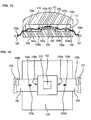
- FIG. 15 is a sectional view of a primary portion of the light emitting device module of the lighting fixture according to the twenty-eighth embodiment.
- FIG. 16 is a plan view of the primary portion of the light emitting device module of the lighting fixture according to the twenty-eighth embodiment in the state where the lens 110 is removed.
- FIG. 16 is an illustration of the primary portion of the light emitting device module of the lighting fixture of the twenty-eighth embodiment, when viewing FIG. 15 from the top, in the state where the lens 110 is removed.
- the lighting fixture of the twenty-eighth embodiment is configured as approximately the same as the lighting fixture 10 of the aforementioned first embodiment, except some points described below. Therefore, according to the lighting fixture of the twenty-eighth embodiment, it is possible to produce approximately the same effect of the lighting fixture 10 of the aforementioned first embodiment.
- the primary portion of the light emitting device module 1 is made up of the light emitting device 1a, the reflector 1b, the lens 1c, and the thermal interface material 1d.
- the primary portion of the light emitting device module is configured as shown in FIG. 15 and FIG. 16 .
- the reference numeral 101 indicates a light emitting device like an LED chip, for example, and the reference numeral 102 indicates a fluorescence substance applied on the light emitting device 101.
- the reference numeral 103 indicates a base for supporting the light emitting device 101 and the fluorescence substance 102.
- the reference numerals 103a and 103b indicate light-emitting device feeding electrodes formed on the lower surface of the base 103, for feeding the light emitting device 101, which is placed on the base 103.
- the light emitting device 101, the fluorescence substance 10.2, and the base 103 constitute a package like an LED package, for example.
- the light emitting device feeding electrode 103a is electrically connected to an anode electrode (not illustrated), and the light emitting device feeding electrode 103b is electrically connected to a cathode electrode (not illustrated) of the light emitting device 101.
- the base 103 is made of a material having a relatively high thermal conductivity.
- the reference numeral 104 indicates a substrate for supporting the base 103
- the reference numeral 105 indicates an adhesive agent for fixing the base 103 onto the substrate 104.
- the substrate 104 is made of a material having a relatively high thermal conductivity, such as Al and ADC (Aluminum Die-Cast), and the adhesive agent is made of a material having a relatively high thermal conductivity.
- the reference numerals 106 and 107 indicate external electrodes for feeding the light emitting device 101.
- the external electrodes 106 and 107 are configured in such a manner as movable with respect to the light emitting device 101. Alternatively, these electrodes are placed at the positions relatively distant from the light emitting device 101 to such an extent that the temperature of the external electrodes 106 and 107 is not raised even when that light emitting device 101 generates heat.
- the reference numeral 108 indicates a flexible substrate as a connecting member for connecting the light emitting device feeding electrode 103a and the external electrode 106.
- the reference numerals 108a and 108b indicate terminals formed on the flexible substrate 108
- the reference numeral 108c indicates an elongate hole for guiding via the terminal 108a, the flexible substrate 108 connected to the light emitting device feeding electrode 103a of the base 103 toward the external electrode 106 side.
- the reference numeral 104c indicates a protrusion placed on the upper surface of the substrate 104, for fitting into the elongate hole 108c slidably.
- the flexible substrate 108 is connected to the external electrode 106 via the terminal 108b.
- the terminal 108a of the flexible substrate 108 is connected to the light emitting device feeding electrode 103a by soldering (not illustrated), and the terminal 108b of the flexible substrate 108 is connected to the external electrode 106 by soldering (not illustrated).
- the terminal 108a of the flexible substrate 108 may be connected to the light emitting device feeding electrode 103a via a connector (not illustrated), and the terminal 108b of the flexible substrate 108 may be connected to the external electrode 106 via a connector (not illustrated) (the twenty-ninth embodiment).
- the reference numeral 109 indicates a flexible substrate as a connecting member for connecting the light emitting device feeding electrode 103b with the external electrode 107.
- the reference numeral 109a and 109b indicate the terminals formed on the flexible substrate 109, and the reference numeral 109c indicates an elongate hole for guiding via the terminal 109a, the flexible substrate 109 connected to the light emitting device feeding electrode 103b of the base 103 toward the external electrode 107 side.
- the reference numeral 104d indicates a protrusion placed on the upper surface of the substrate 104, for fitting into the elongate hole 109c slidably.
- the flexible substrate 109 is connected to the external electrode 107 via the terminal 109b.
- the terminal 109a of the flexible substrate 109 is connected to the light emitting device feeding electrode 103b by soldering (not illustrated)
- the terminal 109b of the flexible substrate 109 is connected to the external electrode 107 by soldering (not illustrate).
- the terminal 109a of the flexible substrate 109 may be connected to the light emitting device feeding electrode 103b via a connector (not illustrated)
- the terminal 109b of the flexible substrate 109 may be connected to the external electrode 107 via a connector (not illustrated) (the thirtieth embodiment).
- the reference numeral 111 indicates a space between the upper surface of the fluorescence substance 102, the base 103, and the substrate 104, and the lower surface of the lens 110.
- the reference numeral 104a indicates a gutter, serving as an anti-running means for preventing the adhesive agent 105 from flowing out from between the base 103 and the substrate 104 toward the side of the external electrode 106 (the left side of FIG. 15 ).
- the reference numeral 104b indicates a gutter, serving as an anti-running means for preventing the adhesive agent 105 from flowing out from between the base 103 and the substrate 104 toward the side of the external electrode 107 (the right side of FIG. 15 ).
- FIG. 17 is an enlarged illustration of the gutters 104a and 104b shown in FIG. 15 .
- the gutter 104a is provided so that even though the adhesive agent 105 flows out from between the base 103 and the substrate 104 toward the side of the external electrode 106 (the left side of FIG. 15 and FIG. 17 ), the adhesive agent 105 flown out is stopped by the gutter 104a and prevented from reaching the light emitting device feeding electrode 103a and the terminal 108a.
- the gutter 104b is provided so that even though the adhesive agent 105 flows out from between the base 103 and the substrate 104 toward the side of the external electrode 107 (the right side of FIG. 15 and FIG. 17 ), the adhesive agent 105 flown out is stopped by the gutter 104b and prevented from reaching the light emitting device feeding electrode 103b and the terminal 109a.
- the flexible substrate 108 connecting the light emitting device feeding electrode 103a and the external electrode 106, and the flexible substrate 109 connecting the light emitting device feeding electrode 103b and the external electrode 107 are placed within the space 111, not sealed by resin.
- This configuration enables to reduce a thermal stress applied on the flexible substrates 108 and 109 more than the case where the flexible substrates 108 and 109 are sealed by resin.
- the external electrode 106 is configured as movable with respect to the light emitting device 101, or, the electrode is placed at the position relatively distant from the light emitting device 101 to such an extent that the temperature of the external electrodes 106 is not raised even when that light emitting device 101 generates heat.
- the flexible substrate 108 is constrained so that out of the two terminals 108a and 108b of the flexible substrate 108, the terminal 108a connected to the light emitting device feeding electrode 103a serves as a fixed end, and the terminal 108b connected to the external electrode 106 serves as a free end. That is, the flexible substrate 108 is constrained in such a manner as substantially forming the cantilever structure.
- the thermal stress applied to the flexible substrate 108 more than the case where both the terminal 108a connected to the light emitting device feeding electrode 103a and the terminal 108b connected to the external electrode 106 are configured as fixed ends, i.e., the flexible substrate 108 is constrained to substantially form a fixed beam structure.
- the thermal stress applied to the flexible substrate 108 can be reduced.
- the lighting fixture of the twenty-eighth embodiment is configured in such a manner that only the terminal 108a of the flexible substrate 108 is constrained, and the other part is not constrained. Therefore, even when the temperature of the flexible substrate 108 is raised along with the heat generation by the light emitting device 101, the flexible substrate 108 is allowed to be thermally expanded freely, without applying the thermal stress to the flexible substrate 108. In other words, by reducing the thermal stress applied to the flexible substrate 108, the possibility of solder separation may be reduced, and thereby the reliability can be enhanced.
- the light emitting device feeding electrode 103a is connected to the external electrode 106 via the flexible substrate 108.
- the light emitting device feeding electrode 103a may be connected to the external electrode 106 by any connecting member, such as a wire and a glass epoxy substrate, for instance (the thirty-first embodiment).
- the external electrode 106 is configured in such a manner as movable with respect to the light emitting device 101.
- the external electrode 106 is arranged at a position relatively distant from the light emitting device 101 to such an extent that the temperature of the external electrodes 106 is not raised even when that light emitting device 101 generates heat.
- the connecting member is constrained in such a manner that one terminal connected to the light emitting device feeding electrode 103a, out of the two terminals of the connecting member, serves a fixed end, and another terminal connected to the external electrode 106 serves as a free end. That is, the connecting member is constrained in such a manner as substantially forming the cantilever structure. Therefore, also according to the lighting fixture of the thirty-first embodiment, an effect approximately the same as the effect of the twenty-eighth embodiment can be produced.
- the flexible substrate 109 that connects the light emitting device 101 and the external electrode 107 has exactly the same configuration as the flexible substrate 108, and the flexible substrate 109 is constrained in such a manner as substantially forming the cantilever structure. Therefore, even when the temperature of the flexible substrate 109 is raised along with the heat generation by the light emitting device 101, the flexible substrate 109 is allowed to be thermally expanded freely, without applying the thermal stress thereto, and the possibility of solder separation may be reduced, thereby enhancing the reliability.
- the light emitting device feeding electrode 103b may be connected to the external electrode 107 by any connecting member, such as a wire and a glass epoxy substrate, for instance (the thirsty-second embodiment), and the same effect can be obtained.
- the substrate 104 that is the heat radiation member for radiating the heat generated by the light emitting device 101 is arranged at a position closer to the light emitting device 101 than the light-emitting feeding electrodes 103a and 103b.
- the heat generated by the light emitting device 101 is thermally conducted to the substrate 104 via the base 103 and the adhesive agent 105, and radiated from the lower surface of the substrate 104.
- the thermal stress applied to the flexible substrates 108 and 109 more than the case where the substrate 104 as the heat radiation member for radiating the heat generated by the light emitting device 101 is arranged at a position more distant from the light emitting device 101 than the light emitting device feeding electrode 103a and 103b.
- the lighting fixture of the thirty-third embodiment has almost the same configuration as the lighting fixture of the aforementioned twenty-eighth embodiment, except the points described below. Therefore, the lighting fixture of the thirty-third embodiment can produce almost the same effect as the lighting fixture of the aforementioned twenty-eighth embodiment, except the points described below.
- FIG. 18 is a sectional view of a primary portion of the light emitting device module of the lighting fixture according to the thirty-third embodiment.
- FIG. 19 is a plan view of the light emitting device module of the lighting fixture according to the thirty-third embodiment in the state where the lens 110 is removed.
- FIG. 19 is an illustration of the primary portion of the light emitting device module of the lighting fixture according to the thirty-third embodiment, when viewing FIG. 18 from the top, in the state where the lens 110 is removed.
- the light emitting device feeding electrodes 103a and 103b are formed on the lower surface of the base 103.
- the light emitting device feeding electrodes 103a and 103b are formed on the upper surface of the base 103.
- the substrate 104 is formed in a convex shape.
- the substrate 104 is formed in a concave shape.
- the substrate 104 is configured in such a manner that the base 103 is positioned in the concave part 104e of the substrate 104.
- the external electrodes 106 and 107 are configured in such a manner as movable with respect to the light emitting device 101.
- the external electrodes 106 and 107 are arranged at the positions relatively distant from the light emitting device 101 to such an extent that the temperature of the external electrodes 106 and 107 is not raised, even when the light emitting device 101 generates heat.
- the terminals 108a and 108b of the flexible substrate 108 are respectively connected to the light emitting device feeding electrodes 103a and the external electrode 106 by soldering (not illustrated).
- the terminal 108a of the flexible substrate 108 may be connected to the light emitting device feeding electrode 103a via the connector (not illustrated), and the terminal 108b of the flexible substrate 108 may be connected to the external electrode 106 via the connector (not illustrated) (the thirty-fourth embodiment).
- connection of the terminals 109a and 109b of the flexible substrate 109, respectively with the light emitting device feeding electrode 103b and the external electrode 107, may be made by the connector, instead of the solder (the thirty-fifth embodiment).
- the concave part 104 of the substrate 104 prevents the adhesive agent 105 from flowing out from between the base 103 and the substrate 104 toward the external electrode 106 side (the left side of FIG. 18 and FIG. 19 ), or toward the external electrode 107 sid.e (the right side of FIG. 18 and FIG. 19 ).
- the concave part 104e of the substrate 104 is formed so that the adhesive agent 105 reaches neither the light emitting device feeding electrodes 103a and 103b nor the terminals 108a and 109a on the upper surface of the base 103.
- connection between the light emitting device feeding electrode 103a and the external electrode 106, and the connection between the light emitting device feeding electrode 103b and the external electrode 107 are made by using the flexible substrate 108 and the flexible substrate 109, respectively.
- any connection member such as a wire and a glass epoxy substrate, may be employed (the thirty-sixth embodiment and the thirty-seventh embodiment).
- the substrate 104 serving as the heat radiation member for radiating the heat generated by the light emitting device 101 is arranged at a position closer to the light emitting device 101, than the light emitting device feeding electrodes 103a and 103b.
- the heat generated by the light emitting device 101 is thermally conducted to the substrate 104 via the base 103 and the adhesive agent 105, and radiated from the lower surface of the substrate 104.
- the thermal stress applied to the flexible substrates 108 and 109 more than the case where the substrate 104 serving as the heat radiation member for radiating the heat generated by the light emitting device 101 is arranged at a position distant from the light emitting device 101, than the light emitting device feeding electrodes 103a and 103b.
- the lighting fixture according to the present invention may be applicable to a road lighting, a street light, an indoor lighting, and the like.
Landscapes
- Engineering & Computer Science (AREA)
- General Engineering & Computer Science (AREA)
- Physics & Mathematics (AREA)
- Geometry (AREA)
- Arrangement Of Elements, Cooling, Sealing, Or The Like Of Lighting Devices (AREA)
- Non-Portable Lighting Devices Or Systems Thereof (AREA)
- Led Device Packages (AREA)
Abstract
Description
- The present invention relates to a lighting fixture in which multiple light emitting device modules are provided, each having fins for radiating heat generated by a light emitting device.
- A lighting fixture described in
patent document 1, for example, is equipped with multiple light emitting device modules (LED light-source modules) each having fins for radiating heat generated by a light emitting device (LED). - In this lighting fixture, the light emitting device (LED) is placed on the same surface as the surface where the fins are placed, among all the surfaces of a bridging part (base) for bridging roots of adjacent fins, and a housing of the lighting fixture is made to abut against the surface opposite to the surface where the fins are arranged. As a result, the heat generated from the light emitting device (LED) is radiated from the fins via the bridging part (base), and the heat is also conducted to the housing of the lighting fixture via the bridging part (base).
- In the lighting fixture described in
FIG. 9 of thepatent document 1, multiple light emitting device modules (LED light source modules) are provided, and those multiple light emitting device modules are arranged in such a manner that a main optical axis line of one light emitting device module is parallel to the main optical axis of other light emitting device modules. Therefore, the light from the multiple light emitting device modules cannot illuminate multiple different directions. - If the direction of the main optical axis line of the multiple light emitting device modules is changed in order to make the multiple light emitting device modules illuminate multiple different directions, however, an ascending air current which received the heat from the fins may be obstructed, and thereby an efficiency of the heat radiation by the fins may be deteriorated.
-
- [Patent Document 1]
Japanese Published Unexamined Patent Application No.2004-55229 - In view of the problem above, the present invention is to provide a lighting fixture which allows illumination from the light emitting device modules at wide angle in multiple different directions, while avoiding the deterioration of efficiency of the heat radiation by the fins.
- According to the present invention, a lighting fixture provided with multiple light emitting device modules each including a light emitting device and fins for radiating heat generated by the light emitting device, wherein, all the multiple light emitting device modules are arranged in such a manner that a main optical axis line of one light emitting device module and a main optical axis line of other light emitting device module forms an angle of larger than zero degree, or those main optical axis lines are in skew position, and all the fins are arranged in such a manner that all the fins are parallel with respect to a vertical plane and roots of the fins are located at the same height as or lower than tips of the fins.
- The inventors of the present invention zealously studied at what part a covering layer is to be formed on a surface of a heat radiation member for radiating the heat generated by the light emitting device, in order to enhance efficiency at a maximum in cooling the light emitting device by the heat radiation member.
- As a result of the studies, the present inventors have found the followings: when the covering layer is formed on a part exposed to the air on the surface of the heat radiation member, the efficiency of the heat radiation from the heat radiation member toward the air can be improved, resulting in that the efficiency for cooling the light emitting device by the heat radiation member can be enhanced. However, when the covering layer is formed on a part being in contact with the light emitting device on the surface of the heat radiation member, heat transfer resistance between the light emitting device and the heat radiation member is increased, resulting in that the efficiency for cooling the light emitting device by the heat radiation member is deteriorated.
- In brief, the present inventors have found that the efficiency for cooling the light emitting device by the heat radiation member is more enhanced, when the covering layer is not formed at the part which is in contact with the light emitting device on the surface of the heat radiation member.
- In addition, the present inventors have found that if polishing is performed at a part which comes into contact with the light emitting device on the surface of the heat radiation member, rather than leaving the part as a solid surface, the heat transfer resistance can be reduced, resulting in that the efficiency for cooling the light emitting device by the heat radiation member is more enhanced.
- In particular, the present inventors have found that if a grease-like or a sheet-like thermally conductive interface material is placed on the part which comes into contact with the light emitting device on the surface of the heat radiation member, rather than leaving the part as a solid surface, the heat transfer resistance can be reduced, resulting in that the efficiency for cooling the light emitting device by the heat radiation member is more enhanced.
- Furthermore, the present inventors zealously studied the cooling efficiency of the light emitting device, not only in the case where the light emitting device is directly connected with the heat radiation member but also in the case where the light emitting device is connected with the heat radiation member via the heat transfer member.
- As a result of the study, the present inventors have found that when a covering layer is formed at a part which is exposed to the air on the surface of the heat transfer member, the heat radiation efficiency from the heat transfer member into the air can be enhanced, resulting in that the efficiency for cooling the light emitting device by the heat transfer member may be improved. That is, the heat transfer member is found to function as the heat radiation member.
- In addition, as a result of the study, the present inventors have found that if the covering layer is formed on a part which is in contact with the light emitting device and on a part which is in contact with the heat radiation member, on the surface of the heat transfer member, the heat transfer resistance is increased, resulting in that the efficiency for cooling the light emitting device is deteriorated.
- In other words, the present inventors have found that it is better not to form the covering layer at the part being in contact with the light emitting device and at the part being in contact with the heat radiation member, on the surface of the heat transfer member, in order to enhance the efficiency for cooling the light emitting device.
- In addition, the present inventors have found that if polishing is performed at the part being in contact with the light emitting device and the part being in contact with the heat radiation member, on the surface of the heat transfer member, rather than leaving the parts as solid surfaces, the heat transfer resistance can be reduced, resulting in that the efficiency for cooling the light emitting device by the heat radiation member is more enhanced.
- Furthermore, the present inventors have found that if the thermally conductive interface material is placed at the part being in contact with the light emitting device and at the part being in contact with the heat radiation member, on the surface of the heat transfer member, rather than leaving the parts as solid surfaces, the heat transfer resistance can be reduced, resulting in that the efficiency for cooling the light emitting device by the heat radiation member is more enhanced.
- In addition, based on the same concept as described above, the present inventors zealously studied which part is to be subjected to a roughening process on the surface of the heat radiation member for radiating the heat generated by the light emitting device, in order to enhance the efficiency at a maximum, in cooling the light emitting device by the heat radiation member.
- As a result of the studies, the present inventors have found the followings: when the roughening process is performed at the part exposed to the air on the surface of the heat radiation member, the efficiency of the heat radiation from the heat radiation member towards the air can be improved, resulting in that the efficiency for cooling the light emitting device by the heat radiation member can be enhanced. However, when the roughening process is performed at the part being in contact with to the light emitting device on the surface of the heat radiation member, a heat transfer resistance between the light emitting device and the heat radiation member is increased, resulting in that the efficiency for cooling the light emitting device by the heat radiation member is deteriorated.
- In brief, the present inventors have found that it is better not to perform the roughening process at the part being in contact with the light emitting device on the surface of the heat radiation member, in order to enhance the efficiency for cooling the light emitting device by the heat radiation member.
- In the lighting fixture according to the present invention, multiple light emitting device modules are arranged in such a manner that a main optical axis line of one light emitting device module and a main optical axis line of other light emitting device module form an angle of larger than zero degree, or those main optical axis lines are in skew position. Therefore, the multiple light emitting device modules are allowed to illuminate multiple different directions.
- There are following problems: when the fins are placed at an angle larger than zero degree with respect to the vertical plane, an ascending air current in the lower side of the fins, which received heat from the fins, is obstructed by the fins, and an efficiency of heat radiation by the fins may be deteriorated (problem 1). When the fins are arranged in such a manner that the roots of fins are located at higher lever than the tips of the fins, the bridging part for bridging the roots of adjacent fins may obstruct the ascending air current that received the heat from the fins, resulting in that the heat radiation efficiency by the fins may be deteriorated (problem 2).
- In the lighting fixture according to the present invention, all the fins are arranged in such a manner the all the fins are parallel with respect to the vertical plane, and the roots of the fins are located at the same height as or lower level than the tips of the fins. Therefore, the
above problems - In brief, the lighting fixture of the present invention allows the multiple light emitting device modules to illuminate the multiple different directions, while avoiding deterioration of radiation efficiency by the fins.
- In order that the fins become parallel with respect to the vertical plane, and the roots of the fins are positioned at the same height as or at the lower level than the tips of the fins, the light emitting device modules may have to be turned around (rotated) for installation occasionally.
- However, in a case that a light distribution pattern of the light emitting device module is formed in a polygonal shape, if the light emitting device module is rotated, there is a possibility that a position where the light from the light emitting device module reaches is displaced from a target position, when (problem 3).
- In order to solve the
problem 3, in the lighting fixture of the present invention, preferably, the light-distribution pattern of the light emitting device module is formed in approximately circular shape whose center is located at the main optical axis line of the light emitting device module. - In the lighting fixture of the present invention, one light emitting device of approximately circular shape is provided in each of the light emitting device module. Alternatively, in the lighting fixture of the present invention, preferably, at least two light emitting devices are arranged on the circle whose center is located at the main optical line axis of the light emitting device module.
- Specifically, in the lighting fixture of the present invention, preferably, the light-distribution pattern of the light emitting device module is formed in an approximately circular shape whose center located at the main optical axis line of the light emitting device module, so that a position where the light from the light emitting device module reaches is not changed, even when the light emitting device module is turned around. Accordingly, it is possible to reduce the possibility that the position where the light from the light emitting device module is displaced from the target position, along with rotation of the light emitting device module.
- In the lighting fixture of the present invention, preferably, a covering layer is formed on a part exposed to the air on the surface of the heat radiation member for radiating the heat generated by the light emitting device. Therefore, according to the lighting fixture of the present invention, it is possible to enhance the heat radiation efficiency from the part exposed to the air on the surface of the heat radiation member into the air, whereby the efficiency for cooling the light emitting device by the heat radiation member can be enhanced.
- In the lighting fixture of the present invention, preferably, the covering layer is not formed on a part that is in contact with a thing other than the air, on the surface of the heat radiation member for radiating the heat generated by the light emitting device. Therefore, it is possible to avoid the deterioration of the efficiency for cooling the light emitting device by the heat radiation member, the deterioration being caused by the increase of heat transfer resistance between the thing other than the air and the heat radiation member, if the covering layer is formed at the part being in contact with the thing other than the air on the surface of the heat radiation member. According to the lighting fixture of the present invention, the heat transfer resistance between the thing other than the air and the heat radiation member can be reduced more, than the case where the covering layer is formed at the part being in contact with the thing other than the air on the surface of the heat radiation member. Therefore, it is possible to enhance the efficiency for cooling the light emitting device by the heat radiation member.
- According to the lighting fixture of the present invention, it is possible to reduce the heat transfer resistance between the thing other than the air and the heat radiation member, while enhancing the efficiency of radiation from the part exposed to the air on the surface of the heat radiation member, into the air.
- In the lighting fixture of the present invention, preferably, the roughening process is performed at the part exposed to the air on the surface of the heat radiation member for radiating the heat generated by the light emitting device. Accordingly, the radiation efficiency from the part exposed to the air on the surface of the heat radiation member into the air, can be enhanced, thereby enhancing the efficiency for cooling the light emitting device by the heat radiation member.
- Furthermore, in the lighting fixture of the present invention, preferably, the roughening process is not performed at the part being in contact with the thing other than the air, on the surface of the heat radiation member for radiating the heat generated by the light emitting device. Therefore, it is possible to avoid the deterioration of the efficiency for cooling the light emitting device by the heat radiation member, the deterioration being caused by the increase of heat transfer resistance between the thing other than the air and the heat radiation member, if the roughening process is performed at the part being in contact with the thing other than the air on the surface of the heat radiation member. According to the lighting fixture of the present invention, the heat transfer resistance between the thing other than the air and the heat radiation member can be reduced more, than the case where the roughening process is performed at the part being in contact with the thing other than the air on the surface of the heat radiation member. Accordingly, the efficiency for cooling the light emitting device by the heat radiation member can be enhanced.
- In brief, according to the lighting fixture of the present invention, it is possible to reduce the heat transfer resistance between the thing other than the air and the heat radiation member, while enhancing the radiation efficiency from the part exposed to the air on the surface of the heat radiation member, into the air.
- In the lighting fixture of the present invention, preferably, the part is polished, which is in contact with a thing other than the air, on the surface of the heat radiation member for radiating the heat generated by the light emitting device. Accordingly, the heat transfer resistance between the thing other than the air and the heat radiation member can be reduced, resulting in that the efficiency for cooling the light emitting device by the heat radiation member is more enhanced, than the case where the part being in contact with the thing other than the air on the surface of the heat radiation member is left as a solid surface.
- In the lighting fixture of the present invention, preferably, a thermally conductive interface material is placed at the part which is in contact with a thing other than the air, on the surface of the heat radiation member for radiating the member generated by the light emitting device. Accordingly, the heat transfer resistance can be reduced, resulting in that the efficiency for cooling the light emitting device by the heat radiation member is more enhanced, than the case where the part being in contact with the thing other than the air on the surface of the heat radiation member is left as a solid surface.
- In the lighting fixture of the present invention, preferably, there is provided a connecting member for connecting a light emitting device feeding electrode for feeding the light emitting device, with an external electrode, within a space, not sealed by resin. This configuration allows a thermal stress applied to the connecting member to be reduced more than the case where the connecting member is sealed by resin.
- Furthermore, in the lighting fixture of the present invention, preferably, the connecting member is constrained in such a manner that, out of the two terminals, one terminal connected to the light emitting device feeding electrode serves as a fixed end and another terminal connected to the external electrode serves as a free end. In other words, the connecting member is constrained in such a manner as substantially forming a cantilever structure. Accordingly, it is possible to reduce the thermal stress applied to the connecting member more than the case where both the terminal connected to the light emitting device feeding electrode and the terminal connected to the external electrode are configured as fixed ends, i.e., the connecting member is constrained to substantially form a fixed beam structure.
- That is, in the lighting fixture of the present invention, preferably, only the terminal connected to the light emitting device feeding electrode is constrained, out of the two terminal of the connecting member, and the other part is not constrained. Therefore, even when the temperature of the connecting member is raised along with the heat generation by the light emitting device, a thermal stress is not applied to the connecting member, thereby enabling free thermal expansion of the connecting member.
- In other words, according to the lighting fixture of the present invention, the thermal stress applied to the connecting member is reduced, and thereby the reliability is enhanced.
- In the lighting fixture of the present invention, preferably, the heat radiation member for radiating the heat generated by the light emitting device is arranged at a position closer to the light emitting device, than the light emitting device feeding electrode. This configuration enables to reduce the thermal stress applied to the connecting member, compared to the configuration that the heat radiation member for radiating the heat generated by the light emitting device is located being more distant from the light emitting device, than the light emitting device feeding electrode.
- In the lighting fixture of the present invention, preferably, an adhesive agent is employed for fixing the light emitting device onto the heat radiation member, and an anti-running member is provided for preventing the adhesive agent from flowing out from between the light emitting device and the heat radiation member. Accordingly, it is possible to avoid that the adhesive agent, which flows out from between the light emitting device and the heat radiation member, reaches the light emitting device feeding electrode.
- In the lighting fixture of the present invention, preferably, a flexible substrate is employed as the connecting member. An elongate hole is provided on the flexible substrate for guiding the flexible substrate toward the external electrode. Then, a protrusion being slidable within the elongate hole of the flexible substrate is provided, thereby allowing the flexible substrate to be guided toward the side of the external electrode, while suppressing the thermal stress application to the flexible substrate.
- Hereinafter, a lighting fixture according to the first embodiment of the present invention will be explained with reference to
FIG. 1 to FIG. 8 .FIG. 1 illustrates a light emittingdevice module 1 which constitutes a part of the lighting fixture according to a first embodiment of the present invention. In more detail,FIG. 1(A) is a left side view of the light emittingdevice module 1, being a partial sectional view,FIG. 1(B) is a front view of the light emittingdevice module 1,FIG. 1(C) is a perspective view from the front, left and lower side, andFIG. 1(D) is a bottom view of the light emittingdevice module 1. - In
FIG. 1 , the reference numeral 1a indicates a light emitting device such as an LED, for instance. Thereference numeral 1b indicates a reflector provided with a reflection surface for reflecting the light emitted from the light emitting device 1a downwardly (toward the lower side inFIG. 1 (A) and FIG. 1(B) ). Thereference numeral 1c indicates a lens mounted on thereflector 1b for controlling a light distribution of the light directly from the light emitting device 1a and the light reflected from the reflection surface of thereflector 1b. - In
FIG. 1 , thereference numeral 1d indicates a thermal interface material for supporting the light emitting device 1a and thereflector 1b, and for radiating or conducting the heat generated by the light emitting device 1a. Thereference numeral 1e indicates housing for supporting thethermal interface material 1d. The reference numeral 1e1 indicates a fin which constitutes a part of thehousing 1e. Thereference numeral 1f indicates a cover for covering the light emitting device 1a, thereflector 1b, thelens 1c, and thethermal interface material 1d. Thereference numeral 2 indicates an installation member for mounting thelight emitting device 1 thereon. - In the lighting fixture according to the first embodiment, a part of the heat generated by the light emitting device 1a is radiated from the
thermal interface material 1d. In addition, a part of the heat generated from the light emitting device 1a is thermally conducted to the fin 1e1 of thehousing 1e, via thethermal interface material 1d, and the heat is radiated from the fin 1e1. Furthermore, a part of the heat generated from the light emitting device 1a is thermally conducted to theinstallation member 2, via thethermal interface material 1d and thehousing 1e, and the heat is radiated from theinstallation member 2. -
FIG. 2 illustrates a light distribution pattern, which is emitted from the light emittingdevice module 1 as shown inFIG. 1 . The left side ofFIG. 2 corresponds to the rear side (lower-left side ofFIG. 1(C) ) of the light emittingdevice module 1 shown inFIG. 1 , and the right side ofFIG. 2 corresponds to the front side (upper-right side ofFIG. 1(C) ) of the light emittingdevice module 1 shown inFIG. 1 . The upper side ofFIG. 2 corresponds to the right side (lower-right side ofFIG. 1(C) ) of the light emittingdevice module 1 as shown inFIG. 1 , and the left side ofFIG. 2 corresponds to the left side (upper-left side ofFIG. 1 (C) ) of the light emitting device module shown inFIG. 1 . - In the lighting fixture of the first embodiment, as shown in
FIG. 1 andFIG. 2 , a converging property of thelens 1c is configured in such a manner that a degree of light convergence of the light emittingdevice module 1 in the lateral direction (in the front-rear direction ofFIG. 1(A) , lateral direction ofFIG. 1(B) , upper left-lower right direction ofFIG. 1(C) , lateral direction ofFIG. 1 (D) , and upper-lower direction ofFIG. 2 ) is made smaller than the degree of light convergence of the light emittingdevice module 1 in the longitudinal direction (in the lateral direction ofFIG. 1(A) , the front-rear direction ofFIG. 1(B) , upper right-lower left direction ofFIG. 1(C) , upper-lower direction ofFIG. 1(D) , and lateral direction ofFIG. 2 ). - In other words, in the light fixture of the first embodiment, as shown in
FIG. 2 , the light distribution pattern emitted from the light emittingdevice module 1 is set as being longer in the lateral direction (upper-lower direction inFIG. 2 ) than in the longitudinal direction (lateral direction inFIG. 2 ). -
FIG. 3 andFIG. 4 illustrate theinstallation member 2, on which multiple light emittingdevice modules 1, one of which is shown inFIG. 1 , are mounted, and asupport 3 for supporting theinstallation member 2. In detail,FIG. 3(A) is a plan view of theinstallation member 2 and a part of thesupport 3,FIG. 3(B) is a front view of theinstallation member 2 and a part of thesupport 3,FIG. 4 (A) is a left side view of theinstallation member 2 and a part of thesupport 3, andFIG. 4(B) is a bottom view of theinstallation member 2 and a part of thesupport 3. - In the lighting fixture according to the first embodiment, as shown in
FIG. 3(A) and FIG. 3(B) , theinstallation member 2 is divided into eight partitions, 2-1, 2-2, 2-3, 2-4, 2-5, 2-6, 2-7, and 2-8. In more detail, as shown inFIG. 3(A) and FIG. 3(B) , the partitions 2-1, 2-2, and 2-3, the partitions 2-4 and 2-5, and the partitions 2-6, 2-7, and 2-8 are bent in two stages. -
FIG. 5 to FIG. 7 illustrate the state where eight light emitting device modules 1 (1-1, 1-2, 1-3, 1-4, 1-5, 1-6, 1-7, and 1-8) shown inFIG. 1 are mounted on theinstallation member 2 as shown inFIG. 3 andFIG. 4 . - In more detail,
FIG. 5(A) is a plan view of theinstallation member 2 on which the light emitting device modules 1 (1-1, 1-2, 1-3, 1-4, 1-5, 1-6, 1-7, and 1-8) are mounted and a part of thesupport 3, andFIG. 5(B) is a front view of theinstallation member 2 on which the light emitting device modules 1 (1-1, 1-2, 1-3, 1-4, 1-5, 1-6, 1-7, and 1-8) are mounted and a part of thesupport 3.FIG. 6 (A) is a left side view of theinstallation member 2 on which the light emitting device modules 1 (1-1, 1-2, 1-3, 1-4, 1-5, 1-6, 1-7, and 1-8) are mounted and a part of thesupport 3, andFIG. 6(B) is a bottom view of theinstallation member 2 on which the light emitting device modules 1 (1-1, 1-2, 1-3, 1-4, 1-5, 1-6, 1-7, and 1-8) are mounted and a part of thesupport 3. -
FIG. 7 (A) is a similar illustration ofFIG. 5(B) , which illustrates the positional relationship among the light emitting device modules 1-2, 1-4, and 1-7, being mounted on theinstallation member 2,FIG. 7(B) is a similar illustration ofFIG. 5(B) , which illustrates the positional relationship among the light emitting device modules 1-2, 1-5, and 1-7, being mounted on theinstallation member 2, andFIG. 7(C) is a similar illustration ofFIG. 5(B) , which illustrates the positional relationship among the light emitting device modules 1-3, 1-5, and 1-8, being mounted on theinstallation member 2. -
FIG. 8 is an overall view of thelighting fixture 10 according to the first embodiment. In more detail,FIG. 8(A) is a front view of thelighting fixture 10 of the first embodiment, andFIG. 8(B) is a left side view of thelighting fixture 10 of the first embodiment. - In the
lighting fixture 10 of the first embodiment, as shown inFIG. 5 to FIG. 7 , the main optical axis lines L1-4 and L1-5 of the light emitting device modules 1-4 and 1-5 being positioned at the center are directed in the 1-ower side. The main optical axis lines L1-1, L1-2, and L1-3 of the light emitting devices modules 1-1, 1-2, and 1-3 being positioned at the left side in the figure are pointed to the lower-right direction, and those of the light emitting device modules 1-6, 1-7, and 1-8 being positioned at the right side in the figure are pointed to the lower-left direction. - The main optical axis lines of the light emitting device modules arranged on the left and right sides are in skew position with respect to the main optical axis lines L1-4 and L1-5 of the light emitting device modules 1-4 and 1-5 placed at the center, being displaced from one another in the longitudinal direction. For example, the main optical axis line L1-4 of the light emitting device module 1-4 is in skew position with respect to the main axis lines L1-1, L1-2, L1-6, and L1-7 of the light emitting device modules 1-1, 1-2, 1-6, and 1-7. Similarly, the main optical axis line L1-5 of the light emitting device module 1-5 is in skew position with respect to the main axis lines L1-2, L1-3, L1-7, and L1-8 of the light emitting device modules 1-2, 1-3, 1-7, and 1-8.
- In addition, the light emitting device modules at the positions opposed to each other on the both sides are arranged in such a manner that the main optical axis line of one side and the main optical axis line of the other form a certain angle larger than zero degree. Specifically, the angle between the main optical axis line L1-1 of the light emitting device module 1-1 and the main optical axis line L1-6 of the light emitting device module 1-6, the angle between the main optical axis line L1-2 of the light emitting device module 1-2 and the main optical axis line L1-7 of the light emitting device module 1-7, and the angle between the main optical axis line L1-3 of the light emitting device module 1-3 and the main optical axis line L1-8 of the light emitting device module 1-8, are larger than zero degree respectively.
- According to the arrangement as described above, the eight light emitting device modules 1-1, 1-2, 1-3, 1-4, 1-5, 1-6, 1-7, and 1-8 are allowed to illuminate different directions.
- Furthermore, in the
lighting fixture 10 of the first embodiment, all the fins 1-1e1 to 1-8e1 are parallel with respect to the vertical plane, and those fins are arranged in such a manner that the roots of the fins are positioned lower than the tips thereof. - Here, the light emitting device module 1-1 is taken as an example for explanation. As shown in
FIG. 5(A), FIG. 5(B) , andFIG. 6(A) , all the fins 1-1e1 are arranged so that those fins are made parallel with respect to the vertical plane, and the roots of the fins 1-1e1 (the lower-right part ofFIG. 5(B) ) are positioned lower than the tips of the fins 1-2e1 (the upper-left part ofFIG. 5(B) ). - Therefore, the air that received the heat from the fin 1-1e1 of the light emitting device module 1-1 is allowed to rise directly above along the surface of the fin 1-1e1. Consequently, the radiation by the fin 1-1e1 can be enhanced most effectively.
- The situation above is similarly applicable to all the fins 1-1e1 to 1-8e1 of all the light emitting device modules 1-1 to 1-8. Accordingly, while preventing the radiation efficiency by the fins 1-1e1, 1-2e1, 1-3e1, 1-4e1, 1-5e1, 1-6e1, 1-7e1, and 1-8e1, from being deteriorated, the eight light emitting device modules 1-1, 1-2, 1-3, 1-4, 1-5, 1-6, 1-7, and 1-8 are allowed to illuminate different directions.
- Further in the
lighting fixture 10 of the first embodiment, the area illuminated by one light emittingdevice module 1 does not coincide approximately with the area illuminated by the overall lighting fixture, but the area illuminated by one light emittingdevice module 1 is made smaller than the area illuminated by the overall lighting fixture. - In more detail, an illumination area of the overall lighting fixture is divided into multiple small areas, and the illumination area of one light emitting
device module 1 is allocated to one of the small areas. There is provided an overlapping part between the illumination areas of adjacent two light emitting device modules. - Next, with reference to
FIG. 9 andFIG. 10 , the lighting fixture of a second embodiment will be explained. The lighting fixture of the second embodiment is different from the first embodiment in the point that a light emittingdevice module 1 as shown inFIG. 9 is employed instead of the light emittingdevice module 1 shown inFIG. 1 . Except this point, the lighting fixture of the second embodiment has almost the same configuration as thelighting fixture 10 of the aforementioned first embodiment, and it is able to produce an approximately similar effect. -
FIG. 9 illustrates the light emittingdevice module 1 constituting a part of the lighting fixture according to the second embodiment. In more detail,FIG. 9(A) is a plan view of the light emittingdevice module 1 of the lighting fixture of the second embodiment,FIG. 9(B) is a left side view of the light emittingdevice module 1 of the lighting fixture of the second embodiment, partially illustrated in section,FIG. 9(C) is a front view of the light emittingdevice module 1 of the lighting fixture of the second embodiment, partially illustrated in section, andFIG. 9(D) is a bottom view of the light emittingdevice module 1 of the lighting fixture of the second embodiment. -
FIG. 10 illustrates a light distribution pattern of the light emitted from the light emittingdevice module 1 of the lighting fixture according to the second embodiment as shown inFIG. 9 . - In the
lighting fixture 10 of the first embodiment, three light emitting devices 1a are provided on the light emittingdevice module 1 as shown inFIG. 1 , and as shown inFIG. 2 , the light distribution pattern emitted from the light emittingdevice module 1 is configured in such a manner as being more elongated in the lateral direction (upper-lower direction inFIG. 2 ), than the longitudinal direction (the left-right direction inFIG. 2 ). In the lighting fixture of the second embodiment, instead, as shown inFIG. 9 , one light emitting device 1a having an approximately circular shape is provided on the light emittingdevice module 1, and as shown inFIG. 10 , the light distribution pattern of the light emitted from the light emittingdevice module 1 is configured in such a manner as forming an approximately circular shape having a center located at the main optical axis line L1 (seeFIG. 9(B) and FIG. 9(C) ). - In more detail, in the lighting fixture of the second embodiment, the light distribution pattern of the light emitting
device module 1 is formed in an approximately circular shape having a center located at the main optical axis line L1 of the light emittingdevice module 1, so that a position where the light from the light emitting device module reaches is not changed, even when the light emitting device module is turned around (rotated) with respect to the installation member 2 (seeFIG. 3 andFIG. 4 ). - In the lighting fixture of the second embodiment, similar to the
lighting fixture 10 of the first embodiment, as shown inFIG. 5(B) ,FIG. 7(A), and FIG. 7(C) , the main optical axis lines L1-1, L1-2, and L1-3 of the light emitting devices modules 1-1, 1-2, and 1-3 respectively mounted on the partitions 2-1, 2-2, and 2-3 of theinstallation member 2 are pointed to the lower right direction, and the main optical axis lines L1-6, L1-7, and L1-8 of the light emitting devices modules 1-6, 1-7, and 1-8 respectively mounted on the partitions 2-6, 2-7, and 2-8 of theinstallation member 2 are pointed to the lower left direction. Alternatively, as a third embodiment, that the main optical axis lines L1-1, L1-2, and L1-3 of the light emitting devices modules 1-1, 1-2, and 1-3 respectively mounted on the partitions 2-1, 2-2, and 2-3 of theinstallation member 2 may be pointed to the lower right direction and also pointed to the front, and the main optical axis lines L1-6, L1-7, and L1-8 of the light emitting devices modules 1-6, 1-7, and 1-8 respectively mounted on the partitions 2-6, 2-7, and 2-8 of theinstallation member 2 may be pointed to the lower left direction and also pointed to the front. - In the lighting fixture of a third embodiment, when the light emitting device module 1 (see
FIG. 9 ) is turned around to be mounted on the installation member 2 (seeFIG. 3 andFIG. 4 ), the air that received the heat from the fins 1e1 of all the light emittingdevice module 1 is allowed to rise directly above along the surface of the fins 1e1, similar to the lighting fixture of the first and the second embodiments. In more detail, in the lighting fixture of the third embodiment, when the light emitting device module 1 (seeFIG. 9 ) is turned around to be mounted on the installation member 2 (seeFIG. 3 andFIG. 4 ), all the fins 1e1 become in parallel with respect to the vertical plane, and can be arranged in such manner that the roots of the fins 1e1 is positioned lower than the tips of the fins 1e1. Consequently, also the lighting fixture of the third embodiment is able to enhance the heat radiation by the fins 1e1 most effectively, similar to the lighting fixture of the first and that of the second embodiment. - Next, with reference to
FIG. 11 , the lighting fixture of a fourth embodiment will be explained. The lighting fixture of the fourth embodiment has almost the same configuration and produces almost the same effect as theaforementioned lighting fixture 10 of the first embodiment, except a point that a light emittingdevice module 1 as shown inFIG. 11 is employed. -
FIG. 11 illustrates the light emittingdevice module 1 constituting a part of the lighting fixture of the fourth embodiment. In more detail,FIG. 11 (A) is a plan view of the light emittingdevice module 1 of the lighting fixture of the fourth embodiment,FIG. 11(B) is a left side view of the light emittingdevice module 1 of the lighting fixture of the fourth embodiment, partially illustrated in section,FIG. 11(C) is a front view of the light emittingdevice module 1 of the lighting fixture of the fourth embodiment, partially illustrated in section, andFIG. 11(D) is a bottom view of the light emittingdevice module 1 of the lighting fixture of the fourth embodiment. - In the fourth embodiment, as shown in
FIG. 11 , there are arranged four light emitting devices 1a1, 1a2, 1a3, and 1a4 on the circle (an alternate long and short dash line ofFIG. 11(D) ) having a center located at the main optical axis line L1 of the light emittingdevice module 1. Then, as shown inFIG. 10 , the light distribution pattern emitted from the light emittingdevice module 1 is configured in such a manner as forming an approximately circular shape having a center located at the main optical axis line L1 of the light emitting device module 1 (seeFIG. 11(B) and FIG. 11(C) ). - In more detail, in the
lighting fixture 10 of the first embodiment, as shown inFIG. 1 , three sets made up of the light emitting device 1a, thereflector 1b, thelens 1c, and thethermal interface material 1d are linearly arranged. On the other hand, in the lighting fixture of the fourth embodiment, as shown inFIG. 11 , a set made up of the light emitting device 1a1, the reflector 1b1, the lens 1c1, and the thermal interface material 1d1, a set made up of the light emitting device 1a2, the reflector 1b2, the lens 1c2, and the thermal interface 1d2, a set made up of the light emitting device 1a3, the reflector 1b3, the lens 1c3, and the thermal interface material 1d3, and a set made up of the light emitting device 1a4, the reflector 1b4, the lens 1c4, and the thermal interface material 1d4 are arranged on the circle. - In more detail, the light-distribution pattern of the light emitting device module is formed in an approximately circular shape having a center located at the main optical axis line L1 of the light emitting device module, so that a position where the light emitted from the light emitting
device module 1 reaches is not changed, even when the light emittingdevice module 1 is turned around on the installation member 2 (seeFIG. 3 andFIG. 4 ). - In the lighting fixture of the fourth embodiment, similar to the
lighting fixture 10 of the first embodiment, as shown inFIG. 5(B) ,FIG. 7(A), and FIG. 7(C) , the main optical axis lines L1-1, L1-2, and L1-3 of the light emitting device modules 1-1, 1-2, and 1-3 respectively mounted on the partitions 2-1, 2-2, and 2-3 of theinstallation member 2, are pointed to the lower right direction, and the main optical axis lines L1-6, L1-7, and L1-8 of the light emitting device modules 1-6, 1-7, and 1-8 respectively mounted on the partitions 2-6, 2-7, and 2-8 of theinstallation member 2 are pointed to the lower left direction. - Alternatively, in the lighting fixture of a fifth embodiment, the main optical axis lines L1-1 L1-2, and L1-3 of the light emitting device modules 1-1, 1-2, and 1-3 respectively mounted on the partitions 2-1, 2-2, and 2-3 of the
installation member 2, may be pointed to the lower right direction and also pointed to the front, and the main optical axis lines L1-6, L1-7, and L1-8 of the light emitting device modules 1-6, 1-7, and 1-8 respectively mounted on the partitions 2-6, 2-7, and 2-8 of theinstallation member 2 may be pointed to the lower left direction and also pointed to the front. - In the lighting fixture of the fifth embodiment, when the light emitting device module 1 (see
FIG. 11 ) is turned around to be mounted, the air that received the heat from all the fins 1e1 of the light emittingdevice module 1 is allowed to rise directly above along the surface of each fin 1e1, similar to the lighting fixture of the first embodiment and that of the fourth embodiment. In more detail, in the lighting fixture of the fifth embodiment, when the light emitting device module 1 (seeFIG. 11 ) is turned around to be mounted on the installation member 2 (seeFIG. 3 andFIG. 4 ), all the fins 1e1 become parallel with respect to the vertical plane, and all the fins 1e1 can be arranged in such a manner that the roots of the fins 1e1 are positioned lower than the tips of the fins 1e1. Consequently, also according to the lighting fixture of the fifth embodiment, the radiation by the fins 1e1 can be enhanced most efficiently. - In the lighting fixture of the fourth embodiment, as shown in
FIG. 11 , four light emitting devices 1a1, 1a2, 1a3, and 1a4 are arranged on the circle having as the center thereof, the main optical axis line L1 of the light emittingdevice module 1. Alternatively, as a sixth embodiment, an arbitrary number of light emitting devices, at least two, are arranged on the circle having a center located at the main optical axis line L1 of the light emitting device, and the light distribution pattern emitted from the light emittingdevice module 1 may form an approximately circular shape having a center located at the main optical axis line L1 of the light emittingdevice module 1. - In addition, in the
lighting fixture 10 of the first embodiment, as shown inFIG. 3 andFIG. 4 , theinstallation member 2 is directly mounted on thesupport 3. Alternatively, as a seventh embodiment, theinstallation member 2 may be indirectly mounted on thesupport 3. - Next, as the eighth to twenty-seventh embodiments, there will be explained examples in which the cooling efficiency and heat transfer property are improved in a configuration other than the arrangement of the fins of the light emitting device module. Firstly, with reference to
FIG. 12 to FIG. 14 , the eighth embodiment will be explained. This lighting fixture has almost the same configuration as the lighting fixture of the aforementioned first embodiment except some points described below. - In the lighting fixture of the eighth embodiment, similar to the lighting fixture of the first embodiment, a part of the heat generated by the light emitting device 1a is radiated from the thermal interface material (heat transfer member) 1d. In brief, in the lighting fixture of the eighth embodiment, similar to the lighting fixture of the first embodiment, the thermal interface material (heat transfer member) 1d has a heat radiating function, in addition to the heat transferring function.
-
FIG. 12 is an enlarged sectional view of the thermal interface material (heat transfer member) 1d (seeFIG. 1 ) of the lighting fixture according to the eighth embodiment. In the lighting fixture of the first embodiment, a covering layer is not formed on a part exposed to the air, on the surface of the thermal interface material (heat transfer member) 1d having a function of heat radiation. In the lighting fixture of the eighth embodiment, as shown inFIG. 1 andFIG. 12 , the covering layer is formed at the part 1d4 exposed to the air, on the surface of the thermal interface material (heat transfer member) 1d having the function of heat radiation. Consequently, the efficiency for cooling the light emitting device 1a by the thermal interface material (heat transfer member) 1d is enhanced. - Instead of forming the covering layer at the part 1d4 exposed to the air of the thermal interface material (heat transfer member) 1d, the part 1d4 exposed to the air on the surface of the thermal interface material (heat transfer member) 1d may be subjected to a roughening process (the ninth embodiment).
- In the lighting fixture of the eighth embodiment, as shown in
FIG. 1 andFIG. 12 , the covering layer is not formed at the part that is in contact with a thing other than the air, on the surface of the thermal interface material (heat transfer member) 1d having the function of heat transfer. In more detail, on the surface of the thermal interface material (heat transfer member) 1d, the covering layer is not formed, at the part 1d1 being in contact with the light emitting device, at the part 1d2 being in contact with thereflector 1b, and at the part 1d3 that is in contact wit thehousing 1e. - The part where the covering layer is not formed on the surface of the thermal interface material (heat transfer member) 1d having the heat transfer function, that is, the part 1d1 being in contact with the light emitting device 1a, the part 1d2 being in contact with the
reflector 1b, the part 1d3 being in contact with thehousing 1e, are all polished. Consequently, the heat transfer resistance is reduced between the thermal interface material (heat transfer member) 1d, and those elements; the light emitting device 1a, thereflector 1b, and thehousing 1e. - It is to be noted that these parts 1d1, 1d2, and 1d3 may be left as solid surfaces, instead of being polished (the tenth embodiment).
-
FIG. 13 is an enlarged sectional view of thehousing 1e (seeFIG. 1 ) of the lighting fixture of the eighth embodiment. In the lighting fixture of the first embodiment, on the surface of thehousing 1e having the heat radiation function, a covering layer is not formed at a part of the fin 1e1 exposed to the air, nor at a part exposed to the air other than the fin 1e1. Alternatively, in the lighting fixture of the eighth embodiment, as shown inFIG. 1 andFIG. 13 , the covering layer is formed at the part of the fin 1e1 exposed to the air, and the part exposed to the air other than the fin 1e1, on the surface of thehousing 1e having the heat radiation function. Consequently, efficiency for cooling the light emitting device 1a by thehousing 1e is enhanced. - It is to be noted that instead of forming the covering layer at the part of the fin 1e1 exposed to the air, and the part 1e4 exposed to the air other than the fin 1e1 on the surface of the
housing 1e, those parts may be subjected to the roughening process (the eleventh embodiment). - In the lighting fixture of the eighth embodiment, as shown in
FIG. 1 andFIG. 13 , the covering layer is not formed at the part being in contact with the thing other than the air, on the surface of thehousing 1e having the heat transfer function. In more detail, on the surface of thehousing 1e, there are not formed the covering layers at the part 1e2 being in contact with the thermal interface material (heat transfer member) 1d, and at the part 1e3 being in contact with theinstallation member 2. The parts on which the covering layer is not formed are polished. Consequently, the heat transfer resistance is reduced between thehousing 1e and the following elements; theheat transfer member 1d and theinstallation member 2. - It is to be noted that, on the surface of the
housing 1e, the part 1e2 being in contact with the thermal interface material (heat transfer member) 1d, and the part 1e3 being in contact with theinstallation member 2 may be left as solid surfaces, instead of being polished (the twelfth embodiment). -
FIG. 14 is a sectional view of a part of the installation member 2 (seeFIG. 1 ) of the lighting fixture of the eighth embodiment. In the lighting fixture of the first embodiment, a covering layer is not formed at the part exposed to the air on the surface of theinstallation member 2 having the heat radiation function. In the lighting fixture of the eighth embodiment, as shown inFIG. 1 andFIG. 14 , the covering layer is formed at thepart 2b exposed to the air on the surface of theinstallation member 2 having the heat radiation function. Consequently, the efficiency for cooling the light emitting device 1a by theinstallation member 2 is enhanced. - The
part 2b exposed to the air on the surface of theinstallation member 2 may be subjected to the roughening process, instead of forming the covering layer thereon (the thirteenth embodiment). - In the lighting fixture of the eighth embodiment, as shown in
FIG. 1 andFIG. 14 , a covering layer is not formed on a part being in contact with the thing other than the air, on the surface of theinstallation member 2 having the heat transfer function. In more detail, the covering layer is not formed at thepart 2a being in contact with thehousing 1e, on the surface of theinstallation member 2. This part is polished. Consequently, the heat transfer resistance between theinstallation member 2 and thehousing 1e is reduced. - It is to be noted that the
part 2a being in contact with thehousing 1e, on the surface of theinstallation member 2, may be left as a solid surface, instead of being polished (the fourteenth embodiment). - In the lighting fixture of the eighth embodiment, a grease-like or a sheet-like thermally conductive interface material (not illustrated) may be placed between the members directly contacting. For example, in the lighting fixture of the eighth embodiment, as shown in
FIG. 1 andFIG. 12 , the light emitting device 1a directly contacts the part 1d1 on the surface of the thermal interface material (heat transfer member) 1d, and the above thermally conductive interface material may be placed therebetween (the fifteenth embodiment). - In the lighting fixture of the eighth embodiment, the thermal interface material (heat transfer member) 1d comes into contact with the
reflector 1b directly at the part 1d2, and the thermally conductive interface material may be placed therebetween (the sixteenth embodiment). - In the lighting fixture of the eighth embodiment, as shown in
FIG. 1 ,FIG. 12, and FIG. 13 , the part 1d3 being in contact with thehousing 1e on the surface of the thermal interface material (heat transfer member) 1d, directly contacts the part 1e2 that comes into contact with theheat transfer member 1d on the surface of thehousing 1e. The thermally conductive interface material may be placed therebetween (the seventeenth embodiment). - In the lighting fixture of the eighth embodiment, as shown in
FIG. 1 ,FIG. 13, and FIG. 14 , the part 1e3 being in contact with theinstallation member 2 on the surface of thehousing 1e, directly contacts thepart 2a that comes into contact with thehousing 1e on the surface of theinstallation member 2. The thermally conductive interface material may be placed therebetween (the eighteenth embodiment). - In the lighting fixture of the eighth embodiment, as shown in
FIG. 1 , three sets of the light emitting device 1a, thereflector 1b, and thelens 1c are provided on one light emittingdevice module 1. Alternatively, an arbitrary number of sets of the light emitting device 1a, thereflector 1b, and thelens 1c, other than three, may be provided on one light emitting device module 1 (the nineteenth embodiment). - In the lighting fixture of the eighth embodiment, as shown in
FIG. 3 andFIG. 4 , a covering layer is not formed on a part being in contact with a lampshade (not illustrated) on the surface of theinstallation member 2 having the heat transferring function. This part is polished, for example. Consequently, the heat transfer resistance between theinstallation member 2 and the lampshade is reduced. - It is to be noted that the part being in contact with the lampshade on the surface of the
installation member 2 may be left as a solid surface, instead of being polished (the twentieth embodiment). - In addition, in the lighting fixture of the eighth embodiment, the covering layer is formed at the part exposed to the air on the surface of the lampshade (not illustrated) having the heat radiation function. Consequently, efficiency for cooling the
light emitting device 1 by the lampshade (not illustrated) is enhanced. - It is to be noted that instead of forming the covering layer at the part exposed to the air on the surface of the lampshade, a roughening process may be performed thereon (the twenty-first embodiment).
- In the lighting fixture of the eighth embodiment, the covering layer is not formed at the part contacting a thing other than the air on the surface of the lampshade having the heat transferring function, specifically, the part contacting the
installation member 2. This part is polished. Consequently, the heat transfer resistance between the lampshade and theinstallation member 2 is reduced. - It is to be noted that the part of the lampshade, contacting the
installation member 2, may be left as a solid surface, instead of being polished (the twenty-second embodiment). - In the lighting fixture of the eighth embodiment, the part contacting the lampshade (not illustrated), on the surface of the
installation member 2, directly contacts the part that is in contact with theinstallation member 2 on the surface of the lampshade. Alternatively, a grease-like or a sheet-like thermally conductive interface material (not illustrated) may be placed therebetween (the twenty-third embodiment). - In the lighting fixture of the eighth embodiment, as shown in
FIG. 8 , on the surface of theinstallation member 2, a covering layer is not formed on the part that is in contact with thesupport 3. This part is polished preferably. Consequently, the heat transfer resistance between theinstallation member 2 and thesupport 3 is reduced. - It is to be noted that the part of the
installation member 2, which is in contact with thesupport 3, may be left as a solid surface, instead of being polished (the twenty-fourth embodiment). - Furthermore, in the lighting fixture of the first embodiment, as shown in
FIG. 8 , the covering layer is not formed at the part exposed to the air on the surface of thesupport 3 having the heat radiation function. However, in the lighting fixture of the eighth embodiment, the covering layer is formed at the part exposed to the air on the surface of thesupport 3 having the heat radiation function. Consequently, the efficiency for cooling the light emitting device 1a by thesupport 3 is enhanced. On the surface of thesupport 3, the part exposed to the air may be subjected to the roughening process, instead of forming the covering layer thereon (the twenty-fifth embodiment). - In the lighting fixture of the eighth embodiment, as shown in
FIG. 8 , on the surface of thesupport 3 having the heat transfer function, the covering layer is not formed at the part being in contact with the thing other than the air, specifically, at the part being in contact with theinstallation member 2. The part is polished, preferably. Consequently, the heat transfer resistance between thesupport 3 and theinstallation member 2 is reduced. - On the surface of the
support 3, the part contacting theinstallation member 2 may be left as a solid surface instead of being polished (the twenty-sixth embodiment). - In the lighting fixture of the eighth embodiment as shown in
FIG. 8 , on the surface of theinstallation member 2, the part being in contact with thesupport 3, directly contacts the part that is in contact with theinstallation member 2 on the surface of thesupport 3. Alternatively, a grease-like or a sheet-like thermally conductive interface material (not illustrated) may be placed therebetween (the twenty-seventh embodiment). - Next, the lighting fixture of the twenty-eighth embodiment will be explained with reference to
FIG. 15 to FIG. 17 .FIG. 15 is a sectional view of a primary portion of the light emitting device module of the lighting fixture according to the twenty-eighth embodiment.FIG. 16 is a plan view of the primary portion of the light emitting device module of the lighting fixture according to the twenty-eighth embodiment in the state where thelens 110 is removed. In more detail,FIG. 16 is an illustration of the primary portion of the light emitting device module of the lighting fixture of the twenty-eighth embodiment, when viewingFIG. 15 from the top, in the state where thelens 110 is removed. - The lighting fixture of the twenty-eighth embodiment is configured as approximately the same as the
lighting fixture 10 of the aforementioned first embodiment, except some points described below. Therefore, according to the lighting fixture of the twenty-eighth embodiment, it is possible to produce approximately the same effect of thelighting fixture 10 of the aforementioned first embodiment. - In the lighting fixture of the first embodiment, as shown in
FIG. 1 , the primary portion of the light emittingdevice module 1 is made up of the light emitting device 1a, thereflector 1b, thelens 1c, and thethermal interface material 1d. Alternatively, in the lighting fixture of the twenty-eighth embodiment, the primary portion of the light emitting device module is configured as shown inFIG. 15 and FIG. 16 . - In
FIG. 15 and FIG. 16 , thereference numeral 101 indicates a light emitting device like an LED chip, for example, and thereference numeral 102 indicates a fluorescence substance applied on thelight emitting device 101. Thereference numeral 103 indicates a base for supporting thelight emitting device 101 and thefluorescence substance 102. Thereference numerals base 103, for feeding thelight emitting device 101, which is placed on thebase 103. In the lighting fixture of the twenty-eighth embodiment, thelight emitting device 101, the fluorescence substance 10.2, and the base 103 constitute a package like an LED package, for example. The light emittingdevice feeding electrode 103a is electrically connected to an anode electrode (not illustrated), and the light emittingdevice feeding electrode 103b is electrically connected to a cathode electrode (not illustrated) of thelight emitting device 101. Thebase 103 is made of a material having a relatively high thermal conductivity. - In
FIG. 15 and FIG. 16 , thereference numeral 104 indicates a substrate for supporting thebase 103, thereference numeral 105 indicates an adhesive agent for fixing the base 103 onto thesubstrate 104. Thesubstrate 104 is made of a material having a relatively high thermal conductivity, such as Al and ADC (Aluminum Die-Cast), and the adhesive agent is made of a material having a relatively high thermal conductivity. - In
FIG. 15 and FIG. 16 , thereference numerals light emitting device 101. Theexternal electrodes light emitting device 101. Alternatively, these electrodes are placed at the positions relatively distant from thelight emitting device 101 to such an extent that the temperature of theexternal electrodes light emitting device 101 generates heat. - In
FIG. 15 and FIG. 16 , thereference numeral 108 indicates a flexible substrate as a connecting member for connecting the light emittingdevice feeding electrode 103a and theexternal electrode 106. Thereference numerals flexible substrate 108, thereference numeral 108c indicates an elongate hole for guiding via theterminal 108a, theflexible substrate 108 connected to the light emittingdevice feeding electrode 103a of the base 103 toward theexternal electrode 106 side. Thereference numeral 104c indicates a protrusion placed on the upper surface of thesubstrate 104, for fitting into theelongate hole 108c slidably. Theflexible substrate 108 is connected to theexternal electrode 106 via the terminal 108b. - In the lighting fixture of the twenty-eighth embodiment, the terminal 108a of the
flexible substrate 108 is connected to the light emittingdevice feeding electrode 103a by soldering (not illustrated), and the terminal 108b of theflexible substrate 108 is connected to theexternal electrode 106 by soldering (not illustrated). Alternatively, the terminal 108a of theflexible substrate 108 may be connected to the light emittingdevice feeding electrode 103a via a connector (not illustrated), and the terminal 108b of theflexible substrate 108 may be connected to theexternal electrode 106 via a connector (not illustrated) (the twenty-ninth embodiment). - Furthermore, in
FIG. 15 and FIG. 16 , thereference numeral 109 indicates a flexible substrate as a connecting member for connecting the light emittingdevice feeding electrode 103b with theexternal electrode 107. Thereference numeral flexible substrate 109, and thereference numeral 109c indicates an elongate hole for guiding via theterminal 109a, theflexible substrate 109 connected to the light emittingdevice feeding electrode 103b of the base 103 toward theexternal electrode 107 side. Thereference numeral 104d indicates a protrusion placed on the upper surface of thesubstrate 104, for fitting into theelongate hole 109c slidably. Theflexible substrate 109 is connected to theexternal electrode 107 via the terminal 109b. - In the lighting fixture of the twenty-eighth embodiment, the terminal 109a of the
flexible substrate 109 is connected to the light emittingdevice feeding electrode 103b by soldering (not illustrated) , and the terminal 109b of theflexible substrate 109 is connected to theexternal electrode 107 by soldering (not illustrate). Alternatively, the terminal 109a of theflexible substrate 109 may be connected to the light emittingdevice feeding electrode 103b via a connector (not illustrated), and the terminal 109b of theflexible substrate 109 may be connected to theexternal electrode 107 via a connector (not illustrated) (the thirtieth embodiment). - In
FIG. 15 and FIG. 16 , thereference numeral 111 indicates a space between the upper surface of thefluorescence substance 102, thebase 103, and thesubstrate 104, and the lower surface of thelens 110. Thereference numeral 104a indicates a gutter, serving as an anti-running means for preventing theadhesive agent 105 from flowing out from between the base 103 and thesubstrate 104 toward the side of the external electrode 106 (the left side ofFIG. 15 ). Thereference numeral 104b indicates a gutter, serving as an anti-running means for preventing theadhesive agent 105 from flowing out from between the base 103 and thesubstrate 104 toward the side of the external electrode 107 (the right side ofFIG. 15 ). -
FIG. 17 is an enlarged illustration of thegutters FIG. 15 . In the lighting fixture of the twenty-eighth embodiment, as shown inFIG. 15 andFIG. 17 , thegutter 104a is provided so that even though theadhesive agent 105 flows out from between the base 103 and thesubstrate 104 toward the side of the external electrode 106 (the left side ofFIG. 15 andFIG. 17 ), theadhesive agent 105 flown out is stopped by thegutter 104a and prevented from reaching the light emittingdevice feeding electrode 103a and the terminal 108a. Similarly, thegutter 104b is provided so that even though theadhesive agent 105 flows out from between the base 103 and thesubstrate 104 toward the side of the external electrode 107 (the right side ofFIG. 15 andFIG. 17 ), theadhesive agent 105 flown out is stopped by thegutter 104b and prevented from reaching the light emittingdevice feeding electrode 103b and the terminal 109a. - Furthermore, in the lighting fixture of the twenty-eighth embodiment, as shown in
FIG. 15 and FIG. 16 , theflexible substrate 108 connecting the light emittingdevice feeding electrode 103a and theexternal electrode 106, and theflexible substrate 109 connecting the light emittingdevice feeding electrode 103b and theexternal electrode 107, are placed within thespace 111, not sealed by resin. This configuration enables to reduce a thermal stress applied on theflexible substrates flexible substrates - In the lighting fixture of the twenty-eighth embodiment, as described above, the
external electrode 106 is configured as movable with respect to thelight emitting device 101, or, the electrode is placed at the position relatively distant from thelight emitting device 101 to such an extent that the temperature of theexternal electrodes 106 is not raised even when thatlight emitting device 101 generates heat. In other words, theflexible substrate 108 is constrained so that out of the twoterminals flexible substrate 108, the terminal 108a connected to the light emittingdevice feeding electrode 103a serves as a fixed end, and the terminal 108b connected to theexternal electrode 106 serves as a free end. That is, theflexible substrate 108 is constrained in such a manner as substantially forming the cantilever structure. - Therefore, it is possible to reduce the thermal stress applied to the
flexible substrate 108, more than the case where both the terminal 108a connected to the light emittingdevice feeding electrode 103a and the terminal 108b connected to theexternal electrode 106 are configured as fixed ends, i.e., theflexible substrate 108 is constrained to substantially form a fixed beam structure. In more detail, more than the case where theexternal electrode 106 is relatively fixed to the light emittingelement device 101 and theexternal electrode 106 is placed relatively close to thelight emitting device 101 to such an extent that the temperature of theexternal electrodes 106 is raised when thatlight emitting device 101 generates heat, the thermal stress applied to theflexible substrate 108 can be reduced. - In bridf, the lighting fixture of the twenty-eighth embodiment is configured in such a manner that only the terminal 108a of the
flexible substrate 108 is constrained, and the other part is not constrained. Therefore, even when the temperature of theflexible substrate 108 is raised along with the heat generation by thelight emitting device 101, theflexible substrate 108 is allowed to be thermally expanded freely, without applying the thermal stress to theflexible substrate 108. In other words, by reducing the thermal stress applied to theflexible substrate 108, the possibility of solder separation may be reduced, and thereby the reliability can be enhanced. - In the lighting fixture of the twenty-eighth embodiment, the light emitting
device feeding electrode 103a is connected to theexternal electrode 106 via theflexible substrate 108. Alternatively, the light emittingdevice feeding electrode 103a may be connected to theexternal electrode 106 by any connecting member, such as a wire and a glass epoxy substrate, for instance (the thirty-first embodiment). - In more detail, in the lighting fixture of the thirty-first embodiment, similar to the lighting fixture of the twenty-eighth embodiment, the
external electrode 106 is configured in such a manner as movable with respect to thelight emitting device 101. Alternatively, theexternal electrode 106 is arranged at a position relatively distant from thelight emitting device 101 to such an extent that the temperature of theexternal electrodes 106 is not raised even when thatlight emitting device 101 generates heat. In other words, the connecting member is constrained in such a manner that one terminal connected to the light emittingdevice feeding electrode 103a, out of the two terminals of the connecting member, serves a fixed end, and another terminal connected to theexternal electrode 106 serves as a free end. That is, the connecting member is constrained in such a manner as substantially forming the cantilever structure. Therefore, also according to the lighting fixture of the thirty-first embodiment, an effect approximately the same as the effect of the twenty-eighth embodiment can be produced. - The
flexible substrate 109 that connects thelight emitting device 101 and theexternal electrode 107 has exactly the same configuration as theflexible substrate 108, and theflexible substrate 109 is constrained in such a manner as substantially forming the cantilever structure. Therefore, even when the temperature of theflexible substrate 109 is raised along with the heat generation by thelight emitting device 101, theflexible substrate 109 is allowed to be thermally expanded freely, without applying the thermal stress thereto, and the possibility of solder separation may be reduced, thereby enhancing the reliability. - In stead of using the
flexible substrate 109, the light emittingdevice feeding electrode 103b may be connected to theexternal electrode 107 by any connecting member, such as a wire and a glass epoxy substrate, for instance (the thirsty-second embodiment), and the same effect can be obtained. - In the lighting fixture of the twenty-eighth embodiment, as shown in
FIG. 15 , thesubstrate 104 that is the heat radiation member for radiating the heat generated by thelight emitting device 101 is arranged at a position closer to thelight emitting device 101 than the light-emittingfeeding electrodes light emitting device 101 is thermally conducted to thesubstrate 104 via thebase 103 and theadhesive agent 105, and radiated from the lower surface of thesubstrate 104. Therefore, it is possible to reduce the thermal stress applied to theflexible substrates substrate 104 as the heat radiation member for radiating the heat generated by thelight emitting device 101 is arranged at a position more distant from thelight emitting device 101 than the light emittingdevice feeding electrode - Next, the thirty-third embodiment will be explained, with reference to
FIG. 18 andFIG. 19 . The lighting fixture of the thirty-third embodiment has almost the same configuration as the lighting fixture of the aforementioned twenty-eighth embodiment, except the points described below. Therefore, the lighting fixture of the thirty-third embodiment can produce almost the same effect as the lighting fixture of the aforementioned twenty-eighth embodiment, except the points described below. -
FIG. 18 is a sectional view of a primary portion of the light emitting device module of the lighting fixture according to the thirty-third embodiment.FIG. 19 is a plan view of the light emitting device module of the lighting fixture according to the thirty-third embodiment in the state where thelens 110 is removed. In more detail,FIG. 19 is an illustration of the primary portion of the light emitting device module of the lighting fixture according to the thirty-third embodiment, when viewingFIG. 18 from the top, in the state where thelens 110 is removed. - As shown in
FIG. 15 , in the lighting fixture of the twenty-eighth embodiment, the light emittingdevice feeding electrodes base 103. On the other hand, in the lighting fixture of the thirty-third embodiment, as shown inFIG. 18 , the light emittingdevice feeding electrodes base 103. - In the lighting fixture according to the twenty-eighth embodiment, as shown in
FIG. 15 , thesubstrate 104 is formed in a convex shape. On the other hand, in the lighting fixture of the thirty-third embodiment, as shown inFIG. 18 , thesubstrate 104 is formed in a concave shape. In more detail, in the lighting fixture of the thirty-third embodiment, as shown inFIG. 18 andFIG. 19 , thesubstrate 104 is configured in such a manner that thebase 103 is positioned in theconcave part 104e of thesubstrate 104. - In the lighting fixture of the thirty-third embodiment, similar to the twenty-eighth embodiment, the
external electrodes light emitting device 101. Alternatively, theexternal electrodes light emitting device 101 to such an extent that the temperature of theexternal electrodes light emitting device 101 generates heat. - The
terminals flexible substrate 108 are respectively connected to the light emittingdevice feeding electrodes 103a and theexternal electrode 106 by soldering (not illustrated). Alternatively, the terminal 108a of theflexible substrate 108 may be connected to the light emittingdevice feeding electrode 103a via the connector (not illustrated), and the terminal 108b of theflexible substrate 108 may be connected to theexternal electrode 106 via the connector (not illustrated) (the thirty-fourth embodiment). - Similarly, the connection of the
terminals flexible substrate 109, respectively with the light emittingdevice feeding electrode 103b and theexternal electrode 107, may be made by the connector, instead of the solder (the thirty-fifth embodiment). - In the lighting fixture of the thirty-third embodiment, as shown in
FIG. 18 andFIG. 19 , theconcave part 104 of thesubstrate 104 prevents theadhesive agent 105 from flowing out from between the base 103 and thesubstrate 104 toward theexternal electrode 106 side (the left side ofFIG. 18 andFIG. 19 ), or toward theexternal electrode 107 sid.e (the right side ofFIG. 18 andFIG. 19 ). In more detail, in the lighting fixture of the thirty-third embodiment, theconcave part 104e of thesubstrate 104 is formed so that theadhesive agent 105 reaches neither the light emittingdevice feeding electrodes terminals base 103. - In the lighting fixture of the thirty-third embodiment, the connection between the light emitting
device feeding electrode 103a and theexternal electrode 106, and the connection between the light emittingdevice feeding electrode 103b and theexternal electrode 107 are made by using theflexible substrate 108 and theflexible substrate 109, respectively. Instead of the flexible substrate, any connection member, such as a wire and a glass epoxy substrate, may be employed (the thirty-sixth embodiment and the thirty-seventh embodiment). - In the lighting fixture of the thirty-third embodiment, as shown in
FIG. 18 , thesubstrate 104 serving as the heat radiation member for radiating the heat generated by thelight emitting device 101 is arranged at a position closer to thelight emitting device 101, than the light emittingdevice feeding electrodes light emitting device 101 is thermally conducted to thesubstrate 104 via thebase 103 and theadhesive agent 105, and radiated from the lower surface of thesubstrate 104. Therefore, it is possible to reduce the thermal stress applied to theflexible substrates substrate 104 serving as the heat radiation member for radiating the heat generated by thelight emitting device 101 is arranged at a position distant from thelight emitting device 101, than the light emittingdevice feeding electrodes - The embodiments from the first to the thirty-seventh as described above may be combined as appropriate.
- By way of example, the lighting fixture according to the present invention may be applicable to a road lighting, a street light, an indoor lighting, and the like.
-
-
FIG. 1 illustrates a light emittingdevice module 1 constituting a part of the lighting fixture according to the first embodiment; -
FIG. 2 illustrates a light distribution pattern of the light emitted from the light emittingdevice module 1 shown inFIG. 1 ; -
FIG. 3 illustrates aninstallation member 2, on which the light emittingdevice modules 1 shown inFIG. 1 are mounted, and a part ofsupport 3 for supporting theinstallation member 2; -
FIG. 4 illustrates aninstallation member 2, on which the light emittingdevice modules 1 shown inFIG. 1 are mounted, and a part ofsupport 3 for supporting theinstallation member 2; -
FIG. 5 illustrates that eight light emitting device modules (1-1, 1-2, 1-3, 1-4, 1-5, 1-6, 1-7, and 1-8) shown inFIG. 1 are mounted on theinstallation member 2 as shown inFIG. 3 andFIG. 4 ; -
FIG. 6 illustrates that eight light emitting device modules (1-1, 1-2, 1-3, 1-4, 1-5, 1-6, 1-7, and 1-8) shown inFIG. 1 are mounted on theinstallation member 2 shown inFIG. 3 andFIG. 4 ; -
FIG. 7 illustrates that eight light emitting device modules (1-1, 1-2, 1-3, 1-4, 1-5, 1-6, 1-7, and 1-8) as shown inFIG.. 1 are mounted on theinstallation member 2 shown inFIG. 3 andFIG. 4 ; -
FIG. 8 is an overall view of thelighting fixture 10 according to the first embodiment; -
FIG. 9 illustrates the light emittingdevice module 1 constituting a part of the lighting fixture according to the second embodiment; -
FIG. 10 illustrates a light distribution pattern emitted from thelight emitting device 1 of the lighting fixture according to the second embodiment; -
FIG. 11 illustrates the light emittingdevice module 1 constituting a part of the lighting fixture according to the fourth embodiment; -
FIG. 12 is an enlarged sectional view of the thermal interface material (heat transfer member) 1d of the lighting fixture according to the eighth embodiment; -
FIG. 13 is an enlarged sectional view of thehousing 1e of the lighting fixture according to the eighth embodiment; -
FIG. 14 is an enlarged sectional view of a part of theinstallation member 2 of the lighting fixture according to the eighth embodiment; -
FIG. 15 is a sectional view of a primary portion of the light emitting device module of the lighting fixture according to the twenty-eighth embodiment; -
FIG. 16 is a plan view of the primary portion of the light emitting device module of the lighting fixture according to the twenty-eighth embodiment, in the state where thelens 110 is removed; -
FIG. 17 is an enlarged view of thegutters FIG. 15 ; -
FIG. 18 is a sectional view of the primary portion of the light emitting device module of the lighting fixture according to the thirty-third embodiment; and -
FIG. 19 is a plan view of the primary portion of the light emitting device module of the lighting fixture according to the thirty-third embodiment, in the state where thelens 110 is removed.
Claims (12)
- A lighting fixture comprising multiple light emitting device modules each having a light emitting device and fins for radiating heat generated by the light emitting device, wherein,
the multiple light emitting device modules are arranged in such a manner that a main optical axis line of one light emitting device module and a main optical axis line of the other light emitting device module form an angle of larger than zero degree, or the main optical axis lines are in skew position, and
all the fins are arranged in such a manner as being parallel with respect to a vertical plane, and roots of the fins being positioned at the same level as or lower than tips of the fins. - The lighting fixture according to claim 1, wherein,
a light distribution pattern of the light emitting device module is formed in approximately circular shape having a center located at the main optical axis line of the light emitting device module. - The lighting fixture according to claim 2, wherein,
one light emitting device of approximately circular shape is provided in each of the light emitting device modules. - The lighting fixture according to claim 2, wherein,
two or more light emitting devices are arranged on a circle having a center located at the main optical axis line of the light emitting device module. - The lighting fixture according to any one of claims 1 to 4, wherein,
a covering layer is formed on a part exposed to the air on a surface of a heat radiation member for radiating the heat generated by the light emitting device, and the covering layer is not formed on a part that is in contact with a thing other than the air. - The lighting fixture according to any one of claims 1 to 4, wherein,
a roughening process is performed on a part exposed to the air on the surface of the heat radiation member for radiating the heat generated by the light emitting device, and the roughening process is not performed on the part that is in contact with the thing other than the air. - The lighting fixture according to either of claims 5 and 6, wherein,
polishing is performed on the part that is in contact with the thing other than the air on the surface of the heat radiation member. - The lighting fixture according to either of claims 5 and 6, wherein,
a thermally conductive interface material is arranged at the part being in contact with the thing other than the air on the surface of the heat radiation member. - The lighting fixture according to claim 1, wherein,
a connecting member that connects a light emitting device feeding electrode for feeding the light emitting device, with an external electrode,
the connecting member is placed within a space, and
the connecting member is constrained in such a manner that one terminal connected to the light emitting device feeding electrode, out of two terminals of the connecting member, serves as a fixed end, and another terminal connected to the external electrode serves as a free end. - The lighting fixture according to claim 9, wherein,
the heat radiation member for radiating the heat generated by the light emitting device is placed at a position closer to the light emitting device, than the light emitting device feeding electrode. - The lighting fixture according to claim 10, wherein,
an adhesive agent is used for fixing the light emitting device onto the heat radiation member, and an anti-running means for preventing the adhesive agent from flowing out from between the light emitting device and the heat radiation member is provided. - The lighting fixture according to any one of claims 9 to 11, wherein,
a flexible substrate is used as the connecting member, and an elongate hole for guiding the flexible substrate toward the external electrode side is formed on the flexible substrate.
Applications Claiming Priority (4)
| Application Number | Priority Date | Filing Date | Title |
|---|---|---|---|
| JP2006045160A JP2007227075A (en) | 2006-02-22 | 2006-02-22 | Lighting device |
| JP2006056282A JP2007234462A (en) | 2006-03-02 | 2006-03-02 | Lighting device |
| JP2006060874A JP5085044B2 (en) | 2006-03-07 | 2006-03-07 | Lighting device |
| PCT/JP2007/052956 WO2007097281A1 (en) | 2006-02-22 | 2007-02-19 | Illuminating apparatus |
Publications (2)
| Publication Number | Publication Date |
|---|---|
| EP1988336A1 true EP1988336A1 (en) | 2008-11-05 |
| EP1988336A4 EP1988336A4 (en) | 2013-03-06 |
Family
ID=38437321
Family Applications (1)
| Application Number | Title | Priority Date | Filing Date |
|---|---|---|---|
| EP07714482A Withdrawn EP1988336A4 (en) | 2006-02-22 | 2007-02-19 | LIGHTING APPARATUS |
Country Status (3)
| Country | Link |
|---|---|
| US (1) | US7695163B2 (en) |
| EP (1) | EP1988336A4 (en) |
| WO (1) | WO2007097281A1 (en) |
Cited By (2)
| Publication number | Priority date | Publication date | Assignee | Title |
|---|---|---|---|---|
| DE102008022414A1 (en) * | 2008-05-06 | 2009-11-19 | Lanz, Rüdiger | Lamp e.g. mercury vapor lamp, for street lighting, has ceramic carrier plate as chip with surface, and punctiform high-performance LEDS fastened on carrier plate and arranged in parallel on carrier plate |
| WO2013085244A1 (en) * | 2011-12-06 | 2013-06-13 | Seoul Semiconductor Co., Ltd. | Led lighting apparatus |
Families Citing this family (32)
| Publication number | Priority date | Publication date | Assignee | Title |
|---|---|---|---|---|
| EP1988329B1 (en) * | 2006-02-20 | 2011-10-26 | Stanley Electric Co., Ltd. | Illumination device |
| CN100480575C (en) * | 2007-07-31 | 2009-04-22 | 东莞勤上光电股份有限公司 | Environment-friendly type LED road lamp |
| JP4941207B2 (en) * | 2007-09-28 | 2012-05-30 | 日亜化学工業株式会社 | Illumination unit and illumination lamp using the same |
| JP5104385B2 (en) * | 2008-02-20 | 2012-12-19 | 豊田合成株式会社 | LED lamp module |
| JP5111201B2 (en) | 2008-03-31 | 2013-01-09 | 株式会社ジャパンディスプレイイースト | Organic EL display device |
| JP2009277542A (en) * | 2008-05-15 | 2009-11-26 | Li-Hong Science & Technology Co Ltd | Heat radiation structure |
| CN101761792A (en) * | 2008-12-23 | 2010-06-30 | 富准精密工业(深圳)有限公司 | Light-emitting diode fixture and luminescence unit thereof |
| CN102341643B (en) * | 2009-03-07 | 2014-07-30 | 株式会社共立电机制作所 | Led illumination device for street light |
| DE102009029839A1 (en) | 2009-04-03 | 2010-10-07 | Osram Opto Semiconductors Gmbh | Lamp and lamp with such a light source |
| USD619749S1 (en) * | 2009-08-27 | 2010-07-13 | Jenn Feng New Energy Co., Ltd. | Street light |
| USD619748S1 (en) * | 2009-08-27 | 2010-07-13 | Jenn Feng New Energy Co., Ltd. | Street light |
| CN102032471A (en) * | 2009-09-25 | 2011-04-27 | 富准精密工业(深圳)有限公司 | Lamp |
| KR101123077B1 (en) * | 2009-09-30 | 2012-03-16 | 주식회사 아모럭스 | LED Lighting Apparatus Having Block Assembly Structure |
| JP5468398B2 (en) * | 2010-01-25 | 2014-04-09 | 京セラ株式会社 | lighting equipment |
| JP2011154785A (en) * | 2010-01-26 | 2011-08-11 | Sharp Corp | Outdoor lighting fixture |
| WO2011097694A1 (en) * | 2010-02-10 | 2011-08-18 | Lumen Dynamics Group Inc. | Modular high density led array light sources |
| USD666347S1 (en) * | 2011-02-25 | 2012-08-28 | Lg Innotek Co., Ltd. | Head of street lamp |
| USD663462S1 (en) | 2011-05-13 | 2012-07-10 | Abl Ip Holding Llc | Light fixture |
| EP2745047A4 (en) * | 2011-08-17 | 2015-09-23 | Atlas Lighting Products Inc | LED LIGHT |
| ECSDI12011680S (en) * | 2011-08-18 | 2012-07-31 | Schreder | |
| US9028096B2 (en) * | 2011-10-05 | 2015-05-12 | Dialight Corporation | Angled street light fixture |
| USD676177S1 (en) * | 2011-11-01 | 2013-02-12 | Koninklijke Philips Electronics N.V. | Luminaire for road lighting |
| USD676178S1 (en) * | 2011-11-01 | 2013-02-12 | Koninklijke Phiilips Electronics N.V. | Luminaire for road lighting |
| USD670857S1 (en) | 2011-11-17 | 2012-11-13 | Abl Ip Holding Llc | Light fixture |
| USD670856S1 (en) * | 2011-11-17 | 2012-11-13 | Abl Ip Holding Llc | Light fixture |
| USD683061S1 (en) * | 2012-01-19 | 2013-05-21 | Byung II & In Sook Ham, Trustees of the Ham Family | Street light |
| USD674950S1 (en) * | 2012-01-27 | 2013-01-22 | Hubbell Incorporated | Luminaire |
| USD674527S1 (en) * | 2012-02-11 | 2013-01-15 | Jifang Du | LED street light |
| USD672077S1 (en) * | 2012-03-08 | 2012-12-04 | Foxconn Technology Co., Ltd. | LED lamp |
| USD672078S1 (en) * | 2012-05-01 | 2012-12-04 | Foxsemicon Integrated Technology, Inc. | Illumination device |
| USD691759S1 (en) * | 2012-10-26 | 2013-10-15 | Lsi Industries, Inc. | Lighting fixture |
| US10149439B2 (en) | 2014-12-18 | 2018-12-11 | Spectra Harvest Lighting, LLC | LED grow light system |
Family Cites Families (23)
| Publication number | Priority date | Publication date | Assignee | Title |
|---|---|---|---|---|
| JPH01104343A (en) | 1987-10-14 | 1989-04-21 | Hanshin Kikagaku Kk | Adsorbent for removing contaminant in water or air and use thereof |
| JPH0630448Y2 (en) * | 1987-12-28 | 1994-08-17 | 三洋電機株式会社 | Optical print head |
| JPH0418771A (en) * | 1990-03-30 | 1992-01-22 | Toshiba Lighting & Technol Corp | Light emitting diode array device |
| JPH09293411A (en) * | 1996-04-30 | 1997-11-11 | Matsushita Electric Works Ltd | Recessed lighting fixture for heat insulation construction |
| JP4018771B2 (en) | 1997-03-17 | 2007-12-05 | 富士通株式会社 | Magnetic disk, magnetic recording / reproducing method, and magnetic disk apparatus |
| AU7825900A (en) * | 1999-10-04 | 2001-05-10 | Philip V. Desantis | Area lighting device using discrete light sources, such as leds |
| JP4309030B2 (en) * | 2000-07-17 | 2009-08-05 | 三菱電線工業株式会社 | Light emitting device |
| US6585395B2 (en) * | 2001-03-22 | 2003-07-01 | Altman Stage Lighting Co., Inc. | Variable beam light emitting diode light source system |
| JP2002313119A (en) * | 2001-04-13 | 2002-10-25 | Hitachi Ltd | Light source for projection device and projection type image display device |
| JP2005038605A (en) * | 2002-02-12 | 2005-02-10 | Daisei Denki Kk | lighting equipment |
| JP2004055229A (en) | 2002-07-17 | 2004-02-19 | Mitsubishi Electric Lighting Corp | LED light source device and lighting equipment |
| WO2004053385A2 (en) * | 2002-12-11 | 2004-06-24 | Charles Bolta | Light emitting diode (l.e.d.) lighting fixtures with emergency back-up and scotopic enhancement |
| JP2004193002A (en) * | 2002-12-12 | 2004-07-08 | Advanced Display Inc | Planar light source device and display device |
| JP3498290B1 (en) | 2002-12-19 | 2004-02-16 | 俊二 岸村 | White LED lighting device |
| JP2004259893A (en) * | 2003-02-25 | 2004-09-16 | Kyocera Corp | Light emitting element storage package and light emitting device |
| FR2853200B1 (en) * | 2003-03-27 | 2005-10-07 | Valeo Vision | METHOD FOR FIXING A POWER LIGHT EMITTING DIODE ON A RADIATOR, AND A SIGNALING DEVICE COMPRISING SUCH A DIODE |
| DE10316506A1 (en) * | 2003-04-09 | 2004-11-18 | Schott Glas | Light generating device with reflector |
| US20050068765A1 (en) * | 2003-09-26 | 2005-03-31 | Juan Antonio Ertze Encinas | Outdoors self sufficient uninterruptable luminaire |
| US7196459B2 (en) * | 2003-12-05 | 2007-03-27 | International Resistive Co. Of Texas, L.P. | Light emitting assembly with heat dissipating support |
| US20050281033A1 (en) * | 2004-06-17 | 2005-12-22 | Charles Coushaine | LED automotive headlamp |
| US7303315B2 (en) * | 2004-11-05 | 2007-12-04 | 3M Innovative Properties Company | Illumination assembly using circuitized strips |
| US7237936B1 (en) * | 2005-05-27 | 2007-07-03 | Gibson David J | Vehicle light assembly and its associated method of manufacture |
| JP4155285B2 (en) * | 2005-07-25 | 2008-09-24 | 松下電工株式会社 | lighting equipment |
-
2007
- 2007-02-19 WO PCT/JP2007/052956 patent/WO2007097281A1/en not_active Ceased
- 2007-02-19 EP EP07714482A patent/EP1988336A4/en not_active Withdrawn
-
2008
- 2008-08-22 US US12/197,217 patent/US7695163B2/en not_active Expired - Fee Related
Cited By (4)
| Publication number | Priority date | Publication date | Assignee | Title |
|---|---|---|---|---|
| DE102008022414A1 (en) * | 2008-05-06 | 2009-11-19 | Lanz, Rüdiger | Lamp e.g. mercury vapor lamp, for street lighting, has ceramic carrier plate as chip with surface, and punctiform high-performance LEDS fastened on carrier plate and arranged in parallel on carrier plate |
| DE102008022414B4 (en) * | 2008-05-06 | 2013-03-14 | Rüdiger Lanz | Illuminants for use in street lighting and a device for street lighting |
| WO2013085244A1 (en) * | 2011-12-06 | 2013-06-13 | Seoul Semiconductor Co., Ltd. | Led lighting apparatus |
| US9683709B2 (en) | 2011-12-06 | 2017-06-20 | Seoul Semiconductor Co., Ltd. | LED lighting apparatus |
Also Published As
| Publication number | Publication date |
|---|---|
| WO2007097281A1 (en) | 2007-08-30 |
| US20090027887A1 (en) | 2009-01-29 |
| EP1988336A4 (en) | 2013-03-06 |
| US7695163B2 (en) | 2010-04-13 |
Similar Documents
| Publication | Publication Date | Title |
|---|---|---|
| US7695163B2 (en) | Lighting fixture | |
| US8727789B2 (en) | Electrical connectors and light emitting device package and methods of assembling the same | |
| JP5220098B2 (en) | LED connector assembly with heat sink | |
| KR101231406B1 (en) | Car headlight | |
| KR101548435B1 (en) | Circuit module, light-emitting module, and vehicle lamp | |
| KR20070120576A (en) | LED unit and LED lighting lamp using this LED unit | |
| US20120163008A1 (en) | Automotive headlamps | |
| CN102330934A (en) | Light source unit of semiconductor-type light source of vehicle lighting device and vehicle lighting device | |
| JP6042873B2 (en) | LED illuminating device having lower heat dissipation structure | |
| US11280469B2 (en) | Retrofit lighting device with improved thermal properties | |
| JP2015521357A (en) | Lamp with flexible printed circuit board | |
| KR20180089345A (en) | LED lighting apparatus | |
| JP5898881B2 (en) | Lighting device | |
| JP5407025B2 (en) | Light source unit of semiconductor light source for vehicle lamp, vehicle lamp | |
| CN101389900B (en) | Illuminating apparatus | |
| US11175019B2 (en) | Carrier for lighting modules and lighting device | |
| JP2013115005A (en) | Lighting apparatus | |
| US20110042709A1 (en) | Free-standing mounted light emitting diodes for general lighting | |
| EP4563878A1 (en) | Led retrofit lamp | |
| JP4569925B2 (en) | Lighting device | |
| JP2012018881A (en) | Lighting fixture | |
| KR20150108797A (en) | LED lighting apparatus | |
| KR20150078209A (en) | Lighting device | |
| KR20150133443A (en) | Light emitting device module | |
| KR20160089760A (en) | LED package for ramp of vehicle |
Legal Events
| Date | Code | Title | Description |
|---|---|---|---|
| PUAI | Public reference made under article 153(3) epc to a published international application that has entered the european phase |
Free format text: ORIGINAL CODE: 0009012 |
|
| 17P | Request for examination filed |
Effective date: 20080904 |
|
| AK | Designated contracting states |
Kind code of ref document: A1 Designated state(s): BE DE ES FR |
|
| DAX | Request for extension of the european patent (deleted) | ||
| RBV | Designated contracting states (corrected) |
Designated state(s): BE DE ES FR |
|
| A4 | Supplementary search report drawn up and despatched |
Effective date: 20130206 |
|
| RIC1 | Information provided on ipc code assigned before grant |
Ipc: F21S 8/04 20060101ALI20130131BHEP Ipc: H01L 33/00 20100101ALI20130131BHEP Ipc: F21V 7/20 20060101ALI20130131BHEP Ipc: F21Y 101/02 20060101ALI20130131BHEP Ipc: F21S 8/08 20060101ALI20130131BHEP Ipc: F21S 2/00 20060101ALI20130131BHEP Ipc: F21V 29/00 20060101AFI20130131BHEP |
|
| STAA | Information on the status of an ep patent application or granted ep patent |
Free format text: STATUS: THE APPLICATION HAS BEEN WITHDRAWN |
|
| 18W | Application withdrawn |
Effective date: 20130826 |