EP1986204A2 - Verfahren zur Bauelementdetektion - Google Patents
Verfahren zur Bauelementdetektion Download PDFInfo
- Publication number
- EP1986204A2 EP1986204A2 EP08007406A EP08007406A EP1986204A2 EP 1986204 A2 EP1986204 A2 EP 1986204A2 EP 08007406 A EP08007406 A EP 08007406A EP 08007406 A EP08007406 A EP 08007406A EP 1986204 A2 EP1986204 A2 EP 1986204A2
- Authority
- EP
- European Patent Office
- Prior art keywords
- board
- switch
- component
- grid
- electromechanical switch
- Prior art date
- Legal status (The legal status is an assumption and is not a legal conclusion. Google has not performed a legal analysis and makes no representation as to the accuracy of the status listed.)
- Granted
Links
Images



Classifications
-
- H—ELECTRICITY
- H01—ELECTRIC ELEMENTS
- H01H—ELECTRIC SWITCHES; RELAYS; SELECTORS; EMERGENCY PROTECTIVE DEVICES
- H01H9/00—Details of switching devices, not covered by groups H01H1/00 - H01H7/00
- H01H9/02—Bases, casings, or covers
- H01H9/0271—Bases, casings, or covers structurally combining a switch and an electronic component
-
- H—ELECTRICITY
- H01—ELECTRIC ELEMENTS
- H01H—ELECTRIC SWITCHES; RELAYS; SELECTORS; EMERGENCY PROTECTIVE DEVICES
- H01H1/00—Contacts
- H01H1/58—Electric connections to or between contacts; Terminals
- H01H1/5805—Connections to printed circuits
-
- H—ELECTRICITY
- H01—ELECTRIC ELEMENTS
- H01H—ELECTRIC SWITCHES; RELAYS; SELECTORS; EMERGENCY PROTECTIVE DEVICES
- H01H11/00—Apparatus or processes specially adapted for the manufacture of electric switches
- H01H11/0056—Apparatus or processes specially adapted for the manufacture of electric switches comprising a successive blank-stamping, insert-moulding and severing operation
-
- H—ELECTRICITY
- H05—ELECTRIC TECHNIQUES NOT OTHERWISE PROVIDED FOR
- H05K—PRINTED CIRCUITS; CASINGS OR CONSTRUCTIONAL DETAILS OF ELECTRIC APPARATUS; MANUFACTURE OF ASSEMBLAGES OF ELECTRICAL COMPONENTS
- H05K1/00—Printed circuits
- H05K1/02—Details
- H05K1/0266—Marks, test patterns or identification means
- H05K1/0268—Marks, test patterns or identification means for electrical inspection or testing
-
- G—PHYSICS
- G01—MEASURING; TESTING
- G01R—MEASURING ELECTRIC VARIABLES; MEASURING MAGNETIC VARIABLES
- G01R31/00—Arrangements for testing electric properties; Arrangements for locating electric faults; Arrangements for electrical testing characterised by what is being tested not provided for elsewhere
- G01R31/28—Testing of electronic circuits, e.g. by signal tracer
- G01R31/2801—Testing of printed circuits, backplanes, motherboards, hybrid circuits or carriers for multichip packages [MCP]
- G01R31/281—Specific types of tests or tests for a specific type of fault, e.g. thermal mapping, shorts testing
- G01R31/2813—Checking the presence, location, orientation or value, e.g. resistance, of components or conductors
-
- H—ELECTRICITY
- H05—ELECTRIC TECHNIQUES NOT OTHERWISE PROVIDED FOR
- H05K—PRINTED CIRCUITS; CASINGS OR CONSTRUCTIONAL DETAILS OF ELECTRIC APPARATUS; MANUFACTURE OF ASSEMBLAGES OF ELECTRICAL COMPONENTS
- H05K2201/00—Indexing scheme relating to printed circuits covered by H05K1/00
- H05K2201/10—Details of components or other objects attached to or integrated in a printed circuit board
- H05K2201/10007—Types of components
- H05K2201/10053—Switch
-
- H—ELECTRICITY
- H05—ELECTRIC TECHNIQUES NOT OTHERWISE PROVIDED FOR
- H05K—PRINTED CIRCUITS; CASINGS OR CONSTRUCTIONAL DETAILS OF ELECTRIC APPARATUS; MANUFACTURE OF ASSEMBLAGES OF ELECTRICAL COMPONENTS
- H05K2201/00—Indexing scheme relating to printed circuits covered by H05K1/00
- H05K2201/10—Details of components or other objects attached to or integrated in a printed circuit board
- H05K2201/10613—Details of electrical connections of non-printed components, e.g. special leads
- H05K2201/10621—Components characterised by their electrical contacts
- H05K2201/10636—Leadless chip, e.g. chip capacitor or resistor
-
- H—ELECTRICITY
- H05—ELECTRIC TECHNIQUES NOT OTHERWISE PROVIDED FOR
- H05K—PRINTED CIRCUITS; CASINGS OR CONSTRUCTIONAL DETAILS OF ELECTRIC APPARATUS; MANUFACTURE OF ASSEMBLAGES OF ELECTRICAL COMPONENTS
- H05K2203/00—Indexing scheme relating to apparatus or processes for manufacturing printed circuits covered by H05K3/00
- H05K2203/15—Position of the PCB during processing
- H05K2203/1545—Continuous processing, i.e. involving rolls moving a band-like or solid carrier along a continuous production path
-
- H—ELECTRICITY
- H05—ELECTRIC TECHNIQUES NOT OTHERWISE PROVIDED FOR
- H05K—PRINTED CIRCUITS; CASINGS OR CONSTRUCTIONAL DETAILS OF ELECTRIC APPARATUS; MANUFACTURE OF ASSEMBLAGES OF ELECTRICAL COMPONENTS
- H05K2203/00—Indexing scheme relating to apparatus or processes for manufacturing printed circuits covered by H05K3/00
- H05K2203/16—Inspection; Monitoring; Aligning
- H05K2203/168—Wrong mounting prevention
-
- H—ELECTRICITY
- H05—ELECTRIC TECHNIQUES NOT OTHERWISE PROVIDED FOR
- H05K—PRINTED CIRCUITS; CASINGS OR CONSTRUCTIONAL DETAILS OF ELECTRIC APPARATUS; MANUFACTURE OF ASSEMBLAGES OF ELECTRICAL COMPONENTS
- H05K3/00—Apparatus or processes for manufacturing printed circuits
- H05K3/10—Apparatus or processes for manufacturing printed circuits in which conductive material is applied to the insulating support in such a manner as to form the desired conductive pattern
- H05K3/20—Apparatus or processes for manufacturing printed circuits in which conductive material is applied to the insulating support in such a manner as to form the desired conductive pattern by affixing prefabricated conductor pattern
- H05K3/202—Apparatus or processes for manufacturing printed circuits in which conductive material is applied to the insulating support in such a manner as to form the desired conductive pattern by affixing prefabricated conductor pattern using self-supporting metal foil pattern
-
- H—ELECTRICITY
- H05—ELECTRIC TECHNIQUES NOT OTHERWISE PROVIDED FOR
- H05K—PRINTED CIRCUITS; CASINGS OR CONSTRUCTIONAL DETAILS OF ELECTRIC APPARATUS; MANUFACTURE OF ASSEMBLAGES OF ELECTRICAL COMPONENTS
- H05K3/00—Apparatus or processes for manufacturing printed circuits
- H05K3/22—Secondary treatment of printed circuits
- H05K3/225—Correcting or repairing of printed circuits
-
- H—ELECTRICITY
- H05—ELECTRIC TECHNIQUES NOT OTHERWISE PROVIDED FOR
- H05K—PRINTED CIRCUITS; CASINGS OR CONSTRUCTIONAL DETAILS OF ELECTRIC APPARATUS; MANUFACTURE OF ASSEMBLAGES OF ELECTRICAL COMPONENTS
- H05K3/00—Apparatus or processes for manufacturing printed circuits
- H05K3/30—Assembling printed circuits with electric components, e.g. with resistors
- H05K3/303—Assembling printed circuits with electric components, e.g. with resistors with surface mounted components
-
- H—ELECTRICITY
- H05—ELECTRIC TECHNIQUES NOT OTHERWISE PROVIDED FOR
- H05K—PRINTED CIRCUITS; CASINGS OR CONSTRUCTIONAL DETAILS OF ELECTRIC APPARATUS; MANUFACTURE OF ASSEMBLAGES OF ELECTRICAL COMPONENTS
- H05K3/00—Apparatus or processes for manufacturing printed circuits
- H05K3/30—Assembling printed circuits with electric components, e.g. with resistors
- H05K3/306—Assembling printed circuits with electric components, e.g. with resistors with lead-in-hole components
-
- Y—GENERAL TAGGING OF NEW TECHNOLOGICAL DEVELOPMENTS; GENERAL TAGGING OF CROSS-SECTIONAL TECHNOLOGIES SPANNING OVER SEVERAL SECTIONS OF THE IPC; TECHNICAL SUBJECTS COVERED BY FORMER USPC CROSS-REFERENCE ART COLLECTIONS [XRACs] AND DIGESTS
- Y02—TECHNOLOGIES OR APPLICATIONS FOR MITIGATION OR ADAPTATION AGAINST CLIMATE CHANGE
- Y02P—CLIMATE CHANGE MITIGATION TECHNOLOGIES IN THE PRODUCTION OR PROCESSING OF GOODS
- Y02P70/00—Climate change mitigation technologies in the production process for final industrial or consumer products
- Y02P70/50—Manufacturing or production processes characterised by the final manufactured product
Definitions
- Method for determining the presence of a component apparatus for equipping a printed circuit board with components, switches, as well as manufacturing method and manufacturing arrangement.
- the invention relates to a method for detecting a presence of a device according to claim 1 and an apparatus for assembling a board with components according to claim 4 and an electromechanical switch according to claim 6 and a method for producing a device according to claim 8 and an arrangement for producing a device according to claim 14.
- the invention has for its object to develop a method and a device which or which allows to detect the presence of an electrical component during the assembly of a board. Furthermore, it is an object of the invention to propose an electromechanical switch, which is suitable for the method according to the invention or the device according to the invention and is produced accordingly.
- the inventive method for determining a presence of a component, in particular an electromechanical switch on a board to be equipped comprises the following steps: equipping the board with the device, performing at least one resistance measurement between contact points of the board, which are provided for contacting the device, and Continuation of the assembly of the board with other components.
- the method according to the invention it is provided to continue the assembly of the board with the further components if resistance values expected by the at least one resistance measurement are determined or to interrupt the assembly of the board with the further components if the expected resistance value is determined by the at least one resistance measurement or the expected resistance values can not be determined.
- the inventive method for producing a device, in particular an electromechanical switch, wherein the device comprises at least one electrical resistance between at least two contact points uses the attachment of the device, in particular the electromechanical switch and at least one resistance to be mounted in each case a stamped grid, wherein in one
- the respective punched grids are brought into overlapping positioning in such a way that processing of the at least one resistor is effected in the area provided on the component for attachment.
- Such a positioning ensures that either individual resistors or resistor arrangements mounted on carriers are already present in the processing position relative to the production blank of a component such as an electromechanical switch, so that a positioning insertion process such as, for example, a placement robot becomes unnecessary.
- An advantage of the present method is that corresponding recesses may be provided on the switch blank, which correspond in position to the desired overlapping positioning of the resistors, so that they can be mounted in the region of the recesses on the component.
- the stamped grids are positioned relative to one another by positioning aids prior to the processing step and optionally fixed, then preferably carried out in one step both the attachment of the at least one resistor and the separation of the lead frame of the resistor.
- a pre-positioning of the components held in the respective stamped grid in a previous step in particular a pre-positioning of the at least one Resistor or a resistor arrangement on a support, carried out.
- An arrangement according to the invention for producing a component, in particular an electromagnetic switch has arrangements of switch blanks in a first matrix, preferably in a first stamped grid, and arrangements of electrical resistances in segments of a second matrix, in particular a second stamped grid, wherein the matrices are relative to one another are guided, that at least in an overlapping portion of a direct attachment or assembly of at least one resistor or preferably a resistor assembly optionally also on a support, on at least one switch blank, preferably in provided recesses, is made possible by mounting means.
- the device according to the invention for equipping a printed circuit board with components provides a resistance measuring device, by which the electrical resistance of at least one component after placement at contact points of the board can be detected, wherein the detection of the electrical resistance before the completion of the assembly process is feasible. In this way, a faulty assembly by the device can be detected early in the manufacturing process.
- the component to be tested is designed as an electromechanical switch. In such devices there is an increased risk that they are not or not correctly placed on the board.
- the electromechanical switch according to the invention with contacts for contacting a circuit board is retrofitted, preferably by the aforementioned method, equipped with at least one electrical resistance, wherein the electrical resistance between at least two contacts of the electromechanical switch is arranged.
- the invention provides to arrange the electrical resistance within a housing of the electromechanical switch.
- the size of the switch remains unchanged, so such a switch can also be used in existing circuits without changing the board design.
- the resistor or resistors need not be additionally protected, for example by encapsulation, since the resistor or resistors are arranged inside the switch.
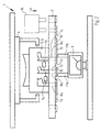
- FIG. 1 is a schematic view of a device 1 for equipping a board 2 with a resistance measuring device 3 is shown.
- the device 1 comprises, in addition to the resistance measuring device 3, a movable gripper 4, which has gripped a component 5.
- the component 5 is designed as an electromechanical switch 6 and is positioned by the gripper 4 on the board 2.
- the electromechanical switch 6 has three contacts 7a to 7c, which are aligned with holes 8a to 8c in the circuit board 2.
- the contacts 7a to 7c are designed as contact pins.
- the holes 8a to 8c pass through a carrier 9 and tracks 10 of the board 2.
- the movable resistance measuring device 3 of the device 1 is arranged below the board 2 and has two Contact pins 11a and 11b, with which formed by the conductor tracks 10 pads 12 of the board 2 are contacted.
- an electrical resistance 14 and between the contacts 7b and 7c an electrical resistance 15 is arranged in a transparent housing 13 of the electromechanical switch 6 between the contacts 7a and 7b.
- the gripper 4 has the component 5 or the electromechanical switch 6 inserted in an arrow direction z in the holes 8a to 8c of the board 2 and the switch 6 released.
- the resistance measuring device 3 By the resistance measuring device 3, a resistance measurement is now performed at two of the contact points 12 of the board 2, which are in communication with the contacts 7b and 7c of the switch 6.
- the resistance measuring device 3 is moved with its contact pins 11a and 11b against the corresponding conductor tracks 10 of the board 2. If the electrical resistors 14 and 15 of the switch 6 are correctly detected in two successive measurements, it is assumed that the circuit board 2 is properly equipped with the switch 6.
- a further component 16 is shown in addition, which is placed on the board 2, when the resistance measurement has confirmed a correct positioning of the switch 6.
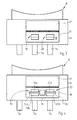
- FIG. 3 an electromechanical switch 6 is shown in a schematic side view.
- a housing 13 of the switch 6 has a pocket 17.
- two brackets 19, 20 are arranged.
- the clamp 19 is in electrical connection with a contact 7b of the switch 6 and the clamp 20 is in electrical connection with a contact 7c of the switch 6.
- the pocket 17 can be closed by a lid 21 shown unfolded.
- FIG. 4 is the one in the FIG. 3 shown switch 6 shown again, now between the Clamps 19 and 20, an electrical resistance 15 is seated.
- the resistor 15 can be clamped with its conductors 15a and 15b between jaws 19a, 19b and 20a, 20b of the clamps 19 and 20, respectively.
- the resistor 15 can be quickly assembled or disassembled and can be used in particular when needed at any time in the switch 6.
- a further pocket is arranged on a rear side of the housing 13 of the switch 6.
- FIG. 5 is a sectional side view of a variant of an electromechanical switch 6 is shown.
- the switch 6 has three contacts 7a, 7b and 7c.
- resistors 14 and 15 are arranged, which are measurable via the contacts 7a to 7c or connected to these, electrically conductive components.
- FIG. 6 is a lower part of the in the FIG. 5 shown switch 6 shown in a perspective view.
- the resistors 14 and 15 are glued in the switch 6 on sheets 21a, 21b and 21c, for example, with silver conductive adhesive.
- the plates 21a to 21c are in each case connected to one of the contacts 7a, 7b, 7c.
- the contacts 7a and 7b are connected through the resistor 14 and the contacts 7b and 7c through the resistor 15.
- the resistors are welded or soldered to the sheets.
- the in the Figures 5 and 6 shown resistors 14 and 15 are designed as so-called miniature resistors or SMD resistors. As a result, the resistors 14 and 15 need only minimal space in the switch 6.
- resistors in the electromechanical switch assume the function of measuring resistors.
- An arrangement of the or the measuring resistors is carried out according to the switch type.
- switches are, for example, changers or changeover switches, normally closed, normally open or center-0 switches.
- FIG. 7 a section of a punched grid 30 according to the invention is shown with located in a grid frame 31 receiving area 32.
- Each grid segment 33 which repeats periodically along the stamped grid 30, has mounting extensions 34 for mounting a switch blank 35, which provide a switch blank manufactured in previous manufacturing steps at a defined position within the stamped grid 30.
- the switch blank 35 is shown only schematically, without any resident on the switch blank arrangement of electrical conductors or mechanisms.
- the punched grid 30 has in the context of each lead frame segment 33 via positioning aid 36, which are in similar periodicity to the punched grid segment repetition.
- FIG. 8 shows another inventive punched grid 40, in this case in a stamped grid 30 by 90 ° rotated arrangement of the punched grid segments 41.
- the punched grid 40 also has a grid frame 42, receiving areas 43 and brackets 44, to which two resistors 45 are attached.
- prefabricated resistor arrangements can also be attached to the holders 44, which as a whole can be supplied to the method according to the invention for producing a component.
- punched grid 40 also has positioning aids 46.
- FIG. 9 shows the inventive arrangement 50, two punched grid 51 and 52, the punched grid 51 is moved along the working direction 53 after each step to a stamped grid segment, and the lead frame 52 along the working direction 54, perpendicular to the working direction 53 per work step each also moved to a stamped grid segment becomes.
- the punched grid 51 has resistances 56 held in the region in front of a junction area or processing area 55.
- the punched grid 52 has, in analogy, mounted switch blanks 57. In the processing area 55, positioning of the resistors 56 is positioned on the switch blank 57 using the positioning aid 58 in an area provided for attachment.
- the resistors 56 may have been brought by a previous step with their support in the appropriate position, which is necessary when the mounting position in the processing area 55 requires that the resistors 56 brought out of the lateral plane of the lead frame 51 out must be in order to reach the predetermined position for mounting in the field of the device can.
- the switch with resistors 59 can be further processed after leaving the merging region 55.
- a problem in the production of such switches is often the process of encapsulating the component, for example with plastic, if components, in particular resistors 45, have already been applied to the component in a previous working step.
- the different coefficients of thermal expansion lead in hot-molded plastic to the fact that joints between a switch blank 57 and the resistors 56 break open and are thus impaired in their function.
- a corresponding area for later attachment of resistors provided during encapsulation for example, a recess in the mold to be encapsulated, so by means of suitable pre-positioning of the resistors 56 in the lead frame 51, which can be done in a previous step, the resistors 56 in the recess area of Overmoulding be used, and then preferably fixed with a laser in one step on the switch blank 57, and at the same time be separated from the lead frame 51.
- the invention is not limited to illustrated or described embodiments. Rather, it includes developments of the invention within the scope of the patent claims.
- the invention also provides for the arrangement of other electronic components in the switch, the characteristics of which are detectable via the contacts of the switch.
Landscapes
- Engineering & Computer Science (AREA)
- Microelectronics & Electronic Packaging (AREA)
- Manufacturing & Machinery (AREA)
- Physics & Mathematics (AREA)
- Electromagnetism (AREA)
- Apparatuses And Processes For Manufacturing Resistors (AREA)
- Testing Electric Properties And Detecting Electric Faults (AREA)
- Manufacture Of Switches (AREA)
- Investigating Or Analyzing Materials By The Use Of Electric Means (AREA)
- Supply And Installment Of Electrical Components (AREA)
Abstract
Description
- "Verfahren zur Ermittlung eines Vorhandenseins eines Bauelements, Vorrichtung zum Bestücken einer Platine mit Bauelementen, Schalter sowie Herstellungsverfahren und Herstellungsanordnung".
- Die Erfindung betrifft ein Verfahren zur Ermittlung eines Vorhandenseins eines Bauelements nach Patentanspruch 1 und eine Vorrichtung zum Bestücken einer Platine mit Bauelementen nach Patentanspruch 4 sowie einen elektromechanischen Schalter nach Patentanspruch 6 und ein Verfahren zur Herstellung eines Bauelementes nach Anspruch 8 und eine Anordnung zur Herstellung eines Bauelements nach Anspruch 14.
- Der Erfindung liegt die Aufgabe zugrunde, ein Verfahren bzw. eine Vorrichtung zu entwickeln, welches bzw. welche es erlaubt das Vorhandensein eines elektrischen Bauteils während der Bestückung einer Platine festzustellen. Weiterhin ist es Aufgabe der Erfindung einen elektromechanischen Schalter vorzuschlagen, welcher für das erfindungsgemäße Verfahren bzw. die erfindungsgemäße Vorrichtung geeignet ist und entsprechend hergestellt wird.
- Diese Aufgabe wird bei einem Verfahren zur Ermittlung eines Vorhandenseins eines Bauelements durch die Merkmale des Anspruchs 1 und bei einer Vorrichtung zum Bestücken einer Platine durch die Merkmale des Anspruchs 4 gelöst sowie einen elektromechanischen Schalter mit den Merkmalen des Anspruchs 6 gelöst. Ein Verfahren sowie eine Anordnung zur Herstellung eines erfindungsgemäßen Bauelements sind durch die Merkmale der Ansprüche 8 sowie 14 gegeben. In den Unteransprüchen sind vorteilhafte und zweckmäßige Weiterbildungen angegeben.
- Das erfindungsgemäße Verfahren zur Ermittlung eines Vorhandenseins eines Bauelements, insbesondere eines elektromechanischen Schalters auf einer zu bestückenden Platine umfasst die folgenden Schritte: Bestückung der Platine mit dem Bauelement, Durchführen wenigstens einer Widerstandsmessung zwischen Kontaktstellen der Platine, welche für eine Kontaktierung des Bauelements vorgesehen sind, und Fortsetzung der Bestückung der Platine mit weiteren Bauelementen. Hierdurch kann auch bei komplexen Schaltungen auf einfache Weise sichergestellt werden, dass das fragliche Bauelement tatsächlich und korrekt bestückt worden ist. Die kurzzeitige Unterbrechung des Bestückungsvorgangs für einen Messvorgang ermöglicht es, ggf. eine Wiederholung der Bestückung vorzunehmen. Hierdurch kann vermieden werden, dass eine fehlgeschlagene Bestückung erst bemerkt wird, wenn die Platine bereits vollständig bestückt ist. Zu diesem Zeitpunkt ist eine Nachbestückung der Platine mit dem fehlenden Bauteil aufwendig und unter Umständen gar nicht mehr möglich.
- Gemäß dem erfindungsgemäßen Verfahren ist es vorgesehen, die Bestückung der Platine mit den weiteren Bauelementen fortzuführen, wenn durch die wenigstens eine Widerstandsmessung erwartete Widerstandswerte ermittelt werden bzw. die Bestückung der Platine mit den weiteren Bauelementen zu unterbrechen, wenn durch die wenigstens eine Widerstandsmessung der erwartete Widerstandswert oder die erwarteten Widerstandswerte nicht ermittelt werden. Diese Schritte ermöglichen bei minimalen Zusatzkosten eine frühzeitige Kontrolle der Platine zur Vermeidung von Ausschuss oder hohen Kosten für eine Nachbearbeitung.
- Das erfindungsgemäße Verfahren zur Herstellung eines Bauelements, insbesondere eines elektromechanischen Schalters, wobei das Bauelement mindestens einen elektrischen Widerstand zwischen wenigstens zwei Kontaktstellen umfasst, nutzt die Anbringung des Bauelements, insbesondere des elektromechanischen Schalters und mindestens des einen anzubringenden Widerstands in jeweils einem Stanzgitter, wobei in einem ersten Verfahrensschritt die jeweiligen Stanzgitter derart in eine überdeckende Positionierung gebracht werden, dass eine verarbeitungsgemäße Positionierung des mindestens einen Widerstand im zur Anbringung vorgesehenen Bereich am Bauelements erfolgt. Durch eine derartige Positionierung wird erreicht, dass entweder einzelne Widerstände oder auch auf Trägern angebrachte Widerstandsanordnungen relativ zum Herstellungsrohling eines Bauelements wie beispielsweise eines elektromechanischen Schalters bereits in der verarbeitungsgemäßen Position vorliegen, so dass ein positionierender Bestückungsvorgang, wie beispielsweise ein Bestückungsroboter entbehrlich wird. Vorteilhaft am vorliegenden Verfahren ist, dass am Schalterrohling entsprechende Ausnehmungen vorgesehen sein können, welche in ihrer Position der angestrebten überdeckenden Positionierung der Widerstände entsprechen, so dass diese im Bereich der Ausnehmungen am Bauelement angebracht werden können.
- In einer vorteilhaften Weiterbildung des Verfahrens werden die Stanzgitter vor dem Verarbeitungsschritt durch Positionierhilfen relativ zueinander positioniert und gegebenenfalls fixiert, sodann vorzugsweise in einem Arbeitsschritt sowohl die Anbringung des mindestens einen Widerstands als auch die Abtrennung vom Stanzgitter des Widerstands vorgenommen. Vorzugsweise kann auch eine Vorpositionierung der im jeweiligen Stanzgitter gehaltenen Bestandteile in einem vorhergehenden Arbeitsschritt, insbesondere eine Vorpositionierung des mindestens einen Widerstands oder einer Widerstandsanordnung auf einem Träger, erfolgen.
- Eine erfindungsgemäße Anordnung zur Herstellung eines Bauelements, insbesondere eines elektromagnetischen Schalters weist Anordnungen von Schalterrohlingen in einer ersten Matrix, vorzugsweise in einem ersten Stanzgitter auf, und Anordnungen von elektrischen Widerständen in Segmenten einer zweiten Matrix, insbesondere eines zweiten Stanzgitters, wobei die Matrizen derart relativ zueinander geführt sind, dass zumindest in einem überlappenden Teilbereich eine direkte Anbringung bzw. Montage mindestens eines Widerstands oder vorzugsweise einer Widerstandsanordnung gegebenenfalls auch auf einem Träger, auf mindestens einem Schalterrohling, vorzugsweise in vorgesehenen Aussparungen, durch Montagemittel ermöglicht ist.
- Die erfindungsgemäße Vorrichtung zum Bestücken einer Platine mit Bauelementen sieht eine Widerstandsmesseinrichtung vor, durch welche der elektrische Widerstand wenigstens eines Bauelements nach dem Bestücken an Kontaktstellen der Platine erfassbar ist, wobei die Erfassung des elektrischen Widerstands vor der Beendigung des Bestückungsvorgangs durchführbar ist. Hierdurch kann eine fehlerhafte Bestückung durch die Vorrichtung frühzeitig im Fertigungsvorgang erkannt werden.
- Erfindungsgemäß ist das zu überprüfende Bauelement als elektromechanischer Schalter ausgeführt. Bei derartigen Bauelementen besteht eine erhöhte Gefahr, dass diese nicht oder nicht korrekt auf die Platine gesetzt werden.
- Der erfindungsgemäße elektromechanische Schalter mit Kontakten zur Kontaktierung einer Platine, ist nachträglich, vorzugsweise nach vorgenanntem Verfahren, mit wenigstens einem elektrischen Widerstand bestückbar, wobei der elektrische Widerstand zwischen wenigstens zwei Kontakten des elektromechanischen Schalters angeordnet ist. Hierdurch ist eine unkomplizierte Logistik gewährleistet, da der Schalter erst unmittelbar vor dem Verbau des Gehäuses bei Bedarf mit einem oder mehreren Widerständen versehen werden kann.
- Weiterhin sieht die Erfindung vor, den elektrischen Widerstand innerhalb eines Gehäuses des elektromechanischen Schalters anzuordnen. Hierdurch bleibt die Baugröße des Schalters unverändert, somit kann ein derartiger Schalter auch bei bestehenden Schaltungsanordnungen ohne Veränderung des Platinendesigns verwendet werden. Weiterhin müssen der oder die Widerstände nicht zusätzlich, zum Beispiel durch Vergießen, geschützt werden, da der oder die Widerstände im Inneren des Schalters angeordnet sind.
- Weitere Einzelheiten der Erfindung werden in der Zeichnung anhand von schematisch dargestellten Ausführungsbeispielen beschrieben.
- Hierbei zeigt:
- Figur 1
- eine schematische Ansicht einer Vorrichtung zur Bestückung einer Platine, vor dem Bestücken der Platine mit dem Bauelement;
- Figur 2
- eine weitere Ansicht der aus der
Figur 1 bekannten Vorrichtung, wobei das Bauelement auf die Platine aufgesetzt ist und die Widerstandsmesseinrichtung misst; - Figur 3
- eine schematische Seitenansicht eines elektromechanischen Schalters mit einer Tasche zum nachträglichen Einsetzen eines Widerstands;
- Figur 4
- eine weitere schematische Seitenansicht des aus der
Figur 3 bekannten elektromechanischen Schalters, wobei in die Tasche ein Widerstand eingesetzt ist; - Figur 5
- eine geschnittene Seitenansicht einer Ausführungsvariante eines elektromechanischen Schalters mit Widerständen und
- Figur 6
- eine perspektivische Ansicht eines unteren Teils des in der
Figur 5 gezeigten elektromechanischen Schalters. - Figur 7
- zeigt einen Ausschnitt aus einem erfindungsgemäßen Stanzgitter mit Schalterrohlingen.
- Figur 8
- zeigt einen Ausschnitt aus einem erfindungsgemäßen Stanzgitter mit Widerständen.
- Figur 9
- zeigt einen erfindungsgemäßen Ausschnitt aus überkreuzt laufenden Stanzgittern im Vereinigungsbereich.
- In der
Figur 1 ist eine schematische Ansicht einer Vorrichtung 1 zur Bestückung einer Platine 2 mit einer Widerstandsmesseinrichtung 3 dargestellt. Die Vorrichtung 1 umfasst neben der Widerstandmesseinrichtung 3 einen verfahrbaren Greifer 4, welcher ein Bauelement 5 gegriffen hat. Das Bauelement 5 ist als elektromechanischer Schalter 6 ausgeführt und wird von dem Greifer 4 über der Platine 2 positioniert. Der elektromechanische Schalter 6 weist drei Kontakte 7a bis 7c auf, welche auf Bohrungen 8a bis 8c in der Platine 2 ausgerichtet sind. Die Kontakte 7a bis 7c sind als Kontaktstifte ausgeführt. Die Bohrungen 8a bis 8c durchlaufen eine Träger 9 und Leiterbahnen 10 der Platine 2. Die verfahrbare Widerstandsmesseinrichtung 3 der Vorrichtung 1 ist unterhalb der Platine 2 angeordnet und weist zwei Kontaktstifte 11a und 11b auf, mit welchen durch die Leiterbahnen 10 gebildete Kontaktstellen 12 der Platine 2 kontaktierbar sind. In einem durchsichtig dargestellten Gehäuse 13 des elektromechanischen Schalters 6 ist zwischen den Kontakten 7a und 7b ein elektrischer Widerstand 14 und zwischen den Kontakten 7b und 7c ein elektrischer Widerstand 15 angeordnet. - In der
Figur 2 hat der Greifer 4 das Bauelement 5 bzw. den elektromechanischen Schalter 6 in eine Pfeilrichtung z in die Bohrungen 8a bis 8c der Platine 2 eingeschoben und den Schalter 6 losgelassen. Durch die Widerstandsmesseinrichtung 3 wird nun an zwei der Kontaktstellen 12 der Platine 2, welche mit den Kontakten 7b und 7c des Schalters 6 in Verbindung stehen, eine Widerstandsmessung durchgeführt. Hierzu wird die Widerstandsmesseinrichtung 3 mit ihren Kontaktstiften 11a und 11b gegen die entsprechenden Leiterbahnen 10 der Platine 2 gefahren. Sofern die elektrischen Widerstände 14 und 15 des Schalters 6 in zwei aufeinander folgenden Messungen korrekt erfasst werden, wird von einer ordnungsgemäßen Bestückung der Platine 2 mit dem Schalter 6 ausgegangen. In derFigur 2 ist ergänzend noch ein weiteres Bauelement 16 dargestellt, welches auf die Platine 2 gesetzt wird, wenn die Widerstandmessung eine korrekte Positionierung des Schalters 6 bestätigt hat. - In der
Figur 3 ist ein elektromechanischer Schalter 6 in schematischer Seitenansicht dargestellt. Ein Gehäuse 13 des Schalters 6 weist eine Tasche 17 auf. In einem Innenraum 18 der Tasche 17 sind zwei Klammern 19, 20 angeordnet. Die Klammer 19 steht in elektrischer Verbindung mit einem Kontakt 7b des Schalters 6 und die Klammer 20 steht in elektrischer Verbindung mit einem Kontakt 7c des Schalters 6. Die Tasche 17 ist durch einen aufgeklappt dargestellten Deckel 21 verschließbar. In derFigur 4 ist der in derFigur 3 gezeigte Schalter 6 nochmals dargestellt, wobei nunmehr zwischen den Klammern 19 und 20 ein elektrischer Widerstand 15 sitzt. Der Widerstand 15 kann mit seinen Leitern 15a und 15b zwischen Backen 19a, 19b bzw. 20a, 20b der Klammern 19 bzw. 20 eingeklemmt werden. Hierdurch ist der Widerstand 15 rasch montierbar bzw. demontierbar und kann insbesondere bei Bedarf zu einem beliebigen Zeitpunkt in den Schalter 6 eingesetzt werden. Um zwischen einem Kontakt 7a und dem Kontakt 7b einen weiteren Widerstand anzuordnen ist auf einer Rückseite des Gehäuses 13 des Schalters 6 eine weitere, hier nicht sichtbare Tasche angeordnet. - In der
Figur 5 ist eine geschnittene Seitenansicht einer Ausführungsvariante eines elektromechanischen Schalters 6 dargestellt. Der Schalter 6 weist drei Kontakte 7a, 7b und 7c auf. In einem Gehäuse 13 bzw. Sockel des Schalters 6 sind wiederum Widerstände 14 bzw. 15 angeordnet, welche über die Kontakte 7a bis 7c bzw. über mit diesen verbundene, elektrisch leitfähige Bauteile messbar sind. - In der
Figur 6 ist ein unterer Teil des in derFigur 5 gezeigten Schalters 6 in perspektivischer Ansicht dargestellt. Die Widerstände 14 und 15 sind im Schalter 6 auf Blechen 21a, 21b bzw. 21c beispielsweise mit Silberleitkleber aufgeklebt. Die Bleche 21a bis 21c stehen jeweils mit einem der Kontakte 7a, 7b, 7c in Verbindung. Somit sind die Kontakte 7a und 7b durch den Widerstand 14 und die Kontakte 7b und 7c durch den Widerstand 15 verbunden. Gemäß nicht dargestellten Ausführungsvarianten sind die Widerstände auf die Bleche aufgeschweißt oder aufgelötet. Die in denFiguren 5 und6 gezeigten Widerständer 14 und 15 sind als sogenannte Miniaturwiderstände oder SMD-Widerstände ausgeführt. Hierdurch benötigen die Widerständer 14 und 15 im Schalter 6 nur minimale Bauräume. - Eine spätere negative Beeinträchtigung einer auf der Platine angeordneten elektronischen Schaltung ist durch die Wahl von hochohmigen Widerständen praktisch ausgeschlossen. Die Widerstände in dem elektromechanischen Schalter übernehmen die Funktion von Messwiderständen. Eine Anordnung des oder der Messwiderstände erfolgt entsprechend dem Schaltertyp. Unter Schaltern sind im Sinne der Erfindung beispielsweise Wechsler bzw. Wechselschalter, Öffner, Schließer oder Mitte-0-Schalter zu verstehen.
- In
Figur 7 ist ein Ausschnitt aus einem erfindungsgemäßen Stanzgitter 30 mit in einem Gitterrahmen 31 befindlichen Aufnahmebereich 32 dargestellt. Jedes Gittersegment 33, welches sich periodisch entlang des Stanzgitters 30 wiederholt, weist Halterungsfortsätze 34 zur Halterung eines Schalterrohlings 35 auf, welche einen in vorhergehenden Herstellungsschritten hergestellten Schalterrohling an einer definierten Position innerhalb des Stanzgitters 30 bereitstellen. In vorliegender Figur ist der Schalterrohling 35 nur schematisch dargestellt, ohne jedweilige auf dem Schalterrohling befindliche Anordnung an elektrischen Leiterbahnen oder Mechaniken. Das Stanzgitter 30 verfügt im Rahmen jedes Stanzgittersegments 33 über Positionierhilfe 36, welche sich in ähnlicher Periodizität zur Stanzgittersegmentwiederholung befinden. -
Figur 8 zeigt ein weiteres erfindungsgemäßes Stanzgitter 40, vorliegend in einer zum Stanzgitter 30 um 90° gedrehten Anordnung der Stanzgittersegmente 41. Das Stanzgitter 40 weist ebenfalls einen Gitterrahmen 42 auf, Aufnahmebereiche 43 sowie Halterungen 44, an welchen vorliegend zwei Widerstände 45 angebracht sind. In einer nicht gezeigten Ausführung können an den Halterungen 44 auch vorgefertigte Widerstandsanordnungen angebracht sein, welche als Ganzes dem erfindungsgemäßen Verfahren zur Herstellung eines Bauelements zugeführt werden können. Ebenso wie das Stanzgitter 30 weist auch das Stanzgitter 40 Positionierhilfen 46 auf. -
Figur 9 zeigt die erfindungsgemäße Anordnung 50, zweier Stanzgitter 51 sowie 52, wobei das Stanzgitter 51 entlang der Arbeitsrichtung 53 nach jedem Arbeitsschritt um ein Stanzgittersegment fortbewegt wird, und das Stanzgitter 52 entlang der Arbeitsrichtung 54, rechtwinklig zur Arbeitsrichtung 53 pro Arbeitsschritt jeweils auch um ein Stanzgittersegment fortbewegt wird. Das Stanzgitter 51 weist vorliegend im Bereich vor einem Vereinigungsbereich bzw. Verarbeitungsbereich 55 gehalterte Widerstände 56 auf. Das Stanzgitter 52 weist in Analogie dazu gehalterte Schalterrohlinge 57 auf. Im Verarbeitungsbereich 55 wird unter Nutzung der Positionierhilfe 58 eine Positionierung der Widerstände 56 in einem zur Anbringung vorgesehenen Bereich am Schalterrohling 57 positioniert. Durch vorliegend nicht gezeigte Montagemittel, wie beispielsweise durch Lasermontagemittel, erfolgt in einem Arbeitsschritt sowohl die Abtrennung der Widerstände 56 aus dem Stanzgitter 51 als auch die Anbringung der Widerstände 56 auf dem Schalterrohling 57, welcher nach wie vor im Stanzgitter 52 gehalten wird. In einer nicht gezeigten Ausführung können die Widerstände 56 durch einen vorher gegangenen Arbeitsschritt mit ihrer Halterung in entsprechende Position gebracht worden sein, was dann notwendig ist, wenn die Montageposition im Verarbeitungsbereich 55 verlangt, dass die Widerstände 56 aus der lateralen Ebene des Stanzgitters 51 heraus gebracht werden müssen, um die vorgegebene Position zur Anbringung im Bereich des Bauelements erreichen zu können. Entlang der Arbeitsrichtung 54 kann nach Verlassen des Vereinigungsbereich 55 der Schalter mit Widerständen 59 weiter verarbeitet werden. - Ein Problem bei der Herstellung derartiger Schalter stellt oftmals der Vorgang des Umspritzen des Bauelements beispielsweise mit Kunststoff dar, wenn auf dem Bauelement bereits in einem vorhergegangenen Arbeitsschritt Bauteile, insbesondere Widerstände 45 aufgebracht wurden. Die unterschiedlichen thermischen Ausdehnungskoeffizienten führen bei Umspritzen mit heißem Kunststoff dazu, dass Verbindungsstellen zwischen einem Schalterrohling 57 und den Widerständen 56 aufbrechen und so in ihrer Funktion beeinträchtigt sind. Wird beim Umspritzen nun ein entsprechender Bereich zur nachträglichen Anbringung von Widerständen vorgesehen, beispielsweise eine Aussparung in der zu umspritzenden Form, so können mittels geeigneter Vorpositionierung der Widerstände 56 im Stanzgitter 51, welche in einem vorhergehenden Arbeitsschritt erfolgen kann, die Widerstände 56 in den Aussparungsbereich der Umspritzung eingesetzt werden, und sodann vorzugsweise mit einem Laser in einem Arbeitsschritt am Schalterrohling 57 befestigt werden, und gleichzeitig aus dem Stanzgitter 51 herausgetrennt werden.
- Die Erfindung ist nicht auf dargestellte oder beschriebene Ausführungsbeispiele beschränkt. Sie umfasst vielmehr Weiterbildungen der Erfindung im Rahmen der Schutzrechtsansprüche. Insbesondere sieht die Erfindung auch die Anordnung anderer elektronischer Bauteile im Schalter vor, deren Kenngrößen über die Kontakte des Schalters erfassbar sind.
-
- 1
- Vorrichtung
- 2
- Platine
- 3
- Widerstandsmesseinrichtung
- 4
- Greifer
- 5
- Bauelement
- 6
- elektromechanischer Schalter
- 7a - 7c
- Kontakt von 6
- 8a - 8c
- Bohrung in 2
- 9
- Träger von 2
- 10
- Leiterbahn von 2
- 11a, 11b
- Kontaktstift von 3
- 12
- Kontaktstelle von 2
- 13
- Gehäuse von 6
- 14
- elektrischer Widerstand
- 15
- elektrischer Widerstand
- 15a, 15b
- Leiter von 15
- 16
- weiteres Bauelement zur Anordnung auf 2
- 17
- Tasche in 6
- 18
- Innenraum von 17
- 19
- Klammer zur Kontaktierung von 15
- 19a, 19b
- Backe von 19
- 20
- Klammer zur Kontaktierung von 15
- 20a, 20b
- Backe von 20
- 21a - 21c
- Blech verbunden mit 7a bzw. 7b bzw. 7c
- z
- Pfeilrichtung
- 30
- Stanzgitter längs
- 31
- Gitterrahmen
- 32
- Aufnahmebereich
- 33
- Stanzgittersegment
- 34
- Halterungsfortsätze
- 35
- Schalterrohling
- 36
- Positionshilfen (Rasterlöcher)
- 40
- Stanzgitter quer
- 41
- Stanzgittersegment
- 42
- Gitterrahmen
- 43
- Aufnahmebereich
- 44
- Halterung
- 45
- Widerstand
- 46
- Positionierhilfen
- 50
- Anordnung
- 51
- Stanzgitter "R"
- 52
- Stanzgitter "SW"
- 53
- Arbeitsrichtung
- 54
- Arbeitsrichtung
- 55
- Vereinigungsbereich
- 56
- Widerstände
- 57
- Schalterrohlinge
- 58
- Positionierhilfe
- 59
- Schalter mit Widerständen
Claims (15)
- Verfahren zur Ermittlung eines Vorhandenseins eines Bauelements (5), insbesondere eines elektromechanischen Schalters (6) auf einer zu bestückenden Platine (2), dadurch gekennzeichnet, dass die Platine (2) mit dem Bauelement (5, 6) bestückt wird, dass nach der Bestückung der Platine (2) mit dem Bauelement (5, 6) und vor einer Fortsetzung der Bestückung der Platine (2) mit weiteren Bauelementen (16) und /oder einer sonstigen Weiterbearbeitung der Platine (2) wenigstens eine Widerstandsmessung zwischen Kontaktstellen (12) der Platine (2) durchgeführt wird, wobei die Kontaktstellen (12) für eine Kontaktierung des Bauelements (5, 6) vorgesehen sind.
- Verfahren nach Anspruch 1, dadurch gekennzeichnet, dass die Bestückung der Platine (2) mit den weiteren Bauelementen (16) und/oder die sonstige Weiterbearbeitung der Platine (2) fortgeführt wird, wenn durch die wenigstens eine Widerstandsmessung erwartete Widerstandswerte ermittelt werden.
- Verfahren nach einem der vorhergehenden Ansprüche, dadurch gekennzeichnet, dass die Bestückung der Platine (2) mit den weiteren Bauelementen (16) und/oder die sonstige Weiterbearbeitung der Platine (2) unterbrochen wird, wenn durch die wenigstens eine Widerstandsmessung der erwartete Widerstandswert oder die erwarteten Widerstandswerte nicht ermittelt werden.
- Vorrichtung (1) zum Bestücken einer Platine (2) mit Bauelementen (5), dadurch gekennzeichnet, dass durch eine Widerstandsmesseinrichtung (3) der Vorrichtung (1) der elektrische Widerstand wenigstens eines Bauelements (5) nach dem Bestücken der Platine (2) mit dem Bauelement (5) an Kontaktstellen (12) der Platine (2) erfassbar ist, wobei die Erfassung des elektrischen Widerstands vor der Beendigung des Bestückungsvorgangs und/oder von einer sonstigen Weiterbearbeitung der Platine (2) durchführbar ist.
- Vorrichtung nach Anspruch 4, dadurch gekennzeichnet, dass das Bauelement (5) als elektromechanischer Schalter (6) ausgeführt ist.
- Elektromechanischer Schalter (6) mit Kontakten (7a - 7c) zur Kontaktierung einer Platine (2), dadurch gekennzeichnet, dass der elektromechanische Schalter (6) nach seiner Herstellung und/oder bei einer Weiterbearbeitung der Platine (2) mit wenigstens einem elektrischen Widerstand (14, 15) bestückbar ist, wobei der elektrische Widerstand (14, 15) zwischen wenigstens zwei Kontakten (7a, 7b, 7c) des elektromechanischen Schalters (6) angeordnet ist.
- Elektromechanischer Schalter (6) nach Anspruch 6, dadurch gekennzeichnet, dass der elektrische Widerstand (14, 15) innerhalb eines Gehäuses (13) des elektromechanischen Schalters (6) angeordnet ist.
- Verfahren zur Herstellung eines Bauelements, insbesondere eines elektromechanischen Schalters (59), wobei das Bauelement mindestens einen elektrischen Widerstand (45) zwischen wenigstens zwei Kontaktstellen umfasst, dadurch gekennzeichnet, dass das Bauelement, insbesondere eine Kontaktanordnung für den elektromechanischen Schalter (59), und mindestens der eine anzubringende Widerstand (45) jeweils in einem Stanzgitter (30, 40) derart angeordnet sind, dass bei überdeckender Positionierung der Stanzgitter (30, 40) eine verarbeitungsgemäße Positionierung (55) des mindestens einen Widerstands (45) im zur Anbringung vorgesehenen Bereich am Bauelement erfolgt.
- Verfahren nach Anspruch 8, dadurch gekennzeichnet, dass die Stanzgittern (30, 40) mittels Positionierhilfen (36, 46, 58), insbesondere Rasterlöchern zueinander positioniert und gegebenenfalls fixiert werden.
- Verfahren nach Anspruch 8 oder 9, dadurch gekennzeichnet, dass die Anbringung des mindestens einen Widerstands (45) auf der Kontaktanordnung des Schalters (57) im Arbeitsschritt der Abtrennung von seinem Stanzgitter erfolgt.
- Verfahren nach Anspruch 8, 9 oder 10, dadurch gekennzeichnet, dass die Anbringung des mindestens einen Widerstands (45) sowie dessen Abtrennung aus seinem Stanzgitter auf der Kontaktanordnung des Schalters (57) mittels Laserstrahlung erfolgt.
- Verfahren nach einem der Ansprüche 8-11, dadurch gekennzeichnet, dass die Stanzgitter (30, 40) entlang jeweils einer Vorschubrichtung (53, 54) geführt werden, wobei die Vorschubrichtungen parallel oder sich kreuzend, insbesondere rechtwinklig verlaufen.
- Verfahren nach einem der Ansprüche 8-12, dadurch gekennzeichnet, dass eine Vorpositionierung der im jeweiligen Stanzgitter (30, 40) gehaltenen Bestandteile (35, 45), insbesondere eine Vorpositionierung des mindestens einen Widerstands (45), in einem vorhergehenden Arbeitsschritt erfolgt.
- Verfahren nach einem der Ansprüche 8-13, wobei in einem ersten Stanzgitter (51) entlang einer ersten Vorschubrichtung (53) mehrere Widerstände (45) in einem vorgesehenen Abstand pro Stanzgittersegment (41) angeordnet sind, und wobei in einem zweiten Stanzgitter (52) entlang einer zweiten Vorschubrichtung (54) eine gegebenenfalls mit einem Sockel umspritzte Kontaktanordnung für einen Schalter (57) pro Stanzgittersegment (33) angeordnet ist, dadurch gekennzeichnet, dass die Stanzgittersegmente (33, 41) entlang ihrer Vorschubrichtungen (53, 54) in überdeckende Positionierung (55), vorzugsweise mit einer Positionierungshilfe (58), insbesondere einem Raster, gebracht werden, und in einem daraus entstehenden Vereinigungsbereich (55) die Widerstände (45) in einem Arbeitsschritt auf dem Schalter (57) im zur Anbringung vorgesehenen Bereich angebracht werden.
- Anordnung zur Herstellung eines Bauelements, insbesondere eines elektromechanischen Schalters (59) nach Anspruch 6, dadurch gekennzeichnet, dass Schalterrohlinge (53, 57) fortlaufend in Segmenten (33) einer ersten Matrix, insbesondere eines ersten Stanzgitters (52) angeordnet sind, und dass elektrische Widerstände (45) in Segmenten (41) einer zweiten Matrix, insbesondere eines zweiten Stanzgitters (51) angeordnet sind, wobei die Matrizen derart relativ zueinander geführt sind, dass zumindest in einem überlappenden Teilbereich (55) eine direkte Anbringung bzw. Montage mindestens eines Widerstands (45) auf mindestens einem Schalterrohling (57) durch Montagemittel möglich ist.
Applications Claiming Priority (2)
| Application Number | Priority Date | Filing Date | Title |
|---|---|---|---|
| DE102007018207 | 2007-04-16 | ||
| DE102007018376 | 2007-04-17 |
Publications (3)
| Publication Number | Publication Date |
|---|---|
| EP1986204A2 true EP1986204A2 (de) | 2008-10-29 |
| EP1986204A3 EP1986204A3 (de) | 2010-11-03 |
| EP1986204B1 EP1986204B1 (de) | 2017-07-12 |
Family
ID=39651376
Family Applications (1)
| Application Number | Title | Priority Date | Filing Date |
|---|---|---|---|
| EP08007406.5A Active EP1986204B1 (de) | 2007-04-16 | 2008-04-16 | Verfahren zur Herstellung eines elektromechanischen Schalters |
Country Status (3)
| Country | Link |
|---|---|
| EP (1) | EP1986204B1 (de) |
| DE (1) | DE102008019324B4 (de) |
| ES (1) | ES2641583T3 (de) |
Cited By (1)
| Publication number | Priority date | Publication date | Assignee | Title |
|---|---|---|---|---|
| CN113518926A (zh) * | 2019-03-07 | 2021-10-19 | 三菱电机株式会社 | 用于监测功率模块的半导体的连接的方法和设备 |
Families Citing this family (1)
| Publication number | Priority date | Publication date | Assignee | Title |
|---|---|---|---|---|
| DE102010042323A1 (de) | 2010-10-12 | 2012-04-12 | Zf Friedrichshafen Ag | Widerstandsbeschaltet überwachbare Baugruppe |
Citations (5)
| Publication number | Priority date | Publication date | Assignee | Title |
|---|---|---|---|---|
| US4168404A (en) | 1976-11-17 | 1979-09-18 | Amp Incorporated | Impedance programming dip switch assembly |
| EP0117984A1 (de) | 1983-02-04 | 1984-09-12 | New Ohto Co.,Ltd. | Aufbau eines vereinfachten elektrischen Schalters |
| DE3702346A1 (de) | 1986-01-29 | 1987-07-30 | Copal Electronics | Dip-drehschalter |
| DE4107896A1 (de) | 1991-03-12 | 1992-09-17 | Siemens Ag | Schalter, insbesondere codierschalter, mit integriertem wiederstand und verfahren zu dessen herstellung |
| US20030136656A1 (en) | 2002-01-23 | 2003-07-24 | Dunne John Edmund | Switch assembly employing an external customizing printed circuit board |
Family Cites Families (12)
| Publication number | Priority date | Publication date | Assignee | Title |
|---|---|---|---|---|
| SE454308B (sv) * | 1980-02-14 | 1988-04-18 | Labinal | Forfarande for framstellning av en smeltsekring samt maskin for utforande av det nemnda forfarandet |
| US4463310A (en) * | 1980-07-11 | 1984-07-31 | Rca Corporation | Apparatus for detecting the presence of components on a printed circuit board |
| CA1220806A (en) * | 1981-12-02 | 1987-04-21 | David J. Gingerich | Sealed electrical contact assembly and electrical switch made therefrom |
| US4557043A (en) * | 1983-12-05 | 1985-12-10 | Rca Corporation | Component lead processing apparatus |
| JPS63195772U (de) * | 1987-06-05 | 1988-12-16 | ||
| DE8715341U1 (de) * | 1987-11-19 | 1988-02-11 | Kübler, Wolfgang, Zug | Schaltungselement |
| US4947112A (en) * | 1989-07-28 | 1990-08-07 | At&T Bell Laboratories | Apparatus and method for testing printed circuit boards |
| US5101152A (en) | 1990-01-31 | 1992-03-31 | Hewlett-Packard Company | Integrated circuit transfer test device system utilizing lateral transistors |
| DK9300498U3 (da) | 1993-11-11 | 1993-12-24 | N L Elektronik V Niels Larsen | Attenuator fortrinsvis til audiosignaler |
| US6683449B1 (en) * | 2000-10-06 | 2004-01-27 | Dell Products, L.P. | Apparatus and method for detecting a mechanical component on a computer system substrate |
| JP4230754B2 (ja) | 2002-11-05 | 2009-02-25 | 日本無線株式会社 | 部品実装状態検出方法及び電子機器組立体 |
| TWI227099B (en) * | 2003-03-31 | 2005-01-21 | Siliconware Precision Industries Co Ltd | Chip carrier for testing electric performance of passive components and method for testing same |
-
2008
- 2008-04-16 ES ES08007406.5T patent/ES2641583T3/es active Active
- 2008-04-16 EP EP08007406.5A patent/EP1986204B1/de active Active
- 2008-04-16 DE DE102008019324.0A patent/DE102008019324B4/de not_active Expired - Fee Related
Patent Citations (5)
| Publication number | Priority date | Publication date | Assignee | Title |
|---|---|---|---|---|
| US4168404A (en) | 1976-11-17 | 1979-09-18 | Amp Incorporated | Impedance programming dip switch assembly |
| EP0117984A1 (de) | 1983-02-04 | 1984-09-12 | New Ohto Co.,Ltd. | Aufbau eines vereinfachten elektrischen Schalters |
| DE3702346A1 (de) | 1986-01-29 | 1987-07-30 | Copal Electronics | Dip-drehschalter |
| DE4107896A1 (de) | 1991-03-12 | 1992-09-17 | Siemens Ag | Schalter, insbesondere codierschalter, mit integriertem wiederstand und verfahren zu dessen herstellung |
| US20030136656A1 (en) | 2002-01-23 | 2003-07-24 | Dunne John Edmund | Switch assembly employing an external customizing printed circuit board |
Cited By (2)
| Publication number | Priority date | Publication date | Assignee | Title |
|---|---|---|---|---|
| CN113518926A (zh) * | 2019-03-07 | 2021-10-19 | 三菱电机株式会社 | 用于监测功率模块的半导体的连接的方法和设备 |
| CN113518926B (zh) * | 2019-03-07 | 2024-04-12 | 三菱电机株式会社 | 用于监测功率模块的半导体的连接的方法和设备 |
Also Published As
| Publication number | Publication date |
|---|---|
| DE102008019324A1 (de) | 2008-11-06 |
| DE102008019324B4 (de) | 2022-10-06 |
| EP1986204B1 (de) | 2017-07-12 |
| EP1986204A3 (de) | 2010-11-03 |
| ES2641583T3 (es) | 2017-11-10 |
Similar Documents
| Publication | Publication Date | Title |
|---|---|---|
| EP2692025B1 (de) | Modulare elektrische steckverbinderanordnung | |
| DE102007020882B4 (de) | Einrichtung zur Überprüfung der Befestigung einer Leiterbahnplatte an einem Träger | |
| DE102016122577A1 (de) | Leiterplatte und Verfahren zur Herstellung der Leiterplatte | |
| EP3109951B1 (de) | Elektrische baueinheit, verbindungseinheit mit mindestens einer elektrischen baueinheit, fahrzeug damit und verfahren zum herstellen einer elektrischen baueinheit | |
| DE102016203560B4 (de) | Aktoranordnung mit einem Sensormodul für einen Aktor mit verschiebbarem Anker | |
| DE102006027748A1 (de) | Leiterplatte und Verfahren zur Herstellung einer lötfreien elektrischen Verbindung | |
| DE102008019324B4 (de) | Verfahren zur Ermittlung eines Vorhandenseins eines Bauelements, Vorrichtung zum Bestücken einer Platine mit Bauelementen, Schalter sowie Herstellungsverfahren und Herstellungsanordnung | |
| DE102012010722B4 (de) | Kraftfahrzeug-Türschlossgehäuse und Verfahren zu seiner Herstellung | |
| EP1654744B1 (de) | Kondensatormodul und verfahren zu dessen herstellung | |
| EP1251358B1 (de) | Vorrichtung und Verfahren zum Herstellen und Testen von Elektronik-Baugruppen | |
| DE102013209435A1 (de) | Steckerverbindung mit einem zur Vermeidung von Spänen optimierten Führungselement | |
| DE102007005877A1 (de) | Verbindungssystem für Leiterplatten | |
| DE102014109036A1 (de) | Elektrische Verbindungsvorrichtung mit zwei Bereichen für eine Leiterplatte, elektronisches Gerät, Kraftfahrzeug und Herstellungsverfahren | |
| DE102011054105A1 (de) | Verbindungsleiterplatte | |
| EP2679969B1 (de) | Vorrichtung zur Erfassung der Temperatur in einem Raum und ein Verfahren zur Herstellung einer solchen Vorrichtung | |
| DE102013214478A1 (de) | Nutzen mit mehreren Leiterplatten und Verfahren zu seiner Herstellung | |
| DE102009048527B4 (de) | Anordnung von mehreren Schaltungsträgern und Verfahren zur Herstellung einer derartigen Anordnung | |
| DE202025104917U1 (de) | Neuartiger Insassen-Drucksensor | |
| EP0762549A2 (de) | Elektrischer Verbinder | |
| DE102012108859A1 (de) | Montagevorrichtung | |
| DE102009054236A1 (de) | Verfahren zum Herstellen eines spritzgegossenen Schaltungsträgers | |
| DE102017210979B4 (de) | Verfahren zur Herstellung eines elektrischen Bauteils und elektrisches Bauteil | |
| DE102017214780A1 (de) | Sensorbauteil, Vormontageanordnung für ein Sensorbauteil und Verfahren zur Herstellung eines Sensorbauteils | |
| DE20317036U1 (de) | Kabelsatzelement, insbesondere zur Anordnung auf einem Türmodul eines Kraftfahrzeugs | |
| EP2953436B1 (de) | Verfahren zum herstellen eines elektronischen verbindungselements |
Legal Events
| Date | Code | Title | Description |
|---|---|---|---|
| PUAI | Public reference made under article 153(3) epc to a published international application that has entered the european phase |
Free format text: ORIGINAL CODE: 0009012 |
|
| AK | Designated contracting states |
Kind code of ref document: A2 Designated state(s): AT BE BG CH CY CZ DE DK EE ES FI FR GB GR HR HU IE IS IT LI LT LU LV MC MT NL NO PL PT RO SE SI SK TR |
|
| AX | Request for extension of the european patent |
Extension state: AL BA MK RS |
|
| RIN1 | Information on inventor provided before grant (corrected) |
Inventor name: MATTES, CHRISTOPH Inventor name: HASSELBRINCK, INGO Inventor name: MORARIU, CONSTANTIN-ROMEO Inventor name: RIESENBERG, JENS Inventor name: HENGSTLER, HANS Inventor name: BEHR, VOLKER |
|
| PUAL | Search report despatched |
Free format text: ORIGINAL CODE: 0009013 |
|
| AK | Designated contracting states |
Kind code of ref document: A3 Designated state(s): AT BE BG CH CY CZ DE DK EE ES FI FR GB GR HR HU IE IS IT LI LT LU LV MC MT NL NO PL PT RO SE SI SK TR |
|
| AX | Request for extension of the european patent |
Extension state: AL BA MK RS |
|
| 17P | Request for examination filed |
Effective date: 20110502 |
|
| AKX | Designation fees paid |
Designated state(s): AT BE BG CH CY CZ DE DK EE ES FI FR GB GR HR HU IE IS IT LI LT LU LV MC MT NL NO PL PT RO SE SI SK TR |
|
| 17Q | First examination report despatched |
Effective date: 20111227 |
|
| GRAP | Despatch of communication of intention to grant a patent |
Free format text: ORIGINAL CODE: EPIDOSNIGR1 |
|
| RIC1 | Information provided on ipc code assigned before grant |
Ipc: H05K 3/20 20060101ALN20161005BHEP Ipc: H05K 13/04 20060101ALI20161005BHEP Ipc: H01H 11/00 20060101ALI20161005BHEP Ipc: H05K 13/08 20060101ALI20161005BHEP Ipc: G01R 31/28 20060101ALN20161005BHEP Ipc: H01H 9/02 20060101AFI20161005BHEP Ipc: H05K 3/30 20060101ALI20161005BHEP Ipc: H05K 3/22 20060101ALN20161005BHEP Ipc: H05K 1/02 20060101ALI20161005BHEP Ipc: H01C 1/01 20060101ALI20161005BHEP Ipc: H01H 1/58 20060101ALI20161005BHEP |
|
| STAA | Information on the status of an ep patent application or granted ep patent |
Free format text: STATUS: GRANT OF PATENT IS INTENDED |
|
| RIC1 | Information provided on ipc code assigned before grant |
Ipc: H05K 3/22 20060101ALN20161013BHEP Ipc: H05K 13/04 20060101ALI20161013BHEP Ipc: H01H 1/58 20060101ALI20161013BHEP Ipc: H05K 1/02 20060101ALI20161013BHEP Ipc: H05K 3/30 20060101ALI20161013BHEP Ipc: H01C 1/01 20060101ALI20161013BHEP Ipc: H05K 13/08 20060101ALI20161013BHEP Ipc: H05K 3/20 20060101ALN20161013BHEP Ipc: H01H 9/02 20060101AFI20161013BHEP Ipc: G01R 31/28 20060101ALN20161013BHEP Ipc: H01H 11/00 20060101ALI20161013BHEP |
|
| RIC1 | Information provided on ipc code assigned before grant |
Ipc: H01C 1/01 20060101ALI20161024BHEP Ipc: H05K 13/08 20060101ALI20161024BHEP Ipc: H05K 1/02 20060101ALI20161024BHEP Ipc: H01H 11/00 20060101ALI20161024BHEP Ipc: H05K 3/22 20060101ALN20161024BHEP Ipc: H01H 1/58 20060101ALI20161024BHEP Ipc: H05K 3/30 20060101ALI20161024BHEP Ipc: H01H 9/02 20060101AFI20161024BHEP Ipc: G01R 31/28 20060101ALN20161024BHEP Ipc: H05K 3/20 20060101ALN20161024BHEP Ipc: H05K 13/04 20060101ALI20161024BHEP |
|
| INTG | Intention to grant announced |
Effective date: 20161110 |
|
| GRAJ | Information related to disapproval of communication of intention to grant by the applicant or resumption of examination proceedings by the epo deleted |
Free format text: ORIGINAL CODE: EPIDOSDIGR1 |
|
| STAA | Information on the status of an ep patent application or granted ep patent |
Free format text: STATUS: EXAMINATION IS IN PROGRESS |
|
| GRAP | Despatch of communication of intention to grant a patent |
Free format text: ORIGINAL CODE: EPIDOSNIGR1 |
|
| STAA | Information on the status of an ep patent application or granted ep patent |
Free format text: STATUS: GRANT OF PATENT IS INTENDED |
|
| INTC | Intention to grant announced (deleted) | ||
| INTG | Intention to grant announced |
Effective date: 20170309 |
|
| RIC1 | Information provided on ipc code assigned before grant |
Ipc: H05K 3/20 20060101ALN20170224BHEP Ipc: H05K 3/22 20060101ALN20170224BHEP Ipc: G01R 31/28 20060101ALN20170224BHEP Ipc: H05K 13/08 20060101ALI20170224BHEP Ipc: H01H 9/02 20060101AFI20170224BHEP Ipc: H01H 1/58 20060101ALI20170224BHEP Ipc: H05K 3/30 20060101ALI20170224BHEP Ipc: H01H 11/00 20060101ALI20170224BHEP Ipc: H05K 13/04 20060101ALI20170224BHEP Ipc: H01C 1/01 20060101ALI20170224BHEP Ipc: H05K 1/02 20060101ALI20170224BHEP |
|
| GRAS | Grant fee paid |
Free format text: ORIGINAL CODE: EPIDOSNIGR3 |
|
| GRAA | (expected) grant |
Free format text: ORIGINAL CODE: 0009210 |
|
| STAA | Information on the status of an ep patent application or granted ep patent |
Free format text: STATUS: THE PATENT HAS BEEN GRANTED |
|
| AK | Designated contracting states |
Kind code of ref document: B1 Designated state(s): AT BE BG CH CY CZ DE DK EE ES FI FR GB GR HR HU IE IS IT LI LT LU LV MC MT NL NO PL PT RO SE SI SK TR |
|
| REG | Reference to a national code |
Ref country code: GB Ref legal event code: FG4D Free format text: NOT ENGLISH |
|
| REG | Reference to a national code |
Ref country code: CH Ref legal event code: EP |
|
| REG | Reference to a national code |
Ref country code: AT Ref legal event code: REF Ref document number: 909066 Country of ref document: AT Kind code of ref document: T Effective date: 20170715 |
|
| REG | Reference to a national code |
Ref country code: IE Ref legal event code: FG4D Free format text: LANGUAGE OF EP DOCUMENT: GERMAN |
|
| REG | Reference to a national code |
Ref country code: DE Ref legal event code: R096 Ref document number: 502008015441 Country of ref document: DE |
|
| REG | Reference to a national code |
Ref country code: ES Ref legal event code: FG2A Ref document number: 2641583 Country of ref document: ES Kind code of ref document: T3 Effective date: 20171110 |
|
| REG | Reference to a national code |
Ref country code: NL Ref legal event code: MP Effective date: 20170712 |
|
| REG | Reference to a national code |
Ref country code: LT Ref legal event code: MG4D |
|
| PG25 | Lapsed in a contracting state [announced via postgrant information from national office to epo] |
Ref country code: SE Free format text: LAPSE BECAUSE OF FAILURE TO SUBMIT A TRANSLATION OF THE DESCRIPTION OR TO PAY THE FEE WITHIN THE PRESCRIBED TIME-LIMIT Effective date: 20170712 Ref country code: LT Free format text: LAPSE BECAUSE OF FAILURE TO SUBMIT A TRANSLATION OF THE DESCRIPTION OR TO PAY THE FEE WITHIN THE PRESCRIBED TIME-LIMIT Effective date: 20170712 Ref country code: NO Free format text: LAPSE BECAUSE OF FAILURE TO SUBMIT A TRANSLATION OF THE DESCRIPTION OR TO PAY THE FEE WITHIN THE PRESCRIBED TIME-LIMIT Effective date: 20171012 Ref country code: FI Free format text: LAPSE BECAUSE OF FAILURE TO SUBMIT A TRANSLATION OF THE DESCRIPTION OR TO PAY THE FEE WITHIN THE PRESCRIBED TIME-LIMIT Effective date: 20170712 Ref country code: NL Free format text: LAPSE BECAUSE OF FAILURE TO SUBMIT A TRANSLATION OF THE DESCRIPTION OR TO PAY THE FEE WITHIN THE PRESCRIBED TIME-LIMIT Effective date: 20170712 Ref country code: HR Free format text: LAPSE BECAUSE OF FAILURE TO SUBMIT A TRANSLATION OF THE DESCRIPTION OR TO PAY THE FEE WITHIN THE PRESCRIBED TIME-LIMIT Effective date: 20170712 |
|
| PG25 | Lapsed in a contracting state [announced via postgrant information from national office to epo] |
Ref country code: GR Free format text: LAPSE BECAUSE OF FAILURE TO SUBMIT A TRANSLATION OF THE DESCRIPTION OR TO PAY THE FEE WITHIN THE PRESCRIBED TIME-LIMIT Effective date: 20171013 Ref country code: LV Free format text: LAPSE BECAUSE OF FAILURE TO SUBMIT A TRANSLATION OF THE DESCRIPTION OR TO PAY THE FEE WITHIN THE PRESCRIBED TIME-LIMIT Effective date: 20170712 Ref country code: BG Free format text: LAPSE BECAUSE OF FAILURE TO SUBMIT A TRANSLATION OF THE DESCRIPTION OR TO PAY THE FEE WITHIN THE PRESCRIBED TIME-LIMIT Effective date: 20171012 Ref country code: IS Free format text: LAPSE BECAUSE OF FAILURE TO SUBMIT A TRANSLATION OF THE DESCRIPTION OR TO PAY THE FEE WITHIN THE PRESCRIBED TIME-LIMIT Effective date: 20171112 Ref country code: PL Free format text: LAPSE BECAUSE OF FAILURE TO SUBMIT A TRANSLATION OF THE DESCRIPTION OR TO PAY THE FEE WITHIN THE PRESCRIBED TIME-LIMIT Effective date: 20170712 |
|
| REG | Reference to a national code |
Ref country code: DE Ref legal event code: R097 Ref document number: 502008015441 Country of ref document: DE |
|
| REG | Reference to a national code |
Ref country code: FR Ref legal event code: PLFP Year of fee payment: 11 |
|
| PG25 | Lapsed in a contracting state [announced via postgrant information from national office to epo] |
Ref country code: CZ Free format text: LAPSE BECAUSE OF FAILURE TO SUBMIT A TRANSLATION OF THE DESCRIPTION OR TO PAY THE FEE WITHIN THE PRESCRIBED TIME-LIMIT Effective date: 20170712 Ref country code: RO Free format text: LAPSE BECAUSE OF FAILURE TO SUBMIT A TRANSLATION OF THE DESCRIPTION OR TO PAY THE FEE WITHIN THE PRESCRIBED TIME-LIMIT Effective date: 20170712 Ref country code: DK Free format text: LAPSE BECAUSE OF FAILURE TO SUBMIT A TRANSLATION OF THE DESCRIPTION OR TO PAY THE FEE WITHIN THE PRESCRIBED TIME-LIMIT Effective date: 20170712 |
|
| PLBE | No opposition filed within time limit |
Free format text: ORIGINAL CODE: 0009261 |
|
| STAA | Information on the status of an ep patent application or granted ep patent |
Free format text: STATUS: NO OPPOSITION FILED WITHIN TIME LIMIT |
|
| PG25 | Lapsed in a contracting state [announced via postgrant information from national office to epo] |
Ref country code: SK Free format text: LAPSE BECAUSE OF FAILURE TO SUBMIT A TRANSLATION OF THE DESCRIPTION OR TO PAY THE FEE WITHIN THE PRESCRIBED TIME-LIMIT Effective date: 20170712 Ref country code: EE Free format text: LAPSE BECAUSE OF FAILURE TO SUBMIT A TRANSLATION OF THE DESCRIPTION OR TO PAY THE FEE WITHIN THE PRESCRIBED TIME-LIMIT Effective date: 20170712 |
|
| 26N | No opposition filed |
Effective date: 20180413 |
|
| PG25 | Lapsed in a contracting state [announced via postgrant information from national office to epo] |
Ref country code: SI Free format text: LAPSE BECAUSE OF FAILURE TO SUBMIT A TRANSLATION OF THE DESCRIPTION OR TO PAY THE FEE WITHIN THE PRESCRIBED TIME-LIMIT Effective date: 20170712 |
|
| PG25 | Lapsed in a contracting state [announced via postgrant information from national office to epo] |
Ref country code: MT Free format text: LAPSE BECAUSE OF FAILURE TO SUBMIT A TRANSLATION OF THE DESCRIPTION OR TO PAY THE FEE WITHIN THE PRESCRIBED TIME-LIMIT Effective date: 20170712 |
|
| PG25 | Lapsed in a contracting state [announced via postgrant information from national office to epo] |
Ref country code: MC Free format text: LAPSE BECAUSE OF FAILURE TO SUBMIT A TRANSLATION OF THE DESCRIPTION OR TO PAY THE FEE WITHIN THE PRESCRIBED TIME-LIMIT Effective date: 20170712 |
|
| REG | Reference to a national code |
Ref country code: CH Ref legal event code: PL |
|
| REG | Reference to a national code |
Ref country code: BE Ref legal event code: MM Effective date: 20180430 |
|
| GBPC | Gb: european patent ceased through non-payment of renewal fee |
Effective date: 20180416 |
|
| REG | Reference to a national code |
Ref country code: IE Ref legal event code: MM4A |
|
| PG25 | Lapsed in a contracting state [announced via postgrant information from national office to epo] |
Ref country code: LU Free format text: LAPSE BECAUSE OF NON-PAYMENT OF DUE FEES Effective date: 20180416 |
|
| PG25 | Lapsed in a contracting state [announced via postgrant information from national office to epo] |
Ref country code: LI Free format text: LAPSE BECAUSE OF NON-PAYMENT OF DUE FEES Effective date: 20180430 Ref country code: BE Free format text: LAPSE BECAUSE OF NON-PAYMENT OF DUE FEES Effective date: 20180430 Ref country code: GB Free format text: LAPSE BECAUSE OF NON-PAYMENT OF DUE FEES Effective date: 20180416 Ref country code: CH Free format text: LAPSE BECAUSE OF NON-PAYMENT OF DUE FEES Effective date: 20180430 |
|
| PG25 | Lapsed in a contracting state [announced via postgrant information from national office to epo] |
Ref country code: IE Free format text: LAPSE BECAUSE OF NON-PAYMENT OF DUE FEES Effective date: 20180416 |
|
| REG | Reference to a national code |
Ref country code: AT Ref legal event code: MM01 Ref document number: 909066 Country of ref document: AT Kind code of ref document: T Effective date: 20180416 |
|
| PG25 | Lapsed in a contracting state [announced via postgrant information from national office to epo] |
Ref country code: AT Free format text: LAPSE BECAUSE OF NON-PAYMENT OF DUE FEES Effective date: 20180416 |
|
| PG25 | Lapsed in a contracting state [announced via postgrant information from national office to epo] |
Ref country code: TR Free format text: LAPSE BECAUSE OF FAILURE TO SUBMIT A TRANSLATION OF THE DESCRIPTION OR TO PAY THE FEE WITHIN THE PRESCRIBED TIME-LIMIT Effective date: 20170712 |
|
| PG25 | Lapsed in a contracting state [announced via postgrant information from national office to epo] |
Ref country code: PT Free format text: LAPSE BECAUSE OF FAILURE TO SUBMIT A TRANSLATION OF THE DESCRIPTION OR TO PAY THE FEE WITHIN THE PRESCRIBED TIME-LIMIT Effective date: 20170712 Ref country code: HU Free format text: LAPSE BECAUSE OF FAILURE TO SUBMIT A TRANSLATION OF THE DESCRIPTION OR TO PAY THE FEE WITHIN THE PRESCRIBED TIME-LIMIT; INVALID AB INITIO Effective date: 20080416 |
|
| PG25 | Lapsed in a contracting state [announced via postgrant information from national office to epo] |
Ref country code: CY Free format text: LAPSE BECAUSE OF FAILURE TO SUBMIT A TRANSLATION OF THE DESCRIPTION OR TO PAY THE FEE WITHIN THE PRESCRIBED TIME-LIMIT Effective date: 20170712 |
|
| REG | Reference to a national code |
Ref country code: DE Ref legal event code: R082 Ref document number: 502008015441 Country of ref document: DE Representative=s name: JOSTARNDT PATENTANWALTS-AG, DE Ref country code: DE Ref legal event code: R082 Ref document number: 502008015441 Country of ref document: DE Representative=s name: PATENTANWAELTE STAEGER & SPERLING PARTNERSCHAF, DE |
|
| REG | Reference to a national code |
Ref legal event code: R082 Ref document number: 502008015441 Country of ref document: DE Ref country code: DE Representative=s name: PATENTANWAELTE STAEGER & SPERLING PARTNERSCHAF, DE |
|
| REG | Reference to a national code |
Ref country code: DE Ref legal event code: R082 Ref document number: 502008015441 Country of ref document: DE Representative=s name: PATENTANWAELTE STAEGER & SPERLING PARTNERSCHAF, DE |
|
| P01 | Opt-out of the competence of the unified patent court (upc) registered |
Effective date: 20230522 |
|
| PGFP | Annual fee paid to national office [announced via postgrant information from national office to epo] |
Ref country code: DE Payment date: 20250417 Year of fee payment: 18 |
|
| PGFP | Annual fee paid to national office [announced via postgrant information from national office to epo] |
Ref country code: ES Payment date: 20250519 Year of fee payment: 18 |
|
| PGFP | Annual fee paid to national office [announced via postgrant information from national office to epo] |
Ref country code: IT Payment date: 20250430 Year of fee payment: 18 |
|
| PGFP | Annual fee paid to national office [announced via postgrant information from national office to epo] |
Ref country code: FR Payment date: 20250422 Year of fee payment: 18 |