EP1978401B1 - Dispositif d'affichage à cristaux liquides - Google Patents
Dispositif d'affichage à cristaux liquides Download PDFInfo
- Publication number
- EP1978401B1 EP1978401B1 EP08005417A EP08005417A EP1978401B1 EP 1978401 B1 EP1978401 B1 EP 1978401B1 EP 08005417 A EP08005417 A EP 08005417A EP 08005417 A EP08005417 A EP 08005417A EP 1978401 B1 EP1978401 B1 EP 1978401B1
- Authority
- EP
- European Patent Office
- Prior art keywords
- liquid crystal
- cutting pattern
- pixel electrode
- region
- extension direction
- Prior art date
- Legal status (The legal status is an assumption and is not a legal conclusion. Google has not performed a legal analysis and makes no representation as to the accuracy of the status listed.)
- Active
Links
- 239000004973 liquid crystal related substance Substances 0.000 title claims description 65
- 239000000758 substrate Substances 0.000 claims description 28
- 239000004576 sand Substances 0.000 claims 1
- 239000010410 layer Substances 0.000 description 64
- 239000010409 thin film Substances 0.000 description 19
- 230000005684 electric field Effects 0.000 description 13
- 239000012044 organic layer Substances 0.000 description 10
- 238000005452 bending Methods 0.000 description 9
- 230000002159 abnormal effect Effects 0.000 description 8
- 239000003990 capacitor Substances 0.000 description 8
- 238000002834 transmittance Methods 0.000 description 8
- 238000002161 passivation Methods 0.000 description 5
- 239000011159 matrix material Substances 0.000 description 4
- 239000004065 semiconductor Substances 0.000 description 4
- 108020001568 subdomains Proteins 0.000 description 3
- 229910052581 Si3N4 Inorganic materials 0.000 description 2
- 229910004205 SiNX Inorganic materials 0.000 description 2
- 229910021417 amorphous silicon Inorganic materials 0.000 description 2
- UMIVXZPTRXBADB-UHFFFAOYSA-N benzocyclobutene Chemical compound C1=CC=C2CCC2=C1 UMIVXZPTRXBADB-UHFFFAOYSA-N 0.000 description 2
- 239000004020 conductor Substances 0.000 description 2
- 238000010586 diagram Methods 0.000 description 2
- AMGQUBHHOARCQH-UHFFFAOYSA-N indium;oxotin Chemical compound [In].[Sn]=O AMGQUBHHOARCQH-UHFFFAOYSA-N 0.000 description 2
- 239000011810 insulating material Substances 0.000 description 2
- 229910052751 metal Inorganic materials 0.000 description 2
- 239000002184 metal Substances 0.000 description 2
- 239000011368 organic material Substances 0.000 description 2
- 239000000049 pigment Substances 0.000 description 2
- HQVNEWCFYHHQES-UHFFFAOYSA-N silicon nitride Chemical compound N12[Si]34N5[Si]62N3[Si]51N64 HQVNEWCFYHHQES-UHFFFAOYSA-N 0.000 description 2
- 239000002356 single layer Substances 0.000 description 2
- YVTHLONGBIQYBO-UHFFFAOYSA-N zinc indium(3+) oxygen(2-) Chemical compound [O--].[Zn++].[In+3] YVTHLONGBIQYBO-UHFFFAOYSA-N 0.000 description 2
- 239000004925 Acrylic resin Substances 0.000 description 1
- 229920000178 Acrylic resin Polymers 0.000 description 1
- YCKRFDGAMUMZLT-UHFFFAOYSA-N Fluorine atom Chemical compound [F] YCKRFDGAMUMZLT-UHFFFAOYSA-N 0.000 description 1
- 239000004642 Polyimide Substances 0.000 description 1
- GWEVSGVZZGPLCZ-UHFFFAOYSA-N Titan oxide Chemical compound O=[Ti]=O GWEVSGVZZGPLCZ-UHFFFAOYSA-N 0.000 description 1
- 150000001336 alkenes Chemical class 0.000 description 1
- 239000006229 carbon black Substances 0.000 description 1
- 239000011248 coating agent Substances 0.000 description 1
- 238000000576 coating method Methods 0.000 description 1
- 239000003086 colorant Substances 0.000 description 1
- 230000002542 deteriorative effect Effects 0.000 description 1
- 239000002019 doping agent Substances 0.000 description 1
- 230000000694 effects Effects 0.000 description 1
- 230000002708 enhancing effect Effects 0.000 description 1
- 229910052731 fluorine Inorganic materials 0.000 description 1
- 239000011737 fluorine Substances 0.000 description 1
- 230000001788 irregular Effects 0.000 description 1
- 238000000034 method Methods 0.000 description 1
- JRZJOMJEPLMPRA-UHFFFAOYSA-N olefin Natural products CCCCCCCC=C JRZJOMJEPLMPRA-UHFFFAOYSA-N 0.000 description 1
- 229910021420 polycrystalline silicon Inorganic materials 0.000 description 1
- 229920001721 polyimide Polymers 0.000 description 1
- 229920005591 polysilicon Polymers 0.000 description 1
- 239000011347 resin Substances 0.000 description 1
- 229920005989 resin Polymers 0.000 description 1
- 238000007650 screen-printing Methods 0.000 description 1
- 238000004528 spin coating Methods 0.000 description 1
- 238000006467 substitution reaction Methods 0.000 description 1
- OGIDPMRJRNCKJF-UHFFFAOYSA-N titanium oxide Inorganic materials [Ti]=O OGIDPMRJRNCKJF-UHFFFAOYSA-N 0.000 description 1
Images


Classifications
-
- G—PHYSICS
- G02—OPTICS
- G02F—OPTICAL DEVICES OR ARRANGEMENTS FOR THE CONTROL OF LIGHT BY MODIFICATION OF THE OPTICAL PROPERTIES OF THE MEDIA OF THE ELEMENTS INVOLVED THEREIN; NON-LINEAR OPTICS; FREQUENCY-CHANGING OF LIGHT; OPTICAL LOGIC ELEMENTS; OPTICAL ANALOGUE/DIGITAL CONVERTERS
- G02F1/00—Devices or arrangements for the control of the intensity, colour, phase, polarisation or direction of light arriving from an independent light source, e.g. switching, gating or modulating; Non-linear optics
- G02F1/01—Devices or arrangements for the control of the intensity, colour, phase, polarisation or direction of light arriving from an independent light source, e.g. switching, gating or modulating; Non-linear optics for the control of the intensity, phase, polarisation or colour
- G02F1/13—Devices or arrangements for the control of the intensity, colour, phase, polarisation or direction of light arriving from an independent light source, e.g. switching, gating or modulating; Non-linear optics for the control of the intensity, phase, polarisation or colour based on liquid crystals, e.g. single liquid crystal display cells
- G02F1/133—Constructional arrangements; Operation of liquid crystal cells; Circuit arrangements
- G02F1/1333—Constructional arrangements; Manufacturing methods
- G02F1/1343—Electrodes
- G02F1/134309—Electrodes characterised by their geometrical arrangement
-
- G—PHYSICS
- G02—OPTICS
- G02F—OPTICAL DEVICES OR ARRANGEMENTS FOR THE CONTROL OF LIGHT BY MODIFICATION OF THE OPTICAL PROPERTIES OF THE MEDIA OF THE ELEMENTS INVOLVED THEREIN; NON-LINEAR OPTICS; FREQUENCY-CHANGING OF LIGHT; OPTICAL LOGIC ELEMENTS; OPTICAL ANALOGUE/DIGITAL CONVERTERS
- G02F1/00—Devices or arrangements for the control of the intensity, colour, phase, polarisation or direction of light arriving from an independent light source, e.g. switching, gating or modulating; Non-linear optics
- G02F1/01—Devices or arrangements for the control of the intensity, colour, phase, polarisation or direction of light arriving from an independent light source, e.g. switching, gating or modulating; Non-linear optics for the control of the intensity, phase, polarisation or colour
- G02F1/13—Devices or arrangements for the control of the intensity, colour, phase, polarisation or direction of light arriving from an independent light source, e.g. switching, gating or modulating; Non-linear optics for the control of the intensity, phase, polarisation or colour based on liquid crystals, e.g. single liquid crystal display cells
- G02F1/133—Constructional arrangements; Operation of liquid crystal cells; Circuit arrangements
- G02F1/1333—Constructional arrangements; Manufacturing methods
- G02F1/1343—Electrodes
-
- G—PHYSICS
- G02—OPTICS
- G02F—OPTICAL DEVICES OR ARRANGEMENTS FOR THE CONTROL OF LIGHT BY MODIFICATION OF THE OPTICAL PROPERTIES OF THE MEDIA OF THE ELEMENTS INVOLVED THEREIN; NON-LINEAR OPTICS; FREQUENCY-CHANGING OF LIGHT; OPTICAL LOGIC ELEMENTS; OPTICAL ANALOGUE/DIGITAL CONVERTERS
- G02F1/00—Devices or arrangements for the control of the intensity, colour, phase, polarisation or direction of light arriving from an independent light source, e.g. switching, gating or modulating; Non-linear optics
- G02F1/01—Devices or arrangements for the control of the intensity, colour, phase, polarisation or direction of light arriving from an independent light source, e.g. switching, gating or modulating; Non-linear optics for the control of the intensity, phase, polarisation or colour
- G02F1/13—Devices or arrangements for the control of the intensity, colour, phase, polarisation or direction of light arriving from an independent light source, e.g. switching, gating or modulating; Non-linear optics for the control of the intensity, phase, polarisation or colour based on liquid crystals, e.g. single liquid crystal display cells
- G02F1/137—Devices or arrangements for the control of the intensity, colour, phase, polarisation or direction of light arriving from an independent light source, e.g. switching, gating or modulating; Non-linear optics for the control of the intensity, phase, polarisation or colour based on liquid crystals, e.g. single liquid crystal display cells characterised by the electro-optical or magneto-optical effect, e.g. field-induced phase transition, orientation effect, guest-host interaction or dynamic scattering
- G02F1/139—Devices or arrangements for the control of the intensity, colour, phase, polarisation or direction of light arriving from an independent light source, e.g. switching, gating or modulating; Non-linear optics for the control of the intensity, phase, polarisation or colour based on liquid crystals, e.g. single liquid crystal display cells characterised by the electro-optical or magneto-optical effect, e.g. field-induced phase transition, orientation effect, guest-host interaction or dynamic scattering based on orientation effects in which the liquid crystal remains transparent
- G02F1/1393—Devices or arrangements for the control of the intensity, colour, phase, polarisation or direction of light arriving from an independent light source, e.g. switching, gating or modulating; Non-linear optics for the control of the intensity, phase, polarisation or colour based on liquid crystals, e.g. single liquid crystal display cells characterised by the electro-optical or magneto-optical effect, e.g. field-induced phase transition, orientation effect, guest-host interaction or dynamic scattering based on orientation effects in which the liquid crystal remains transparent the birefringence of the liquid crystal being electrically controlled, e.g. ECB-, DAP-, HAN-, PI-LC cells
-
- G—PHYSICS
- G02—OPTICS
- G02F—OPTICAL DEVICES OR ARRANGEMENTS FOR THE CONTROL OF LIGHT BY MODIFICATION OF THE OPTICAL PROPERTIES OF THE MEDIA OF THE ELEMENTS INVOLVED THEREIN; NON-LINEAR OPTICS; FREQUENCY-CHANGING OF LIGHT; OPTICAL LOGIC ELEMENTS; OPTICAL ANALOGUE/DIGITAL CONVERTERS
- G02F1/00—Devices or arrangements for the control of the intensity, colour, phase, polarisation or direction of light arriving from an independent light source, e.g. switching, gating or modulating; Non-linear optics
- G02F1/01—Devices or arrangements for the control of the intensity, colour, phase, polarisation or direction of light arriving from an independent light source, e.g. switching, gating or modulating; Non-linear optics for the control of the intensity, phase, polarisation or colour
- G02F1/13—Devices or arrangements for the control of the intensity, colour, phase, polarisation or direction of light arriving from an independent light source, e.g. switching, gating or modulating; Non-linear optics for the control of the intensity, phase, polarisation or colour based on liquid crystals, e.g. single liquid crystal display cells
- G02F1/133—Constructional arrangements; Operation of liquid crystal cells; Circuit arrangements
- G02F1/1333—Constructional arrangements; Manufacturing methods
- G02F1/1337—Surface-induced orientation of the liquid crystal molecules, e.g. by alignment layers
- G02F1/13373—Disclination line; Reverse tilt
-
- G—PHYSICS
- G02—OPTICS
- G02F—OPTICAL DEVICES OR ARRANGEMENTS FOR THE CONTROL OF LIGHT BY MODIFICATION OF THE OPTICAL PROPERTIES OF THE MEDIA OF THE ELEMENTS INVOLVED THEREIN; NON-LINEAR OPTICS; FREQUENCY-CHANGING OF LIGHT; OPTICAL LOGIC ELEMENTS; OPTICAL ANALOGUE/DIGITAL CONVERTERS
- G02F1/00—Devices or arrangements for the control of the intensity, colour, phase, polarisation or direction of light arriving from an independent light source, e.g. switching, gating or modulating; Non-linear optics
- G02F1/01—Devices or arrangements for the control of the intensity, colour, phase, polarisation or direction of light arriving from an independent light source, e.g. switching, gating or modulating; Non-linear optics for the control of the intensity, phase, polarisation or colour
- G02F1/13—Devices or arrangements for the control of the intensity, colour, phase, polarisation or direction of light arriving from an independent light source, e.g. switching, gating or modulating; Non-linear optics for the control of the intensity, phase, polarisation or colour based on liquid crystals, e.g. single liquid crystal display cells
- G02F1/133—Constructional arrangements; Operation of liquid crystal cells; Circuit arrangements
- G02F1/1333—Constructional arrangements; Manufacturing methods
- G02F1/1343—Electrodes
- G02F1/134309—Electrodes characterised by their geometrical arrangement
- G02F1/134345—Subdivided pixels, e.g. for grey scale or redundancy
Claims (10)
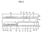
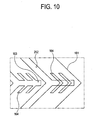
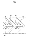
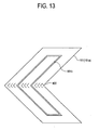
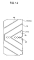
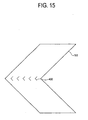
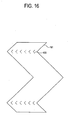
- Dispositif d'affichage à cristaux liquides comprenant :un premier substrat (100) comprenant une ligne de grille (121) et une ligne de données (141a, 141b), isolées l'une de l'autre et se croisant l'une l'autre,et une électrode de pixel (161, 161a, 161b) connectée à la ligne de grille (121) et à la ligne de données (141a, 141b) et comprenant un motif de découpage de l'électrode de pixel (162, 163),un deuxième substrat (200) disposé à l'opposé du premier substrat (100) et comprenant une électrode commune (251) avec un motif de découpage de l'électrode commune (252); etune couche de cristaux liquides (300) disposée entre le premier substrat (100) et le deuxième substrat (200),dans lequel l'électrode de pixel (161) comprend une première région et une deuxième région séparées l'une de l'autre dans une région frontière et s'étendant dans des directions différentes, etau moins une parmi l'électrode de pixel (161) et l'électrode commune (252) comprend un motif de découpage secondaire (164, 253) qui s'étend de la région frontière vers au moins une parmi la première région et la deuxième région,dans lequel le motif de découpage secondaire (164, 253) comprend une première partie (253a) s'étendant vers la première région et une deuxième partie (253b) s'étendant vers la deuxième région,dans lequel une direction d'extension de la première partie (253a) est sensiblement parallèle à la direction d'extension de la première région, et une direction d'extension de la deuxième partie (253b) est sensiblement parallèle à une direction d'extension de la deuxième région, l'électrode de pixel étant pliée le long d'une direction d'extension de la ligne de données dans la région frontière.
- Dispositif d'affichage à cristaux liquides selon la revendication 1, dans lequel un angle entre la direction d'extension de la première région et la ligne de grille (121) est plus grand qu'un angle entre une direction d'extension de la première partie et la ligne de grille (121), et
un angle entre une direction d'extension de la deuxième région et la ligne de grille (121) est plus grand qu'un angle entre une direction d'extension de la deuxième partie et la ligne de grille (121). - Dispositif d'affichage à cristaux liquides selon la revendication 1, dans lequel le motif de découpage secondaire (164, 253) a une forme en chevrons.
- Dispositif d'affichage à cristaux liquides selon la revendication 1, dans lequel un angle entre une direction d'extension de la première région et la ligne de grille (121) est d'environ 45°, et
la direction d'extension de la première région est sensiblement perpendiculaire à une direction d'extension de la deuxième région. - Dispositif d'affichage à cristaux liquides selon la revendication 1, dans lequel au moins une partie du motif de découpage secondaire (164) est reliée au motif de découpage de l'électrode de pixel (162, 163).
- Dispositif d'affichage à cristaux liquides selon la revendication 1, dans lequel au moins une partie du motif de découpage secondaire (253) est reliée au motif de découpage de l'électrode commune (252).
- Dispositif d'affichage à cristaux liquides selon la revendication 1, dans lequel le motif de découpage secondaire (164, 253) s'étend de 5 µm à 15 µm dans une direction d'extension de la ligne de données (141).
- Dispositif d'affichage à cristaux liquides selon la revendication 1, dans lequel au moins une parmi l'électrode de pixel (161) et l'électrode commune (251) comprend une pluralité de motifs de découpage secondaires (164, 253) disposés successivement le long d'une direction d'extension de la ligne de grille (121).
- Dispositif d'affichage à cristaux liquides selon la revendication 1, dans lequel la couche de cristaux liquides (300) est dans un mode d'alignement vertical.
- Dispositif d'affichage à cristaux liquides selon la revendication 1, dans lequel l'électrode de pixel (161) est pliée trois fois le long d'une direction d'extension de la ligne de données (121).
Applications Claiming Priority (1)
| Application Number | Priority Date | Filing Date | Title |
|---|---|---|---|
| KR1020070033731A KR101393634B1 (ko) | 2007-04-05 | 2007-04-05 | 액정표시장치 |
Publications (2)
| Publication Number | Publication Date |
|---|---|
| EP1978401A1 EP1978401A1 (fr) | 2008-10-08 |
| EP1978401B1 true EP1978401B1 (fr) | 2011-06-15 |
Family
ID=39415126
Family Applications (1)
| Application Number | Title | Priority Date | Filing Date |
|---|---|---|---|
| EP08005417A Active EP1978401B1 (fr) | 2007-04-05 | 2008-03-22 | Dispositif d'affichage à cristaux liquides |
Country Status (4)
| Country | Link |
|---|---|
| US (1) | US8081282B2 (fr) |
| EP (1) | EP1978401B1 (fr) |
| JP (1) | JP5260916B2 (fr) |
| KR (1) | KR101393634B1 (fr) |
Families Citing this family (6)
| Publication number | Priority date | Publication date | Assignee | Title |
|---|---|---|---|---|
| JP4828557B2 (ja) * | 2008-03-04 | 2011-11-30 | 株式会社 日立ディスプレイズ | 液晶表示装置 |
| KR101298424B1 (ko) * | 2008-12-08 | 2013-08-20 | 엘지디스플레이 주식회사 | 프린지 필드 스위칭 타입의 액정표시장치 |
| KR101668380B1 (ko) * | 2009-05-19 | 2016-10-24 | 삼성디스플레이 주식회사 | 액정 표시 장치 |
| EP2669882B1 (fr) * | 2012-05-31 | 2019-10-09 | Samsung Display Co., Ltd. | Dispositif d'affichage et procédé de commande associé |
| CN108806506A (zh) | 2017-05-05 | 2018-11-13 | 元太科技工业股份有限公司 | 开关元件阵列结构 |
| CN109285451B (zh) | 2017-07-21 | 2021-05-11 | 元太科技工业股份有限公司 | 像素数组基板 |
Family Cites Families (22)
| Publication number | Priority date | Publication date | Assignee | Title |
|---|---|---|---|---|
| US6977704B2 (en) | 2001-03-30 | 2005-12-20 | Fujitsu Display Technologies Corporation | Liquid crystal display |
| JP5041629B2 (ja) | 2001-06-06 | 2012-10-03 | 奇美電子股▲ふん▼有限公司 | 液晶表示装置 |
| JP4172750B2 (ja) | 2001-12-26 | 2008-10-29 | 東芝松下ディスプレイテクノロジー株式会社 | 液晶表示装置 |
| JP4076768B2 (ja) * | 2001-12-26 | 2008-04-16 | 東芝松下ディスプレイテクノロジー株式会社 | 液晶表示装置 |
| KR101337260B1 (ko) | 2003-08-13 | 2013-12-05 | 삼성디스플레이 주식회사 | 다중 도메인 액정 표시 장치 및 그 박막 트랜지스터 기판 |
| KR20050077571A (ko) | 2004-01-28 | 2005-08-03 | 삼성전자주식회사 | 다중 도메인 액정 표시 장치 |
| KR20050100959A (ko) | 2004-04-16 | 2005-10-20 | 삼성전자주식회사 | 어레이 기판 및 이의 제조 방법과, 이를 갖는 액정표시장치 |
| JP2005316331A (ja) | 2004-04-30 | 2005-11-10 | Toshiba Matsushita Display Technology Co Ltd | 液晶表示装置 |
| KR20060018401A (ko) | 2004-08-24 | 2006-03-02 | 삼성전자주식회사 | 다중 도메인 액정 표시 장치 |
| TWI261712B (en) | 2004-09-30 | 2006-09-11 | Chi Mei Optoelectronics Corp | Liquid crystal display |
| JP4604645B2 (ja) | 2004-10-22 | 2011-01-05 | セイコーエプソン株式会社 | 液晶表示装置及び電子機器 |
| JP4454487B2 (ja) | 2004-12-17 | 2010-04-21 | シャープ株式会社 | 液晶表示装置 |
| KR20060077896A (ko) | 2004-12-31 | 2006-07-05 | 엘지.필립스 엘시디 주식회사 | 멀티 도메인 액정 표시 장치 및 그 제조 방법 |
| JP4738000B2 (ja) * | 2005-01-19 | 2011-08-03 | シャープ株式会社 | 液晶表示装置 |
| KR101133761B1 (ko) * | 2005-01-26 | 2012-04-09 | 삼성전자주식회사 | 액정 표시 장치 |
| KR101137858B1 (ko) | 2005-03-16 | 2012-04-20 | 엘지디스플레이 주식회사 | 횡전계방식 액정표시소자 |
| KR20060111771A (ko) | 2005-04-25 | 2006-10-30 | 삼성전자주식회사 | 액정표시장치 |
| KR20060116580A (ko) | 2005-05-10 | 2006-11-15 | 삼성전자주식회사 | 액정 표시 장치 |
| TWI330735B (en) * | 2005-07-11 | 2010-09-21 | Chi Mei Optoelectronics Corp | Multi-domain vertical alignment lcd |
| KR101171180B1 (ko) * | 2005-07-15 | 2012-08-20 | 삼성전자주식회사 | 액정 표시 장치 |
| KR101230304B1 (ko) * | 2005-09-07 | 2013-02-06 | 삼성디스플레이 주식회사 | 액정 표시 장치 |
| KR20070035224A (ko) | 2005-09-27 | 2007-03-30 | 삼성전자주식회사 | 액정 표시 장치 |
-
2007
- 2007-04-05 KR KR1020070033731A patent/KR101393634B1/ko active IP Right Grant
- 2007-08-23 JP JP2007216619A patent/JP5260916B2/ja active Active
- 2007-12-04 US US11/950,304 patent/US8081282B2/en active Active
-
2008
- 2008-03-22 EP EP08005417A patent/EP1978401B1/fr active Active
Also Published As
| Publication number | Publication date |
|---|---|
| KR20080090649A (ko) | 2008-10-09 |
| US8081282B2 (en) | 2011-12-20 |
| JP5260916B2 (ja) | 2013-08-14 |
| JP2008257163A (ja) | 2008-10-23 |
| KR101393634B1 (ko) | 2014-05-12 |
| US20080246908A1 (en) | 2008-10-09 |
| EP1978401A1 (fr) | 2008-10-08 |
Similar Documents
| Publication | Publication Date | Title |
|---|---|---|
| US7349051B2 (en) | In plane switching mode liquid crystal display device having particular common lines | |
| JP4815584B2 (ja) | 液晶表示装置及びそれに使用される薄膜トランジスタ表示板 | |
| KR100730495B1 (ko) | 횡전계 방식의 액정표시장치 및 그 제조방법 | |
| US20040156005A1 (en) | Array substrate for in-plane switching mode liquid crystal display device and manufacturing method thereof | |
| US20070109479A1 (en) | In-plane switching mode liquid crystal display device and method of manufacturing the same | |
| US7688411B2 (en) | Multi-domain liquid crystal display device | |
| US7751009B2 (en) | Array substrate for in-plane switching mode liquid crystal display | |
| EP1978401B1 (fr) | Dispositif d'affichage à cristaux liquides | |
| KR20080030244A (ko) | 액정 표시 장치 | |
| US7929099B2 (en) | Liquid crystal display with improved lateral visibility | |
| US7804569B2 (en) | Panel assembly having a common electrode comprising a plurality of domain dividing members overlapping gate lines and wherein the gate lines overlap a pixel electrode | |
| US20080084528A1 (en) | Liquid crystal display device | |
| US9989814B2 (en) | Liquid crystal display | |
| KR20120130582A (ko) | 프린지 필드 스위칭 모드 액정표시장치용 어레이 기판 | |
| US8159642B2 (en) | In-plane switching mode liquid crystal display device having auxiliary pixel electrodes | |
| US10303008B2 (en) | Display device and mask for manufacturing display device | |
| KR101593007B1 (ko) | 프린지 필드 스위칭 모드 액정표시장치용 어레이 기판 | |
| KR101609826B1 (ko) | 프린지 필드 스위칭 모드 액정표시장치용 어레이 기판 | |
| KR20080024823A (ko) | 액정표시장치 | |
| KR20060062908A (ko) | 액정 표시 패널 | |
| KR20060020893A (ko) | 다중 도메인 박막 트랜지스터 표시판 | |
| KR101916868B1 (ko) | 액정표시장치용 어레이 기판 | |
| KR101905755B1 (ko) | 액정표시장치용 어레이 기판 | |
| KR20080070355A (ko) | 박막 트랜지스터 표시판 | |
| KR20090005863A (ko) | 액정 표시 장치 |
Legal Events
| Date | Code | Title | Description |
|---|---|---|---|
| PUAI | Public reference made under article 153(3) epc to a published international application that has entered the european phase |
Free format text: ORIGINAL CODE: 0009012 |
|
| AK | Designated contracting states |
Kind code of ref document: A1 Designated state(s): AT BE BG CH CY CZ DE DK EE ES FI FR GB GR HR HU IE IS IT LI LT LU LV MC MT NL NO PL PT RO SE SI SK TR |
|
| AX | Request for extension of the european patent |
Extension state: AL BA MK RS |
|
| 17P | Request for examination filed |
Effective date: 20090306 |
|
| 17Q | First examination report despatched |
Effective date: 20090403 |
|
| AKX | Designation fees paid |
Designated state(s): DE FR GB IT |
|
| GRAP | Despatch of communication of intention to grant a patent |
Free format text: ORIGINAL CODE: EPIDOSNIGR1 |
|
| GRAS | Grant fee paid |
Free format text: ORIGINAL CODE: EPIDOSNIGR3 |
|
| GRAA | (expected) grant |
Free format text: ORIGINAL CODE: 0009210 |
|
| AK | Designated contracting states |
Kind code of ref document: B1 Designated state(s): DE FR GB IT |
|
| REG | Reference to a national code |
Ref country code: GB Ref legal event code: FG4D |
|
| REG | Reference to a national code |
Ref country code: DE Ref legal event code: R096 Ref document number: 602008007525 Country of ref document: DE Effective date: 20110804 |
|
| PLBE | No opposition filed within time limit |
Free format text: ORIGINAL CODE: 0009261 |
|
| STAA | Information on the status of an ep patent application or granted ep patent |
Free format text: STATUS: NO OPPOSITION FILED WITHIN TIME LIMIT |
|
| 26N | No opposition filed |
Effective date: 20120316 |
|
| PG25 | Lapsed in a contracting state [announced via postgrant information from national office to epo] |
Ref country code: IT Free format text: LAPSE BECAUSE OF FAILURE TO SUBMIT A TRANSLATION OF THE DESCRIPTION OR TO PAY THE FEE WITHIN THE PRESCRIBED TIME-LIMIT Effective date: 20110615 |
|
| REG | Reference to a national code |
Ref country code: DE Ref legal event code: R097 Ref document number: 602008007525 Country of ref document: DE Effective date: 20120316 |
|
| REG | Reference to a national code |
Ref country code: DE Ref legal event code: R082 Ref document number: 602008007525 Country of ref document: DE Representative=s name: DR. WEITZEL & PARTNER, DE |
|
| REG | Reference to a national code |
Ref country code: DE Ref legal event code: R082 Ref document number: 602008007525 Country of ref document: DE Representative=s name: DR. WEITZEL & PARTNER, DE Effective date: 20130422 Ref country code: DE Ref legal event code: R081 Ref document number: 602008007525 Country of ref document: DE Owner name: INDUSTRIAL COOPERATION FOUNDATION OF CHONBUK N, KR Free format text: FORMER OWNER: INDUSTRIAL COOPERATION FOUNDATI, SAMSUNG ELECTRONICS CO., LTD., , KR Effective date: 20130422 Ref country code: DE Ref legal event code: R081 Ref document number: 602008007525 Country of ref document: DE Owner name: SAMSUNG DISPLAY CO., LTD., KR Free format text: FORMER OWNER: INDUSTRIAL COOPERATION FOUNDATI, SAMSUNG ELECTRONICS CO., LTD., , KR Effective date: 20130422 Ref country code: DE Ref legal event code: R082 Ref document number: 602008007525 Country of ref document: DE Representative=s name: DR. WEITZEL & PARTNER PATENT- UND RECHTSANWAEL, DE Effective date: 20130422 Ref country code: DE Ref legal event code: R081 Ref document number: 602008007525 Country of ref document: DE Owner name: SAMSUNG DISPLAY CO., LTD., YONGIN-CITY, KR Free format text: FORMER OWNER: INDUSTRIAL COOPERATION FOUNDATI, SAMSUNG ELECTRONICS CO., LTD., , KR Effective date: 20130422 Ref country code: DE Ref legal event code: R081 Ref document number: 602008007525 Country of ref document: DE Owner name: INDUSTRIAL COOPERATION FOUNDATION OF CHONBUK N, KR Free format text: FORMER OWNERS: INDUSTRIAL COOPERATION FOUNDATION OF CHONBUK NATIONAL UNIVERSITY, JEONJU-SI, KR; SAMSUNG ELECTRONICS CO., LTD., SUWON-SI, GYEONGGI-DO, KR Effective date: 20130422 Ref country code: DE Ref legal event code: R081 Ref document number: 602008007525 Country of ref document: DE Owner name: SAMSUNG DISPLAY CO., LTD., YONGIN-CITY, KR Free format text: FORMER OWNERS: INDUSTRIAL COOPERATION FOUNDATION OF CHONBUK NATIONAL UNIVERSITY, JEONJU-SI, KR; SAMSUNG ELECTRONICS CO., LTD., SUWON-SI, GYEONGGI-DO, KR Effective date: 20130422 |
|
| REG | Reference to a national code |
Ref country code: FR Ref legal event code: PLFP Year of fee payment: 9 |
|
| REG | Reference to a national code |
Ref country code: FR Ref legal event code: PLFP Year of fee payment: 10 |
|
| REG | Reference to a national code |
Ref country code: FR Ref legal event code: PLFP Year of fee payment: 11 |
|
| PGFP | Annual fee paid to national office [announced via postgrant information from national office to epo] |
Ref country code: FR Payment date: 20230221 Year of fee payment: 16 |
|
| P01 | Opt-out of the competence of the unified patent court (upc) registered |
Effective date: 20230530 |
|
| PGFP | Annual fee paid to national office [announced via postgrant information from national office to epo] |
Ref country code: DE Payment date: 20240220 Year of fee payment: 17 Ref country code: GB Payment date: 20240220 Year of fee payment: 17 |