EP1978401B1 - Flüssigkristallanzeigevorrichtung - Google Patents
Flüssigkristallanzeigevorrichtung Download PDFInfo
- Publication number
- EP1978401B1 EP1978401B1 EP08005417A EP08005417A EP1978401B1 EP 1978401 B1 EP1978401 B1 EP 1978401B1 EP 08005417 A EP08005417 A EP 08005417A EP 08005417 A EP08005417 A EP 08005417A EP 1978401 B1 EP1978401 B1 EP 1978401B1
- Authority
- EP
- European Patent Office
- Prior art keywords
- liquid crystal
- cutting pattern
- pixel electrode
- region
- extension direction
- Prior art date
- Legal status (The legal status is an assumption and is not a legal conclusion. Google has not performed a legal analysis and makes no representation as to the accuracy of the status listed.)
- Active
Links
- 239000004973 liquid crystal related substance Substances 0.000 title claims description 65
- 239000000758 substrate Substances 0.000 claims description 28
- 239000004576 sand Substances 0.000 claims 1
- 239000010410 layer Substances 0.000 description 64
- 239000010409 thin film Substances 0.000 description 19
- 230000005684 electric field Effects 0.000 description 13
- 239000012044 organic layer Substances 0.000 description 10
- 238000005452 bending Methods 0.000 description 9
- 230000002159 abnormal effect Effects 0.000 description 8
- 239000003990 capacitor Substances 0.000 description 8
- 238000002834 transmittance Methods 0.000 description 8
- 238000002161 passivation Methods 0.000 description 5
- 239000011159 matrix material Substances 0.000 description 4
- 239000004065 semiconductor Substances 0.000 description 4
- 108020001568 subdomains Proteins 0.000 description 3
- 229910052581 Si3N4 Inorganic materials 0.000 description 2
- 229910004205 SiNX Inorganic materials 0.000 description 2
- 229910021417 amorphous silicon Inorganic materials 0.000 description 2
- UMIVXZPTRXBADB-UHFFFAOYSA-N benzocyclobutene Chemical compound C1=CC=C2CCC2=C1 UMIVXZPTRXBADB-UHFFFAOYSA-N 0.000 description 2
- 239000004020 conductor Substances 0.000 description 2
- 238000010586 diagram Methods 0.000 description 2
- AMGQUBHHOARCQH-UHFFFAOYSA-N indium;oxotin Chemical compound [In].[Sn]=O AMGQUBHHOARCQH-UHFFFAOYSA-N 0.000 description 2
- 239000011810 insulating material Substances 0.000 description 2
- 229910052751 metal Inorganic materials 0.000 description 2
- 239000002184 metal Substances 0.000 description 2
- 239000011368 organic material Substances 0.000 description 2
- 239000000049 pigment Substances 0.000 description 2
- HQVNEWCFYHHQES-UHFFFAOYSA-N silicon nitride Chemical compound N12[Si]34N5[Si]62N3[Si]51N64 HQVNEWCFYHHQES-UHFFFAOYSA-N 0.000 description 2
- 239000002356 single layer Substances 0.000 description 2
- YVTHLONGBIQYBO-UHFFFAOYSA-N zinc indium(3+) oxygen(2-) Chemical compound [O--].[Zn++].[In+3] YVTHLONGBIQYBO-UHFFFAOYSA-N 0.000 description 2
- 239000004925 Acrylic resin Substances 0.000 description 1
- 229920000178 Acrylic resin Polymers 0.000 description 1
- YCKRFDGAMUMZLT-UHFFFAOYSA-N Fluorine atom Chemical compound [F] YCKRFDGAMUMZLT-UHFFFAOYSA-N 0.000 description 1
- 239000004642 Polyimide Substances 0.000 description 1
- GWEVSGVZZGPLCZ-UHFFFAOYSA-N Titan oxide Chemical compound O=[Ti]=O GWEVSGVZZGPLCZ-UHFFFAOYSA-N 0.000 description 1
- 150000001336 alkenes Chemical class 0.000 description 1
- 239000006229 carbon black Substances 0.000 description 1
- 239000011248 coating agent Substances 0.000 description 1
- 238000000576 coating method Methods 0.000 description 1
- 239000003086 colorant Substances 0.000 description 1
- 230000002542 deteriorative effect Effects 0.000 description 1
- 239000002019 doping agent Substances 0.000 description 1
- 230000000694 effects Effects 0.000 description 1
- 230000002708 enhancing effect Effects 0.000 description 1
- 229910052731 fluorine Inorganic materials 0.000 description 1
- 239000011737 fluorine Substances 0.000 description 1
- 230000001788 irregular Effects 0.000 description 1
- 238000000034 method Methods 0.000 description 1
- JRZJOMJEPLMPRA-UHFFFAOYSA-N olefin Natural products CCCCCCCC=C JRZJOMJEPLMPRA-UHFFFAOYSA-N 0.000 description 1
- 229910021420 polycrystalline silicon Inorganic materials 0.000 description 1
- 229920001721 polyimide Polymers 0.000 description 1
- 229920005591 polysilicon Polymers 0.000 description 1
- 239000011347 resin Substances 0.000 description 1
- 229920005989 resin Polymers 0.000 description 1
- 238000007650 screen-printing Methods 0.000 description 1
- 238000004528 spin coating Methods 0.000 description 1
- 238000006467 substitution reaction Methods 0.000 description 1
- OGIDPMRJRNCKJF-UHFFFAOYSA-N titanium oxide Inorganic materials [Ti]=O OGIDPMRJRNCKJF-UHFFFAOYSA-N 0.000 description 1
Images


Classifications
-
- G—PHYSICS
- G02—OPTICS
- G02F—OPTICAL DEVICES OR ARRANGEMENTS FOR THE CONTROL OF LIGHT BY MODIFICATION OF THE OPTICAL PROPERTIES OF THE MEDIA OF THE ELEMENTS INVOLVED THEREIN; NON-LINEAR OPTICS; FREQUENCY-CHANGING OF LIGHT; OPTICAL LOGIC ELEMENTS; OPTICAL ANALOGUE/DIGITAL CONVERTERS
- G02F1/00—Devices or arrangements for the control of the intensity, colour, phase, polarisation or direction of light arriving from an independent light source, e.g. switching, gating or modulating; Non-linear optics
- G02F1/01—Devices or arrangements for the control of the intensity, colour, phase, polarisation or direction of light arriving from an independent light source, e.g. switching, gating or modulating; Non-linear optics for the control of the intensity, phase, polarisation or colour
- G02F1/13—Devices or arrangements for the control of the intensity, colour, phase, polarisation or direction of light arriving from an independent light source, e.g. switching, gating or modulating; Non-linear optics for the control of the intensity, phase, polarisation or colour based on liquid crystals, e.g. single liquid crystal display cells
- G02F1/133—Constructional arrangements; Operation of liquid crystal cells; Circuit arrangements
- G02F1/1333—Constructional arrangements; Manufacturing methods
- G02F1/1343—Electrodes
- G02F1/134309—Electrodes characterised by their geometrical arrangement
-
- G—PHYSICS
- G02—OPTICS
- G02F—OPTICAL DEVICES OR ARRANGEMENTS FOR THE CONTROL OF LIGHT BY MODIFICATION OF THE OPTICAL PROPERTIES OF THE MEDIA OF THE ELEMENTS INVOLVED THEREIN; NON-LINEAR OPTICS; FREQUENCY-CHANGING OF LIGHT; OPTICAL LOGIC ELEMENTS; OPTICAL ANALOGUE/DIGITAL CONVERTERS
- G02F1/00—Devices or arrangements for the control of the intensity, colour, phase, polarisation or direction of light arriving from an independent light source, e.g. switching, gating or modulating; Non-linear optics
- G02F1/01—Devices or arrangements for the control of the intensity, colour, phase, polarisation or direction of light arriving from an independent light source, e.g. switching, gating or modulating; Non-linear optics for the control of the intensity, phase, polarisation or colour
- G02F1/13—Devices or arrangements for the control of the intensity, colour, phase, polarisation or direction of light arriving from an independent light source, e.g. switching, gating or modulating; Non-linear optics for the control of the intensity, phase, polarisation or colour based on liquid crystals, e.g. single liquid crystal display cells
- G02F1/133—Constructional arrangements; Operation of liquid crystal cells; Circuit arrangements
- G02F1/1333—Constructional arrangements; Manufacturing methods
- G02F1/1343—Electrodes
-
- G—PHYSICS
- G02—OPTICS
- G02F—OPTICAL DEVICES OR ARRANGEMENTS FOR THE CONTROL OF LIGHT BY MODIFICATION OF THE OPTICAL PROPERTIES OF THE MEDIA OF THE ELEMENTS INVOLVED THEREIN; NON-LINEAR OPTICS; FREQUENCY-CHANGING OF LIGHT; OPTICAL LOGIC ELEMENTS; OPTICAL ANALOGUE/DIGITAL CONVERTERS
- G02F1/00—Devices or arrangements for the control of the intensity, colour, phase, polarisation or direction of light arriving from an independent light source, e.g. switching, gating or modulating; Non-linear optics
- G02F1/01—Devices or arrangements for the control of the intensity, colour, phase, polarisation or direction of light arriving from an independent light source, e.g. switching, gating or modulating; Non-linear optics for the control of the intensity, phase, polarisation or colour
- G02F1/13—Devices or arrangements for the control of the intensity, colour, phase, polarisation or direction of light arriving from an independent light source, e.g. switching, gating or modulating; Non-linear optics for the control of the intensity, phase, polarisation or colour based on liquid crystals, e.g. single liquid crystal display cells
- G02F1/137—Devices or arrangements for the control of the intensity, colour, phase, polarisation or direction of light arriving from an independent light source, e.g. switching, gating or modulating; Non-linear optics for the control of the intensity, phase, polarisation or colour based on liquid crystals, e.g. single liquid crystal display cells characterised by the electro-optical or magneto-optical effect, e.g. field-induced phase transition, orientation effect, guest-host interaction or dynamic scattering
- G02F1/139—Devices or arrangements for the control of the intensity, colour, phase, polarisation or direction of light arriving from an independent light source, e.g. switching, gating or modulating; Non-linear optics for the control of the intensity, phase, polarisation or colour based on liquid crystals, e.g. single liquid crystal display cells characterised by the electro-optical or magneto-optical effect, e.g. field-induced phase transition, orientation effect, guest-host interaction or dynamic scattering based on orientation effects in which the liquid crystal remains transparent
- G02F1/1393—Devices or arrangements for the control of the intensity, colour, phase, polarisation or direction of light arriving from an independent light source, e.g. switching, gating or modulating; Non-linear optics for the control of the intensity, phase, polarisation or colour based on liquid crystals, e.g. single liquid crystal display cells characterised by the electro-optical or magneto-optical effect, e.g. field-induced phase transition, orientation effect, guest-host interaction or dynamic scattering based on orientation effects in which the liquid crystal remains transparent the birefringence of the liquid crystal being electrically controlled, e.g. ECB-, DAP-, HAN-, PI-LC cells
-
- G—PHYSICS
- G02—OPTICS
- G02F—OPTICAL DEVICES OR ARRANGEMENTS FOR THE CONTROL OF LIGHT BY MODIFICATION OF THE OPTICAL PROPERTIES OF THE MEDIA OF THE ELEMENTS INVOLVED THEREIN; NON-LINEAR OPTICS; FREQUENCY-CHANGING OF LIGHT; OPTICAL LOGIC ELEMENTS; OPTICAL ANALOGUE/DIGITAL CONVERTERS
- G02F1/00—Devices or arrangements for the control of the intensity, colour, phase, polarisation or direction of light arriving from an independent light source, e.g. switching, gating or modulating; Non-linear optics
- G02F1/01—Devices or arrangements for the control of the intensity, colour, phase, polarisation or direction of light arriving from an independent light source, e.g. switching, gating or modulating; Non-linear optics for the control of the intensity, phase, polarisation or colour
- G02F1/13—Devices or arrangements for the control of the intensity, colour, phase, polarisation or direction of light arriving from an independent light source, e.g. switching, gating or modulating; Non-linear optics for the control of the intensity, phase, polarisation or colour based on liquid crystals, e.g. single liquid crystal display cells
- G02F1/133—Constructional arrangements; Operation of liquid crystal cells; Circuit arrangements
- G02F1/1333—Constructional arrangements; Manufacturing methods
- G02F1/1337—Surface-induced orientation of the liquid crystal molecules, e.g. by alignment layers
- G02F1/13373—Disclination line; Reverse tilt
-
- G—PHYSICS
- G02—OPTICS
- G02F—OPTICAL DEVICES OR ARRANGEMENTS FOR THE CONTROL OF LIGHT BY MODIFICATION OF THE OPTICAL PROPERTIES OF THE MEDIA OF THE ELEMENTS INVOLVED THEREIN; NON-LINEAR OPTICS; FREQUENCY-CHANGING OF LIGHT; OPTICAL LOGIC ELEMENTS; OPTICAL ANALOGUE/DIGITAL CONVERTERS
- G02F1/00—Devices or arrangements for the control of the intensity, colour, phase, polarisation or direction of light arriving from an independent light source, e.g. switching, gating or modulating; Non-linear optics
- G02F1/01—Devices or arrangements for the control of the intensity, colour, phase, polarisation or direction of light arriving from an independent light source, e.g. switching, gating or modulating; Non-linear optics for the control of the intensity, phase, polarisation or colour
- G02F1/13—Devices or arrangements for the control of the intensity, colour, phase, polarisation or direction of light arriving from an independent light source, e.g. switching, gating or modulating; Non-linear optics for the control of the intensity, phase, polarisation or colour based on liquid crystals, e.g. single liquid crystal display cells
- G02F1/133—Constructional arrangements; Operation of liquid crystal cells; Circuit arrangements
- G02F1/1333—Constructional arrangements; Manufacturing methods
- G02F1/1343—Electrodes
- G02F1/134309—Electrodes characterised by their geometrical arrangement
- G02F1/134345—Subdivided pixels, e.g. for grey scale or redundancy
Definitions
- the present invention relates to a liquid crystal display device, and more specifically, to a liquid crystal display device having enhanced transmittance.
- a liquid crystal display (LCD) device in general, includes a first substrate with thin film transistors, a second substrate oppositely disposed to the first substrate, and a liquid crystal layer disposed between the first substrate and the second substrate.
- LCD liquid crystal display
- a patterned vertically aligned (PVA) mode and a multi-domain vertically aligned (MVA) mode have been developed.
- PVA mode and MVA mode a cutting pattern or a protrusion is provided on a pixel electrode and a common electrode. The cutting pattern or the protrusion adjusts the alignment of liquid crystal molecules in the liquid crystal layer due to an applied electric field, thereby enhancing the viewing angle.
- EP 1 762 884 A1 discloses a liquid crystal display including a substrate and a plurality of pixel electrodes that are formed on the substrate, each of the pixel electrodes including first and second subpixel electrodes.
- US 2003/0048401 A1 discloses a liquid crystal display based on a MVA mode of multi-division alignment.
- This invention provides a liquid crystal display device according to claim 1.
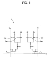
- FIG. 1 is an equivalent circuit diagram of one pixel in an LCD device according to a first exemplary embodiment of the present invention.
- a first thin film transistor T1 is connected to a first data line DL1 and a gate line GL
- a second thin film transistor T2 is connected to a second data line DL2 and the gate line GL
- the first thin film transistor T1 and the second thin film transistor T2 are connected to one gate line GL, and are thus driven simultaneously. However, the first thin film transistor T1 and the second thin film transistor T2 are connected to the first data line DL1 and the second data line DL2, respectively, and thus can receive different data voltages.
- a first liquid crystal capacitor C LC1 and a second liquid crystal capacitor C LC2 are connected to the first thin film transistor T1 and the second thin film transistor T2, respectively, and a first storage capacitor C st1 and a second storage capacitor C st2 are connected to the first thin film transistor T1 and the second thin film transistor T2, respectively.
- the first liquid crystal capacitor C LC1 and the second liquid crystal capacitor C LC2 are formed between a common electrode CE and a first pixel electrode PE1, and between the common electrode CE and a second pixel electrode PE2, respectively.
- the first storage capacitor C st1 and the second storage capacitor C st2 are formed between a storage capacitance line SL and the first pixel electrode PE1, and between the storage capacitance line SL and the second pixel electrode PE2, respectively.
- first pixel electrode PE1 and the second pixel electrode PE2 are separated from each other.
- the LCD device 1 may have improved visibility, which will be described below.
- the first pixel electrode PE1 receives a first data voltage from the first data line DL1 through the first thin film transistor T1.
- the second pixel electrode PE2 receives a second data voltage from the second data line DL2 through the second thin film transistor T2.
- the second data voltage may be different than the first data voltage. That is, one pixel includes two domains receiving different data voltages.
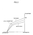
- FIG.2 illustrates a graph showing transmittance versus gradation in an LCD device according to an exemplary embodiment of the present invention.
- a domain having higher brightness may correspond to the first pixel electrode PE1
- a domain having lower brightness may correspond to the second pixel electrode PE2.
- two domains having different gamma curves may exist in one pixel, so that brightness and color viewed from the front and lateral sides of the LCD device may partially compensate for each other, thereby improving lateral visibility.
- the LCD device according to the first exemplary embodiment will now be described with reference to FIG. 3 , FIG. 4 , FIG. 5 , and FIG. 6 .
- FIG. 3 and FIG. 4 are plan views illustrating an LCD device according to a first exemplary embodiment of the present invention.
- FIG. 5 is a section view taken along line V-V in FIG. 3 of the LCD device according to the first exemplary embodiment of the present invention.
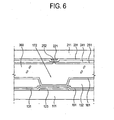
- FIG. 6 is a section view taken along line VI-VI in FIG. 3 of the LCD device according to the first exemplary embodiment of the present invention.
- a LCD device 1 includes a first substrate 100, a second substrate 200 opposite to the first substrate 100, and a liquid crystal layer 300 arranged between the first substrate 100 and the second substrate 200.
- the first substrate 100 will be described with reference to FIG. 3 and FIG. 5 .
- a gate wire which includes a gate line 121, a first gate electrode 122a, a second gate electrode 122b, and a storage capacitance line 123, is arranged on a first insulating substrate 111.
- the gate wire may include metal and be formed as a single layer or multiple layers.
- the gate line 121 extends transversely, the first gate electrode 122a and the second gate electrode 122b extend from the gate line 121, and the storage capacitance line 123 extends parallel with the gate line 121 and intersects a pixel.
- a gate insulating layer 131 including an insulating material such as silicon nitride (SiNx) is arranged on the first insulating substrate 111 and covers the gate wire.
- a semiconductor layer 132 may be made of amorphous silicon or polysilicon and is arranged on the gate insulating layer 131 in a region corresponding to the first gate electrode 122a .
- An ohmic contact layer 133 including n+ hydrogenated amorphous silicon highly doped with an n-type dopant is arranged on the semiconductor layer 132.
- the ohmic contact layer 133 is not included in a channel part between a first source electrode 142a and a first drain electrode 143a.
- a semiconductor layer (not shown) and an ohmic contact layer (not shown) are also arranged on the gate insulating layer 131 in a region corresponding to the second gate electrode 122b.
- a data wire including a first data line 141a and a second data line 141b, the first source electrode 142a, the second source electrode 142b, a first drain electrode 143a, and a second drain electrode 143b is arranged on the ohmic contact layer 133 and the gate insulating layer 131.
- the data wire may include metal and be formed as a single layer or multiple layers.
- the first thin film transistor T1 is connected to the first data line 141a, which may be arranged on the right side of the pixel, and the second thin film transistor T2 is connected to the second data line 141b, which may be arranged on the left side of the pixel.
- the first data line 141a and the second data line 141b may be bent but extend predominantly vertically as shown in FIG.
- the first source electrode 142a extends from the first data line 141a and extends to an upper part of the ohmic contact layer 133, and the first drain electrode 143a is separated from the first source electrode 142a and arranged on the ohmic contact layer 133 opposite to the first source electrode 142a.
- the second source electrode 142b extends from the second data line 141b and extends to an upper part of an ohmic contact layer (not shown), and the second drain electrode 143b is separated from the second source electrode 142b and arranged on the ohmic contact layer (not shown) opposite to the second source electrode 142b.
- the first gate electrode 122a, the first source electrode 142a, and the first drain electrode 143a are elements of the first thin film transistor T1.
- the second gate electrode 122b, the second source electrode 142b, and the second drain electrode 143b are elements of the second thin film transistor T2.
- a passivation layer 151 including an insulating material such as silicon nitride (SiNx) is arranged on the data wire and exposed portions of the semiconductor layer 132 not covered by the data wire.
- An organic layer 152 is arranged on the passivation layer 151.
- the organic layer 152 may be thicker than the gate insulating layer 131 and the passivation layer 151.
- the organic layer 152 may be formed by a method such as spin coating, slit coating, or screen printing.
- the organic layer 152 may be one of benzocyclobutene (BCB) series, olefin series, acrylic resin series, polyimide series, and fluorine resin.
- BCB benzocyclobutene
- a first contact hole 171a, a second contact hole 171b, and an opening 172 as shown in FIG. 6 are arranged in the organic layer 152.
- the first contact hole 171a and the second contact hole 171b are also arranged in the passivation layer 151, and expose the first drain electrode 143a and the second drain electrode 143b, respectively.
- the opening 172 corresponds to the storage capacitance line 123 and exposes the passivation layer 151.
- the organic layer 152 is not arranged in the opening 172.
- the pixel electrode 161 is arranged on the organic layer 152.
- the pixel electrode 161 may include a transparent conductive material such as indium tin oxide (ITO) or indium zinc oxide (IZO).
- the pixel electrode 161 extends along the extension direction of the first data line 141a and the second data line 141b and may be bent three times.
- the pixel electrode 161 may have a structure symmetrical about a horizontal line.
- the storage capacitance line 123 crosses with a bending part of the pixel electrode 161.
- the pixel electrode 161 includes a first pixel electrode 161a and a second pixel electrode 161b separated from each other by a first pixel electrode cutting pattern 162.
- the second pixel electrode 161b may have a chevron shape according to the bent shape of the pixel electrode 161, and is positioned in a center region of the pixel.
- the first pixel electrode 161a may surround the second pixel electrode 161b, and the area of the first pixel electrode 161a may be larger than the area of the second pixel electrode 161b.
- the first pixel electrode 161a is connected to the drain electrode 143a of the first thin film transistor T1 through the first contact hole 171a.
- the second pixel electrode 161b is connected to the drain electrode 143b of the second thin film transistor T2 through the second contact hole 171b.
- the pixel electrode 161 is arranged closer to the storage capacitance line 123 through the opening 172 since the organic layer 152 is not arranged between the pixel electrode 161 and the storage capacitance line 123 in the opening 172.
- a storage capacitance Cst is formed between the pixel electrode 161 receiving a pixel voltage and the storage capacitance line 123 receiving a common voltage.
- the organic layer 152 is removed in the opening 172 because the organic layer 152 may be too thick and may have permittivity that is too low to form the storage capacitance Cst between the pixel electrode 161 and the storage capacitance line 123.
- the storage capacitance line 123 overlaps more with the first pixel electrode 161a than with the second pixel electrode 161b because the domain corresponding to the larger first pixel electrode 161a may use a higher storage capacitance Cst.
- a second pixel electrode cutting pattern 163 is arranged in both the first pixel electrode 161a and the second pixel electrode 161b. A part of the second pixel electrode cutting pattern 163 extends parallel with portions of the first data line 141a and the second data line 141b, and another part of the second pixel electrode cutting pattern 163 extends parallel with the gate line 121.
- the sub domains are surrounded by the first pixel electrode cutting pattern 162 or an edge of the pixel electrode 161, the second pixel electrode cutting pattern 163, and the common electrode cutting pattern 252, and extend in an oblique direction.
- a hatched area indicates a first sub domain and a dotted area indicates a second sub domain within a domain.
- the first sub domain and the second sub domain neighbor each other in the extension direction of the first data line 141a and the second data line 141b. Further, the first sub domain and the second sub domain extend at an approximately right angle to each other.
- first sub cutting patterns 164 are arranged in upper and lower regions of the bending part of the pixel electrode 161.
- the first sub cutting pattern 164 is connected to the first pixel electrode cutting pattern 162 and the second pixel electrode cutting pattern 163, and extends in the extension direction of the first data line 141a and the second data line 141b.
- the second substrate 200 will be described with reference to FIG. 4 and FIG. 5 .
- FIG. 4 illustrates an arrangement between a pixel electrode 161 of the first substrate 100 and a common electrode cutting pattern 252 of the second substrate 200.
- a black matrix 221 is arranged on a second insulating substrate 211.
- the black matrix 221 may include a photosensitive organic material with a black pigment.
- the black pigment may include carbon black or titanium oxide.
- a color filter layer 231 is arranged on the second insulating layer 211 and the black matrix 221.
- the color filter layer 231 may include sub layers with different colors, such as red sub layers, green sub layers, and blue sub layers, each corresponding to a pixel.
- the color filter layer 231 may be continuous in a region corresponding to the black matrix 221 between adjacent pixels as shown in FIG. 5 and FIG. 8 , or may be discontinuous (not shown).
- An overcoat layer 241 may be arranged on the color filter layer 231 to planarize the second substrate 200.
- the common electrode 251 is arranged on the overcoat layer 241.
- the common electrode 251 includes a transparent conductive material such as indium tin oxide (ITO) or indium zinc oxide (IZO).
- ITO indium tin oxide
- IZO indium zinc oxide
- the common electrode 251 receives a common voltage, and the potential difference between the common electrode 251 and the pixel electrode 161 of the first substrate 100 generates an electric field across the liquid crystal layer 300.
- a common electrode cutting pattern 252 is arranged in the common electrode 251. As shown in FIG. 4 , a part of the common electrode cutting pattern 252 extends parallel with the first pixel electrode cutting pattern 162, and another part of the common electrode cutting pattern 252 extends parallel with the gate line 121.
- a second sub cutting pattern 253 connected to the common electrode cutting pattern 252 is arranged corresponding to upper regions and lower regions of the bending part in the pixel electrode 161.
- the second sub cutting pattern 253 extends parallel with the first data line 141a and the second data line 141b.
- the arrangements of the first pixel electrode cutting pattern 162, the second pixel electrode cutting pattern 163, and the common electrode cutting pattern 252 are not limited to those in the first exemplary embodiment.
- the first pixel electrode cutting pattern 162, the second pixel electrode cutting pattern 163, and the common electrode cutting pattern 252 may be formed in various shapes, including those shapes and arrangements disclosed below.
- the liquid crystal layer 300 is disposed between the first substrate 100 and the second substrate 200.
- the liquid crystal layer 300 is in a vertically aligned (VA) mode, in which long axes of liquid crystal molecules are vertically aligned when an electric field is not generated across the liquid crystal layer 300.
- VA vertically aligned
- the liquid crystal molecules When receiving a voltage, the liquid crystal molecules are aligned perpendicularly to an applied electric field due to negative dielectric anisotropy. If the first pixel electrode cutting pattern 162, the second pixel electrode cutting pattern 163, and the common electrode cutting pattern 252 are not included in the LCD device 1, the liquid crystal molecules may be oriented in irregular directions where the electric fields are disrupted, thereby forming a disclination line along a boundary between the liquid crystal molecules having disrupted orientations. The first pixel electrode cutting pattern 162, the second pixel electrode cutting pattern 163, and the common electrode cutting pattern 252 form a fringe electric field and determine the lying direction of the liquid crystal alignment when an electric field is generated across the liquid crystal layer 300.
- An aperture ratio of the LCD device 1 is improved by first sub cutting pattern 164 and the second sub cutting pattern 253.
- the aperture ratio improvement will be described with reference to the second sub cutting pattern 253 arranged in the common electrode 251 in FIG. 7 by way of example.
- a first sub domain is elongated in the first direction and a second sub domain is elongated in the second direction.
- the first direction is perpendicular to the second direction, and the angle ⁇ 1 between the first direction and the gate line 121 is about 45°.
- a bending region which may be referred to as a boundary region, is arranged between the first sub domain and the second sub domain.
- the second sub cutting pattern 253 includes a first part 253a extending from the bending region (the boundary region) to the first sub domain, and a second part 253b extending from the bending region to the second sub domain.
- the first part 253a and the second part 253b extend in parallel with the first direction of the first sub domain and the second direction of the second sub domain, respectively.
- the angel ⁇ 2 between the first part 253a and the gate line 121 is about 45°
- the extension direction of the first part 253a is perpendicular to the extension direction of the second part 253b.
- a liquid crystal director of a liquid crystal layer 300 in the first sub domain is aligned almost in parallel with the first direction, and the liquid crystal director of the liquid crystal layer 300 in the second sub domain is aligned almost in parallel with the second direction.
- liquid crystal directors are perpendicular to and collide with each other in the boundary region where the first sub domain meets the second sub domain.
- the liquid crystal layer 300 is divided into a normal liquid crystal layer 300a having the liquid crystal directors aligned in the first direction or the second direction, and an abnormal liquid crystal layer 300b having the liquid crystal directors aligned in a direction different than the first direction or the second direction.
- the abnormal liquid crystal layer 300b has the liquid crystal director approximately perpendicular to the gate line 121 in the boundary region.
- the abnormal liquid crystal layer 300b includes more randomly oriented liquid crystals, which may cause the disclination line, thereby deteriorating a display quality.
- the liquid crystal layer 300 has the highest transmittance when the liquid crystal directors are aligned at an angle of 45° to a horizontal direction (if one of a pair of polarizing axes is horizontal and the other polarizing axis is vertical). However, if the angle of the liquid crystal director of the abnormal liquid crystal 300b is larger than 45°, the transmittance may deteriorate.
- the second sub cutting pattern 253 forms an additional electric field in the vicinity of the boundary region and minimizes the region having the abnormal liquid crystal layer 300b. By this, a width d1 of the disclination region B is reduced and the transmittance is thus improved.
- the width of the disclination region may be 10 ⁇ m.
- a length d2 of the second sub cutting pattern 253 may be 5 ⁇ m to 15 ⁇ m.
- An interval d3 between the second sub cutting patterns 253 may be 5.5 ⁇ m to 7.6 ⁇ m, and a width d4 of the second sub cutting pattern 253 may be 3 ⁇ m to 5 ⁇ m, but these dimensions are not limited thereto.
- An interval d5 between the first sub cutting patterns 164 may be 100 percent to 130 percent of the interval d3 between the second sub cutting patterns 253, and a width d6 of the first sub cutting pattern 164 may be 70 percent to 100 percent of the width d4 of the second sub cutting pattern 164, but these dimensions are not limited thereto.
- the first pixel electrode cutting pattern 162, the second pixel electrode cutting pattern 163, the common electrode cutting pattern 252 and the first sub cutting pattern 164 and the second sub cutting pattern 253 are used as domain dividers for dividing the liquid crystal layer 300 into domains.
- the domain dividers are not limited to the cutting pattern of the first exemplary embodiment, which has been described.
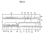
- FIG. 8 illustrates a section view of an LCD device according to a second exemplary embodiment of the present invention. More specifically, FIG. 8 is a section view corresponding to line V-V in FIG. 3 of an LCD device according to a second exemplary embodiment of the present invention. The second exemplary embodiment will be described with reference to FIG. 8 .
- the common electrode 251 is not patterned and a protrusion 255 is arranged in a position corresponding to the common electrode cutting pattern 252 of the first exemplary embodiment.
- the protrusion 255 may be made of an organic material and, together with the first pixel electrode cutting pattern 162 and the second pixel electrode cutting pattern 163, divides the liquid crystal layer 300 into sub domains like the common electrode cutting pattern 252.
- a sub protrusion (not shown) may be arranged on the common electrode 251 instead of the second sub cutting pattern 253 of the first exemplary embodiment.
- a sub protrusion may be arranged in a position corresponding to the first sub cutting pattern 164 of the first exemplary embodiment.
- FIG. 9 illustrates a plan view of an LCD device according to a third exemplary embodiment of the present invention. More specifically, FIG. 9 is a plan view corresponding to region A in FIG. 4 of an LCD device according to a third exemplary embodiment of the present invention. The third exemplary embodiment will be described with reference to FIG. 9 .
- the first sub cutting patterns 164 are arranged to alternate with the second sub cutting patterns 253 such that a second sub cutting pattern 253 is arranged between first sub cutting patterns 164, and a first sub cutting pattern 164 is arranged between second sub cutting patterns 253.
- the first sub cutting patterns 164 and the second sub cutting patterns 253 are densely arranged so that the width of the disclination region B having the abnormal liquid crystal layer 300b can be further reduced.
- first sub cutting pattern 164 and the second sub cutting pattern 253 may partially or completely overlap each other.
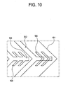
- FIG. 10 illustrates a plan view of an LCD device according to a fourth exemplary embodiment of the present invention. More specifically, FIG. 10 is a plan view corresponding to region A in FIG. 4 of an LCD device according to a fourth exemplary embodiment of the present invention. The fourth exemplary embodiment will be described with reference to FIG. 10 .
- a common electrode 251 according to a fourth exemplary embodiment of the present invention includes the common electrode cutting pattern 252, but does not include the second sub cutting pattern 253.
- a first sub cutting pattern 164 is provided in a position corresponding to the second sub cutting pattern253 of the first exemplary embodiment.
- the first sub cutting pattern 164 may not be arranged in the pixel electrode 161, and the second sub cutting pattern 253 may be arranged in the common electrode 251.
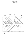
- FIG. 11 illustrates a plan view of an LCD device according to a fifth exemplary embodiment of the present invention. More specifically, FIG. 11 is a plan view corresponding to region A in FIG. 4 of an LCD device according to a fifth exemplary embodiment of the present invention. The fifth exemplary embodiment will be described with reference to FIG. 11 .
- a first sub cutting pattern 164 is separated from a second pixel electrode cutting pattern 163, and a second sub cutting pattern 253 is separated from a common electrode cutting pattern 252.
- FIG. 12 illustrates a plan view of an LCD device according to a sixth exemplary embodiment of the present invention. More specifically, FIG. 12 is a plan view corresponding to region A in FIG. 4 of an LCD device according to a sixth exemplary embodiment of the present invention. The sixth exemplary embodiment will be described with reference to FIG. 12 .
- an angle between a second sub cutting pattern 253 and a gate line 121 is relatively small. More specifically, an angle ⁇ 3 between a second sub cutting pattern 253 and a gate line 121 is less than 45°. The angle ⁇ 3 between the second sub cutting pattern 253 and the gate line 121 may be 25° to 40°.
- an electric field formed across sub cutting patterns 164 and 253 has an increased effect on the liquid crystal director of an abnormal liquid crystal layer 300b, thereby further reducing the width of the disclination region B having the abnormal liquid crystal layer 300b.
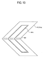
- FIG. 13 illustrates a plan view of an LCD device according to a seventh exemplary embodiment of the present invention. More specifically, FIG. 13 is a plan view corresponding to region A in FIG. 4 of an LCD device according to a seventh exemplary embodiment of the present invention. The seventh exemplary embodiment will be described with reference to FIG. 13 .
- Pixel electrodes 161 have a chevron shape, and are bent once along the extension direction of a first data line 141a and/or a second data line 141b.
- the pixel electrode 161 includes a first pixel electrode 161a and a second pixel electrode 161b, which are separated from each other.
- a sub cutting pattern 400 is arranged in a bending part along an extension direction of the gate line 121, and the sub cutting pattern 400 may extend in a direction of a first data line 141a and/or a second data line 141b.
- the sub cutting pattern 400 may be arranged in the pixel electrode 161 and/or the common electrode 251.
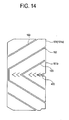
- FIG. 14 illustrates a plan view of an LCD device according to an eighth exemplary embodiment of the present invention. More specifically, FIG. 14 is a plan view corresponding to region A in FIG. 4 of an LCD device according to an eighth exemplary embodiment of the present invention. The eighth exemplary embodiment will be described with respect to FIG. 14 .
- Pixel electrodes 161 have an approximately rectangular shape, and include a first pixel electrode 161a and a second pixel electrode 161b, which are separated from each other.
- the pixel electrodes 161 have generally rectangular shape, but have a region where the electric fields collide with each other in the first pixel electrode cutting pattern 162 and the second pixel electrode cutting pattern 163.
- a sub cutting pattern 400 is arranged in the region where the electric fields collide with each other.
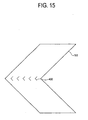
- FIG. 15 illustrates a plan view of an LCD device according to a ninth exemplary embodiment of the present invention. More specifically, FIG. 15 is a plan view corresponding to region A in FIG. 4 of an LCD device according to a ninth exemplary embodiment of the present invention. The ninth exemplary embodiment will be described with reference to FIG. 15 .
- a pixel electrode 161 has a chevron shape and is bent once along an extension direction of a first data line 141a and/or a second data line 141b. Although a cutting pattern is not shown, the pixel electrode 161 is wholly connected.
- a sub cutting pattern 400 is arranged in a bending part along an extension direction of the gate line 121, and the sub cutting pattern 400 may extend in a direction of a first data line 141a and/or a second data line 141b.
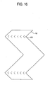
- FIG. 16 illustrates a plan view of an LCD device according to a tenth exemplary embodiment of the present invention. More specifically, FIG. 16 is a plan view corresponding to region A in FIG. 4 of an LCD device according to a tenth exemplary embodiment of the present invention. The tenth exemplary embodiment will be described with reference to FIG. 16 .
- a pixel electrode 161 is bent three times along an extension direction of a first data line 141a and/or a second data line 141b. Although a cutting pattern is not shown, the pixel electrode 161 is wholly connected.
- a sub cutting pattern 400 is arranged in a bending part along an extension direction of the gate line 121, and the sub cutting pattern 400 may extend in a direction of a first data line 141a and/or a second data line 141b.
- the present invention provides an LCD device which has an enhanced transmittance.
Claims (10)
- Flüssigkristalldisplayvorrichtung, umfassend:ein erstes Substrat (100), das eine Gate-Leitung (121) und eine Datenleitung (141a, 141b) umfasst, die voneinander isoliert sind und einander kreuzen, sowie eine Pixelelektrode (161, 161a, 161b), die mit der Gate-Leitung (121) und der Datenleitung (141a, 141b) verbunden ist und ein Pixelelektrodenschnittmuster (162, 163) umfasst;ein zweites Substrat (200), das gegenüber dem ersten Substrat (100) angeordnet ist und eine gemeinsame Elektrode (251) umfasst, die ein gemeinsames Elektrodenschnittmuster (252) umfasst; undeine Flüssigkristallschicht (300), die zwischen dem ersten Substrat (100) und dem zweiten Substrat (200) angeordnet ist;wobei die Pixelelektrode (161) einen ersten Bereich und einen zweiten Bereich umfasst, die voneinander in einem Randbereich getrennt sind und sich in unterschiedliche Richtungen erstrecken; undwobei die Pixelelektrode (161) und/oder die gemeinsame Elektrode (252) ein Teilschnittmuster (164, 253) umfasst, das sich von dem Randbereich zu dem ersten Bereich und/oder dem zweiten Bereich erstreckt;wobei das Teilschnittmuster (164, 253) einen ersten Teil (253a), der sich zu dem ersten Bereich erstreckt, und einen zweiten Teil (253b), der sich zu dem zweiten Bereich erstreckt, umfasst;wobei eine Erstreckungsrichtung des ersten Teils (253a) im wesentlichen parallel zu einer Erstreckungsrichtung des ersten Bereichs ist, undeine Erstreckungsrichtung des zweiten Teils (253b) im wesentlichen parallel zu einer Erstreckungsrichtung des zweiten Bereichs ist,wobei die Pixelelektrode in einer Erstreckungsrichtung der Datenleitung an dem Randbereich gebogen ist.
- Flüssigkristalldisplayvorrichtung gemäß Anspruch 1, wobei ein Winkel zwischen einer Erstreckungsrichtung des ersten Bereichs und der Gate-Leitung (121) größer ist als ein Winkel zwischen einer Erstreckungsrichtung des ersten Teils und der Gate-Leitung (121), und
ein Winkel zwischen einer Erstreckungsrichtung des zweiten Bereichs und der Gate-Leitung (121) größer ist als ein Winkel zwischen einer Erstreckungsrichtung des zweiten Teils und der Gate-Leitung (121). - Flüssigkristalldisplayvorrichtung gemäß Anspruch 1, wobei das Teilschnittmuster (164, 253) eine Chevron-Form aufweist.
- Flüssigkristalldisplayvorrichtung gemäß Anspruch 1, wobei ein Winkel zwischen einer Erstreckungsrichtung des ersten Bereichs und der Gate-Leitung (121) etwa 45° ist, und
die Erstreckungsrichtung des ersten Bereichs im wesentlichen rechtwinkelig zu einer Erstreckungsrichtung des zweiten Bereichs ist. - Flüssigkristalldisplayvorrichtung gemäß Anspruch 1, wobei mindestens ein Teil des Teilschnittmusters (164) mit dem Schnittmuster der Pixelelektroden (162, 163) verbunden ist.
- Flüssigkristalldisplayvorrichtung gemäß Anspruch 1, wobei mindestens ein Teil des Teilschnittmusters (253) mit dem Schnittmuster (252) der gemeinsamen Elektrode verbunden ist.
- Flüssigkristalldisplayvorrichtung gemäß Anspruch 1, wobei sich das Teilschnittmuster (164, 253) 5 µm bis 15 µm in einer Erstreckungsrichtung der Datenleitung (141) erstreckt.
- Flüssigkristalldisplayvorrichtung gemäß Anspruch 1, wobei die Pixelelektrode (161) und/oder die gemeinsamer Elektrode (251) eine Mehrzahl von Teilschnittmustern (164, 253) umfasst, die aufeinander folgend in einer Erstreckungsrichtung der Gate-Leitung (121) angeordnet sind.
- Flüssigkristalldisplayvorrichtung gemäß Anspruch 1, wobei die Flüssigkristallschicht (300) einen vertikal ausgerichteten Modus aufweist.
- Flüssigkristalldisplayvorrichtung gemäß Anspruch 1, wobei die Pixelelektrode (161) dreimal in einer Erstreckungsrichtung der Datenleitung (121) gebogen ist.
Applications Claiming Priority (1)
| Application Number | Priority Date | Filing Date | Title |
|---|---|---|---|
| KR1020070033731A KR101393634B1 (ko) | 2007-04-05 | 2007-04-05 | 액정표시장치 |
Publications (2)
| Publication Number | Publication Date |
|---|---|
| EP1978401A1 EP1978401A1 (de) | 2008-10-08 |
| EP1978401B1 true EP1978401B1 (de) | 2011-06-15 |
Family
ID=39415126
Family Applications (1)
| Application Number | Title | Priority Date | Filing Date |
|---|---|---|---|
| EP08005417A Active EP1978401B1 (de) | 2007-04-05 | 2008-03-22 | Flüssigkristallanzeigevorrichtung |
Country Status (4)
| Country | Link |
|---|---|
| US (1) | US8081282B2 (de) |
| EP (1) | EP1978401B1 (de) |
| JP (1) | JP5260916B2 (de) |
| KR (1) | KR101393634B1 (de) |
Families Citing this family (6)
| Publication number | Priority date | Publication date | Assignee | Title |
|---|---|---|---|---|
| JP4828557B2 (ja) * | 2008-03-04 | 2011-11-30 | 株式会社 日立ディスプレイズ | 液晶表示装置 |
| KR101298424B1 (ko) * | 2008-12-08 | 2013-08-20 | 엘지디스플레이 주식회사 | 프린지 필드 스위칭 타입의 액정표시장치 |
| KR101668380B1 (ko) * | 2009-05-19 | 2016-10-24 | 삼성디스플레이 주식회사 | 액정 표시 장치 |
| EP2669882B1 (de) * | 2012-05-31 | 2019-10-09 | Samsung Display Co., Ltd. | Anzeigevorrichtung und Verfahren dafür |
| CN108806506A (zh) | 2017-05-05 | 2018-11-13 | 元太科技工业股份有限公司 | 开关元件阵列结构 |
| CN109285451B (zh) | 2017-07-21 | 2021-05-11 | 元太科技工业股份有限公司 | 像素数组基板 |
Family Cites Families (22)
| Publication number | Priority date | Publication date | Assignee | Title |
|---|---|---|---|---|
| US6977704B2 (en) | 2001-03-30 | 2005-12-20 | Fujitsu Display Technologies Corporation | Liquid crystal display |
| JP5041629B2 (ja) | 2001-06-06 | 2012-10-03 | 奇美電子股▲ふん▼有限公司 | 液晶表示装置 |
| JP4172750B2 (ja) | 2001-12-26 | 2008-10-29 | 東芝松下ディスプレイテクノロジー株式会社 | 液晶表示装置 |
| JP4076768B2 (ja) * | 2001-12-26 | 2008-04-16 | 東芝松下ディスプレイテクノロジー株式会社 | 液晶表示装置 |
| KR101337260B1 (ko) | 2003-08-13 | 2013-12-05 | 삼성디스플레이 주식회사 | 다중 도메인 액정 표시 장치 및 그 박막 트랜지스터 기판 |
| KR20050077571A (ko) | 2004-01-28 | 2005-08-03 | 삼성전자주식회사 | 다중 도메인 액정 표시 장치 |
| KR20050100959A (ko) | 2004-04-16 | 2005-10-20 | 삼성전자주식회사 | 어레이 기판 및 이의 제조 방법과, 이를 갖는 액정표시장치 |
| JP2005316331A (ja) | 2004-04-30 | 2005-11-10 | Toshiba Matsushita Display Technology Co Ltd | 液晶表示装置 |
| KR20060018401A (ko) | 2004-08-24 | 2006-03-02 | 삼성전자주식회사 | 다중 도메인 액정 표시 장치 |
| TWI261712B (en) | 2004-09-30 | 2006-09-11 | Chi Mei Optoelectronics Corp | Liquid crystal display |
| JP4604645B2 (ja) | 2004-10-22 | 2011-01-05 | セイコーエプソン株式会社 | 液晶表示装置及び電子機器 |
| JP4454487B2 (ja) | 2004-12-17 | 2010-04-21 | シャープ株式会社 | 液晶表示装置 |
| KR20060077896A (ko) | 2004-12-31 | 2006-07-05 | 엘지.필립스 엘시디 주식회사 | 멀티 도메인 액정 표시 장치 및 그 제조 방법 |
| JP4738000B2 (ja) * | 2005-01-19 | 2011-08-03 | シャープ株式会社 | 液晶表示装置 |
| KR101133761B1 (ko) * | 2005-01-26 | 2012-04-09 | 삼성전자주식회사 | 액정 표시 장치 |
| KR101137858B1 (ko) | 2005-03-16 | 2012-04-20 | 엘지디스플레이 주식회사 | 횡전계방식 액정표시소자 |
| KR20060111771A (ko) | 2005-04-25 | 2006-10-30 | 삼성전자주식회사 | 액정표시장치 |
| KR20060116580A (ko) | 2005-05-10 | 2006-11-15 | 삼성전자주식회사 | 액정 표시 장치 |
| TWI330735B (en) * | 2005-07-11 | 2010-09-21 | Chi Mei Optoelectronics Corp | Multi-domain vertical alignment lcd |
| KR101171180B1 (ko) * | 2005-07-15 | 2012-08-20 | 삼성전자주식회사 | 액정 표시 장치 |
| KR101230304B1 (ko) * | 2005-09-07 | 2013-02-06 | 삼성디스플레이 주식회사 | 액정 표시 장치 |
| KR20070035224A (ko) | 2005-09-27 | 2007-03-30 | 삼성전자주식회사 | 액정 표시 장치 |
-
2007
- 2007-04-05 KR KR1020070033731A patent/KR101393634B1/ko active IP Right Grant
- 2007-08-23 JP JP2007216619A patent/JP5260916B2/ja active Active
- 2007-12-04 US US11/950,304 patent/US8081282B2/en active Active
-
2008
- 2008-03-22 EP EP08005417A patent/EP1978401B1/de active Active
Also Published As
| Publication number | Publication date |
|---|---|
| KR20080090649A (ko) | 2008-10-09 |
| US8081282B2 (en) | 2011-12-20 |
| JP5260916B2 (ja) | 2013-08-14 |
| JP2008257163A (ja) | 2008-10-23 |
| KR101393634B1 (ko) | 2014-05-12 |
| US20080246908A1 (en) | 2008-10-09 |
| EP1978401A1 (de) | 2008-10-08 |
Similar Documents
| Publication | Publication Date | Title |
|---|---|---|
| US7349051B2 (en) | In plane switching mode liquid crystal display device having particular common lines | |
| JP4815584B2 (ja) | 液晶表示装置及びそれに使用される薄膜トランジスタ表示板 | |
| KR100730495B1 (ko) | 횡전계 방식의 액정표시장치 및 그 제조방법 | |
| US20040156005A1 (en) | Array substrate for in-plane switching mode liquid crystal display device and manufacturing method thereof | |
| US20070109479A1 (en) | In-plane switching mode liquid crystal display device and method of manufacturing the same | |
| US7688411B2 (en) | Multi-domain liquid crystal display device | |
| US7751009B2 (en) | Array substrate for in-plane switching mode liquid crystal display | |
| EP1978401B1 (de) | Flüssigkristallanzeigevorrichtung | |
| KR20080030244A (ko) | 액정 표시 장치 | |
| US7929099B2 (en) | Liquid crystal display with improved lateral visibility | |
| US7804569B2 (en) | Panel assembly having a common electrode comprising a plurality of domain dividing members overlapping gate lines and wherein the gate lines overlap a pixel electrode | |
| US20080084528A1 (en) | Liquid crystal display device | |
| US9989814B2 (en) | Liquid crystal display | |
| KR20120130582A (ko) | 프린지 필드 스위칭 모드 액정표시장치용 어레이 기판 | |
| US8159642B2 (en) | In-plane switching mode liquid crystal display device having auxiliary pixel electrodes | |
| US10303008B2 (en) | Display device and mask for manufacturing display device | |
| KR101593007B1 (ko) | 프린지 필드 스위칭 모드 액정표시장치용 어레이 기판 | |
| KR101609826B1 (ko) | 프린지 필드 스위칭 모드 액정표시장치용 어레이 기판 | |
| KR20080024823A (ko) | 액정표시장치 | |
| KR20060062908A (ko) | 액정 표시 패널 | |
| KR20060020893A (ko) | 다중 도메인 박막 트랜지스터 표시판 | |
| KR101916868B1 (ko) | 액정표시장치용 어레이 기판 | |
| KR101905755B1 (ko) | 액정표시장치용 어레이 기판 | |
| KR20080070355A (ko) | 박막 트랜지스터 표시판 | |
| KR20090005863A (ko) | 액정 표시 장치 |
Legal Events
| Date | Code | Title | Description |
|---|---|---|---|
| PUAI | Public reference made under article 153(3) epc to a published international application that has entered the european phase |
Free format text: ORIGINAL CODE: 0009012 |
|
| AK | Designated contracting states |
Kind code of ref document: A1 Designated state(s): AT BE BG CH CY CZ DE DK EE ES FI FR GB GR HR HU IE IS IT LI LT LU LV MC MT NL NO PL PT RO SE SI SK TR |
|
| AX | Request for extension of the european patent |
Extension state: AL BA MK RS |
|
| 17P | Request for examination filed |
Effective date: 20090306 |
|
| 17Q | First examination report despatched |
Effective date: 20090403 |
|
| AKX | Designation fees paid |
Designated state(s): DE FR GB IT |
|
| GRAP | Despatch of communication of intention to grant a patent |
Free format text: ORIGINAL CODE: EPIDOSNIGR1 |
|
| GRAS | Grant fee paid |
Free format text: ORIGINAL CODE: EPIDOSNIGR3 |
|
| GRAA | (expected) grant |
Free format text: ORIGINAL CODE: 0009210 |
|
| AK | Designated contracting states |
Kind code of ref document: B1 Designated state(s): DE FR GB IT |
|
| REG | Reference to a national code |
Ref country code: GB Ref legal event code: FG4D |
|
| REG | Reference to a national code |
Ref country code: DE Ref legal event code: R096 Ref document number: 602008007525 Country of ref document: DE Effective date: 20110804 |
|
| PLBE | No opposition filed within time limit |
Free format text: ORIGINAL CODE: 0009261 |
|
| STAA | Information on the status of an ep patent application or granted ep patent |
Free format text: STATUS: NO OPPOSITION FILED WITHIN TIME LIMIT |
|
| 26N | No opposition filed |
Effective date: 20120316 |
|
| PG25 | Lapsed in a contracting state [announced via postgrant information from national office to epo] |
Ref country code: IT Free format text: LAPSE BECAUSE OF FAILURE TO SUBMIT A TRANSLATION OF THE DESCRIPTION OR TO PAY THE FEE WITHIN THE PRESCRIBED TIME-LIMIT Effective date: 20110615 |
|
| REG | Reference to a national code |
Ref country code: DE Ref legal event code: R097 Ref document number: 602008007525 Country of ref document: DE Effective date: 20120316 |
|
| REG | Reference to a national code |
Ref country code: DE Ref legal event code: R082 Ref document number: 602008007525 Country of ref document: DE Representative=s name: DR. WEITZEL & PARTNER, DE |
|
| REG | Reference to a national code |
Ref country code: DE Ref legal event code: R082 Ref document number: 602008007525 Country of ref document: DE Representative=s name: DR. WEITZEL & PARTNER, DE Effective date: 20130422 Ref country code: DE Ref legal event code: R081 Ref document number: 602008007525 Country of ref document: DE Owner name: INDUSTRIAL COOPERATION FOUNDATION OF CHONBUK N, KR Free format text: FORMER OWNER: INDUSTRIAL COOPERATION FOUNDATI, SAMSUNG ELECTRONICS CO., LTD., , KR Effective date: 20130422 Ref country code: DE Ref legal event code: R081 Ref document number: 602008007525 Country of ref document: DE Owner name: SAMSUNG DISPLAY CO., LTD., KR Free format text: FORMER OWNER: INDUSTRIAL COOPERATION FOUNDATI, SAMSUNG ELECTRONICS CO., LTD., , KR Effective date: 20130422 Ref country code: DE Ref legal event code: R082 Ref document number: 602008007525 Country of ref document: DE Representative=s name: DR. WEITZEL & PARTNER PATENT- UND RECHTSANWAEL, DE Effective date: 20130422 Ref country code: DE Ref legal event code: R081 Ref document number: 602008007525 Country of ref document: DE Owner name: SAMSUNG DISPLAY CO., LTD., YONGIN-CITY, KR Free format text: FORMER OWNER: INDUSTRIAL COOPERATION FOUNDATI, SAMSUNG ELECTRONICS CO., LTD., , KR Effective date: 20130422 Ref country code: DE Ref legal event code: R081 Ref document number: 602008007525 Country of ref document: DE Owner name: INDUSTRIAL COOPERATION FOUNDATION OF CHONBUK N, KR Free format text: FORMER OWNERS: INDUSTRIAL COOPERATION FOUNDATION OF CHONBUK NATIONAL UNIVERSITY, JEONJU-SI, KR; SAMSUNG ELECTRONICS CO., LTD., SUWON-SI, GYEONGGI-DO, KR Effective date: 20130422 Ref country code: DE Ref legal event code: R081 Ref document number: 602008007525 Country of ref document: DE Owner name: SAMSUNG DISPLAY CO., LTD., YONGIN-CITY, KR Free format text: FORMER OWNERS: INDUSTRIAL COOPERATION FOUNDATION OF CHONBUK NATIONAL UNIVERSITY, JEONJU-SI, KR; SAMSUNG ELECTRONICS CO., LTD., SUWON-SI, GYEONGGI-DO, KR Effective date: 20130422 |
|
| REG | Reference to a national code |
Ref country code: FR Ref legal event code: PLFP Year of fee payment: 9 |
|
| REG | Reference to a national code |
Ref country code: FR Ref legal event code: PLFP Year of fee payment: 10 |
|
| REG | Reference to a national code |
Ref country code: FR Ref legal event code: PLFP Year of fee payment: 11 |
|
| PGFP | Annual fee paid to national office [announced via postgrant information from national office to epo] |
Ref country code: FR Payment date: 20230221 Year of fee payment: 16 |
|
| P01 | Opt-out of the competence of the unified patent court (upc) registered |
Effective date: 20230530 |
|
| PGFP | Annual fee paid to national office [announced via postgrant information from national office to epo] |
Ref country code: DE Payment date: 20240220 Year of fee payment: 17 Ref country code: GB Payment date: 20240220 Year of fee payment: 17 |