EP1975994A1 - Pressure bonding device and mounting method - Google Patents
Pressure bonding device and mounting method Download PDFInfo
- Publication number
- EP1975994A1 EP1975994A1 EP07706649A EP07706649A EP1975994A1 EP 1975994 A1 EP1975994 A1 EP 1975994A1 EP 07706649 A EP07706649 A EP 07706649A EP 07706649 A EP07706649 A EP 07706649A EP 1975994 A1 EP1975994 A1 EP 1975994A1
- Authority
- EP
- European Patent Office
- Prior art keywords
- pressing
- dam member
- pressed
- pedestal
- bonding part
- Prior art date
- Legal status (The legal status is an assumption and is not a legal conclusion. Google has not performed a legal analysis and makes no representation as to the accuracy of the status listed.)
- Withdrawn
Links
Images


Classifications
-
- H—ELECTRICITY
- H05—ELECTRIC TECHNIQUES NOT OTHERWISE PROVIDED FOR
- H05K—PRINTED CIRCUITS; CASINGS OR CONSTRUCTIONAL DETAILS OF ELECTRIC APPARATUS; MANUFACTURE OF ASSEMBLAGES OF ELECTRICAL COMPONENTS
- H05K3/00—Apparatus or processes for manufacturing printed circuits
- H05K3/30—Assembling printed circuits with electric components, e.g. with resistor
- H05K3/303—Surface mounted components, e.g. affixing before soldering, aligning means, spacing means
-
- B—PERFORMING OPERATIONS; TRANSPORTING
- B30—PRESSES
- B30B—PRESSES IN GENERAL
- B30B15/00—Details of, or accessories for, presses; Auxiliary measures in connection with pressing
- B30B15/02—Dies; Inserts therefor; Mounting thereof; Moulds
- B30B15/022—Moulds for compacting material in powder, granular of pasta form
- B30B15/024—Moulds for compacting material in powder, granular of pasta form using elastic mould parts
-
- B—PERFORMING OPERATIONS; TRANSPORTING
- B30—PRESSES
- B30B—PRESSES IN GENERAL
- B30B5/00—Presses characterised by the use of pressing means other than those mentioned in the preceding groups
- B30B5/02—Presses characterised by the use of pressing means other than those mentioned in the preceding groups wherein the pressing means is in the form of a flexible element, e.g. diaphragm, urged by fluid pressure
-
- H—ELECTRICITY
- H01—ELECTRIC ELEMENTS
- H01L—SEMICONDUCTOR DEVICES NOT COVERED BY CLASS H10
- H01L21/00—Processes or apparatus adapted for the manufacture or treatment of semiconductor or solid state devices or of parts thereof
- H01L21/67—Apparatus specially adapted for handling semiconductor or electric solid state devices during manufacture or treatment thereof; Apparatus specially adapted for handling wafers during manufacture or treatment of semiconductor or electric solid state devices or components ; Apparatus not specifically provided for elsewhere
- H01L21/683—Apparatus specially adapted for handling semiconductor or electric solid state devices during manufacture or treatment thereof; Apparatus specially adapted for handling wafers during manufacture or treatment of semiconductor or electric solid state devices or components ; Apparatus not specifically provided for elsewhere for supporting or gripping
- H01L21/6835—Apparatus specially adapted for handling semiconductor or electric solid state devices during manufacture or treatment thereof; Apparatus specially adapted for handling wafers during manufacture or treatment of semiconductor or electric solid state devices or components ; Apparatus not specifically provided for elsewhere for supporting or gripping using temporarily an auxiliary support
-
- H—ELECTRICITY
- H01—ELECTRIC ELEMENTS
- H01L—SEMICONDUCTOR DEVICES NOT COVERED BY CLASS H10
- H01L24/00—Arrangements for connecting or disconnecting semiconductor or solid-state bodies; Methods or apparatus related thereto
- H01L24/74—Apparatus for manufacturing arrangements for connecting or disconnecting semiconductor or solid-state bodies
- H01L24/75—Apparatus for connecting with bump connectors or layer connectors
-
- H—ELECTRICITY
- H01—ELECTRIC ELEMENTS
- H01L—SEMICONDUCTOR DEVICES NOT COVERED BY CLASS H10
- H01L24/00—Arrangements for connecting or disconnecting semiconductor or solid-state bodies; Methods or apparatus related thereto
- H01L24/80—Methods for connecting semiconductor or other solid state bodies using means for bonding being attached to, or being formed on, the surface to be connected
- H01L24/83—Methods for connecting semiconductor or other solid state bodies using means for bonding being attached to, or being formed on, the surface to be connected using a layer connector
-
- H—ELECTRICITY
- H01—ELECTRIC ELEMENTS
- H01L—SEMICONDUCTOR DEVICES NOT COVERED BY CLASS H10
- H01L21/00—Processes or apparatus adapted for the manufacture or treatment of semiconductor or solid state devices or of parts thereof
- H01L21/02—Manufacture or treatment of semiconductor devices or of parts thereof
- H01L21/04—Manufacture or treatment of semiconductor devices or of parts thereof the devices having at least one potential-jump barrier or surface barrier, e.g. PN junction, depletion layer or carrier concentration layer
- H01L21/50—Assembly of semiconductor devices using processes or apparatus not provided for in a single one of the subgroups H01L21/06 - H01L21/326, e.g. sealing of a cap to a base of a container
- H01L21/56—Encapsulations, e.g. encapsulation layers, coatings
- H01L21/568—Temporary substrate used as encapsulation process aid
-
- H—ELECTRICITY
- H01—ELECTRIC ELEMENTS
- H01L—SEMICONDUCTOR DEVICES NOT COVERED BY CLASS H10
- H01L2224/00—Indexing scheme for arrangements for connecting or disconnecting semiconductor or solid-state bodies and methods related thereto as covered by H01L24/00
- H01L2224/01—Means for bonding being attached to, or being formed on, the surface to be connected, e.g. chip-to-package, die-attach, "first-level" interconnects; Manufacturing methods related thereto
- H01L2224/10—Bump connectors; Manufacturing methods related thereto
- H01L2224/15—Structure, shape, material or disposition of the bump connectors after the connecting process
- H01L2224/16—Structure, shape, material or disposition of the bump connectors after the connecting process of an individual bump connector
- H01L2224/161—Disposition
- H01L2224/16151—Disposition the bump connector connecting between a semiconductor or solid-state body and an item not being a semiconductor or solid-state body, e.g. chip-to-substrate, chip-to-passive
- H01L2224/16221—Disposition the bump connector connecting between a semiconductor or solid-state body and an item not being a semiconductor or solid-state body, e.g. chip-to-substrate, chip-to-passive the body and the item being stacked
- H01L2224/16225—Disposition the bump connector connecting between a semiconductor or solid-state body and an item not being a semiconductor or solid-state body, e.g. chip-to-substrate, chip-to-passive the body and the item being stacked the item being non-metallic, e.g. insulating substrate with or without metallisation
-
- H—ELECTRICITY
- H01—ELECTRIC ELEMENTS
- H01L—SEMICONDUCTOR DEVICES NOT COVERED BY CLASS H10
- H01L2224/00—Indexing scheme for arrangements for connecting or disconnecting semiconductor or solid-state bodies and methods related thereto as covered by H01L24/00
- H01L2224/01—Means for bonding being attached to, or being formed on, the surface to be connected, e.g. chip-to-package, die-attach, "first-level" interconnects; Manufacturing methods related thereto
- H01L2224/26—Layer connectors, e.g. plate connectors, solder or adhesive layers; Manufacturing methods related thereto
- H01L2224/28—Structure, shape, material or disposition of the layer connectors prior to the connecting process
- H01L2224/29—Structure, shape, material or disposition of the layer connectors prior to the connecting process of an individual layer connector
- H01L2224/29001—Core members of the layer connector
- H01L2224/29099—Material
- H01L2224/2919—Material with a principal constituent of the material being a polymer, e.g. polyester, phenolic based polymer, epoxy
-
- H—ELECTRICITY
- H01—ELECTRIC ELEMENTS
- H01L—SEMICONDUCTOR DEVICES NOT COVERED BY CLASS H10
- H01L2224/00—Indexing scheme for arrangements for connecting or disconnecting semiconductor or solid-state bodies and methods related thereto as covered by H01L24/00
- H01L2224/01—Means for bonding being attached to, or being formed on, the surface to be connected, e.g. chip-to-package, die-attach, "first-level" interconnects; Manufacturing methods related thereto
- H01L2224/26—Layer connectors, e.g. plate connectors, solder or adhesive layers; Manufacturing methods related thereto
- H01L2224/31—Structure, shape, material or disposition of the layer connectors after the connecting process
- H01L2224/32—Structure, shape, material or disposition of the layer connectors after the connecting process of an individual layer connector
- H01L2224/321—Disposition
- H01L2224/32151—Disposition the layer connector connecting between a semiconductor or solid-state body and an item not being a semiconductor or solid-state body, e.g. chip-to-substrate, chip-to-passive
- H01L2224/32221—Disposition the layer connector connecting between a semiconductor or solid-state body and an item not being a semiconductor or solid-state body, e.g. chip-to-substrate, chip-to-passive the body and the item being stacked
- H01L2224/32225—Disposition the layer connector connecting between a semiconductor or solid-state body and an item not being a semiconductor or solid-state body, e.g. chip-to-substrate, chip-to-passive the body and the item being stacked the item being non-metallic, e.g. insulating substrate with or without metallisation
-
- H—ELECTRICITY
- H01—ELECTRIC ELEMENTS
- H01L—SEMICONDUCTOR DEVICES NOT COVERED BY CLASS H10
- H01L2224/00—Indexing scheme for arrangements for connecting or disconnecting semiconductor or solid-state bodies and methods related thereto as covered by H01L24/00
- H01L2224/73—Means for bonding being of different types provided for in two or more of groups H01L2224/10, H01L2224/18, H01L2224/26, H01L2224/34, H01L2224/42, H01L2224/50, H01L2224/63, H01L2224/71
- H01L2224/732—Location after the connecting process
- H01L2224/73201—Location after the connecting process on the same surface
- H01L2224/73203—Bump and layer connectors
- H01L2224/73204—Bump and layer connectors the bump connector being embedded into the layer connector
-
- H—ELECTRICITY
- H01—ELECTRIC ELEMENTS
- H01L—SEMICONDUCTOR DEVICES NOT COVERED BY CLASS H10
- H01L2224/00—Indexing scheme for arrangements for connecting or disconnecting semiconductor or solid-state bodies and methods related thereto as covered by H01L24/00
- H01L2224/74—Apparatus for manufacturing arrangements for connecting or disconnecting semiconductor or solid-state bodies and for methods related thereto
- H01L2224/75—Apparatus for connecting with bump connectors or layer connectors
- H01L2224/7525—Means for applying energy, e.g. heating means
- H01L2224/75251—Means for applying energy, e.g. heating means in the lower part of the bonding apparatus, e.g. in the apparatus chuck
-
- H—ELECTRICITY
- H01—ELECTRIC ELEMENTS
- H01L—SEMICONDUCTOR DEVICES NOT COVERED BY CLASS H10
- H01L2224/00—Indexing scheme for arrangements for connecting or disconnecting semiconductor or solid-state bodies and methods related thereto as covered by H01L24/00
- H01L2224/74—Apparatus for manufacturing arrangements for connecting or disconnecting semiconductor or solid-state bodies and for methods related thereto
- H01L2224/75—Apparatus for connecting with bump connectors or layer connectors
- H01L2224/7525—Means for applying energy, e.g. heating means
- H01L2224/753—Means for applying energy, e.g. heating means by means of pressure
- H01L2224/75301—Bonding head
- H01L2224/75314—Auxiliary members on the pressing surface
- H01L2224/75315—Elastomer inlay
-
- H—ELECTRICITY
- H01—ELECTRIC ELEMENTS
- H01L—SEMICONDUCTOR DEVICES NOT COVERED BY CLASS H10
- H01L2224/00—Indexing scheme for arrangements for connecting or disconnecting semiconductor or solid-state bodies and methods related thereto as covered by H01L24/00
- H01L2224/74—Apparatus for manufacturing arrangements for connecting or disconnecting semiconductor or solid-state bodies and for methods related thereto
- H01L2224/75—Apparatus for connecting with bump connectors or layer connectors
- H01L2224/7525—Means for applying energy, e.g. heating means
- H01L2224/753—Means for applying energy, e.g. heating means by means of pressure
- H01L2224/75301—Bonding head
- H01L2224/75314—Auxiliary members on the pressing surface
- H01L2224/75317—Removable auxiliary member
-
- H—ELECTRICITY
- H01—ELECTRIC ELEMENTS
- H01L—SEMICONDUCTOR DEVICES NOT COVERED BY CLASS H10
- H01L2224/00—Indexing scheme for arrangements for connecting or disconnecting semiconductor or solid-state bodies and methods related thereto as covered by H01L24/00
- H01L2224/74—Apparatus for manufacturing arrangements for connecting or disconnecting semiconductor or solid-state bodies and for methods related thereto
- H01L2224/75—Apparatus for connecting with bump connectors or layer connectors
- H01L2224/757—Means for aligning
- H01L2224/75754—Guiding structures
- H01L2224/75755—Guiding structures in the lower part of the bonding apparatus, e.g. in the apparatus chuck
-
- H—ELECTRICITY
- H01—ELECTRIC ELEMENTS
- H01L—SEMICONDUCTOR DEVICES NOT COVERED BY CLASS H10
- H01L2224/00—Indexing scheme for arrangements for connecting or disconnecting semiconductor or solid-state bodies and methods related thereto as covered by H01L24/00
- H01L2224/74—Apparatus for manufacturing arrangements for connecting or disconnecting semiconductor or solid-state bodies and for methods related thereto
- H01L2224/75—Apparatus for connecting with bump connectors or layer connectors
- H01L2224/7598—Apparatus for connecting with bump connectors or layer connectors specially adapted for batch processes
-
- H—ELECTRICITY
- H01—ELECTRIC ELEMENTS
- H01L—SEMICONDUCTOR DEVICES NOT COVERED BY CLASS H10
- H01L2224/00—Indexing scheme for arrangements for connecting or disconnecting semiconductor or solid-state bodies and methods related thereto as covered by H01L24/00
- H01L2224/80—Methods for connecting semiconductor or other solid state bodies using means for bonding being attached to, or being formed on, the surface to be connected
- H01L2224/81—Methods for connecting semiconductor or other solid state bodies using means for bonding being attached to, or being formed on, the surface to be connected using a bump connector
- H01L2224/81001—Methods for connecting semiconductor or other solid state bodies using means for bonding being attached to, or being formed on, the surface to be connected using a bump connector involving a temporary auxiliary member not forming part of the bonding apparatus
- H01L2224/81005—Methods for connecting semiconductor or other solid state bodies using means for bonding being attached to, or being formed on, the surface to be connected using a bump connector involving a temporary auxiliary member not forming part of the bonding apparatus being a temporary or sacrificial substrate
-
- H—ELECTRICITY
- H01—ELECTRIC ELEMENTS
- H01L—SEMICONDUCTOR DEVICES NOT COVERED BY CLASS H10
- H01L2224/00—Indexing scheme for arrangements for connecting or disconnecting semiconductor or solid-state bodies and methods related thereto as covered by H01L24/00
- H01L2224/80—Methods for connecting semiconductor or other solid state bodies using means for bonding being attached to, or being formed on, the surface to be connected
- H01L2224/83—Methods for connecting semiconductor or other solid state bodies using means for bonding being attached to, or being formed on, the surface to be connected using a layer connector
- H01L2224/831—Methods for connecting semiconductor or other solid state bodies using means for bonding being attached to, or being formed on, the surface to be connected using a layer connector the layer connector being supplied to the parts to be connected in the bonding apparatus
- H01L2224/83101—Methods for connecting semiconductor or other solid state bodies using means for bonding being attached to, or being formed on, the surface to be connected using a layer connector the layer connector being supplied to the parts to be connected in the bonding apparatus as prepeg comprising a layer connector, e.g. provided in an insulating plate member
-
- H—ELECTRICITY
- H01—ELECTRIC ELEMENTS
- H01L—SEMICONDUCTOR DEVICES NOT COVERED BY CLASS H10
- H01L2224/00—Indexing scheme for arrangements for connecting or disconnecting semiconductor or solid-state bodies and methods related thereto as covered by H01L24/00
- H01L2224/80—Methods for connecting semiconductor or other solid state bodies using means for bonding being attached to, or being formed on, the surface to be connected
- H01L2224/83—Methods for connecting semiconductor or other solid state bodies using means for bonding being attached to, or being formed on, the surface to be connected using a layer connector
- H01L2224/838—Bonding techniques
-
- H—ELECTRICITY
- H01—ELECTRIC ELEMENTS
- H01L—SEMICONDUCTOR DEVICES NOT COVERED BY CLASS H10
- H01L2224/00—Indexing scheme for arrangements for connecting or disconnecting semiconductor or solid-state bodies and methods related thereto as covered by H01L24/00
- H01L2224/80—Methods for connecting semiconductor or other solid state bodies using means for bonding being attached to, or being formed on, the surface to be connected
- H01L2224/83—Methods for connecting semiconductor or other solid state bodies using means for bonding being attached to, or being formed on, the surface to be connected using a layer connector
- H01L2224/83905—Combinations of bonding methods provided for in at least two different groups from H01L2224/838 - H01L2224/83904
- H01L2224/83907—Intermediate bonding, i.e. intermediate bonding step for temporarily bonding the semiconductor or solid-state body, followed by at least a further bonding step
-
- H—ELECTRICITY
- H01—ELECTRIC ELEMENTS
- H01L—SEMICONDUCTOR DEVICES NOT COVERED BY CLASS H10
- H01L2224/00—Indexing scheme for arrangements for connecting or disconnecting semiconductor or solid-state bodies and methods related thereto as covered by H01L24/00
- H01L2224/93—Batch processes
- H01L2224/95—Batch processes at chip-level, i.e. with connecting carried out on a plurality of singulated devices, i.e. on diced chips
- H01L2224/97—Batch processes at chip-level, i.e. with connecting carried out on a plurality of singulated devices, i.e. on diced chips the devices being connected to a common substrate, e.g. interposer, said common substrate being separable into individual assemblies after connecting
-
- H—ELECTRICITY
- H01—ELECTRIC ELEMENTS
- H01L—SEMICONDUCTOR DEVICES NOT COVERED BY CLASS H10
- H01L2924/00—Indexing scheme for arrangements or methods for connecting or disconnecting semiconductor or solid-state bodies as covered by H01L24/00
- H01L2924/0001—Technical content checked by a classifier
- H01L2924/00011—Not relevant to the scope of the group, the symbol of which is combined with the symbol of this group
-
- H—ELECTRICITY
- H01—ELECTRIC ELEMENTS
- H01L—SEMICONDUCTOR DEVICES NOT COVERED BY CLASS H10
- H01L2924/00—Indexing scheme for arrangements or methods for connecting or disconnecting semiconductor or solid-state bodies as covered by H01L24/00
- H01L2924/0001—Technical content checked by a classifier
- H01L2924/00014—Technical content checked by a classifier the subject-matter covered by the group, the symbol of which is combined with the symbol of this group, being disclosed without further technical details
-
- H—ELECTRICITY
- H01—ELECTRIC ELEMENTS
- H01L—SEMICONDUCTOR DEVICES NOT COVERED BY CLASS H10
- H01L2924/00—Indexing scheme for arrangements or methods for connecting or disconnecting semiconductor or solid-state bodies as covered by H01L24/00
- H01L2924/01—Chemical elements
- H01L2924/01004—Beryllium [Be]
-
- H—ELECTRICITY
- H01—ELECTRIC ELEMENTS
- H01L—SEMICONDUCTOR DEVICES NOT COVERED BY CLASS H10
- H01L2924/00—Indexing scheme for arrangements or methods for connecting or disconnecting semiconductor or solid-state bodies as covered by H01L24/00
- H01L2924/01—Chemical elements
- H01L2924/01005—Boron [B]
-
- H—ELECTRICITY
- H01—ELECTRIC ELEMENTS
- H01L—SEMICONDUCTOR DEVICES NOT COVERED BY CLASS H10
- H01L2924/00—Indexing scheme for arrangements or methods for connecting or disconnecting semiconductor or solid-state bodies as covered by H01L24/00
- H01L2924/01—Chemical elements
- H01L2924/01006—Carbon [C]
-
- H—ELECTRICITY
- H01—ELECTRIC ELEMENTS
- H01L—SEMICONDUCTOR DEVICES NOT COVERED BY CLASS H10
- H01L2924/00—Indexing scheme for arrangements or methods for connecting or disconnecting semiconductor or solid-state bodies as covered by H01L24/00
- H01L2924/01—Chemical elements
- H01L2924/01019—Potassium [K]
-
- H—ELECTRICITY
- H01—ELECTRIC ELEMENTS
- H01L—SEMICONDUCTOR DEVICES NOT COVERED BY CLASS H10
- H01L2924/00—Indexing scheme for arrangements or methods for connecting or disconnecting semiconductor or solid-state bodies as covered by H01L24/00
- H01L2924/01—Chemical elements
- H01L2924/01033—Arsenic [As]
-
- H—ELECTRICITY
- H01—ELECTRIC ELEMENTS
- H01L—SEMICONDUCTOR DEVICES NOT COVERED BY CLASS H10
- H01L2924/00—Indexing scheme for arrangements or methods for connecting or disconnecting semiconductor or solid-state bodies as covered by H01L24/00
- H01L2924/01—Chemical elements
- H01L2924/01047—Silver [Ag]
-
- H—ELECTRICITY
- H01—ELECTRIC ELEMENTS
- H01L—SEMICONDUCTOR DEVICES NOT COVERED BY CLASS H10
- H01L2924/00—Indexing scheme for arrangements or methods for connecting or disconnecting semiconductor or solid-state bodies as covered by H01L24/00
- H01L2924/01—Chemical elements
- H01L2924/01082—Lead [Pb]
-
- H—ELECTRICITY
- H01—ELECTRIC ELEMENTS
- H01L—SEMICONDUCTOR DEVICES NOT COVERED BY CLASS H10
- H01L2924/00—Indexing scheme for arrangements or methods for connecting or disconnecting semiconductor or solid-state bodies as covered by H01L24/00
- H01L2924/06—Polymers
- H01L2924/0665—Epoxy resin
-
- H—ELECTRICITY
- H01—ELECTRIC ELEMENTS
- H01L—SEMICONDUCTOR DEVICES NOT COVERED BY CLASS H10
- H01L2924/00—Indexing scheme for arrangements or methods for connecting or disconnecting semiconductor or solid-state bodies as covered by H01L24/00
- H01L2924/06—Polymers
- H01L2924/078—Adhesive characteristics other than chemical
- H01L2924/0781—Adhesive characteristics other than chemical being an ohmic electrical conductor
- H01L2924/07811—Extrinsic, i.e. with electrical conductive fillers
-
- H—ELECTRICITY
- H01—ELECTRIC ELEMENTS
- H01L—SEMICONDUCTOR DEVICES NOT COVERED BY CLASS H10
- H01L2924/00—Indexing scheme for arrangements or methods for connecting or disconnecting semiconductor or solid-state bodies as covered by H01L24/00
- H01L2924/19—Details of hybrid assemblies other than the semiconductor or other solid state devices to be connected
- H01L2924/191—Disposition
- H01L2924/19101—Disposition of discrete passive components
- H01L2924/19105—Disposition of discrete passive components in a side-by-side arrangement on a common die mounting substrate
-
- H—ELECTRICITY
- H05—ELECTRIC TECHNIQUES NOT OTHERWISE PROVIDED FOR
- H05K—PRINTED CIRCUITS; CASINGS OR CONSTRUCTIONAL DETAILS OF ELECTRIC APPARATUS; MANUFACTURE OF ASSEMBLAGES OF ELECTRICAL COMPONENTS
- H05K2201/00—Indexing scheme relating to printed circuits covered by H05K1/00
- H05K2201/01—Dielectrics
- H05K2201/0104—Properties and characteristics in general
- H05K2201/0133—Elastomeric or compliant polymer
-
- H—ELECTRICITY
- H05—ELECTRIC TECHNIQUES NOT OTHERWISE PROVIDED FOR
- H05K—PRINTED CIRCUITS; CASINGS OR CONSTRUCTIONAL DETAILS OF ELECTRIC APPARATUS; MANUFACTURE OF ASSEMBLAGES OF ELECTRICAL COMPONENTS
- H05K2203/00—Indexing scheme relating to apparatus or processes for manufacturing printed circuits covered by H05K3/00
- H05K2203/01—Tools for processing; Objects used during processing
- H05K2203/0191—Using tape or non-metallic foil in a process, e.g. during filling of a hole with conductive paste
-
- H—ELECTRICITY
- H05—ELECTRIC TECHNIQUES NOT OTHERWISE PROVIDED FOR
- H05K—PRINTED CIRCUITS; CASINGS OR CONSTRUCTIONAL DETAILS OF ELECTRIC APPARATUS; MANUFACTURE OF ASSEMBLAGES OF ELECTRICAL COMPONENTS
- H05K2203/00—Indexing scheme relating to apparatus or processes for manufacturing printed circuits covered by H05K3/00
- H05K2203/02—Details related to mechanical or acoustic processing, e.g. drilling, punching, cutting, using ultrasound
- H05K2203/0278—Flat pressure, e.g. for connecting terminals with anisotropic conductive adhesive
-
- Y—GENERAL TAGGING OF NEW TECHNOLOGICAL DEVELOPMENTS; GENERAL TAGGING OF CROSS-SECTIONAL TECHNOLOGIES SPANNING OVER SEVERAL SECTIONS OF THE IPC; TECHNICAL SUBJECTS COVERED BY FORMER USPC CROSS-REFERENCE ART COLLECTIONS [XRACs] AND DIGESTS
- Y02—TECHNOLOGIES OR APPLICATIONS FOR MITIGATION OR ADAPTATION AGAINST CLIMATE CHANGE
- Y02P—CLIMATE CHANGE MITIGATION TECHNOLOGIES IN THE PRODUCTION OR PROCESSING OF GOODS
- Y02P70/00—Climate change mitigation technologies in the production process for final industrial or consumer products
- Y02P70/50—Manufacturing or production processes characterised by the final manufactured product
-
- Y—GENERAL TAGGING OF NEW TECHNOLOGICAL DEVELOPMENTS; GENERAL TAGGING OF CROSS-SECTIONAL TECHNOLOGIES SPANNING OVER SEVERAL SECTIONS OF THE IPC; TECHNICAL SUBJECTS COVERED BY FORMER USPC CROSS-REFERENCE ART COLLECTIONS [XRACs] AND DIGESTS
- Y10—TECHNICAL SUBJECTS COVERED BY FORMER USPC
- Y10T—TECHNICAL SUBJECTS COVERED BY FORMER US CLASSIFICATION
- Y10T156/00—Adhesive bonding and miscellaneous chemical manufacture
- Y10T156/16—Surface bonding means and/or assembly means with bond interfering means [slip sheet, etc. ]
Definitions
- the present invention generally relates to a compression bonding device for packaging electric components on a substrate and packaging processes therefor.
- packaging processes for connecting electric components such as semiconductor elements to a substrate have used a compression bonding device by which the electric components are pressed against the substrate with a pressing head under heat.
- Reference numeral 101 in Figure 18(a) represents a conventional compression bonding device.
- the compression bonding device 101 has a pedestal 126 and a pressing head 120.
- the pressing head 120 has a pressing rubber fitted into a metal frame, or a pressing rubber bonded to a metal plate with an adhesive or a liquid rubber cast into a metal frame and cured within the metal frame, etc.
- the surface of the pressing rubber 122 is flush with the surface of the head body 121 or projects below the surface of the head body 121.
- the surface of the pressing rubber 122 comes into contact with the object to be pressed 110.
- the object to be pressed 110 has a substrate 111 and electric components 116, 118 having different thicknesses placed on the substrate 111 so that steps are formed on the substrate 111 due to the thickness differences between the electric components 116 and 118.
- the pressing rubber 122 is formed of an elastic material that deforms under pressure. The pressing rubber 122 first comes into contact with the thickest electric component 116. Then, the pressing rubber 122 deforms and successively comes into contact with the electric components in the order of thickness from the thickest electric component 116 to thinnest electric component 118. Finally, all of the electric components 116, 118 are pressed by the pressing rubber 122.
- the electric components 116, 118 are pressed by the compression bonding device 101, the electric components 116, 118 and the substrate 111 are aligned; and terminals of the electric components 116, 118 are directly above terminals of the substrate 111 with an adhesive 115 inserted therebetween.
- the surface of the pedestal 126 is nearly horizontal, and the substrate 111 is horizontally placed on that surface.
- the pressing head 120 is vertically moved downward to press the electric components 116, 118, the terminals of the electric components 116, 118 and the terminals of the substrate 111 come into contact with each other, thereby electrically connecting the electric components 116, 118 and the substrate 111 ( Figure 18(b) ), because the electric components 116, 118 thrust the adhesive 115 aside and move toward the terminals of the substrate 111.
- the conventional compression bonding device 101 can simultaneously connect electric components having different thicknesses to one substrate.
- the pressing rubber 122 is depressed when it presses components 116, 118, the pressing rubber 122 has the property of bulging around the depressed part. Therefore, the bulging part of the pressing rubber 122 climbs over the frame of the head body 121 with the result that the surface of the pressing rubber 122 extends horizontally outward.
- Figure 19 is a plan view showing the manner in which the surface of the pressing rubber 122 extends horizontally outward, i.e., the pressing rubber 122 radially flows around the center C of its planar shape. Due to the greater amount of movement at the periphery of the pressing rubber 122 as compared with the vicinity of the center C, the electric components 116, 118 pressed by the periphery of the pressing rubber 122 horizontally move as the pressing rubber 122 extends, whereby the terminals of the electric components 116, 118 are misaligned from the location directly above the terminals of the substrate 111.
- the terminals of the electric components 116, 118 fail to come into contact with the terminals of the substrate 111, resulting in the deterioration of a reliable connection between the electric components 116, 118 and the substrate 111.
- the present invention is made to address the problems described above, and its purpose is to provide a compression bonding device capable of reliably connecting electric components to a substrate.
- a compression bonding device comprising a pedestal, a dam member and a pressing head.
- the pressing head and the pedestal are movable relative to one another to press an object to be pressed placed on a mounting face of the pedestal with the pressing head.
- the pressing head comprises a head body and a pressing rubber which is placed in the head body, and the dam member extends beyond the surface level of the pressing rubber and is placed around the pressing rubber, and wherein the pressing rubber, by deforming, presses the object to be pressed placed on the mounting face of the pedestal when the pressing head and the pedestal are moved relative to one another.
- the present invention provides the compression bonding device wherein the pedestal is inserted into a space surrounded by the dam member.
- the present invention provides the compression bonding device wherein the dam member is separable from the head body.
- a compression bonding device comprising a pedestal and a pressing head.
- the pressing head and the pedestal are movable relative to one another to press an object to be pressed placed on a mounting face of the pedestal with the pressing head.
- the pressing head comprises a head body and a pressing rubber which is placed in the head body, and the mounting face is surrounded by a dam member having a surface level that extends beyond the mounting face.
- the present invention provides the compression bonding device wherein the pressing head is inserted into a space surrounded by the dam member.
- the present invention provides the compression bonding device wherein the dam member is separable from the pedestal.
- the present invention provides the compression bonding device wherein a compressively deformable compression member is placed between the pressing rubber and the head body, and at least when the compression member is compressed, the dam member becomes higher than the surface level of the pressing rubber.
- a component packaging process comprising placing, on a mounting face of a pedestal, an object to be pressed including a substrate and a plurality of components having different heights on the substrate and pressing the components with a pressing rubber provided on a pressing head and fixing the components to the substrate.
- the object is surrounded by a dam member and the lateral flow of the pressing rubber due to deformation of the pressing rubber is stopped by the dam member when the pressing rubber presses the components.
- the present invention provides the packaging process comprising placing an anisotropic conductive film between the components and the substrate to bond the components to the substrate, and then pressing the components with the pressing rubber while heating the substrate.
- the present invention provides the packaging process comprising placing a protective film that is releasable from the anisotropic conductive film between the pressing rubber and the object to be pressed when the components are pressed.
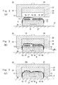
- Reference numeral 1 in Figure 1 represents a first embodiment of a compression bonding device of the present invention.
- This compression bonding device 1 has a platform 9, a drive unit 25, a pressing head 20 and a pedestal 26.
- the pressing head 20 has a head body 21, a dam member 24 and a bonding part 22.
- the head body 21 is in the shape of a plate and is formed of metal such that the head body 21 does not deform when the head body 21 presses the object to be pressed 10, described later.
- the bonding part 22 is formed of an internally homogeneous elastic material (e.g., rubber); and, in contrast to metal materials such as iron, the bonding part 22 deforms when a force is applied thereto, and returns to the original shape when the force is removed.
- the bonding part 22 is fixed on the surface of the head body 21.
- the pressing head 20 is placed above the platform 9 with the bonding part 22 facing downward.
- the pressing head 20 is connected to the drive unit 25, so that when the drive unit 25 is activated, the pressing head 20 moves vertically upward and downward above the platform 9 with the exposed face of the bonding part 22 facing downward.
- the head body 21 has a quadrangular shape in plan view, and the bonding part 22 is in the form of a quadratic prism.
- the size of the head body 21 is larger than that of the bonding part 22.
- a cylindrical dam member 24 is placed on the head body 21 externally extending over the bonding part 22 so as to surround the bonding part 22.
- the dam member 24 is made from the same metal as that of the head body 21, and the dam member 24 is fixed to the head body 21.
- the edge of the dammember 24 projects from the surface of the bonding part 22, and a concave portion 29 is formed, which has the inside face of the dam member 24 as a side face and the surface of the bonding part 22 as a bottom face.
- the inside face of the dam member 24 is nearly perpendicular to a horizontal plane, and the surface of the bonding part 22 is nearly horizontal.
- the height of the edge of the dam member 24 from the surface of the bonding part 22 is uniform.
- an opening 23 formed by the edges of the dam member 24 lies in a horizontal plane and has the same quadrangular shape as that of the bottom face of the concave portion 29.
- the pedestal 26 is in the form of a quadratic prism and is placed upright on the platform 9 with one base end surface being in close contact with the surface of the platform 9.
- the other base end surface of the pedestal 26 is a mounting face 27 on which the object to be pressed, described later, is to be mounted.
- the mounting face 27 is parallel with the surface of the platform 9, so that the mounting face 27 is nearly horizontal.
- the mounting face 27 has the same shape as that of the opening 23 of the concave portion 29 or a similar shape slightly smaller than the opening 23 of the concave portion 29 ( Figure 2 ) so that the part of the pedestal 26 on which the mounting face 27 lies can be inserted into the concave portion 29.
- Reference numeral 10 in Figure 3 (a) represents an object to be pressed.
- the object to be pressed 10 has a substrate 11, an anisotropic conductive film 15, and electric components 16, 18.
- the anisotropic conductive film 15 is placed on terminals 12 of the substrate 11.
- the electric components 16, 18 are placed on the side of the anisotropic conductive film 15 opposite to the substrate 11.
- the electric components 16, 18 have terminals 17, 19 such as bumps or lands.
- the terminals 17, 19 of the electric components 16, 18 are placed above the terminals 12 of the substrate 11.
- the electric components 16, 18 are individually mounted on the anisotropic conductive film 15 by a mounting head, not shown, and then pressed by a small pressure with the mounting head while they are preliminarily heated at a relatively low temperature.
- Electric components 16, 18 are tentatively bonded to the substrate 11 by an adhesive force developed by the anisotropic conductive film 15 (tentative compression bonding) .
- the adhesive force during tentative bonding is so weak that the electric components 16, 18 readily fall off the substrate 11.
- the terminals 12 of the substrate 11 and the terminals 17, 19 of the electric components 16, 18 are in neither physical nor mechanical contact with each other, and the anisotropic conductive film 15 exists between them.
- the surface of the substrate 11 on which the electric components 16, 18 are not placed is flat so that the object to be pressed 10 can be mounted on the pedestal 26 with the flat surface being in close contact with the mounting face 27.
- the anisotropic conductive film 15 is larger than the electric components 16, 18 and partially extends over the electric components 16, 18 so that the anisotropic conductive film 15 is exposed between the electric components 16 and 18. Even if the anisotropic conductive film 15 is not exposed between the electric components 16, 18, the anisotropic conductive film 15 partially extends over the outer peripheries of the electric components 16, 18 when it is pressed during the pressing step, described later.
- the bonding part 22 has a surface formed of a material that can be bonded to the anisotropic conductive film 15, and therefore, a protective film 5 having low adhesiveness to the anisotropic conductive film 15 is placed on the surface of the object to be pressed 10 so as to prevent the bonding part 22 and the anisotropic conductive film 15 from contacting each other during the pressing step, described later ( Figure 3(a) ).
- the mounting face 27 is smaller than the opening 23 and the protective film 5 is larger than the mounting face 27 so that the outer periphery of the pedestal 26 including the protective film 5 hanging along the side face of the pedestal 26 at the edge approximately equals to the size of the opening 23.
- the pressing head 20 and the pedestal 26 are aligned so that the opening 23 conforms to the outer periphery of the pedestal 26 including the protective film 5, and when the pressing head 20 is lowered by the drive unit 25, the pedestal 26 is inserted into the concave portion 29 together with the protective film 5.
- the protective film 5 is formed of a compressively deformable material.
- the pedestal 26 can be inserted into the concave portion 29 even if the outer shape of the pedestal 26, including the protective film 5, is slightly larger than the opening 23.
- the electric components 16, 18 can be, for example, semiconductor elements or resistance components, and can have different thicknesses depending on the type of the component.
- the thickness difference between the electric components 16 and 18 forms a step on the surface of the substrate 11.
- Figure 3(b) shows a state in which the bonding part 22 is in contact with the thickest electric component 16 on the substrate 11 via the protective film 5 before the mounting face 27 of the pedestal 26 is inserted into the concave portion 29 together with the object to be pressed 10.
- the bonding part 22 presses the electric components 16, 18 of the object to be pressed 10.
- the mounting face 27 lies above the opening 23 and the edge portion of the side face of the pedestal 26 on the side of the mounting face 27 is inserted into the concave portion 29 and surrounded by the inside face of the dam member 24.
- the side face of the bonding part 22 is not fixed to the dam member 24, and the bonding part 22 is depressed in not only central but also peripheral regions.
- the pressing head 20 is further lowered, and presses the electric components, the electric components are successively contacted with and pressed by the surface of the bonding part 22 in the order of thickness from the thicker electric component 16 to thinner electric component 18.
- the bonding part 22 When the bonding part 22 is depressed upon contact with the electric components 16, 18, the other regions of the bonding part not contacting the electric components 16, 18 bulge by the rebound. However, the bonding part 22 does not bulge horizontally outward. Instead, the surface of the bonding part 22 that does not face the electric components 16, 18 bulges downward as compared with before because the bonding part 22 is fixed to the head body 21 at the bottom face and surrounded by the dam member 24 at the side face. Thus, the surface of the bonding part 22 bulges downward at regions between the electric components 16, 18 and around the object to be pressed 10 ( Figure 3(c) ).
- the anisotropic conductive film 15 may be exposed between the electric components 16 and 18 or the anisotropic conductive film 15 may partially extend over the outer peripheries of the electric components 16, 18 when the electric components 16, 18 are pressed.
- the bonding part 22 does not directly come into contact with the anisotropic conductive film 15 because the spaces between the electric components 16, 18 and the electric components 16, 18 themselves are covered with the protective film 5.
- the clearance between the pedestal 26 and the dam member 24 is so small that the bonding part 22 does not flow out from the clearance even if the surface of it bulges downward around the object to be pressed 10. That is, the downward bulging regions of the bonding part 22 may be filled in the cavities between the electric components 16 and 18, but the bonding part 22 does not radially flow outward in contrast to conventional methods. Thus, no outward force is exerted on the electric components 16, 18 and the electric components 16, 18 are not misaligned.
- the pedestal 26 has a heater 8.
- the object to be pressed 10 is heated at a predetermined temperature by applying a current to the heater 8.
- the flowability of the anisotropic conductive film 15 is increased by heating.
- the anisotropic conductive film 15 is thrust aside by the electric components 16, 18, and the terminals 17, 19 of the electric components 16, 18 are pressed against the terminals 12 of the substrate 11 with electrically conductive particles in the anisotropic conductive film 15, therebetween.
- the electric components 16, 18 and the substrate 11 are electrically connected to each other.
- the anisotropic conductive film 15 contains a thermosetting resin, the anisotropic conductive film 15 can be cured by heating. If the anisotropic conductive film 15 contains a thermoplastic resin, the anisotropic conductive film 15 can become solidified when the temperature drops after completion of heating. Thus, the electric components 16, 18 also are mechanically connected to the substrate 11 via the cured or solidified anisotropic conductive film 15, thereby producing an electric device 10a in which the electric components 16, 18 have been mechanically and electrically connected to the substrate 11.
- the electric device 10a has higher reliable connection because none of the electric components 16, 18 are misaligned when the electric components 16, 18 are pressed.
- the bonding part 22 is not bonded to the anisotropic conductive film 15 because the bonding part 22 does not come into contact with the anisotropic conductive film 15 when it presses the electric components 16, 18. Therefore, once the pressing head 20 is raised, the surface of the bonding part 22 is easily separated from the electric device 10a, and the electric device 10a is left on the pedestal 26.
- the bonding part 22 When the bonding part 22 is separated from the electric device 10a, the force applied to the bonding part 22 is removed and the bonding part 22 returns to the original shape that it had before the bonding part 22 pressed the electric components 16, 18.
- electric components 16, 18 can be continuously connected by the process shown in Figures 3(a)-(c) and described above.
- the height of the edge of the dammember 24 is not specifically limited, but the amount by which the bonding part 22 bulges downward when it presses the object to be pressed 10 does not exceed the maximum thickness of the object to be pressed 10. Therefore, the bonding part 22 does not bulge out from under the dam member 24 if the height from the surface of the bonding part 22 to the edge of the dam member 24 before the bonding part 22 is pressed is equal to or greater than the total of the thickness of the thickest electric component 16 (e. g., semiconductor element) plus the thickness of the substrate 11.
- the thickest electric component 16 e. g., semiconductor element
- Reference numeral 3 in Figure 4(a) represents a compression bonding device according to a second embodiment.
- the compression bonding device 3 has the same structure as that of the compression bonding device 1 according to the first embodiment.
- the layout of the pressing head 30 and the pedestal 26 also is the same as that of the compression bonding device 1 according to the first embodiment except that the bonding part 34 of the pressing head 30 is changed as follows.
- the bonding part 34 of the compression bonding device 3 has a movable plate 33, a compression member 31, and a pressing rubber 32 formed of the same rubber as that of the bonding part 22 of the compression bonding device 1 according to the first embodiment.
- the compression member 31 is formed of a material having internal cavities that are collapsed under pressure to decrease the volume, such as sponge-like rubber.
- the upper end of the compression member 31 is fixed to the surface of the head body 21, the surface of the movable plate 33 is fitted to the lower end of the compression member 31, and the upper end of the pressing rubber 32 is fitted to the back face of the movable plate 33.
- the compression member 31, movable plate 33 and pressing rubber 32 are arranged in the order as described from the head body 21 toward a downward vertical direction where the pedestal 26 lies.
- the compression member 31 has the same columnar shape in horizontal section as the sectional shape of a region surrounded by the dam member 24. Thus, the side face of the compression member 31 is in contact with the inside face of the dam member 24, but is not fixed to the dam member 24.
- the pressing rubber 32 and movable plate 33 also are unfixed to the dam member 24, and are movable within the region surrounded by the dam member 24.
- Figure 4(b) shows a state in which the pressing head 30 is further lowered after the pressing rubber 32 has been contacted with the protective film 5 on the object to be pressed 10.
- the force required to deform the compression member 31 is smaller than the force required to deform the pressing rubber 32.
- the compression member 31 is pressed against the head body 21 by the pressing rubber 32 and the compression member 31 is compressed and reduced in thickness before the pressing rubber 32 deforms.
- the compression member 31 is pressed by the pressing rubber 32, whereby a concave portion, which does not exist before the compression member 31 is compressed by the pressing head 30, is formed.
- the compression of the compression member 31 stops when the compression member 31 deforms to some extent due to the limitation of the amount by which the compression member 31 can deform. If the pressing head 30 is lowered further, the pressing rubber 32 deforms ( Figure 4(c) ).
- the configuration of the compression member 31 is not specifically limited so long as the configuration of the compression member 31 allows the compression member 31 to decrease in volume by pressing.
- the pressing head represented by reference numeral 35 in Figure 5 has the same structure as that of the pressing head 3 shown in Figures 4 (a) - (c) except that the compressionmember differs, as described below. The same members in the pressing head 35 are explained with the same reference numbers of the pressing head 3.
- the compression member of this pressing head 35 is comprised of a spring 36.
- the spring 36 may be compressed by pressing to raise the surface of the bonding part 34, whereby the edge of the dam member 24 may project below the bonding part 34.
- Reference numeral 4 in Figure 6 represents a compression bonding device according to a third embodiment.
- Compression bonding device 4 has the same structure as that of the compression bonding device 1 according to the first embodiment, except that a dam member is not provided on the pressing head 40.
- the dam member 49 is provided around the mounting face of the pedestal 46, as discussed below.
- the bonding part 42 has a pressing rubber that is fitted to the surface of the head body 41 in the same manner as in the compression bonding device 1 according to the first embodiment.
- the bonding part 42 is surrounded by a sliding plate 44 formed of a thin plate instead of a dam member.
- the pedestal 46 is columnar in the same manner as in the compression bonding device 1 according to the first embodiment.
- the dam member 49 is fixed to the pedestal 46 around the mounting face 47 so as to surround the mounting face 47.
- the edge of the dam member 49 projects above the mounting face 47 to form a concave portion 45 having the inside face of the dam member 49 as a side face, and the mounting face 47 as a bottom face.
- Figure 7 is a schematic plan view for comparing the planar shape of the pedestal 46 and the planar shape of the pressing head 40.
- the outer periphery including the sliding plate 44 of the bonding part 42 is equal to or smaller than the opening 48 of the concave portion 45.
- the side face of the bonding part 42 is directed vertically downward and the side face of the sliding plate 44 is also directed vertically downward because the thickness of the sliding plate 44 is uniform.
- the inside face of the dam member 49 is directed vertically downward, whereby the lower end of the pressing head 40 can be inserted into the concave portion 45.
- the opening 48 of the concave portion 45 is larger than the outer periphery of the planar shape of the pressing head 40.
- the protective film 5 is large enough to cover the side face and the periphery of the concave portion 45 by its edge so that the size of the opening 48 of the concave portion 45 narrowed by covering the opening 48 with the protective film 5 approximately equals the size of the outer periphery of the planar shape of the pressing head 40.
- FIG 8 (b) shows a state in which the lower end of the pressing head 40 is inserted into the opening 48 and the surface of the bonding part 42 is in contact with the thickest electric component 16 via the protective film 5. In this state, the bonding part 42 is not pressed and not deformed.
- the side face of the bonding part 42 is surrounded by the dam member 49 from the surface of the bonding part 42 to the bottom face if the sliding plate 44 is flexible, or at least the periphery of the surface of the bonding part 42 is surrounded by the dam member 49 if the sliding plate 44 is not flexible.
- the side face of the bonding part 42 is surrounded by a rigid member in either case.
- the bonding part 42 does not bulge horizontally outward. Instead, its surface bulges downward ( Figure 8(c) ).
- the distance from the edge of the surface of the bonding part 42 to the dam member 49 is short because the sliding plate 44 is thin and the clearance between the pressing head 40 and the dam member 49 is also small. Even if the bonding part 42 is raised and extends outward, the bonding part 42 is stopped by the dam member 49 and therefore, the amount of extension is small and the electric components 16, 18 are less likely to be misaligned.
- the clearance between the dam member 49 and the side face of the pressing head 40 may be filled with the protective film 5 by designing the protective film 5 as thick as possible.
- the dam member is fixed to the head body 21 or pedestal 46, but the present invention is not limited to such cases, and the dam member may be formed of a member that is separate from the pedestal or the head body, and the dam member may be in close contact with the pedestal or the head body when the object to be pressed 10 is pressed.
- Reference numeral 7 in Figure 10(a) represents a compression bonding device according to a fourth embodiment.
- the compression bonding device 7 has the same structure as that of the compression bonding device 1 according to the first embodiment, and the layout of the pressing head 70 and the pedestal 26 is also similar except that the dam member 74 of the pressing head 70 is formed of a member that is separate from the head body 71.
- Figure 10(a) shows that a state in which the dam member 74 is separated from the head body 71.
- the dam member 74 has a plurality of plate-shaped unit members 75, as shown in Figure 11 .
- the unit members 75 arranged along the side face of the bonding part 72 have their surfaces vertically oriented and to be in close contact with the head body 71 by moving means, not shown. In the state where each unit member 75 is in close contact with the head body 71, the side face of the bonding part 72 is surrounded by the unit members 75.
- Figure 10(b) shows a state in which the bonding part 72 is in contact with the protective film 5 on the thickest electric component 16, and the bonding part 72 is not pressed and not deformed.
- the unit members 75 should be brought into close contact with the head body at the latest in this state.
- the side face of the bonding part 72 may be surrounded by the unit members 75 when the bonding part 72 is pressed and deformed.
- each unit member 75 should be fitted to project at the lower end from the surface of the bonding part 72 before the bonding part 72 is pressed so that the bonding part 72 may not bulge out from under the dam member 74 even if the pressing head 70 is further lowered to press the bonding part 72 in the same manner as with the compression bonding device 1 according to the first embodiment, so that the electric components 16, 18 are not misaligned ( Figure 10(c) ).
- the bonding part 72 may be also formed of a pressing rubber and a compression member.
- Reference numerals 90 and 95 in Figures 16 and 17 represent pressing heads in which a dam member 74 can be separated from a head body 71 and a bonding part 72 has compression members 31, 36 and a pressing rubber 32.
- the pressing head 90 in Figure 16 has the same structure as that of the bonding part 34 of the pressing head 17 in Figures 4(a)-(c)
- the pressing head 95 in Figure 17 has the same structure as that of the bonding part 34 of the pressing head 35 in Figure 5 .
- the layout of the head body 71 and the dam member 75 is similar to that of the pressing head 70 in Figure 10 and will be explained with the same reference numerals for the same members.
- the pressing heads 90, 95 can also be designed in such a manner that, when the dam member 74 is fitted to the head body 71, the edge of the dam member 74 may be flush with the surface of the bonding part 34 before the bonding part 34 is pressed.
- the surface of the bonding part 34, before the bonding part 34 is pressed may project below the edge of the dam member 74, or the edge of the dam member 74 may project below the surface of the bonding part 34 before the bonding part 34 is pressed so long as a concave potion having the surface of the pressing rubber 32 as a bottom face is subsequently formed by compression of the compression member 31.
- the dam member 78 may be initially cylindrically shaped as shown in Figure 12 .
- the pressing head 70 is inserted into the cylinder of the dam member 78 and the bonding part 72 is surrounded by the inner periphery surface of the dam member 78 before the object to be pressed 10 is pressed and the bonding part 72 is deformed.
- misalignment of the electric components 16, 18 can be prevented because lateral extension of the bonding part 72 is stopped by the dam member 78.
- Reference numeral 8 in Figure 13 (a) represents a compression bonding device according to a fifth embodiment of the present invention.
- the compression bonding device 8 has the same structure as that of the compression bonding device 4 according to the third embodiment described above.
- the layout of the pedestal 86 and the pressing head 40 is also similar except that the dam member 89 is another member that can be separated from the pedestal 86.
- Figure 13(a) shows a state in which the dam member 89 is separated from the pedestal 86.
- the dam member 89 may be formed of a plurality of unit members as shown in Figure 11 or may be formed of a single cylinder as shown in Figure 12 .
- each unit member is arranged along the edge of the mounting face 87 and is in close contact with the mounting face 87 so as to surround the mounting face 87.
- the dam member 89 is cylindrical, the pedestal 86 is inserted into the lower end of the cylinder, thereby bringing the dam member 89 into close contact with the pedestal 86.
- the edge of the dam member 89 projects above the mounting face 87, whereby a concave portion 85 is formed, which has the inner peripheral surface of the dam member 89 as a side face and the mounting face 87 as a bottom face.
- FIG. 13(b) shows a state in which the bonding part 42 is in contact with the thickest electric component 16 of the object to be pressed 10 on the mounting face 87 via the protective film 5. In this state, the bonding part 42 is not pressed and not deformed. At latest in this state, the dam member 89 should be brought into close contact with the pedestal 86, to thereby surround the mounting face 87 by the dam member 89.
- the protective film 5 is not entangled between the dam member 89 and the pedestal 86 by fitting the dam member 89 to the pedestal 86 and then applying the protective film 5 thereon.
- the protective film 5 may be wound around the pressing head 40 rather than being applied on the mounting face 87. Further, the pressing head 40 may be pressed against the object to be pressed 10 while the surface of the bonding part 42 is covered.
- the present invention is not limited to such cases.
- one or more slits 99 may be formed in the dam member 24, and the side face of the bonding part 22 may be partially exposed, as shown in Figure 15 , so that horizontal extension of the bonding part 22 can be prevented when the object to be pressed 10 is pressed.
- the shape and size of the protective film 5 are not specifically limited.
- a protective film 5 having a size that does not extend over the mounting faces 27, 47, 87 may be used, or a protective film 5 covering only a partial surface of the object to be pressed 10 may be used, as long as any contact can be avoided between the anisotropic conductive film 15 and the bonding parts 22, 34, 42, 72.
- the bonding parts 22, 34, 42, 72 may be brought into direct contact with the object to be pressed 10 without using the protective film 5.
- the material from which the pressing rubber is formed may be changed to one having low adhesiveness to the anisotropic conductive film 15, or a release layer having releasability against the anisotropic conductive film 15 may be provided on the surface of the pressing rubber.
- the compression bonding devices of the present application can connect electric components to a substrate without using a protective film 5.
- the clearance can be decreased by covering the side face of the dam member with a protective film 5.
- the pedestal, dam member and pressing head can be manufactured at low costs without using a mold or the like, and even if the molding precision is low, the clearance between the dam member and the pressing head or between the dam member and the pedestal can be filled by appropriately selecting the thickness of the protective film 5.
- the type of the substrate 11 used in the present invention is not specifically limited, and various substrates such as rigid substrates and flexible substrate can be used.
- the type of the electric component to be connected to the substrate 11 is not specifically limited. Furthermore, the compression bonding devices and connecting processes of the present application can be used to connect not only electric components but also another substrate onto the substrate 11.
- the anisotropic conductive film 15 may contain either one or both of a thermoplastic resin and a thermosetting resin.
- thermosetting resin and thermoplastic resin are not specifically limited.
- one ormore thermosetting resins such as epoxy resins, acrylic resins and urethane resins can be used, and one or more thermoplastic resins such as phenoxy resins and polyvinyl alcohols can be used.
- the type of conductive particles is not specifically limited. For instance, not only metal particles but also resin particles coated with a metal layer can be used.
- a pasty anisotropic conductive adhesive may be applied on the surface of the substrate 11 and electric components may be bonded to the anisotropic conductive adhesive, thereby obtaining an object to be pressed 10.
- the type of the protective film is not specifically limited, but preferably has releasability against the anisotropic conductive film 15 described above, e.g., a molded film of polytetrafluoroethylene or a molded film of silicone rubber.
- the elastic material forming the pressing rubber is not specifically limited, and elastomers having rubber hardnesses (according to JIS S 6050) of 40, 80 could be used by way of example.
- Rubber hardness is determined by the method described in "6. Test method” in JIS S 6050:2002, as follows.
- Samples having stood for 24 hours or more after production are used for the test.
- General matters common to chemical analyses are as shown in JIS K 0050.
- a hardness tester is used in a test for hardness. The surface of a test sample piece horizontally held is brought into contact with the pressurizing face while the intender point of the tester is vertical. Then, the scale is immediately read as a positive number. As to the measurement point of the test sample piece, the entire surface of the test sample piece is divided into three, each center portion is measured individually, and then their median values become hardness of the test sample piece.
- the hardness tester here refers to a spring hardness tester having a semi-circular indenter point of 5.08 mm ⁇ 0.02 mm in diameter.
- the height of the indenter point is 2.54 ⁇ 0.22 mm at scale 0, and 0 mm at scale 100.
- Table 1 Tab. 1 Relationship between scale and spring force Scale 0 10 20 25 30 40 50 60 70 75 80 90 100 Spring Force N 0.54 1.32 2.11 2.50 2.89 3.68 4.46 5.25 6.03 6.42 6.82 7.60 8.39
- Elastomers used for the pressing rubber may include both natural and synthetic rubbers, and preferably silicone rubber in terms of heat resistance and pressure resistance.
- the present invention is not limited to such cases.
- the platform 9 may be vertically moved upward and downward while the pressing head 20 is fixed, or both of the pressing head 20 and the platform 9 may be vertically moved upward and downward so far as the pressing head 20 and the platform 9 are relatively moved.
- a semiconductor element 16 and a substrate 11 were connected by using the compression bonding device 1 according to the first embodiment with varying heights from the surface of the bonding part 22 to the edge of the dam member 24 before the bonding part 22 is pressed (edge height). The amount of horizontal displacement of the semiconductor element 16 was measured.
- the distance (clearance) from the side face of the pressing head 20 to the inner wall face of the dam member 24 was 50 ⁇ m when the pressing head 20 was inserted into the concave portion 29.
- a protective film 5 having a thickness of 50 ⁇ m a pressure was applied with substantially no clearance between the pressing head 20 and the dam member 24.
- the thickness of the semiconductor element 16 was 0.4 mm, and the thickness of the substrate 11 was 0.6 mm.
- the maximum amount of displacement of the semiconductor element 16 measured is shown in Table 2 below along with the edge height of the dam member 24.
- Table 2 Tab. 2 Edge height of a dam member and maximum amount of displacement Edge heigh (mm) Maximum amount of displacement (mm) -3.0 0.050 -1.0 0.050 0 0.050 1.0 0. 020 2.0 0.015 3.0 0. 015
- the maximum amount of displacement becomes small when the edge of the dam member 24 projects from the surface of the bonding part 22 before the bonding part 22 is pressed, while the amount of displacement of the semiconductor element 16 is large when the surface of the bonding part 22 is flush with the edge of the dam member 24 or projects from the edge of the dam member 24.
Landscapes
- Engineering & Computer Science (AREA)
- Microelectronics & Electronic Packaging (AREA)
- Computer Hardware Design (AREA)
- Power Engineering (AREA)
- Manufacturing & Machinery (AREA)
- Mechanical Engineering (AREA)
- Physics & Mathematics (AREA)
- Condensed Matter Physics & Semiconductors (AREA)
- General Physics & Mathematics (AREA)
- Fluid Mechanics (AREA)
- Wire Bonding (AREA)
- Electric Connection Of Electric Components To Printed Circuits (AREA)
Abstract


Description
- The present invention generally relates to a compression bonding device for packaging electric components on a substrate and packaging processes therefor.
- Conventionally, packaging processes for connecting electric components such as semiconductor elements to a substrate have used a compression bonding device by which the electric components are pressed against the substrate with a pressing head under heat.
-
Reference numeral 101 inFigure 18(a) represents a conventional compression bonding device. Thecompression bonding device 101 has apedestal 126 and apressing head 120. - The
pressing head 120 has a pressing rubber fitted into a metal frame, or a pressing rubber bonded to a metal plate with an adhesive or a liquid rubber cast into a metal frame and cured within the metal frame, etc. - In the case of a
pressing rubber 122 fitted into ahead body 121 made from a metal frame, the surface of thepressing rubber 122 is flush with the surface of thehead body 121 or projects below the surface of thehead body 121. When thepressing head 120 is pressed against an object to be pressed 110 on thepedestal 126, the surface of thepressing rubber 122 comes into contact with the object to be pressed 110. - The object to be pressed 110 has a
substrate 111 andelectric components substrate 111 so that steps are formed on thesubstrate 111 due to the thickness differences between theelectric components - The
pressing rubber 122 is formed of an elastic material that deforms under pressure. Thepressing rubber 122 first comes into contact with the thickestelectric component 116. Then, thepressing rubber 122 deforms and successively comes into contact with the electric components in the order of thickness from the thickestelectric component 116 to thinnestelectric component 118. Finally, all of theelectric components pressing rubber 122. - Before the
electric components compression bonding device 101, theelectric components substrate 111 are aligned; and terminals of theelectric components substrate 111 with an adhesive 115 inserted therebetween. - The surface of the
pedestal 126 is nearly horizontal, and thesubstrate 111 is horizontally placed on that surface. When thepressing head 120 is vertically moved downward to press theelectric components electric components substrate 111 come into contact with each other, thereby electrically connecting theelectric components Figure 18(b) ), because theelectric components adhesive 115 aside and move toward the terminals of thesubstrate 111. Thus, the conventionalcompression bonding device 101 can simultaneously connect electric components having different thicknesses to one substrate. - However, if the
pressing rubber 122 is depressed when it pressescomponents pressing rubber 122 has the property of bulging around the depressed part. Therefore, the bulging part of thepressing rubber 122 climbs over the frame of thehead body 121 with the result that the surface of thepressing rubber 122 extends horizontally outward. -
Figure 19 is a plan view showing the manner in which the surface of thepressing rubber 122 extends horizontally outward, i.e., thepressing rubber 122 radially flows around the center C of its planar shape. Due to the greater amount of movement at the periphery of thepressing rubber 122 as compared with the vicinity of the center C, theelectric components pressing rubber 122 horizontally move as thepressing rubber 122 extends, whereby the terminals of theelectric components substrate 111. - If the
electric components electric components substrate 111, resulting in the deterioration of a reliable connection between theelectric components substrate 111. - Patent document 1:
JP A 2002-359264 - Patent document 2:
JP A 2005-32952 - The present invention is made to address the problems described above, and its purpose is to provide a compression bonding device capable of reliably connecting electric components to a substrate.
- In order to address the problems described above, according to one aspect of the present invention there is provided a compression bonding device comprising a pedestal, a dam member and a pressing head. The pressing head and the pedestal are movable relative to one another to press an object to be pressed placed on a mounting face of the pedestal with the pressing head. The pressing head comprises a head body and a pressing rubber which is placed in the head body, and the dam member extends beyond the surface level of the pressing rubber and is placed around the pressing rubber, and wherein the pressing rubber, by deforming, presses the object to be pressed placed on the mounting face of the pedestal when the pressing head and the pedestal are moved relative to one another.
- According to some aspects, the present invention provides the compression bonding device wherein the pedestal is inserted into a space surrounded by the dam member.
- According to one aspect, the present invention provides the compression bonding device wherein the dam member is separable from the head body.
- According to yet another aspect of the present invention, there is provided a compression bonding device comprising a pedestal and a pressing head. The pressing head and the pedestal are movable relative to one another to press an object to be pressed placed on a mounting face of the pedestal with the pressing head. The pressing head comprises a head body and a pressing rubber which is placed in the head body, and the mounting face is surrounded by a dam member having a surface level that extends beyond the mounting face.
- According to another aspect, the present invention provides the compression bonding device wherein the pressing head is inserted into a space surrounded by the dam member.
- According to yet another aspect, the present invention provides the compression bonding device wherein the dam member is separable from the pedestal.
- According to a further aspect, the present invention provides the compression bonding device wherein a compressively deformable compression member is placed between the pressing rubber and the head body, and at least when the compression member is compressed, the dam member becomes higher than the surface level of the pressing rubber.
- According to another aspect of the present invention, there is provided a component packaging process comprising placing, on a mounting face of a pedestal, an object to be pressed including a substrate and a plurality of components having different heights on the substrate and pressing the components with a pressing rubber provided on a pressing head and fixing the components to the substrate. The object is surrounded by a dam member and the lateral flow of the pressing rubber due to deformation of the pressing rubber is stopped by the dam member when the pressing rubber presses the components.
- In another aspect, the present invention provides the packaging process comprising placing an anisotropic conductive film between the components and the substrate to bond the components to the substrate, and then pressing the components with the pressing rubber while heating the substrate.
- In another aspect, the present invention provides the packaging process comprising placing a protective film that is releasable from the anisotropic conductive film between the pressing rubber and the object to be pressed when the components are pressed.
- When the pressing rubber is pressed against the object to be pressed, the electric components are less likely to be misaligned even at the periphery of the pressing rubber because the pressing rubber is prevented from lateral extension by the dam member. As a result of the absence of lateral extension of the pressing rubber, nearly the total force for deforming the pressing rubber converts into a force for pressing the object to be pressed, thereby avoiding wasted pressure during pressing.
-
-
Figure 1 is a sectional diagram for illustrating a compression bonding device according to a first embodiment; -
Figure 2 is a plan view for illustrating the geometry of the pressing head and the pedestal; -
Figures 3(a)-(c) are sectional diagrams for illustrating a process for packaging electric components on a substrate; -
Figures 4(a)-(c) are sectional diagrams for illustrating a process for packaging electric components using a compression bonding device according to a second embodiment; -
Figure 5 is a sectional diagram for illustrating another embodiment of the pressing head; -
Figure 6 is a sectional diagram for illustrating a compression bonding device according to a third embodiment; -
Figure 7 is a plan view for illustrating the geometry of the pressing head and the pedestal; -
Figures 8(a)-(c) are sectional diagrams for illustrating a process for packaging electric components on a substrate; -
Figure 9 is a sectional diagram for illustrating another embodiment of the pressing head; -
Figures 10(a)-(c) are sectional diagrams for illustrating a process for packaging electric components on a substrate using a compression bonding device according to a fourth embodiment; -
Figure 11 is a plan view for illustrating an embodiment of a dam member; -
Figure 12 is a plan view for illustrating another embodiment of a dam member; -
Figures 13(a)-(c) are sectional diagrams for illustrating a process for packaging electric components on a substrate using a compression bonding device according to a fifth embodiment; -
Figure 14 is a sectional diagram for illustrating another embodiment of a method for placing a protective film; -
Figure 15 is a side view for illustrating another embodiment of a dam member; -
Figure 16 is a sectional diagram for illustrating another embodiment of a pressing head having a separable dam member; -
Figure 17 is a sectional diagram for illustrating another embodiment of a pressing head having a separable dam member; -
Figures 18 (a) and (b) are sectional diagrams for illustrating a conventional packaging process; -
Figure 19 is a plan view for illustrating extension of a pressing rubber. -
- 1, 3, 4: compression bonding device;
- 5: protective film;
- 10: object to be pressed;
- 11: substrate;
- 15: anisotropic conductive film;
- 16, 18: electric components;
- 20, 30, 35, 40, 70: pressing head;
- 21: head body;
- 22: bonding part (pressing rubber);
- 31: compression member;
- 32: pressing rubber;
- 24, 49, 74, 78, 89: dam member;
- 26, 46, 86: pedestal.
-
Reference numeral 1 inFigure 1 represents a first embodiment of a compression bonding device of the present invention. Thiscompression bonding device 1 has aplatform 9, adrive unit 25, apressing head 20 and apedestal 26. Thepressing head 20 has ahead body 21, adam member 24 and abonding part 22. - In this embodiment, the
head body 21 is in the shape of a plate and is formed of metal such that thehead body 21 does not deform when thehead body 21 presses the object to be pressed 10, described later. Thebonding part 22 is formed of an internally homogeneous elastic material (e.g., rubber); and, in contrast to metal materials such as iron, thebonding part 22 deforms when a force is applied thereto, and returns to the original shape when the force is removed. - The
bonding part 22 is fixed on the surface of thehead body 21. Thepressing head 20 is placed above theplatform 9 with thebonding part 22 facing downward. - The
pressing head 20 is connected to thedrive unit 25, so that when thedrive unit 25 is activated, thepressing head 20 moves vertically upward and downward above theplatform 9 with the exposed face of thebonding part 22 facing downward. - The
head body 21 has a quadrangular shape in plan view, and thebonding part 22 is in the form of a quadratic prism. The size of thehead body 21 is larger than that of thebonding part 22. Acylindrical dam member 24 is placed on thehead body 21 externally extending over thebonding part 22 so as to surround thebonding part 22. - The
dam member 24 is made from the same metal as that of thehead body 21, and thedam member 24 is fixed to thehead body 21. The edge of thedammember 24 projects from the surface of thebonding part 22, and aconcave portion 29 is formed, which has the inside face of thedam member 24 as a side face and the surface of thebonding part 22 as a bottom face. - The inside face of the
dam member 24 is nearly perpendicular to a horizontal plane, and the surface of thebonding part 22 is nearly horizontal. The height of the edge of thedam member 24 from the surface of thebonding part 22 is uniform. Thus, anopening 23 formed by the edges of thedam member 24 lies in a horizontal plane and has the same quadrangular shape as that of the bottom face of theconcave portion 29. Thepedestal 26 is in the form of a quadratic prism and is placed upright on theplatform 9 with one base end surface being in close contact with the surface of theplatform 9. - The other base end surface of the
pedestal 26 is a mountingface 27 on which the object to be pressed, described later, is to be mounted. The mountingface 27 is parallel with the surface of theplatform 9, so that the mountingface 27 is nearly horizontal. The mountingface 27 has the same shape as that of theopening 23 of theconcave portion 29 or a similar shape slightly smaller than theopening 23 of the concave portion 29 (Figure 2 ) so that the part of thepedestal 26 on which the mountingface 27 lies can be inserted into theconcave portion 29. - Next, a process for connecting electric components such as a semiconductor element to a substrate using this
compression bonding device 1 is explained.Reference numeral 10 inFigure 3 (a) represents an object to be pressed. The object to be pressed 10 has asubstrate 11, an anisotropicconductive film 15, andelectric components - The anisotropic
conductive film 15 is placed onterminals 12 of thesubstrate 11. Theelectric components conductive film 15 opposite to thesubstrate 11. Theelectric components terminals terminals electric components terminals 12 of thesubstrate 11. - The
electric components conductive film 15 by a mounting head, not shown, and then pressed by a small pressure with the mounting head while they are preliminarily heated at a relatively low temperature.Electric components substrate 11 by an adhesive force developed by the anisotropic conductive film 15 (tentative compression bonding) . However, the adhesive force during tentative bonding is so weak that theelectric components substrate 11. Theterminals 12 of thesubstrate 11 and theterminals electric components conductive film 15 exists between them. - The surface of the
substrate 11 on which theelectric components pedestal 26 with the flat surface being in close contact with the mountingface 27. - The anisotropic
conductive film 15 is larger than theelectric components electric components conductive film 15 is exposed between theelectric components conductive film 15 is not exposed between theelectric components conductive film 15 partially extends over the outer peripheries of theelectric components - The
bonding part 22 has a surface formed of a material that can be bonded to the anisotropicconductive film 15, and therefore, aprotective film 5 having low adhesiveness to the anisotropicconductive film 15 is placed on the surface of the object to be pressed 10 so as to prevent thebonding part 22 and the anisotropicconductive film 15 from contacting each other during the pressing step, described later (Figure 3(a) ). - Here, the mounting
face 27 is smaller than theopening 23 and theprotective film 5 is larger than the mountingface 27 so that the outer periphery of thepedestal 26 including theprotective film 5 hanging along the side face of thepedestal 26 at the edge approximately equals to the size of theopening 23. - Thus, when the
pressing head 20 and thepedestal 26 are aligned so that theopening 23 conforms to the outer periphery of thepedestal 26 including theprotective film 5, and when thepressing head 20 is lowered by thedrive unit 25, thepedestal 26 is inserted into theconcave portion 29 together with theprotective film 5. - The
protective film 5 is formed of a compressively deformable material. Thepedestal 26 can be inserted into theconcave portion 29 even if the outer shape of thepedestal 26, including theprotective film 5, is slightly larger than theopening 23. - The
electric components electric components substrate 11. -
Figure 3(b) shows a state in which thebonding part 22 is in contact with the thickestelectric component 16 on thesubstrate 11 via theprotective film 5 before the mountingface 27 of thepedestal 26 is inserted into theconcave portion 29 together with the object to be pressed 10. Thebonding part 22 presses theelectric components face 27 lies above theopening 23 and the edge portion of the side face of thepedestal 26 on the side of the mountingface 27 is inserted into theconcave portion 29 and surrounded by the inside face of thedam member 24. by - When the
pressing head 20 is further lowered from this state and thebonding part 22 is brought relatively close to thesubstrate 11, the part of thebonding part 22 in contact with theelectric component 16 is pressed and deformed. - The side face of the
bonding part 22 is not fixed to thedam member 24, and thebonding part 22 is depressed in not only central but also peripheral regions. When thepressing head 20 is further lowered, and presses the electric components, the electric components are successively contacted with and pressed by the surface of thebonding part 22 in the order of thickness from the thickerelectric component 16 to thinnerelectric component 18. - When the
bonding part 22 is depressed upon contact with theelectric components electric components bonding part 22 does not bulge horizontally outward. Instead, the surface of thebonding part 22 that does not face theelectric components bonding part 22 is fixed to thehead body 21 at the bottom face and surrounded by thedam member 24 at the side face. Thus, the surface of thebonding part 22 bulges downward at regions between theelectric components Figure 3(c) ). - As noted above, the anisotropic
conductive film 15 may be exposed between theelectric components conductive film 15 may partially extend over the outer peripheries of theelectric components electric components bonding part 22 does not directly come into contact with the anisotropicconductive film 15 because the spaces between theelectric components electric components protective film 5. - The clearance between the
pedestal 26 and thedam member 24 is so small that thebonding part 22 does not flow out from the clearance even if the surface of it bulges downward around the object to be pressed 10. That is, the downward bulging regions of thebonding part 22 may be filled in the cavities between theelectric components bonding part 22 does not radially flow outward in contrast to conventional methods. Thus, no outward force is exerted on theelectric components electric components - The
pedestal 26 has aheater 8. The object to be pressed 10 is heated at a predetermined temperature by applying a current to theheater 8. The flowability of the anisotropicconductive film 15 is increased by heating. - Thus, when the
electric components conductive film 15 is thrust aside by theelectric components terminals electric components terminals 12 of thesubstrate 11 with electrically conductive particles in the anisotropicconductive film 15, therebetween. As a result, theelectric components substrate 11 are electrically connected to each other. - If the anisotropic
conductive film 15 contains a thermosetting resin, the anisotropicconductive film 15 can be cured by heating. If the anisotropicconductive film 15 contains a thermoplastic resin, the anisotropicconductive film 15 can become solidified when the temperature drops after completion of heating. Thus, theelectric components substrate 11 via the cured or solidified anisotropicconductive film 15, thereby producing anelectric device 10a in which theelectric components substrate 11. - The
electric device 10a has higher reliable connection because none of theelectric components electric components - As described above, the
bonding part 22 is not bonded to the anisotropicconductive film 15 because thebonding part 22 does not come into contact with the anisotropicconductive film 15 when it presses theelectric components pressing head 20 is raised, the surface of thebonding part 22 is easily separated from theelectric device 10a, and theelectric device 10a is left on thepedestal 26. - When the
bonding part 22 is separated from theelectric device 10a, the force applied to thebonding part 22 is removed and thebonding part 22 returns to the original shape that it had before thebonding part 22 pressed theelectric components - If the
electric device 10a left on thepedestal 26 is removed and a new object to be pressed 10 is mounted on thepedestal 26,electric components Figures 3(a)-(c) and described above. - The height of the edge of the
dammember 24 is not specifically limited, but the amount by which thebonding part 22 bulges downward when it presses the object to be pressed 10 does not exceed the maximum thickness of the object to be pressed 10. Therefore, thebonding part 22 does not bulge out from under thedam member 24 if the height from the surface of thebonding part 22 to the edge of thedam member 24 before thebonding part 22 is pressed is equal to or greater than the total of the thickness of the thickest electric component 16 (e. g., semiconductor element) plus the thickness of thesubstrate 11. - The foregoing description relates to cases in which the
concave portion 29 has been preliminarily formed in thepressing head 20, the object to be pressed 10 is inserted in theconcave portion 29, and thebonding part 22 is then contacted with the object to be pressed 10. However, the present invention is not limited to such cases. -
Reference numeral 3 inFigure 4(a) represents a compression bonding device according to a second embodiment. Thecompression bonding device 3 has the same structure as that of thecompression bonding device 1 according to the first embodiment. The layout of thepressing head 30 and thepedestal 26 also is the same as that of thecompression bonding device 1 according to the first embodiment except that thebonding part 34 of thepressing head 30 is changed as follows. - In contrast to the
bonding part 22 of thecompression bonding device 1 according to the first embodiment, which is formed of rubber, thebonding part 34 of thecompression bonding device 3 has amovable plate 33, acompression member 31, and apressing rubber 32 formed of the same rubber as that of thebonding part 22 of thecompression bonding device 1 according to the first embodiment. Thecompression member 31 is formed of a material having internal cavities that are collapsed under pressure to decrease the volume, such as sponge-like rubber. - The upper end of the
compression member 31 is fixed to the surface of thehead body 21, the surface of themovable plate 33 is fitted to the lower end of thecompression member 31, and the upper end of thepressing rubber 32 is fitted to the back face of themovable plate 33. Thus, thecompression member 31,movable plate 33 and pressingrubber 32 are arranged in the order as described from thehead body 21 toward a downward vertical direction where thepedestal 26 lies. - The
compression member 31 has the same columnar shape in horizontal section as the sectional shape of a region surrounded by thedam member 24. Thus, the side face of thecompression member 31 is in contact with the inside face of thedam member 24, but is not fixed to thedam member 24. The pressingrubber 32 andmovable plate 33 also are unfixed to thedam member 24, and are movable within the region surrounded by thedam member 24. -
Figure 4(b) shows a state in which thepressing head 30 is further lowered after thepressing rubber 32 has been contacted with theprotective film 5 on the object to be pressed 10. - The force required to deform the
compression member 31 is smaller than the force required to deform thepressing rubber 32. When thepressing head 30 is lowered, thecompression member 31 is pressed against thehead body 21 by the pressingrubber 32 and thecompression member 31 is compressed and reduced in thickness before thepressing rubber 32 deforms. Thecompression member 31 is pressed by the pressingrubber 32, whereby a concave portion, which does not exist before thecompression member 31 is compressed by thepressing head 30, is formed. - The compression of the
compression member 31 stops when thecompression member 31 deforms to some extent due to the limitation of the amount by which thecompression member 31 can deform. If thepressing head 30 is lowered further, the pressingrubber 32 deforms (Figure 4(c) ). - When the
pressing rubber 32 deforms, the concave portion described above is formed, and the edge of thedammember 24 projects below the surface of thepressing rubber 32. A clearance between the edge and thepedestal 26 is small. Thus, the pressingrubber 32 does not flow out from the clearance and theelectric components compression bonding device 1 according to the first embodiment. - The configuration of the
compression member 31 is not specifically limited so long as the configuration of thecompression member 31 allows thecompression member 31 to decrease in volume by pressing. The pressing head represented byreference numeral 35 inFigure 5 has the same structure as that of thepressing head 3 shown inFigures 4 (a) - (c) except that the compressionmember differs, as described below. The same members in thepressing head 35 are explained with the same reference numbers of thepressing head 3. - The compression member of this
pressing head 35 is comprised of aspring 36. Thespring 36 may be compressed by pressing to raise the surface of thebonding part 34, whereby the edge of thedam member 24 may project below thebonding part 34. - If the force applied to the
pressing rubber 32 can be transferred to thecompression member 31, there is no special need for providing the supportingplate 33. - The foregoing description relates to cases in which a dam member is provided on the
pressing head 20, but the present invention is not limited to such cases. -
Reference numeral 4 inFigure 6 represents a compression bonding device according to a third embodiment.Compression bonding device 4 has the same structure as that of thecompression bonding device 1 according to the first embodiment, except that a dam member is not provided on thepressing head 40. Thedam member 49 is provided around the mounting face of thepedestal 46, as discussed below. - Here, the
bonding part 42 has a pressing rubber that is fitted to the surface of thehead body 41 in the same manner as in thecompression bonding device 1 according to the first embodiment. However, thebonding part 42 is surrounded by a slidingplate 44 formed of a thin plate instead of a dam member. - The
pedestal 46 is columnar in the same manner as in thecompression bonding device 1 according to the first embodiment. Thedam member 49 is fixed to thepedestal 46 around the mountingface 47 so as to surround the mountingface 47. - The edge of the
dam member 49 projects above the mountingface 47 to form aconcave portion 45 having the inside face of thedam member 49 as a side face, and the mountingface 47 as a bottom face. -
Figure 7 is a schematic plan view for comparing the planar shape of thepedestal 46 and the planar shape of thepressing head 40. The outer periphery including the slidingplate 44 of thebonding part 42 is equal to or smaller than theopening 48 of theconcave portion 45. - The side face of the
bonding part 42 is directed vertically downward and the side face of the slidingplate 44 is also directed vertically downward because the thickness of the slidingplate 44 is uniform. The inside face of thedam member 49 is directed vertically downward, whereby the lower end of thepressing head 40 can be inserted into theconcave portion 45. - Next, a process for connecting the object to be pressed 10 described above by using this
compression bonding device 4 is explained. In the same manner as with thecompression bonding device 1 according to the first embodiment, the object to be pressed 10 is placed on the mountingface 47. Theprotective film 5 is placed on theopening 48 of thedam member 49, and theprotective film 5 is pushed into thedam member 49, and the object to be pressed 10 is covered with the protective film 5 (Figure 8(a) ). - The
opening 48 of theconcave portion 45 is larger than the outer periphery of the planar shape of thepressing head 40. Theprotective film 5 is large enough to cover the side face and the periphery of theconcave portion 45 by its edge so that the size of theopening 48 of theconcave portion 45 narrowed by covering theopening 48 with theprotective film 5 approximately equals the size of the outer periphery of the planar shape of thepressing head 40. - Thus, when the
pressing head 40 and thepedestal 46 are aligned so as to conform theopening 48 to the outer periphery of thepressing head 40, and thepressing head 40 is lowered by thedrive unit 25, the lower end of thepressing head 40 is inserted into theopening 48 and surrounded by thedam member 49.Figure 8 (b) shows a state in which the lower end of thepressing head 40 is inserted into theopening 48 and the surface of thebonding part 42 is in contact with the thickestelectric component 16 via theprotective film 5. In this state, thebonding part 42 is not pressed and not deformed. - In this state, the side face of the
bonding part 42 is surrounded by thedam member 49 from the surface of thebonding part 42 to the bottom face if the slidingplate 44 is flexible, or at least the periphery of the surface of thebonding part 42 is surrounded by thedam member 49 if the slidingplate 44 is not flexible. - Thus, the side face of the
bonding part 42 is surrounded by a rigid member in either case. When thepressing head 40 is lowered and presses thebonding part 42 against the object to be pressed 10, thebonding part 42 does not bulge horizontally outward. Instead, its surface bulges downward (Figure 8(c) ). - The distance from the edge of the surface of the
bonding part 42 to thedam member 49 is short because the slidingplate 44 is thin and the clearance between thepressing head 40 and thedam member 49 is also small. Even if thebonding part 42 is raised and extends outward, thebonding part 42 is stopped by thedam member 49 and therefore, the amount of extension is small and theelectric components - If there is a great difference between the size of the planar shape of the
pressing head 40 and the size of theopening 48 of thedam member 49, the clearance between thedam member 49 and the side face of thepressing head 40 may be filled with theprotective film 5 by designing theprotective film 5 as thick as possible. - The foregoing description relates to cases in which the
bonding part 42 is surrounded by the slidingplate 44, but the present invention is not limited to such cases. For example, the side face of thebonding part 42 may be exposed without providing the slidingplate 44 around it, as shown inFigure 9 . - The foregoing description relates to cases in which the dam member is fixed to the
head body 21 orpedestal 46, but the present invention is not limited to such cases, and the dam member may be formed of a member that is separate from the pedestal or the head body, and the dam member may be in close contact with the pedestal or the head body when the object to be pressed 10 is pressed. -
Reference numeral 7 inFigure 10(a) represents a compression bonding device according to a fourth embodiment. Thecompression bonding device 7 has the same structure as that of thecompression bonding device 1 according to the first embodiment, and the layout of thepressing head 70 and thepedestal 26 is also similar except that thedam member 74 of thepressing head 70 is formed of a member that is separate from thehead body 71.Figure 10(a) shows that a state in which thedam member 74 is separated from thehead body 71. - The
dam member 74 has a plurality of plate-shapedunit members 75, as shown inFigure 11 . Theunit members 75 arranged along the side face of thebonding part 72 have their surfaces vertically oriented and to be in close contact with thehead body 71 by moving means, not shown. In the state where eachunit member 75 is in close contact with thehead body 71, the side face of thebonding part 72 is surrounded by theunit members 75. -
Figure 10(b) shows a state in which thebonding part 72 is in contact with theprotective film 5 on the thickestelectric component 16, and thebonding part 72 is not pressed and not deformed. Theunit members 75 should be brought into close contact with the head body at the latest in this state. The side face of thebonding part 72 may be surrounded by theunit members 75 when thebonding part 72 is pressed and deformed. - When the
bonding part 72 is a pressing rubber, eachunit member 75 should be fitted to project at the lower end from the surface of thebonding part 72 before thebonding part 72 is pressed so that thebonding part 72 may not bulge out from under thedam member 74 even if thepressing head 70 is further lowered to press thebonding part 72 in the same manner as with thecompression bonding device 1 according to the first embodiment, so that theelectric components Figure 10(c) ). - The
bonding part 72 may be also formed of a pressing rubber and a compression member. -
Reference numerals Figures 16 and 17 represent pressing heads in which adam member 74 can be separated from ahead body 71 and abonding part 72 hascompression members pressing rubber 32. Thepressing head 90 inFigure 16 has the same structure as that of thebonding part 34 of thepressing head 17 inFigures 4(a)-(c) , and thepressing head 95 inFigure 17 has the same structure as that of thebonding part 34 of thepressing head 35 inFigure 5 . Moreover, the layout of thehead body 71 and thedam member 75 is similar to that of thepressing head 70 inFigure 10 and will be explained with the same reference numerals for the same members. - The pressing heads 90, 95 can also be designed in such a manner that, when the
dam member 74 is fitted to thehead body 71, the edge of thedam member 74 may be flush with the surface of thebonding part 34 before thebonding part 34 is pressed. Alternatively, the surface of thebonding part 34, before thebonding part 34 is pressed, may project below the edge of thedam member 74, or the edge of thedam member 74 may project below the surface of thebonding part 34 before thebonding part 34 is pressed so long as a concave potion having the surface of thepressing rubber 32 as a bottom face is subsequently formed by compression of thecompression member 31. - The foregoing description relates to cases in which the
dam member 74 is formed of a plurality ofunit members 75, but the present invention is not limited to such cases. For example, the dam member 78 may be initially cylindrically shaped as shown inFigure 12 . In this case, thepressing head 70 is inserted into the cylinder of the dam member 78 and thebonding part 72 is surrounded by the inner periphery surface of the dam member 78 before the object to be pressed 10 is pressed and thebonding part 72 is deformed. In this case, misalignment of theelectric components bonding part 72 is stopped by the dam member 78. - Next, cases in which the dam member can be separated from the pedestal are explained.
-
Reference numeral 8 inFigure 13 (a) represents a compression bonding device according to a fifth embodiment of the present invention. Thecompression bonding device 8 has the same structure as that of thecompression bonding device 4 according to the third embodiment described above. The layout of thepedestal 86 and thepressing head 40 is also similar except that thedam member 89 is another member that can be separated from thepedestal 86.Figure 13(a) shows a state in which thedam member 89 is separated from thepedestal 86. - The
dam member 89 may be formed of a plurality of unit members as shown inFigure 11 or may be formed of a single cylinder as shown inFigure 12 . When thedam member 89 is formed of a plurality of unit members, each unit member is arranged along the edge of the mountingface 87 and is in close contact with the mountingface 87 so as to surround the mountingface 87. When thedam member 89 is cylindrical, thepedestal 86 is inserted into the lower end of the cylinder, thereby bringing thedam member 89 into close contact with thepedestal 86. - In the state where the
dam member 89 is in close contact with thepedestal 86, the edge of thedam member 89 projects above the mountingface 87, whereby aconcave portion 85 is formed, which has the inner peripheral surface of thedam member 89 as a side face and the mountingface 87 as a bottom face. - The magnitude relation between the opening of the
concave portion 85 and thepressing head 40 is similar to that of thecompression bonding device 4 shown inFigures 6 and 7 so that the lower end of thepressing head 40 can be inserted into theconcave portion 85.Figure 13(b) shows a state in which thebonding part 42 is in contact with the thickestelectric component 16 of the object to be pressed 10 on the mountingface 87 via theprotective film 5. In this state, thebonding part 42 is not pressed and not deformed. At latest in this state, thedam member 89 should be brought into close contact with thepedestal 86, to thereby surround the mountingface 87 by thedam member 89. - In the
compression bonding device 8,horizontal extension of thebonding part 42 also becomes small and prevents misalignment of theelectric components bonding part 42 is stopped by the dam member 89 (Figure 13 (c) ), - If the planar shape of the
protective film 5 is so large that it extends over the mountingface 87, theprotective film 5 is not entangled between thedam member 89 and thepedestal 86 by fitting thedam member 89 to thepedestal 86 and then applying theprotective film 5 thereon. - As shown in
Figure 14 , theprotective film 5 may be wound around thepressing head 40 rather than being applied on the mountingface 87. Further, thepressing head 40 may be pressed against the object to be pressed 10 while the surface of thebonding part 42 is covered. - The foregoing description relates to cases in which the
bonding part 22 is entirely surrounded by thedam member 24 of thepressing head 20 or thedam member 49 when the object to be pressed 10 is pressed, but the present invention is not limited to such cases. For example, one ormore slits 99 may be formed in thedam member 24, and the side face of thebonding part 22 may be partially exposed, as shown inFigure 15 , so that horizontal extension of thebonding part 22 can be prevented when the object to be pressed 10 is pressed. - The shape and size of the
protective film 5 are not specifically limited. Aprotective film 5 having a size that does not extend over the mounting faces 27, 47, 87 may be used, or aprotective film 5 covering only a partial surface of the object to be pressed 10 may be used, as long as any contact can be avoided between the anisotropicconductive film 15 and thebonding parts - If the adhesiveness between the anisotropic
conductive film 15 and thebonding parts bonding parts protective film 5. As a method for decreasing the adhesiveness between thebonding parts conductive film 15, the material from which the pressing rubber is formed may be changed to one having low adhesiveness to the anisotropicconductive film 15, or a release layer having releasability against the anisotropicconductive film 15 may be provided on the surface of the pressing rubber. - In this manner, the compression bonding devices of the present application can connect electric components to a substrate without using a
protective film 5. However, if there is a large clearance between the dam member and the pressing head or between the dam member and the pedestal, the clearance can be decreased by covering the side face of the dam member with aprotective film 5. - Thus, the pedestal, dam member and pressing head can be manufactured at low costs without using a mold or the like, and even if the molding precision is low, the clearance between the dam member and the pressing head or between the dam member and the pedestal can be filled by appropriately selecting the thickness of the
protective film 5. - The type of the
substrate 11 used in the present invention is not specifically limited, and various substrates such as rigid substrates and flexible substrate can be used. - The type of the electric component to be connected to the
substrate 11 is not specifically limited. Furthermore, the compression bonding devices and connecting processes of the present application can be used to connect not only electric components but also another substrate onto thesubstrate 11. - The anisotropic
conductive film 15 may contain either one or both of a thermoplastic resin and a thermosetting resin. - The types of the thermosetting resin and thermoplastic resin are not specifically limited. For instance, one ormore thermosetting resins such as epoxy resins, acrylic resins and urethane resins can be used, and one or more thermoplastic resins such as phenoxy resins and polyvinyl alcohols can be used.
- The type of conductive particles is not specifically limited. For instance, not only metal particles but also resin particles coated with a metal layer can be used.
- Instead of using the anisotropic
conductive film 15, a pasty anisotropic conductive adhesive may be applied on the surface of thesubstrate 11 and electric components may be bonded to the anisotropic conductive adhesive, thereby obtaining an object to be pressed 10. - The type of the protective film is not specifically limited, but preferably has releasability against the anisotropic
conductive film 15 described above, e.g., a molded film of polytetrafluoroethylene or a molded film of silicone rubber. - The elastic material forming the pressing rubber is not specifically limited, and elastomers having rubber hardnesses (according to JIS S 6050) of 40, 80 could be used by way of example.
- Rubber hardness is determined by the method described in "6. Test method" in JIS S 6050:2002, as follows.
- Samples having stood for 24 hours or more after production are used for the test. General matters common to chemical analyses are as shown in JIS K 0050. A hardness tester is used in a test for hardness. The surface of a test sample piece horizontally held is brought into contact with the pressurizing face while the intender point of the tester is vertical. Then, the scale is immediately read as a positive number. As to the measurement point of the test sample piece, the entire surface of the test sample piece is divided into three, each center portion is measured individually, and then their median values become hardness of the test sample piece.
- The hardness tester here refers to a spring hardness tester having a semi-circular indenter point of 5.08 mm ± 0.02 mm in diameter. The height of the indenter point is 2.54 ± 0.22 mm at scale 0, and 0 mm at
scale 100. The relationship between scale and spring force is shown in Table 1 below.Table 1 Tab. 1: Relationship between scale and spring force Scale 0 10 20 25 30 40 50 60 70 75 80 90 100 Spring Force N 0.54 1.32 2.11 2.50 2.89 3.68 4.46 5.25 6.03 6.42 6.82 7.60 8.39 - When elastomers having rubber hardnesses of 40, 60, 80 were measured for rubber hardness every 30 °C in a range of the measurement temperature of 30 °C to 240 °C, the rubber hardness varied within ±2. It can be said that the rubber hardness is not influenced by temperature changes, because this value is within measurement error.
- Elastomers used for the pressing rubber may include both natural and synthetic rubbers, and preferably silicone rubber in terms of heat resistance and pressure resistance.
- The foregoing description relates to cases in which the
pressing head 20 is moved upward and downward by thedrive unit 25, but the present invention is not limited to such cases. For example, theplatform 9 may be vertically moved upward and downward while thepressing head 20 is fixed, or both of thepressing head 20 and theplatform 9 may be vertically moved upward and downward so far as thepressing head 20 and theplatform 9 are relatively moved. - A
semiconductor element 16 and asubstrate 11 were connected by using thecompression bonding device 1 according to the first embodiment with varying heights from the surface of thebonding part 22 to the edge of thedam member 24 before thebonding part 22 is pressed (edge height). The amount of horizontal displacement of thesemiconductor element 16 was measured. - Here, the distance (clearance) from the side face of the
pressing head 20 to the inner wall face of thedam member 24 was 50 µm when thepressing head 20 was inserted into theconcave portion 29. By using aprotective film 5 having a thickness of 50 µm, a pressure was applied with substantially no clearance between thepressing head 20 and thedam member 24. The thickness of thesemiconductor element 16 was 0.4 mm, and the thickness of thesubstrate 11 was 0.6 mm. - The maximum amount of displacement of the
semiconductor element 16 measured is shown in Table 2 below along with the edge height of thedam member 24.Table 2 Tab. 2: Edge height of a dam member and maximum amount of displacement Edge heigh (mm) Maximum amount of displacement (mm) -3.0 0.050 -1.0 0.050 0 0.050 1.0 0. 020 2.0 0.015 3.0 0. 015 - In the column "edge height" in Table 2 above, "0 mm" means that the edge of the
dam member 24 is flush with the surface of thebonding part 22, "+" means that the edge of thedam member 24 projects below the surface of thebonding part 22, and "-" means that the surface of thebonding part 22 projects below the edge of thedam member 24. - As shown in Table 2 above, the maximum amount of displacement becomes small when the edge of the
dam member 24 projects from the surface of thebonding part 22 before thebonding part 22 is pressed, while the amount of displacement of thesemiconductor element 16 is large when the surface of thebonding part 22 is flush with the edge of thedam member 24 or projects from the edge of thedam member 24. - The above test confirmed that displacement of electric components is prevented and highly reliable electric devices can be fabricated by providing the
dam member 24 in such a manner that its edge projects from the surface of thebonding part 22.
Claims (10)
- A compression bonding device comprising:a pedestal;a dam member; anda pressing head, the pressing head and the pedestal being relatively moved to press an object to be pressed placed on a mounting face of the pedestal with the pressing head,wherein the pressing head has a head body and a pressing rubber which is placed in the head body,
wherein the dam member extends beyond a surface level of the pressing rubber and is placed around the pressing rubber, and
wherein the pressing rubber, by deforming, presses the object to be pressed placed on the pedestal. - The compression bonding device according to claim 1, wherein the pedestal is inserted into a space surrounded by the dam member.
- The compression bonding device according to claim 1, wherein the dam member is separable from the head body.
- The compression bonding device according to claim 1, wherein a compressively deformable compression member is placed between the pressing rubber and the head body, and
at least when the compression member is compressed, the dam member becomes higher than the surface level of the pressing rubber. - A compression bonding device comprising:a pedestal; anda pressing head, the pressing head and the pedestal being movable relative to one another to press an object to be pressed which is placed on a mounting face of the pedestal with the pressing head,wherein the pressing head has a head body and a pressing rubber which is placed in the head body, and
wherein the mounting face is surrounded by a dam member having a surface level that extends beyond the mounting face. - The compression bonding device according to claim 5, wherein the pressing head is inserted into a space surrounded by the dam member.
- The compression bonding device according to claim 5, wherein the dam member is separable from the pedestal.
- A component packaging process comprising the steps of:placing, on a mounting face of a pedestal, an object to be pressed including a substrate and a plurality of components having different heights on the substrate,pressing the components with a pressing rubber provided on a pressing head; andfixing the components to the substrate,wherein the object to be pressed is surrounded by a dam member, and
wherein lateral flow of the pressing rubber due to deformation of the pressing rubber is stopped by the dam member when the pressing rubber presses the components. - The packaging process according to claim 8, comprising:placing an anisotropic conductive film between the components and the substrate to bond the components to the substrate; andpressing the components with the pressing rubber while heating the substrate.
- The packaging process according to claim 8, comprising:placing a protective film releasable from the anisotropic conductive film between the pressing rubber and the object to be pressed when the components are pressed.
Applications Claiming Priority (2)
| Application Number | Priority Date | Filing Date | Title |
|---|---|---|---|
| JP2006006517A JP4925669B2 (en) | 2006-01-13 | 2006-01-13 | Crimping apparatus and mounting method |
| PCT/JP2007/050307 WO2007080956A1 (en) | 2006-01-13 | 2007-01-12 | Pressure bonding device and mounting method |
Publications (2)
| Publication Number | Publication Date |
|---|---|
| EP1975994A1 true EP1975994A1 (en) | 2008-10-01 |
| EP1975994A4 EP1975994A4 (en) | 2010-02-17 |
Family
ID=38256362
Family Applications (1)
| Application Number | Title | Priority Date | Filing Date |
|---|---|---|---|
| EP07706649A Withdrawn EP1975994A4 (en) | 2006-01-13 | 2007-01-12 | Pressure bonding device and mounting method |
Country Status (8)
| Country | Link |
|---|---|
| US (2) | US7736459B2 (en) |
| EP (1) | EP1975994A4 (en) |
| JP (1) | JP4925669B2 (en) |
| KR (1) | KR101057913B1 (en) |
| CN (1) | CN101371346B (en) |
| HK (1) | HK1126034A1 (en) |
| TW (1) | TWI401756B (en) |
| WO (1) | WO2007080956A1 (en) |
Cited By (3)
| Publication number | Priority date | Publication date | Assignee | Title |
|---|---|---|---|---|
| US8163599B2 (en) | 2008-04-18 | 2012-04-24 | Panasonic Corporation | Flip-chip mounting method, flip-chip mounting apparatus and tool protection sheet used in flip-chip mounting apparatus |
| EP3312877A3 (en) * | 2016-10-24 | 2018-08-08 | Palo Alto Research Center, Incorporated | Method and device for simultaneously bonding multiple chips of different heights on a flexible substrate using anisotropic conductive film or paste |
| TWI834363B (en) | 2022-10-28 | 2024-03-01 | 鴻勁精密股份有限公司 | Pressing mechanism, testing device, and processing machine |
Families Citing this family (29)
| Publication number | Priority date | Publication date | Assignee | Title |
|---|---|---|---|---|
| JP4925669B2 (en) | 2006-01-13 | 2012-05-09 | ソニーケミカル&インフォメーションデバイス株式会社 | Crimping apparatus and mounting method |
| JP4996859B2 (en) * | 2006-02-10 | 2012-08-08 | ソニーケミカル&インフォメーションデバイス株式会社 | Crimping device |
| JP4916494B2 (en) * | 2008-08-08 | 2012-04-11 | ソニーケミカル&インフォメーションデバイス株式会社 | Crimping apparatus, crimping method, and pressing plate |
| WO2010095311A1 (en) * | 2009-02-17 | 2010-08-26 | シャープ株式会社 | Pressure-bonding method and pressure-bonding apparatus |
| US8627867B2 (en) * | 2009-04-21 | 2014-01-14 | Bae Systems Information And Electronic Systems Integration Inc. | System and method for microelectronics lamination press |
| JP2011009357A (en) * | 2009-06-24 | 2011-01-13 | Fujitsu Ltd | Mounting device |
| JP2011151259A (en) * | 2010-01-22 | 2011-08-04 | Sony Chemical & Information Device Corp | Method of manufacturing packaging body and device of packaging |
| JP5602439B2 (en) * | 2010-01-22 | 2014-10-08 | デクセリアルズ株式会社 | Heating device and manufacturing method of mounting body |
| JP5402804B2 (en) * | 2010-04-12 | 2014-01-29 | デクセリアルズ株式会社 | Method for manufacturing light emitting device |
| JP2011253939A (en) * | 2010-06-02 | 2011-12-15 | Sony Chemical & Information Device Corp | Wafer dicing method, connecting method, connecting structure |
| JP2011253940A (en) * | 2010-06-02 | 2011-12-15 | Sony Chemical & Information Device Corp | Wafer dicing method, connecting method, and connecting structure |
| KR20120009713A (en) * | 2010-07-20 | 2012-02-02 | 삼성전자주식회사 | Manufacturing device of printed circuit board assembly and manufacturing method thereof |
| US8188597B2 (en) | 2010-09-22 | 2012-05-29 | International Business Machines Corporation | Fixture to constrain laminate and method of assembly |
| DE102011080929B4 (en) * | 2011-08-12 | 2014-07-17 | Infineon Technologies Ag | Process for producing a composite and a power semiconductor module |
| TW201336686A (en) * | 2012-03-12 | 2013-09-16 | Hon Hai Prec Ind Co Ltd | Lamination device and lamination method |
| WO2013135302A1 (en) * | 2012-03-16 | 2013-09-19 | Ev Group E. Thallner Gmbh | Pressure transmitting device for bonding chips onto a substrate |
| WO2014003107A1 (en) * | 2012-06-29 | 2014-01-03 | 東レエンジニアリング株式会社 | Crimping device and crimping method |
| KR101932124B1 (en) * | 2013-04-03 | 2018-12-26 | 삼성디스플레이 주식회사 | Jig assembly, laminating apparatus and method for laminating using the same |
| JP6163838B2 (en) * | 2013-04-05 | 2017-07-19 | 富士電機株式会社 | Pressure heating joining structure and pressure heating joining method |
| DE102014114096A1 (en) | 2014-09-29 | 2016-03-31 | Danfoss Silicon Power Gmbh | Sintering tool for the lower punch of a sintering device |
| DE102014114095B4 (en) * | 2014-09-29 | 2017-03-23 | Danfoss Silicon Power Gmbh | sintering apparatus |
| DE102014114093B4 (en) | 2014-09-29 | 2017-03-23 | Danfoss Silicon Power Gmbh | Method for low-temperature pressure sintering |
| DE102014114097B4 (en) | 2014-09-29 | 2017-06-01 | Danfoss Silicon Power Gmbh | Sintering tool and method for sintering an electronic assembly |
| DE102015120156B4 (en) | 2015-11-20 | 2019-07-04 | Semikron Elektronik Gmbh & Co. Kg | Device for the material connection of connection partners of a Leistungselekronik component and use of such a device |
| US10386933B2 (en) * | 2016-08-30 | 2019-08-20 | International Business Machines Corporation | Controlling navigation of a visual aid during a presentation |
| CN107148160A (en) * | 2017-05-04 | 2017-09-08 | 郑州云海信息技术有限公司 | What a kind of reduction pressure head was damaged controls instrument and preparation method thereof |
| US11413784B1 (en) | 2017-06-12 | 2022-08-16 | Boise Cascade Company | Method for manufacturing wood products formed from natural veneer sheets and veneer strands |
| DE102018206546A1 (en) * | 2018-04-27 | 2019-10-31 | Bayerische Motoren Werke Aktiengesellschaft | Method for transporting and installing an electronic device and reusable transport and assembly module |
| CN115711252B (en) * | 2022-10-13 | 2023-12-19 | 常州科菲自动化科技有限公司 | Gluing and pressing device for automobile lamp |
Citations (7)
| Publication number | Priority date | Publication date | Assignee | Title |
|---|---|---|---|---|
| US3557446A (en) * | 1968-12-16 | 1971-01-26 | Western Electric Co | Method of forming printed circuit board through-connections |
| US4111024A (en) * | 1976-04-08 | 1978-09-05 | Asea Aktiebolag | Pressing tool structure for sheet metal forming |
| EP0435722A1 (en) * | 1989-12-18 | 1991-07-03 | Sollac | Method and device for forming a sheet metal blank in particular for producing a mask for a cathode ray tube |
| US5379942A (en) * | 1992-10-01 | 1995-01-10 | Siemens Aktiengesellschaft | Method for producing a semiconductor modular structure |
| JP2003077953A (en) * | 2001-09-06 | 2003-03-14 | Sony Corp | Flip chip mounting method and apparatus, and semiconductor device |
| WO2005006430A1 (en) * | 2003-07-11 | 2005-01-20 | Sony Chemicals Corp. | Packaging method and system of electric component |
| EP1845556A1 (en) * | 2005-02-02 | 2007-10-17 | Sony Chemical & Information Device Corporation | Electric component mounting apparatus |
Family Cites Families (13)
| Publication number | Priority date | Publication date | Assignee | Title |
|---|---|---|---|---|
| JPH0671032B2 (en) * | 1988-11-01 | 1994-09-07 | 松下電器産業株式会社 | Electronic component mounting equipment |
| DE4392791T1 (en) * | 1992-06-12 | 1995-06-01 | Aluminum Co Of America | Process for the production of multilayer structures with non-planar surfaces |
| JPH098185A (en) * | 1995-06-23 | 1997-01-10 | Hitachi Ltd | Package with electronic-component cooling structure and its manufacture |
| JP3456146B2 (en) * | 1998-06-11 | 2003-10-14 | 松下電器産業株式会社 | Bonding apparatus and bonding method for electronic component with bump |
| US6179951B1 (en) * | 1999-03-05 | 2001-01-30 | International Business Machines Corporation | Method of protecting a non-planar feature using compressive pads and apparatus thereof |
| JP2002016108A (en) * | 2000-06-30 | 2002-01-18 | Toshiba Corp | Semiconductor device and its manufacturing device |
| JP4513235B2 (en) | 2001-05-31 | 2010-07-28 | ソニー株式会社 | Flip chip mounting device |
| JP4718734B2 (en) * | 2001-09-12 | 2011-07-06 | 日機装株式会社 | Circuit element mounting method |
| KR100889283B1 (en) | 2001-09-12 | 2009-03-17 | 니기소 가부시키가이샤 | Circuit device mounting method and press |
| JP4684502B2 (en) * | 2001-09-27 | 2011-05-18 | 日東電工株式会社 | Conductive connection method and release sheet used therefor |
| JP2003258413A (en) * | 2002-03-06 | 2003-09-12 | Nikkiso Co Ltd | Circuit element mounting device and method therefor |
| JP3798995B2 (en) * | 2002-06-07 | 2006-07-19 | Towa株式会社 | Underfill resin molding method and mold |
| JP4925669B2 (en) | 2006-01-13 | 2012-05-09 | ソニーケミカル&インフォメーションデバイス株式会社 | Crimping apparatus and mounting method |
-
2006
- 2006-01-13 JP JP2006006517A patent/JP4925669B2/en not_active Expired - Fee Related
-
2007
- 2007-01-12 TW TW096101219A patent/TWI401756B/en not_active IP Right Cessation
- 2007-01-12 WO PCT/JP2007/050307 patent/WO2007080956A1/en active Application Filing
- 2007-01-12 KR KR1020087016829A patent/KR101057913B1/en not_active IP Right Cessation
- 2007-01-12 EP EP07706649A patent/EP1975994A4/en not_active Withdrawn
- 2007-01-12 CN CN2007800023961A patent/CN101371346B/en not_active Expired - Fee Related
-
2008
- 2008-07-11 US US12/216,873 patent/US7736459B2/en not_active Expired - Fee Related
-
2009
- 2009-04-28 HK HK09103919.3A patent/HK1126034A1/en not_active IP Right Cessation
- 2009-08-24 US US12/461,763 patent/US8011407B2/en not_active Expired - Fee Related
Patent Citations (7)
| Publication number | Priority date | Publication date | Assignee | Title |
|---|---|---|---|---|
| US3557446A (en) * | 1968-12-16 | 1971-01-26 | Western Electric Co | Method of forming printed circuit board through-connections |
| US4111024A (en) * | 1976-04-08 | 1978-09-05 | Asea Aktiebolag | Pressing tool structure for sheet metal forming |
| EP0435722A1 (en) * | 1989-12-18 | 1991-07-03 | Sollac | Method and device for forming a sheet metal blank in particular for producing a mask for a cathode ray tube |
| US5379942A (en) * | 1992-10-01 | 1995-01-10 | Siemens Aktiengesellschaft | Method for producing a semiconductor modular structure |
| JP2003077953A (en) * | 2001-09-06 | 2003-03-14 | Sony Corp | Flip chip mounting method and apparatus, and semiconductor device |
| WO2005006430A1 (en) * | 2003-07-11 | 2005-01-20 | Sony Chemicals Corp. | Packaging method and system of electric component |
| EP1845556A1 (en) * | 2005-02-02 | 2007-10-17 | Sony Chemical & Information Device Corporation | Electric component mounting apparatus |
Non-Patent Citations (1)
| Title |
|---|
| See also references of WO2007080956A1 * |
Cited By (4)
| Publication number | Priority date | Publication date | Assignee | Title |
|---|---|---|---|---|
| US8163599B2 (en) | 2008-04-18 | 2012-04-24 | Panasonic Corporation | Flip-chip mounting method, flip-chip mounting apparatus and tool protection sheet used in flip-chip mounting apparatus |
| EP3312877A3 (en) * | 2016-10-24 | 2018-08-08 | Palo Alto Research Center, Incorporated | Method and device for simultaneously bonding multiple chips of different heights on a flexible substrate using anisotropic conductive film or paste |
| US10147702B2 (en) | 2016-10-24 | 2018-12-04 | Palo Alto Research Center Incorporated | Method for simultaneously bonding multiple chips of different heights on flexible substrates using anisotropic conductive film or paste |
| TWI834363B (en) | 2022-10-28 | 2024-03-01 | 鴻勁精密股份有限公司 | Pressing mechanism, testing device, and processing machine |
Also Published As
| Publication number | Publication date |
|---|---|
| WO2007080956A1 (en) | 2007-07-19 |
| KR101057913B1 (en) | 2011-08-19 |
| KR20080093026A (en) | 2008-10-17 |
| HK1126034A1 (en) | 2009-08-21 |
| US8011407B2 (en) | 2011-09-06 |
| CN101371346B (en) | 2011-04-27 |
| US20090032570A1 (en) | 2009-02-05 |
| JP4925669B2 (en) | 2012-05-09 |
| US7736459B2 (en) | 2010-06-15 |
| JP2007189100A (en) | 2007-07-26 |
| CN101371346A (en) | 2009-02-18 |
| US20090314437A1 (en) | 2009-12-24 |
| TW200805538A (en) | 2008-01-16 |
| TWI401756B (en) | 2013-07-11 |
| EP1975994A4 (en) | 2010-02-17 |
Similar Documents
| Publication | Publication Date | Title |
|---|---|---|
| US7736459B2 (en) | Compression bonding device and a mounting method | |
| US8241455B2 (en) | Method for packing electric components on a substrate | |
| US8048254B2 (en) | Mounting method | |
| TWI382478B (en) | Press head and press device | |
| US6350631B1 (en) | Electronic device, method of manufacturing the same, and apparatus for manufacturing the same | |
| CN116573605A (en) | Packaging method and packaging structure of MEMS pressure sensor | |
| JP4626190B2 (en) | Electronic component transfer method and transfer device | |
| JP7448584B2 (en) | Flexible sintering tools for joining semiconductor devices | |
| JP4947728B2 (en) | Holding transfer jig and a set of holding transfer jig | |
| JP2024005502A (en) | Joint device of electronic component and joint method of the same | |
| JP2005121604A (en) | Wiring board for ic inspection and its manufacturing method |
Legal Events
| Date | Code | Title | Description |
|---|---|---|---|
| PUAI | Public reference made under article 153(3) epc to a published international application that has entered the european phase |
Free format text: ORIGINAL CODE: 0009012 |
|
| 17P | Request for examination filed |
Effective date: 20080711 |
|
| AK | Designated contracting states |
Kind code of ref document: A1 Designated state(s): DE FR GB IT NL |
|
| DAX | Request for extension of the european patent (deleted) | ||
| RBV | Designated contracting states (corrected) |
Designated state(s): DE FR GB IT NL |
|
| A4 | Supplementary search report drawn up and despatched |
Effective date: 20100115 |
|
| 17Q | First examination report despatched |
Effective date: 20100330 |
|
| RAP1 | Party data changed (applicant data changed or rights of an application transferred) |
Owner name: DEXERIALS CORPORATION |
|
| STAA | Information on the status of an ep patent application or granted ep patent |
Free format text: STATUS: THE APPLICATION IS DEEMED TO BE WITHDRAWN |
|
| 18D | Application deemed to be withdrawn |
Effective date: 20150801 |