EP1973166A2 - Integrierter Photorezeptorschaltkreis und diesen umfassende optoelektronische Komponente - Google Patents
Integrierter Photorezeptorschaltkreis und diesen umfassende optoelektronische Komponente Download PDFInfo
- Publication number
- EP1973166A2 EP1973166A2 EP08151943A EP08151943A EP1973166A2 EP 1973166 A2 EP1973166 A2 EP 1973166A2 EP 08151943 A EP08151943 A EP 08151943A EP 08151943 A EP08151943 A EP 08151943A EP 1973166 A2 EP1973166 A2 EP 1973166A2
- Authority
- EP
- European Patent Office
- Prior art keywords
- photoreceptor
- contact pads
- circuit
- integrated circuit
- region
- Prior art date
- Legal status (The legal status is an assumption and is not a legal conclusion. Google has not performed a legal analysis and makes no representation as to the accuracy of the status listed.)
- Granted
Links
Images
Classifications
-
- H—ELECTRICITY
- H10—SEMICONDUCTOR DEVICES; ELECTRIC SOLID-STATE DEVICES NOT OTHERWISE PROVIDED FOR
- H10F—INORGANIC SEMICONDUCTOR DEVICES SENSITIVE TO INFRARED RADIATION, LIGHT, ELECTROMAGNETIC RADIATION OF SHORTER WAVELENGTH OR CORPUSCULAR RADIATION
- H10F77/00—Constructional details of devices covered by this subclass
- H10F77/20—Electrodes
- H10F77/206—Electrodes for devices having potential barriers
-
- H—ELECTRICITY
- H10—SEMICONDUCTOR DEVICES; ELECTRIC SOLID-STATE DEVICES NOT OTHERWISE PROVIDED FOR
- H10F—INORGANIC SEMICONDUCTOR DEVICES SENSITIVE TO INFRARED RADIATION, LIGHT, ELECTROMAGNETIC RADIATION OF SHORTER WAVELENGTH OR CORPUSCULAR RADIATION
- H10F39/00—Integrated devices, or assemblies of multiple devices, comprising at least one element covered by group H10F30/00, e.g. radiation detectors comprising photodiode arrays
- H10F39/80—Constructional details of image sensors
- H10F39/811—Interconnections
-
- H—ELECTRICITY
- H10—SEMICONDUCTOR DEVICES; ELECTRIC SOLID-STATE DEVICES NOT OTHERWISE PROVIDED FOR
- H10F—INORGANIC SEMICONDUCTOR DEVICES SENSITIVE TO INFRARED RADIATION, LIGHT, ELECTROMAGNETIC RADIATION OF SHORTER WAVELENGTH OR CORPUSCULAR RADIATION
- H10F39/00—Integrated devices, or assemblies of multiple devices, comprising at least one element covered by group H10F30/00, e.g. radiation detectors comprising photodiode arrays
- H10F39/10—Integrated devices
- H10F39/107—Integrated devices having multiple elements covered by H10F30/00 in a repetitive configuration, e.g. radiation detectors comprising photodiode arrays
-
- H—ELECTRICITY
- H10—SEMICONDUCTOR DEVICES; ELECTRIC SOLID-STATE DEVICES NOT OTHERWISE PROVIDED FOR
- H10F—INORGANIC SEMICONDUCTOR DEVICES SENSITIVE TO INFRARED RADIATION, LIGHT, ELECTROMAGNETIC RADIATION OF SHORTER WAVELENGTH OR CORPUSCULAR RADIATION
- H10F39/00—Integrated devices, or assemblies of multiple devices, comprising at least one element covered by group H10F30/00, e.g. radiation detectors comprising photodiode arrays
- H10F39/80—Constructional details of image sensors
- H10F39/804—Containers or encapsulations
-
- H—ELECTRICITY
- H10—SEMICONDUCTOR DEVICES; ELECTRIC SOLID-STATE DEVICES NOT OTHERWISE PROVIDED FOR
- H10F—INORGANIC SEMICONDUCTOR DEVICES SENSITIVE TO INFRARED RADIATION, LIGHT, ELECTROMAGNETIC RADIATION OF SHORTER WAVELENGTH OR CORPUSCULAR RADIATION
- H10F39/00—Integrated devices, or assemblies of multiple devices, comprising at least one element covered by group H10F30/00, e.g. radiation detectors comprising photodiode arrays
- H10F39/80—Constructional details of image sensors
- H10F39/809—Constructional details of image sensors of hybrid image sensors
-
- H10W72/5524—
-
- H10W90/754—
Definitions
- a photoreceptor integrated circuit includes a light-sensing region for capturing light and a processing unit region for processing the signals provided by the light-sensitive region.
- the invention also relates to an optoelectronic component, which comprises the photoreceptor integrated circuit.
- a photoreceptor integrated circuit may be made generally in a silicon semiconductor substrate.
- the photosensitive region of the photoreceptor circuit may comprise a matrix of photosensitive elements, such as photodiodes, or a particular configuration of several adjacent photosensitive elements.
- the processing unit of the photoreceptor circuit makes it possible to process the signals supplied by the elements of the photosensitive region, taking into account the quantity of light captured by each photosensitive element.
- the photosensitive region may be surrounded by portions of the treatment unit region.
- the electrical contact pads of said photoreceptor circuit are generally distributed all around the photosensitive region for example in a uniform manner, which leads to a loss of space.
- This arrangement of the contact pads can also be provided as a function of electrical connection to corresponding connection pads of a conventional medium on which the photoreceptor circuit can be mounted.
- Some contact pads of the photoreceptor circuit mounted on the carrier or a lead frame are each connected by a wire to a corresponding connection pad of the carrier or the lead frame.
- the object of the invention is therefore to provide a photoreceptor integrated circuit, to overcome any drawback of the prior art cited above, having a particular arrangement of the various elements making it possible in particular to reduce the size of the photoreceptor circuit produced and to symmetrize or balance certain parts of said circuit.
- the invention relates to a photoreceptor integrated circuit, which comprises the characteristics mentioned in the independent claim 1.
- An advantage of such a photoreceptor integrated circuit according to the invention lies in the fact that the contact pads of the whole circuit are arranged only in the processing unit region, leaving the light-sensitive region free.
- the photosensitive region is juxtaposed to one side of the processing unit region to define two distinct regions in the same semiconductor substrate, such as silicon.
- the contact pads are symmetrically distributed in the treatment unit region, for example in two rows at the periphery arranged along the length of the two juxtaposed regions.
- An equal number of contact pads to be electrically connected, which are regularly or symmetrically spaced from each other, can be provided in each row.
- metal bumps are formed on the contact pads to protrude from a passivation layer of the photoreceptor integrated circuit.
- These metal bumps which are symmetrically distributed in the region of treatment unit, are intended to be connected directly to corresponding connection pads of a support or printed circuit substrate by a technique called "flip chip" in English terminology .
- the connection pads of the substrate have the same arrangement and positioning as the metal bumps.
- the invention also aims to provide an optoelectronic component, which comprises a photoreceptor integrated circuit of reduced size and some symmetrized parts.
- the invention relates to an optoelectronic component, which comprises the features mentioned in independent claim 7.
- An advantage of the optoelectronic component according to the invention lies in the fact that it comprises connection pads on a printed circuit substrate for connection to contact pads of the photoreceptor integrated circuit arranged opposite the processing unit region of said circuit. This allows during an electrical connection operation of the contact pads of the circuit to the connection pads of the substrate to avoid mechanical contact with the photosensitive region left free to protect it.
- the substrate of the optoelectronic component is a flexible substrate.
- This flexible substrate comprises a first portion on which the photoreceptor integrated circuit is mounted, a second portion carrying electrical connection terminals of the component, and a third connecting portion between the first and second portions.
- This third portion carries conductive tracks connecting the connection terminals of the second portion to the connection pads of the first portion of the flexible substrate.
- the first portion of the flexible substrate comprises connection pads having the same arrangement and positioning as the metal bumps.
- the photoreceptor integrated circuit can be mounted on this first portion by a so-called "flip chip” technique in English terminology using a force applied only to the back of the processing unit region. This allows, thanks to the arrangement of the metal bumps of the circuit and the first portion of the substrate to ensure a reliable assembly of the circuit on the substrate.
- a through opening may thus be provided in the first portion of the substrate facing only the photosensitive region to allow it to freely capture light.
- only the treatment unit region may be encapsulated in a resin or under an electrically insulating and light-opaque cover to shield this region from light.
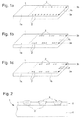
- the photoreceptor integrated circuit 1 is made in a semiconductor substrate, such as a silicon substrate. It comprises in particular a photosensitive region 1a, which comprises several unrepresented photosensitive elements, such as photodiodes, and a processing unit region 1b for processing the electrical signals supplied by the elements of the photosensitive region.
- the photosensitive region 1a is directly juxtaposed to one side of the treatment unit region 1b as shown by the broken lines at Figures 1a, 1b and 1c .
- the area of this photosensitive region 1a may be half of the area of the treatment unit region 1b.
- the region with processing unit 1b comprises all the contact pads 2, 2 'of the photoreceptor circuit according to the invention, which can be electrically connected to the outside. These contact pads can be symmetrically distributed in the processing unit region.
- the contact pads 2 are for example distributed in two rows 3a and 3b at the periphery of two opposite sides of the treatment unit region 1b in the direction of the length of the two juxtaposed regions.
- the number of contact pads 2 of each row is preferably equal.
- the contact pads 2 of each row may be evenly spaced along the entire length of the treatment unit region 1b as shown in FIG. figure 1a . It can be provided for example 18 contact pads of which 9 contact pads 2 by row 3a, 3b.
- the width of each contact pad may be 100 ⁇ m, while the space between each pad of the same row may be 200 ⁇ m.
- contact pads may be provided in the processing unit region as far as they are symmetrically distributed in said region 1b. They may for example be grouped in regularly spaced packets on each opposite side of the processing unit region as shown in FIG. figure 1 b. They may also be arranged offset from each other on both sides of the processing unit region 1b. This symmetry of the arrangement of the ranges may be necessary to ensure a reliable assembly of the photoreceptor circuit on a printed circuit support by a technique called "flip chip" in English terminology.
- some contact pads 2 are distributed in two rows 3a and 3b and grouped in packets of two contact pads 2 for example, which are regularly spaced apart from each other.
- Other contact pads 2 ' for example two contact pads, may be distributed on the side of the processing unit region, opposite to the connecting side of the two regions 1a and 1b. All contact pads 2, 2, 'shown in this figure 1c , are distributed symmetrically with respect to a center line in the length direction of the photoreceptor integrated circuit.
- the photoreceptor integrated circuit 1 may comprise metal bumps 6 made on the contact pads 2 as shown in FIG. figure 2 .
- the contact pads 2 are conventionally formed on the semiconductor substrate 4. Apertures in the final passivation layer 5 deposited on the substrate 4 are provided to give access to each contact pad 2 of the photoreceptor integrated circuit 1.
- Metal bumps 6 are thus made through the openings of the passivation layer 5 from each contact pad 2 to protrude from the upper surface of said passivation layer.
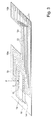
- the figure 3 shows a three-dimensional view of a first embodiment of an optoelectronic component.
- This optoelectronic component comprises on a first face of a substrate 10, which may preferably be flexible, a photoreceptor integrated circuit capable of capturing light generated for example by a not shown light source.
- the photoreceptor circuit therefore comprises a photosensitive region 1a and a treatment unit region 1b according to the embodiment described with reference to FIG. figure 1 for example.
- This photoreceptor circuit is mounted on a first portion 10a of the flexible substrate 10 by a "flip chip” technique.
- contact areas 2 of the photoreceptor circuit which include metal bumps as shown in FIG. figure 2 are electrically connected to corresponding connection pads 12 of the first portion of the substrate 10.
- the connection pads are arranged in the same arrangement and positioning as the metal bumps of the treatment unit region 1b of the circuit in two rows.
- the electrical connection between the metal bumps and the connection pads of the substrate 10 is effected by thermocompression or with the aid of an anisotropic adhesive by applying a force F to the back of the treatment unit 1b region of the photoreceptor circuit. Thanks to the symmetrical arrangement of the contact pads 2 with the metal bumps on the side of the treatment unit region 1b, the contact pressure due to the force F applied to the back of the photoreceptor circuit is distributed uniformly without mechanical stresses on the side. of the photosensitive region 1a. This photosensitive region is thus left free floating on one side of the treatment unit region.
- the flexible substrate 10 further comprises the first portion, a second terminal portion 10b, which carries electrical connection terminals 11, and a connecting portion 10c between the first and second portions 10a and 10b.
- the flexible substrate 10 is in the form of a flexible sheet whose thickness may be of the order of 75 microns.
- Conductive tracks 13, arranged on one side or the other of each portion of the flexible substrate 10, make it possible to connect certain connection pads 12 to the connection terminals 11.
- a through opening 14 is also provided in the first portion 10a facing only of the photosensitive region 1a of the photoreceptor circuit, since said circuit is flip chip-mounted on said substrate.
- the aperture 14 allows the photosensitive region to capture light directly from a light source or by reflection on a work surface.
- a not shown encapsulation of at least the processing unit region 1b may be provided to house this region of the light and to stiffen the first portion of the flexible substrate, while leaving free and without mechanical stresses the photosensitive region 1a. This makes it possible to produce a small optoelectronic component. Moreover thanks to the flexible substrate with a connecting portion 10c, this allows adjustment of the second portion 10b of electrical connection of the component relative to the first portion 10a carrying the photoreceptor circuit.
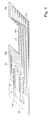
- the figure 4 represents a three-dimensional view of a second embodiment of the optoelectronic component.
- This optoelectronic component comprises a photoreceptor circuit mounted on a first portion 10a of a flexible substrate 10.
- the photoreceptor circuit may be of the embodiment described with reference to FIG. figure 1a for example.
- Said substrate comprises as for the first embodiment, a second portion 10b, which carries electrical connection terminals 11, and a connecting portion 10c between the first and second portions.
- the photoreceptor circuit comprises a photosensitive region 1a and a region with a treatment unit 1b.
- the back of the photoreceptor circuit is fixed on one face of the first portion 10a of the flexible substrate 10.
- the receiving surface of the photosensitive region 1a is therefore opposite to the fixing face of the circuit photoreceptor on the first portion of the substrate 10. As a result, there is no opening through this first portion 10a.
- the first portion 10a of the substrate 10 comprises two rows of connection pads 12 each disposed on two opposite sides of the processing unit region 1b only. These connection pads 12 can be arranged in the same way as the contact pads 2 of the processing unit region 1b.
- the electrical connection of the contact pads 2 is carried out in this second embodiment by metal wires 15, such as aluminum wires, to the corresponding connection pads 12 of the first portion 10a of the substrate 10.
- These connection pads 12 are connected to conductive tracks 13, preferably metal, which are arranged on one side or the other of the substrate. The conductive tracks thus connect the connection pads 12 to the connection terminals 11 placed on the second portion 10b of the substrate.
- Such an optoelectronic component can be used in any type of electronic instrument, such as an optically operating computer mouse.
- the first portion of the substrate with the photoreceptor circuit and possibly a light source circuit, which are protected by a cover, is mounted on a transparent lens block attached to an opening in the bottom of the mouse housing.
- the connection terminals of the second portion of the substrate are connected directly to a motherboard remote from the bottom of the housing inside the mouse.
Landscapes
- Solid State Image Pick-Up Elements (AREA)
- Light Receiving Elements (AREA)
- Structures For Mounting Electric Components On Printed Circuit Boards (AREA)
Applications Claiming Priority (1)
| Application Number | Priority Date | Filing Date | Title |
|---|---|---|---|
| CH4512007 | 2007-03-21 |
Publications (3)
| Publication Number | Publication Date |
|---|---|
| EP1973166A2 true EP1973166A2 (de) | 2008-09-24 |
| EP1973166A3 EP1973166A3 (de) | 2011-05-04 |
| EP1973166B1 EP1973166B1 (de) | 2015-09-09 |
Family
ID=39566895
Family Applications (1)
| Application Number | Title | Priority Date | Filing Date |
|---|---|---|---|
| EP08151943.1A Active EP1973166B1 (de) | 2007-03-21 | 2008-02-26 | Integrierter Photorezeptorschaltkreis und diesen umfassende optoelektronische Komponente |
Country Status (4)
| Country | Link |
|---|---|
| US (1) | US7579579B2 (de) |
| EP (1) | EP1973166B1 (de) |
| CN (1) | CN101271906B (de) |
| TW (1) | TWI449182B (de) |
Families Citing this family (1)
| Publication number | Priority date | Publication date | Assignee | Title |
|---|---|---|---|---|
| CN107819981A (zh) * | 2017-09-27 | 2018-03-20 | 京东方科技集团股份有限公司 | 成像背板、成像装置及电子设备 |
Family Cites Families (13)
| Publication number | Priority date | Publication date | Assignee | Title |
|---|---|---|---|---|
| JPS5136343B2 (de) * | 1972-05-26 | 1976-10-07 | ||
| JPS5846071B2 (ja) | 1979-06-28 | 1983-10-14 | 横河電機株式会社 | 半導体集積装置 |
| JPH0697510A (ja) | 1992-09-11 | 1994-04-08 | Toshiba Corp | 小型光半導体装置 |
| US5865935A (en) * | 1995-02-02 | 1999-02-02 | Eastman Kodak Company | Method of packaging image sensors |
| JP3320335B2 (ja) * | 1997-05-30 | 2002-09-03 | キヤノン株式会社 | 光電変換装置及び密着型イメージセンサ |
| JP4192335B2 (ja) * | 1999-05-24 | 2008-12-10 | 株式会社デンソー | 光センサic及びその検査方法 |
| US7583309B2 (en) * | 2002-06-28 | 2009-09-01 | Kyocera Coproration | Imaging device package camera module and camera module producing method |
| TWI225696B (en) * | 2003-06-10 | 2004-12-21 | Advanced Semiconductor Eng | Semiconductor package and method for manufacturing the same |
| JP4542768B2 (ja) * | 2003-11-25 | 2010-09-15 | 富士フイルム株式会社 | 固体撮像装置及びその製造方法 |
| TWI244174B (en) * | 2003-12-31 | 2005-11-21 | Siliconware Precision Industries Co Ltd | Photosensitive semiconductor package and method for fabricating the same |
| JP3857694B2 (ja) | 2004-02-05 | 2006-12-13 | ローム株式会社 | 光通信モジュール |
| CN2760758Y (zh) * | 2004-12-16 | 2006-02-22 | 力捷电脑(中国)有限公司 | Cmos图像传感器芯片软板连接结构 |
| DE102005002352A1 (de) | 2005-01-18 | 2006-07-27 | Vishay Semiconductor Gmbh | Infrarot-Transceiver und Herstellungsverfahren |
-
2008
- 2008-02-26 EP EP08151943.1A patent/EP1973166B1/de active Active
- 2008-03-06 US US12/043,303 patent/US7579579B2/en active Active
- 2008-03-18 TW TW097109525A patent/TWI449182B/zh active
- 2008-03-19 CN CN200810086834.3A patent/CN101271906B/zh active Active
Also Published As
| Publication number | Publication date |
|---|---|
| TWI449182B (zh) | 2014-08-11 |
| US7579579B2 (en) | 2009-08-25 |
| EP1973166A3 (de) | 2011-05-04 |
| TW200903815A (en) | 2009-01-16 |
| US20080230679A1 (en) | 2008-09-25 |
| EP1973166B1 (de) | 2015-09-09 |
| CN101271906B (zh) | 2012-10-31 |
| CN101271906A (zh) | 2008-09-24 |
Similar Documents
| Publication | Publication Date | Title |
|---|---|---|
| KR101453158B1 (ko) | 이미지 센서를 위한 계단형 패키지 및 그 제조 방법 | |
| CN103681715B (zh) | 低轮廓图像传感器封装和方法 | |
| US7453509B2 (en) | Digital camera with a transparent core disposed between a lens and a light-sensitive sensor | |
| FR2700416A1 (fr) | Dispositif à semiconducteurs comportant un élément semiconducteur sur un élément de montage. | |
| CN103311256A (zh) | 改进的背面照明图像传感器架构及其制造方法 | |
| EP1962173B1 (de) | Optoelektronisches Modul, das mit mindestens einem Fotorezeptor-Schaltkreis ausgestattet ist | |
| EP0702850A1 (de) | Hybride halbleiteranordnung | |
| CN111758165A (zh) | 固态摄像装置和固态摄像器件 | |
| EP2031714A1 (de) | Optoelektronischer Schaltkreis mit einem Photoempfänger und einer Laserdiode und diesen umfassendes Modul | |
| JPWO2020039733A1 (ja) | 半導体装置、電子機器、および半導体装置の製造方法 | |
| EP3894813B1 (de) | Verfahren zur herstellung eines infrarotdetektors und zugehöriger infrarotdetektor | |
| FR2952473A1 (fr) | Procede de realisation d'un circuit courbe | |
| FR3060851A1 (fr) | Module optoelectronique 3d d'imagerie | |
| EP1973166B1 (de) | Integrierter Photorezeptorschaltkreis und diesen umfassende optoelektronische Komponente | |
| CN101983430B (zh) | 具有载体基板和再分配层的背面受光成像传感器 | |
| CN108886066B (zh) | 半导体受光模块及半导体受光模块的制造方法 | |
| EP2533519B1 (de) | Infrarot-Abbildungsvorrichtung mit integrierter Abschirmung gegen Infrarot-Störstrahlung und Verfahren zum Herstellen der Vorrichtung | |
| FR2922682A1 (fr) | Procede de fabrication d'un micromodule de capture d'images | |
| CA2915853A1 (fr) | Capteur differentiel de temperature | |
| JPH09246420A (ja) | 半導体装置及びその製法 | |
| CN116490967A (zh) | 成像装置、电子设备和成像装置的制造方法 | |
| FR2794287A1 (fr) | Detecteur a semi-conducteur pour la detection de rayonnements ionisants | |
| EP4268281B1 (de) | Integration einer detektionsschaltung auf der basis von optischen resonatoren, die mit einer ausleseschaltung eines bildaufnehmers verbunden sind | |
| JP2024098542A (ja) | 撮像装置、電子機器 | |
| EP0948059A1 (de) | Positionierungsmittel in einem mikroelektronischen Bauelement und Bildsensor mit Verwendung dieses Bauelements |
Legal Events
| Date | Code | Title | Description |
|---|---|---|---|
| PUAI | Public reference made under article 153(3) epc to a published international application that has entered the european phase |
Free format text: ORIGINAL CODE: 0009012 |
|
| AK | Designated contracting states |
Kind code of ref document: A2 Designated state(s): AT BE BG CH CY CZ DE DK EE ES FI FR GB GR HR HU IE IS IT LI LT LU LV MC MT NL NO PL PT RO SE SI SK TR |
|
| AX | Request for extension of the european patent |
Extension state: AL BA MK RS |
|
| PUAL | Search report despatched |
Free format text: ORIGINAL CODE: 0009013 |
|
| AK | Designated contracting states |
Kind code of ref document: A3 Designated state(s): AT BE BG CH CY CZ DE DK EE ES FI FR GB GR HR HU IE IS IT LI LT LU LV MC MT NL NO PL PT RO SE SI SK TR |
|
| AX | Request for extension of the european patent |
Extension state: AL BA MK RS |
|
| RIC1 | Information provided on ipc code assigned before grant |
Ipc: H01L 31/0224 20060101AFI20080716BHEP Ipc: H01L 27/146 20060101ALI20110325BHEP |
|
| 17P | Request for examination filed |
Effective date: 20111104 |
|
| AKX | Designation fees paid |
Designated state(s): AT BE BG CH CY CZ DE DK EE ES FI FR GB GR HR HU IE IS IT LI LT LU LV MC MT NL NO PL PT RO SE SI SK TR |
|
| 17Q | First examination report despatched |
Effective date: 20111216 |
|
| REG | Reference to a national code |
Ref country code: DE Ref legal event code: R079 Ref document number: 602008040041 Country of ref document: DE Free format text: PREVIOUS MAIN CLASS: H01L0031022400 Ipc: H01L0027144000 |
|
| RIC1 | Information provided on ipc code assigned before grant |
Ipc: H01L 31/0224 20060101ALI20150319BHEP Ipc: H01L 27/146 20060101ALI20150319BHEP Ipc: H01L 27/144 20060101AFI20150319BHEP |
|
| GRAP | Despatch of communication of intention to grant a patent |
Free format text: ORIGINAL CODE: EPIDOSNIGR1 |
|
| INTG | Intention to grant announced |
Effective date: 20150611 |
|
| GRAS | Grant fee paid |
Free format text: ORIGINAL CODE: EPIDOSNIGR3 |
|
| GRAA | (expected) grant |
Free format text: ORIGINAL CODE: 0009210 |
|
| AK | Designated contracting states |
Kind code of ref document: B1 Designated state(s): AT BE BG CH CY CZ DE DK EE ES FI FR GB GR HR HU IE IS IT LI LT LU LV MC MT NL NO PL PT RO SE SI SK TR |
|
| REG | Reference to a national code |
Ref country code: GB Ref legal event code: FG4D Free format text: NOT ENGLISH |
|
| REG | Reference to a national code |
Ref country code: AT Ref legal event code: REF Ref document number: 748742 Country of ref document: AT Kind code of ref document: T Effective date: 20150915 Ref country code: CH Ref legal event code: EP |
|
| REG | Reference to a national code |
Ref country code: IE Ref legal event code: FG4D Free format text: LANGUAGE OF EP DOCUMENT: FRENCH |
|
| REG | Reference to a national code |
Ref country code: DE Ref legal event code: R096 Ref document number: 602008040041 Country of ref document: DE |
|
| REG | Reference to a national code |
Ref country code: NL Ref legal event code: MP Effective date: 20150909 |
|
| REG | Reference to a national code |
Ref country code: FR Ref legal event code: PLFP Year of fee payment: 9 |
|
| PG25 | Lapsed in a contracting state [announced via postgrant information from national office to epo] |
Ref country code: LT Free format text: LAPSE BECAUSE OF FAILURE TO SUBMIT A TRANSLATION OF THE DESCRIPTION OR TO PAY THE FEE WITHIN THE PRESCRIBED TIME-LIMIT Effective date: 20150909 Ref country code: GR Free format text: LAPSE BECAUSE OF FAILURE TO SUBMIT A TRANSLATION OF THE DESCRIPTION OR TO PAY THE FEE WITHIN THE PRESCRIBED TIME-LIMIT Effective date: 20151210 Ref country code: NO Free format text: LAPSE BECAUSE OF FAILURE TO SUBMIT A TRANSLATION OF THE DESCRIPTION OR TO PAY THE FEE WITHIN THE PRESCRIBED TIME-LIMIT Effective date: 20151209 Ref country code: LV Free format text: LAPSE BECAUSE OF FAILURE TO SUBMIT A TRANSLATION OF THE DESCRIPTION OR TO PAY THE FEE WITHIN THE PRESCRIBED TIME-LIMIT Effective date: 20150909 Ref country code: FI Free format text: LAPSE BECAUSE OF FAILURE TO SUBMIT A TRANSLATION OF THE DESCRIPTION OR TO PAY THE FEE WITHIN THE PRESCRIBED TIME-LIMIT Effective date: 20150909 |
|
| REG | Reference to a national code |
Ref country code: LT Ref legal event code: MG4D |
|
| REG | Reference to a national code |
Ref country code: AT Ref legal event code: MK05 Ref document number: 748742 Country of ref document: AT Kind code of ref document: T Effective date: 20150909 |
|
| PG25 | Lapsed in a contracting state [announced via postgrant information from national office to epo] |
Ref country code: ES Free format text: LAPSE BECAUSE OF FAILURE TO SUBMIT A TRANSLATION OF THE DESCRIPTION OR TO PAY THE FEE WITHIN THE PRESCRIBED TIME-LIMIT Effective date: 20150909 Ref country code: HR Free format text: LAPSE BECAUSE OF FAILURE TO SUBMIT A TRANSLATION OF THE DESCRIPTION OR TO PAY THE FEE WITHIN THE PRESCRIBED TIME-LIMIT Effective date: 20150909 Ref country code: SE Free format text: LAPSE BECAUSE OF FAILURE TO SUBMIT A TRANSLATION OF THE DESCRIPTION OR TO PAY THE FEE WITHIN THE PRESCRIBED TIME-LIMIT Effective date: 20150909 |
|
| PG25 | Lapsed in a contracting state [announced via postgrant information from national office to epo] |
Ref country code: NL Free format text: LAPSE BECAUSE OF FAILURE TO SUBMIT A TRANSLATION OF THE DESCRIPTION OR TO PAY THE FEE WITHIN THE PRESCRIBED TIME-LIMIT Effective date: 20150909 |
|
| PG25 | Lapsed in a contracting state [announced via postgrant information from national office to epo] |
Ref country code: IS Free format text: LAPSE BECAUSE OF FAILURE TO SUBMIT A TRANSLATION OF THE DESCRIPTION OR TO PAY THE FEE WITHIN THE PRESCRIBED TIME-LIMIT Effective date: 20160109 Ref country code: IT Free format text: LAPSE BECAUSE OF FAILURE TO SUBMIT A TRANSLATION OF THE DESCRIPTION OR TO PAY THE FEE WITHIN THE PRESCRIBED TIME-LIMIT Effective date: 20150909 Ref country code: SK Free format text: LAPSE BECAUSE OF FAILURE TO SUBMIT A TRANSLATION OF THE DESCRIPTION OR TO PAY THE FEE WITHIN THE PRESCRIBED TIME-LIMIT Effective date: 20150909 Ref country code: CZ Free format text: LAPSE BECAUSE OF FAILURE TO SUBMIT A TRANSLATION OF THE DESCRIPTION OR TO PAY THE FEE WITHIN THE PRESCRIBED TIME-LIMIT Effective date: 20150909 Ref country code: EE Free format text: LAPSE BECAUSE OF FAILURE TO SUBMIT A TRANSLATION OF THE DESCRIPTION OR TO PAY THE FEE WITHIN THE PRESCRIBED TIME-LIMIT Effective date: 20150909 |
|
| PG25 | Lapsed in a contracting state [announced via postgrant information from national office to epo] |
Ref country code: BE Free format text: LAPSE BECAUSE OF NON-PAYMENT OF DUE FEES Effective date: 20160229 Ref country code: PL Free format text: LAPSE BECAUSE OF FAILURE TO SUBMIT A TRANSLATION OF THE DESCRIPTION OR TO PAY THE FEE WITHIN THE PRESCRIBED TIME-LIMIT Effective date: 20150909 Ref country code: PT Free format text: LAPSE BECAUSE OF FAILURE TO SUBMIT A TRANSLATION OF THE DESCRIPTION OR TO PAY THE FEE WITHIN THE PRESCRIBED TIME-LIMIT Effective date: 20160111 Ref country code: AT Free format text: LAPSE BECAUSE OF FAILURE TO SUBMIT A TRANSLATION OF THE DESCRIPTION OR TO PAY THE FEE WITHIN THE PRESCRIBED TIME-LIMIT Effective date: 20150909 Ref country code: RO Free format text: LAPSE BECAUSE OF FAILURE TO SUBMIT A TRANSLATION OF THE DESCRIPTION OR TO PAY THE FEE WITHIN THE PRESCRIBED TIME-LIMIT Effective date: 20150909 |
|
| REG | Reference to a national code |
Ref country code: DE Ref legal event code: R097 Ref document number: 602008040041 Country of ref document: DE |
|
| PLBE | No opposition filed within time limit |
Free format text: ORIGINAL CODE: 0009261 |
|
| STAA | Information on the status of an ep patent application or granted ep patent |
Free format text: STATUS: NO OPPOSITION FILED WITHIN TIME LIMIT |
|
| 26N | No opposition filed |
Effective date: 20160610 |
|
| PG25 | Lapsed in a contracting state [announced via postgrant information from national office to epo] |
Ref country code: DK Free format text: LAPSE BECAUSE OF FAILURE TO SUBMIT A TRANSLATION OF THE DESCRIPTION OR TO PAY THE FEE WITHIN THE PRESCRIBED TIME-LIMIT Effective date: 20150909 Ref country code: SI Free format text: LAPSE BECAUSE OF FAILURE TO SUBMIT A TRANSLATION OF THE DESCRIPTION OR TO PAY THE FEE WITHIN THE PRESCRIBED TIME-LIMIT Effective date: 20150909 |
|
| PG25 | Lapsed in a contracting state [announced via postgrant information from national office to epo] |
Ref country code: LU Free format text: LAPSE BECAUSE OF FAILURE TO SUBMIT A TRANSLATION OF THE DESCRIPTION OR TO PAY THE FEE WITHIN THE PRESCRIBED TIME-LIMIT Effective date: 20160226 Ref country code: MC Free format text: LAPSE BECAUSE OF FAILURE TO SUBMIT A TRANSLATION OF THE DESCRIPTION OR TO PAY THE FEE WITHIN THE PRESCRIBED TIME-LIMIT Effective date: 20150909 |
|
| REG | Reference to a national code |
Ref country code: CH Ref legal event code: PL |
|
| GBPC | Gb: european patent ceased through non-payment of renewal fee |
Effective date: 20160226 |
|
| PG25 | Lapsed in a contracting state [announced via postgrant information from national office to epo] |
Ref country code: CH Free format text: LAPSE BECAUSE OF NON-PAYMENT OF DUE FEES Effective date: 20160229 Ref country code: LI Free format text: LAPSE BECAUSE OF NON-PAYMENT OF DUE FEES Effective date: 20160229 |
|
| REG | Reference to a national code |
Ref country code: IE Ref legal event code: MM4A |
|
| REG | Reference to a national code |
Ref country code: FR Ref legal event code: PLFP Year of fee payment: 10 |
|
| PG25 | Lapsed in a contracting state [announced via postgrant information from national office to epo] |
Ref country code: GB Free format text: LAPSE BECAUSE OF NON-PAYMENT OF DUE FEES Effective date: 20160226 Ref country code: IE Free format text: LAPSE BECAUSE OF NON-PAYMENT OF DUE FEES Effective date: 20160226 |
|
| PG25 | Lapsed in a contracting state [announced via postgrant information from national office to epo] |
Ref country code: MT Free format text: LAPSE BECAUSE OF FAILURE TO SUBMIT A TRANSLATION OF THE DESCRIPTION OR TO PAY THE FEE WITHIN THE PRESCRIBED TIME-LIMIT Effective date: 20150909 |
|
| REG | Reference to a national code |
Ref country code: FR Ref legal event code: PLFP Year of fee payment: 11 |
|
| PG25 | Lapsed in a contracting state [announced via postgrant information from national office to epo] |
Ref country code: CY Free format text: LAPSE BECAUSE OF FAILURE TO SUBMIT A TRANSLATION OF THE DESCRIPTION OR TO PAY THE FEE WITHIN THE PRESCRIBED TIME-LIMIT Effective date: 20150909 Ref country code: HU Free format text: LAPSE BECAUSE OF FAILURE TO SUBMIT A TRANSLATION OF THE DESCRIPTION OR TO PAY THE FEE WITHIN THE PRESCRIBED TIME-LIMIT; INVALID AB INITIO Effective date: 20080226 |
|
| PG25 | Lapsed in a contracting state [announced via postgrant information from national office to epo] |
Ref country code: TR Free format text: LAPSE BECAUSE OF FAILURE TO SUBMIT A TRANSLATION OF THE DESCRIPTION OR TO PAY THE FEE WITHIN THE PRESCRIBED TIME-LIMIT Effective date: 20150909 |
|
| PG25 | Lapsed in a contracting state [announced via postgrant information from national office to epo] |
Ref country code: BG Free format text: LAPSE BECAUSE OF FAILURE TO SUBMIT A TRANSLATION OF THE DESCRIPTION OR TO PAY THE FEE WITHIN THE PRESCRIBED TIME-LIMIT Effective date: 20150909 |
|
| P01 | Opt-out of the competence of the unified patent court (upc) registered |
Effective date: 20230611 |
|
| PGFP | Annual fee paid to national office [announced via postgrant information from national office to epo] |
Ref country code: DE Payment date: 20240123 Year of fee payment: 17 |
|
| REG | Reference to a national code |
Ref country code: DE Ref legal event code: R079 Ref document number: 602008040041 Country of ref document: DE Free format text: PREVIOUS MAIN CLASS: H01L0027144000 Ipc: H10F0039100000 |
|
| PGFP | Annual fee paid to national office [announced via postgrant information from national office to epo] |
Ref country code: FR Payment date: 20250122 Year of fee payment: 18 |
|
| REG | Reference to a national code |
Ref country code: DE Ref legal event code: R119 Ref document number: 602008040041 Country of ref document: DE |
|
| PG25 | Lapsed in a contracting state [announced via postgrant information from national office to epo] |
Ref country code: DE Free format text: LAPSE BECAUSE OF NON-PAYMENT OF DUE FEES Effective date: 20250902 |