EP1973158B1 - Elektronisches Bauteil - Google Patents
Elektronisches Bauteil Download PDFInfo
- Publication number
- EP1973158B1 EP1973158B1 EP07006090.0A EP07006090A EP1973158B1 EP 1973158 B1 EP1973158 B1 EP 1973158B1 EP 07006090 A EP07006090 A EP 07006090A EP 1973158 B1 EP1973158 B1 EP 1973158B1
- Authority
- EP
- European Patent Office
- Prior art keywords
- conductor foil
- semiconductor element
- bump
- contact
- electronic component
- Prior art date
- Legal status (The legal status is an assumption and is not a legal conclusion. Google has not performed a legal analysis and makes no representation as to the accuracy of the status listed.)
- Not-in-force
Links
Images
Classifications
-
- H—ELECTRICITY
- H01—ELECTRIC ELEMENTS
- H01L—SEMICONDUCTOR DEVICES NOT COVERED BY CLASS H10
- H01L23/00—Details of semiconductor or other solid state devices
- H01L23/48—Arrangements for conducting electric current to or from the solid state body in operation, e.g. leads, terminal arrangements ; Selection of materials therefor
- H01L23/488—Arrangements for conducting electric current to or from the solid state body in operation, e.g. leads, terminal arrangements ; Selection of materials therefor consisting of soldered or bonded constructions
- H01L23/498—Leads, i.e. metallisations or lead-frames on insulating substrates, e.g. chip carriers
- H01L23/4985—Flexible insulating substrates
-
- H—ELECTRICITY
- H01—ELECTRIC ELEMENTS
- H01L—SEMICONDUCTOR DEVICES NOT COVERED BY CLASS H10
- H01L23/00—Details of semiconductor or other solid state devices
- H01L23/12—Mountings, e.g. non-detachable insulating substrates
- H01L23/13—Mountings, e.g. non-detachable insulating substrates characterised by the shape
-
- H—ELECTRICITY
- H05—ELECTRIC TECHNIQUES NOT OTHERWISE PROVIDED FOR
- H05K—PRINTED CIRCUITS; CASINGS OR CONSTRUCTIONAL DETAILS OF ELECTRIC APPARATUS; MANUFACTURE OF ASSEMBLAGES OF ELECTRICAL COMPONENTS
- H05K3/00—Apparatus or processes for manufacturing printed circuits
- H05K3/40—Forming printed elements for providing electric connections to or between printed circuits
- H05K3/4007—Surface contacts, e.g. bumps
-
- H—ELECTRICITY
- H01—ELECTRIC ELEMENTS
- H01L—SEMICONDUCTOR DEVICES NOT COVERED BY CLASS H10
- H01L2924/00—Indexing scheme for arrangements or methods for connecting or disconnecting semiconductor or solid-state bodies as covered by H01L24/00
- H01L2924/0001—Technical content checked by a classifier
- H01L2924/0002—Not covered by any one of groups H01L24/00, H01L24/00 and H01L2224/00
-
- H—ELECTRICITY
- H05—ELECTRIC TECHNIQUES NOT OTHERWISE PROVIDED FOR
- H05K—PRINTED CIRCUITS; CASINGS OR CONSTRUCTIONAL DETAILS OF ELECTRIC APPARATUS; MANUFACTURE OF ASSEMBLAGES OF ELECTRICAL COMPONENTS
- H05K1/00—Printed circuits
- H05K1/02—Details
- H05K1/11—Printed elements for providing electric connections to or between printed circuits
- H05K1/111—Pads for surface mounting, e.g. lay-out
-
- H—ELECTRICITY
- H05—ELECTRIC TECHNIQUES NOT OTHERWISE PROVIDED FOR
- H05K—PRINTED CIRCUITS; CASINGS OR CONSTRUCTIONAL DETAILS OF ELECTRIC APPARATUS; MANUFACTURE OF ASSEMBLAGES OF ELECTRICAL COMPONENTS
- H05K1/00—Printed circuits
- H05K1/18—Printed circuits structurally associated with non-printed electric components
- H05K1/189—Printed circuits structurally associated with non-printed electric components characterised by the use of a flexible or folded printed circuit
-
- H—ELECTRICITY
- H05—ELECTRIC TECHNIQUES NOT OTHERWISE PROVIDED FOR
- H05K—PRINTED CIRCUITS; CASINGS OR CONSTRUCTIONAL DETAILS OF ELECTRIC APPARATUS; MANUFACTURE OF ASSEMBLAGES OF ELECTRICAL COMPONENTS
- H05K2201/00—Indexing scheme relating to printed circuits covered by H05K1/00
- H05K2201/03—Conductive materials
- H05K2201/0332—Structure of the conductor
- H05K2201/0364—Conductor shape
- H05K2201/0367—Metallic bump or raised conductor not used as solder bump
-
- H—ELECTRICITY
- H05—ELECTRIC TECHNIQUES NOT OTHERWISE PROVIDED FOR
- H05K—PRINTED CIRCUITS; CASINGS OR CONSTRUCTIONAL DETAILS OF ELECTRIC APPARATUS; MANUFACTURE OF ASSEMBLAGES OF ELECTRICAL COMPONENTS
- H05K2201/00—Indexing scheme relating to printed circuits covered by H05K1/00
- H05K2201/09—Shape and layout
- H05K2201/09009—Substrate related
- H05K2201/091—Locally and permanently deformed areas including dielectric material
-
- H—ELECTRICITY
- H05—ELECTRIC TECHNIQUES NOT OTHERWISE PROVIDED FOR
- H05K—PRINTED CIRCUITS; CASINGS OR CONSTRUCTIONAL DETAILS OF ELECTRIC APPARATUS; MANUFACTURE OF ASSEMBLAGES OF ELECTRICAL COMPONENTS
- H05K2201/00—Indexing scheme relating to printed circuits covered by H05K1/00
- H05K2201/10—Details of components or other objects attached to or integrated in a printed circuit board
- H05K2201/10613—Details of electrical connections of non-printed components, e.g. special leads
- H05K2201/10621—Components characterised by their electrical contacts
- H05K2201/10674—Flip chip
-
- H—ELECTRICITY
- H05—ELECTRIC TECHNIQUES NOT OTHERWISE PROVIDED FOR
- H05K—PRINTED CIRCUITS; CASINGS OR CONSTRUCTIONAL DETAILS OF ELECTRIC APPARATUS; MANUFACTURE OF ASSEMBLAGES OF ELECTRICAL COMPONENTS
- H05K3/00—Apparatus or processes for manufacturing printed circuits
- H05K3/30—Assembling printed circuits with electric components, e.g. with resistor
- H05K3/32—Assembling printed circuits with electric components, e.g. with resistor electrically connecting electric components or wires to printed circuits
- H05K3/321—Assembling printed circuits with electric components, e.g. with resistor electrically connecting electric components or wires to printed circuits by conductive adhesives
Definitions
- the invention relates to an electronic component having a semiconductor element and at least one contact element attached to one side of the semiconductor element.
- a contacting by wire bonding requires considerable space, since the wires must be guided in an arc from the top of the semiconductor to the substrate.
- the connecting wires can not be performed arbitrarily, since the wires must not touch even with vibrations of the component. As a result, the production of complex interconnected modules is made more difficult. This method is also relatively expensive.
- the flip-chip assembly is indeed cheaper.
- the solder balls described above must be on the substrate and / or the semiconductor device, which requires a series of preparatory production steps.
- An electronic component according to the preamble of claim 1 is also known from US 2002/0030276 A1 out.
- the US 5,097,101A is concerned with a flexible substrate having at least one conductor track, which has at least one bump, which forms a local elevation with respect to a plane of the substrate and which is positioned and dimensioned such that at least a portion of the conductor track of the substrate runs on the bump. Further, the cited document discloses a method of making the bump in the substrate by embossing.
- the DE 102 35 208 A1 describes a contact element consisting of a substrate provided with at least one localized projection and an electrically conductive coating located on the substrate and also on the projection.
- the cited document also describes a method for producing such a contact element by means of an embossing process.
- the US 2005/0237365 A1 describes an actuator with at least one contact element attached to one side of the actuator, wherein the contact element comprises a flexible conductor foil with at least one conductor track.
- the conductor foil has a bump which forms a local elevation with respect to a plane of the conductor foil and which is positioned and dimensioned such that at least a portion of the conductor path of the conductor foil extends on the bump, the conductor portion being in electrical contact with at least one contact point of the actuator stands.
- the cited document describes to produce contact bumps in the contact element by embossing.
- the US Pat. No. 6,881,611 B1 discloses an electronic component having a semiconductor element and at least one contact element fastened to one side of the semiconductor element, wherein the contact element comprises a flexible conductor foil with at least one conductor track.
- the conductor foil has a bump which forms a local elevation with respect to a plane of the conductor foil and which is positioned and dimensioned such that at least a portion of the conductor track of the conductor foil extends on the bump.
- the US 2004/0227256 A1 also relates to an electronic component having a semiconductor element and at least one contact element fastened to one side of the semiconductor element, wherein the contact element comprises a flexible conductor foil with at least one conductor track.
- the conductor foil has a bump which forms a local elevation with respect to a plane of the conductor foil and which is positioned and dimensioned such that at least a portion of the conductor path of the conductor foil extends on the bump, the conductor portion being in electrical contact with at least one contact point of the semiconductor element stands.
- the invention is therefore based on the object to provide a compact electronic component with a contact element, which is inexpensive to manufacture and at the same time is flexible, so that it can be used in a variety of different circuits.
- the electronic component according to the invention has a semiconductor element and at least one contact element fastened to one side of the semiconductor element.
- the contact element comprises a flexible conductor foil with at least one conductor track. With substantially constant conductor foil thickness, the conductor foil has at least one protuberance which forms a local elevation with respect to a conductor foil plane.
- the bump is positioned and dimensioned such that at least a portion of the conductor track of the conductor foil runs on the bump.
- the conductor track section is in electrical contact with at least one contact point of the semiconductor element.
- the semiconductor element is connected to a flexible contact foil which has bumps or protrusions which rise from a conductor foil plane.
- these surveys are not local thickening of the conductor foil.
- the conductor foil has substantially the same thickness in the area of the protuberance as in the other areas.
- the conductor track section can end on the hump.
- the conductor track section lies on the bump in a plane above the conductor foil plane-thus projects out of it-and can be contacted in a simple manner with the contact point of the semiconductor.
- a corresponding bump can be easily formed in the flexible conductor foil.
- the contacting of the conductor foil with the semiconductor element also poses no problem, since the spatial arrangement and expansion of the hump is adapted to the arrangement and extent of the contact point of the semiconductor element.
- the conductor foil has a plurality of bumps and conductor tracks, so that even complex connections of a semiconductor element comprising a plurality of contact points can be realized.
- the contacting of the various bumps with the contact points of the semiconductor element - in contrast to a contacting by means of wires - in one step.
- the use of a flexible conductor foil as a contact element also offers the possibility to connect the semiconductor element in a variable manner with other components, since the flexible conductor foil - unlike rigid printed circuit boards - allows within a certain frame relative movements between different components of an electronic circuit in which the invention electronic component is integrated.
- the contact element may have, in addition to the at least one bump in its course, at least in sections, several bends and / or bends. These bends / bends can be provided in particular in the course of the contact element, which is located outside a contacting region of the conductor foil.
- the contacting region is the region of the conductor foil which has the bumps and therefore for contacting and fixing the conductor foil to the semiconductor element is provided.
- bends / bends can also be provided in electronic components which are connected by means of conventional contacting methods with a conductor foil without a bump.
- bends for example, effects of a thermal expansion of the components of a circuit can be compensated, which is usually not possible with the use of substantially rigid circuit boards-or only with great effort.
- the bends and / or bends may, for example, form a wave-like or accordion-like section in the course of the conductor foil.
- the bumps may be formed in various ways and, for example, have a substantially dome-shaped, U-shaped, rectangular or triangular cross-section in a plane perpendicular to the conductor foil plane.
- the dimensioning of the bumps in a conductor foil plane i. the area occupied by them can also be adapted to the specific needs.
- square, rectangular, circular and oval bumps may be mentioned at this point, although more complex forms can also be realized.
- the conductor foil is provided with a plurality of bumps, which have different cross sections and / or which are dimensioned differently. In other words, different types of bumps can be combined to ensure an optimal connection of the semiconductor element to the conductor tracks of the conductor foil.
- the bumps while a substantially same height - wherein the "height" of the distance between a Vertex of the hump and the conductor foil level to understand is - have.
- the bumps may also have different heights or height profiles.
- a side of the semiconductor element facing away from the conductor foil having the bump is connected to a substrate or a cooling element.
- the conductor track section running on the bump can be electrically conductively connected to the contact point of the semiconductor element by means of a conductive adhesive. It is possible to use isotropic or anisotropic conductive adhesives. It can also be provided to solder the contact point of the semiconductor element to the conductor track section running on the bump. The choice of the type of connection depends inter alia on the size of the contact points and the required properties of the electronic component.
- the conductor track section running on the bump comprises a contact surface, which is wider in the conductor foil plane in a longitudinal extension direction of the conductor track than the conductor track, and which is connectable to the contact point of the semiconductor element. This simplifies the contacting of the conductor track with the contact point of the semiconductor element.
- the conductor runs on the hump in the contact surface and ends there.
- the thickness of the conductor foil is about 0.4 to 2 mm.
- Such a conductor foil allows easy shaping of the bumps and / or bends and / or curves and has sufficient flexibility to use the electronic component in a variety of ways.
- the invention further relates to an electronic circuit comprising at least two electronic components according to one of the embodiments described above, wherein the electronic components have a common contact element.
- the electronic components of the electronic circuit are connected to one and the same conductor foil.
- the invention comprises a method for producing an electronic component.
- a semiconductor element and a flexible, substantially planar conductor foil with at least one conductor track are provided.
- the conductor foil is introduced into a region between die halves of a machine for embossing the conductor foil. Subsequently, the die halves are closed and the conductor foil is subjected to an increased pressure, whereby the conductor foil is deformed. Subsequently, the pressure is reduced again. The die halves are opened and the embossed conductor foil is removed.
- the semiconductor element is contacted with the conductor foil in such a way that at least one contact point of the semiconductor element is brought into contact with the conductor track, which runs at least in sections on at least one bump which has been embossed by the die halves into the conductor foil.
- the die halves are preheated to a working temperature prior to introducing the conductor foil.
- the temperature of the die halves is substantially equal to the working temperature.
- the die halves are cooled.
- the first phase thus serves the thermoplastic deformation of the conductor foil.
- the pressure during the first and second phases of the pressurization is substantially equal and constant, d. H. the applied pressure does not substantially change during pressurization.
- the working temperature is in a range of about 50 to 200 ° C. This temperature range has proven to be particularly suitable for the deformation of the conductor foil.
- the first phase of the pressurization comprises a duration of about 1 to 10 seconds.
- the second phase of the pressurization comprises a duration of about 1 to 5 seconds.
- the semiconductor element and the conductor foil are electrically conductively connected to one another with the aid of a conductive adhesive or by soldering.
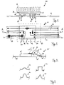
- Fig. 1 shows an electronic component 10, which has a semiconductor element 12 and a conductor foil 14, which forms the contact element of the electronic component.
- the conductor foil 14 may be based on a number of different plastics, for example PEN, PET, PETF, GHE, PI or PEEK.
- the semiconductor element 12 has a contact side 16, on which a plurality of contact points 18 is arranged, which is used for contacting the semiconductor element 12 - which in particular may be an unhoused semiconductor component (s).
- the side of the semiconductor element 12 opposite the contact side 16 forms a mounting side 20.
- a substrate 22, which in turn is connected to a cooling element 24, is fastened to the mounting side 20.
- the mounting side 20 thus serves to mount the cooling element 24 and allows efficient removal of the heat generated during operation of the semiconductor element 12 waste heat.
- the side of the semiconductor element 12 referred to here as the mounting side 20 may also have contact points 18 which provide additional contacting possibilities.
- the contact points 18 of the contact side 16 are connected to bumps 26, which form locally limited elevations in the course of the conductor foil 14. It can be seen that the bumps 26 are integral components of the conductor foil 14. They are not formed by additionally applied material or thickened areas in the course of the conductor foil 12.
- the region of the conductor foil provided with the bumps 26 is referred to as the contacting region K, and is in Fig. 1 marked by two vertical lines, each with an arrow.
- the contacting region K essentially corresponds to the vertical projection of the semiconductor element 12 onto the conductor foil 14.
- connection of the conductor foil 14 with the semiconductor element 12 and the conductor track portions on the protuberances 26 with the contact points 18 can be different Be made way.
- the contacting can be carried out in particular by means of isotropic or anisotropic conductive adhesive (not shown) and / or soldering (soldering joints not shown).
- Fig. 2 shows a view of the contact side 16 of the semiconductor element 12, wherein the conductor foil 14 is shown transparent in order to describe further features of the component 10 according to the invention can.
- the contacting region K in this view essentially coincides with the outline of the semiconductor element 12.
- the position of the in Fig. 1 shown section through the electronic component 10 is indicated by the section line AA '.
- the conductor foil 14 comprises a plurality of conductor tracks 28. At the left and the right end of the conductor foil 14, the conductor tracks 28 terminate in contact surfaces 30, which make it possible to contact the conductor foil 14 with further components of a circuit (not shown).
- the contact surfaces 30 may be of different shapes (eg, square, rectangular, circular, or oval) and of any size.
- contact surfaces 31 are provided, which may also have different shapes and sizes.
- the contact surfaces 31 are at least partially on the bumps 26th
- the contact surfaces 31 are larger than the contact points 18 of the semiconductor element 12, so that the contact points 18 are covered in this view of the contact surfaces 31.
- An exception forms a connection in the central region of the contact side 16 of the semiconductor element 12. In this case, the contact point 18 is greater than the corresponding contact surface 31st
- the conductor tracks 28 can be arranged arbitrarily on the conductor foil 14, so that even complex connections of the semiconductor element 12 are possible.
- the bumps 26 may be embossed into the conductor foil 14 during a single operation, thereby significantly reducing the manufacturing cost of the electronic component 10.
- the contacting of the contact points 18 of the semiconductor element 12 with the conductor tracks 28 takes place in a single step.
- Fig. 3 shows a further electronic component 10 ', which also has a semiconductor element 12' has.
- the semiconductor element 12 ' is mounted on a substrate 22', wherein the substrate 22 'may also be a flexible conductor foil.
- a conductor foil 14 'with conductor tracks (not shown) arranged thereon is provided on a side of the semiconductor element 12 'facing away from the substrate 22'.
- a contacting region K ' does not cover the entire area of one side of the semiconductor element 12', in contrast to the contacting region K of the example described above.
- the conductor foil 14 ' serves for contacting the semiconductor element 12' with a substrate 22 ", which is not designed in one piece with the substrate 22 '.
- the conductor foil 14 ' has in its course curvatures 32 and an angled portion 33, which were produced by thermoplastic deformation of the conductor foil 14'.
- the course of the conductor foil 14 'thus has a wave-shaped section, by means of which relative movements between the substrates 22', 22 "can be compensated.
- the semiconductor element 12 ' can also have contact points (not shown) on its side facing away from the conductor foil 14'
- the connection of contact points (not shown) on the upper side of the semiconductor element 12 'with the conductor foil 14' can be realized in various ways, in particular by means of the above-described bumps 26 become.
- Fig. 2 further demonstrates one of the benefits of using a flexible conductor foil 14 'instead of a conventional bonding wire connection 34.
- the bonding wire 34 is shown by a dashed line. Since a semiconductor element-side end of the bonding wire 34 is applied vertically from above on the semiconductor element 12 'and the bonding wire 34 is not arbitrarily strong curvable due to its material properties, comparable electronic components with a bonding wire 34 have a minimum height, which is significantly greater than that of in Fig. 3 represented electronic component 10 '.
- the electronic component 10 'thus has a more compact construction than components contacted by means of wire bonding.
- Fig. 4 shows exemplary different cross-sections perpendicular to the conductor foil plane through a hump 26.
- the hump 26 may for example have a dome-shaped (top left), U-shaped (bottom left), rectangular (top right) or conical / triangular (bottom right) cross-section.
Landscapes
- Engineering & Computer Science (AREA)
- Microelectronics & Electronic Packaging (AREA)
- Physics & Mathematics (AREA)
- Condensed Matter Physics & Semiconductors (AREA)
- General Physics & Mathematics (AREA)
- Computer Hardware Design (AREA)
- Power Engineering (AREA)
- Manufacturing & Machinery (AREA)
- Wire Bonding (AREA)
Description
- Die Erfindung betrifft ein elektronisches Bauteil mit einem Halbleiterelement und zumindest einem an einer Seite des Halbleiterelements befestigten Kontaktelement.
- Herkömmliche elektronische Bauteile werden häufig durch Drähte (wire bonding) oder mittels der Flip-Chip-Technologie, d. h. durch eine direkte Kontaktierung der aktiven Kontaktierungsseite des Halbleiters mit Leiterbahnen eines Substrats ohne Verwendung von Anschlussdrähten, kontaktiert. Bei letzterer Methode ist das Substrat mit Lotkugeln (bumps) versehen, die bei Erhitzung aufschmelzen und eine elektrisch leitende und mechanische Verbindung zwischen Kontaktstellen des Halbleiterelements und den Kontakten des Substrats herstellen. Allerdings weisen sowohl das wire bonding als auch die Kontaktierung mit dem Flip-Chip-Verfahren einige Nachteile auf.
- Einerseits beansprucht eine Kontaktierung durch wire bonding erheblichen Bauraum, da die Drähte in einem Bogen von der Oberseite des Halbleiters bis auf das Substrat geführt werden müssen. Andererseits können die Anschlussdrähte auch nicht beliebig geführt werden, da sich die Drähte auch bei Vibrationen des Bauteils nicht berühren dürfen. Dadurch wird die Herstellung komplex verschalteter Baugruppen erschwert. Dieses Verfahren ist zudem relativ kostenintensiv.
- Demgegenüber ist die Flip-Chip-Montage zwar kostengünstiger. Allerdings müssen die eingangs beschriebenen Lotkugeln auf dem Substrat und/oder dem Halbleiterbauteil bereitgestellt werden, was einer Reihe von vorbereitenden Produktionsschritten bedarf.
- Die
US 6,417,997 B1 beschreibt ein elektronisches Bauteil mit einem Halbleiterelement und zumindest einem an einer Seite des Halbleiterelements befestigten Kontaktelement gemäß dem Oberbegriff des Anspruchs 1. Zudem beschreibt die genannte Druckschrift, Kontakthöcker in dem Kontaktelement durch Prägen zu erzeugen. - Ein elektronisches Bauteil gemäß dem Oberbegriff des Anspruchs 1 geht auch aus der
US 2002/0030276 A1 hervor. - Die
US 5,097,101 A befasst sich mit einem flexiblen Substrat mit zumindest einer Leiterbahn, das zumindest einen Höcker aufweist, der eine lokale Erhebung bezüglich einer Ebene des Substrats bildet und der derart positioniert und dimensioniert ist, dass zumindest ein Abschnitt der Leiterbahn des Substrats auf dem Höcker verläuft. Weiterhin offenbart die genannte Druckschrift ein Verfahren zur Herstellung des Höckers in dem Substrat durch Prägen. - Die
DE 102 35 208 A1 beschreibt ein Kontaktelement, bestehend aus einem Substrat, das mit mindestens einem lokal begrenzten Vorsprung versehen ist, und einer elektrisch leitenden Beschichtung, die sich auf dem Substrat und auch auf dem Vorsprung befindet. Die genannte Druckschrift beschreibt darüber hinaus ein Verfahren zur Herstellung eines solchen Kontaktelements mittels eines Prägeprozesses. - Die
US 2005/0237365 A1 beschreibt einen Aktuator mit zumindest einem an einer Seite des Aktuators befestigten Kontaktelement, wobei das Kontaktelement eine flexible Leiterfolie mit wenigstens einer Leiterbahn umfasst. Die Leiterfolie weist einen Höcker auf, der eine lokale Erhebung bezüglich einer Ebene der Leiterfolie bildet und der derart positioniert und dimensioniert ist, dass zumindest ein Abschnitt der Leiterbahn der Leiterfolie auf dem Höcker verläuft, wobei der Leiterbahnabschnitt in elektrischem Kontakt mit wenigstens einer Kontaktstelle des Aktuators steht. Zudem beschreibt die genannte Druckschrift, Kontakthöcker in dem Kontaktelement durch Prägen zu erzeugen. - Die
US 6,881,611 B1 offenbart ein elektronisches Bauteil mit einem Halbleiterelement und zumindest einem an einer Seite des Halbleiterelements befestigten Kontaktelement, wobei das Kontaktelement eine flexible Leiterfolie mit wenigstens einer Leiterbahn umfasst. Die Leiterfolie weist einen Höcker auf, der eine lokale Erhebung bezüglich einer Ebene der Leiterfolie bildet und der derart positioniert und dimensioniert ist, dass zumindest ein Abschnitt der Leiterbahn der Leiterfolie auf dem Höcker verläuft. - Die
US 2004/0227256 A1 betrifft ebenfalls ein elektronisches Bauteil mit einem Halbleiterelement und zumindest einem an einer Seite des Halbleiterelements befestigten Kontaktelement, wobei das Kontaktelement eine flexible Leiterfolie mit wenigstens einer Leiterbahn umfasst. Die Leiterfolie weist einen Höcker auf, der eine lokale Erhebung bezüglich einer Ebene der Leiterfolie bildet und der derart positioniert und dimensioniert ist, dass zumindest ein Abschnitt der Leiterbahn der Leiterfolie auf dem Höcker verläuft, wobei der Leiterbahnabschnitt in elektrischem Kontakt mit wenigstens einer Kontaktstelle des Halbleiterelements steht. - Der Erfindung liegt daher die Aufgabe zugrunde, ein kompaktes elektronisches Bauteil mit einem Kontaktelement zu schaffen, welches kostengünstig herzustellen und gleichzeitig flexibel einsetzbar ist, so dass es in einer Vielzahl von verschiedenen Schaltungen verwendet werden kann.
- Die Lösung dieser Aufgabe erfolgt durch die Merkmale der unabhängigen Ansprüche.
- Das erfindungsgemäße elektronische Bauteil weist ein Halbleiterelement und zumindest ein an einer Seite des Halbleiterelements befestigtes Kontaktelement auf. Das Kontaktelement umfasst eine flexible Leiterfolie mit wenigstens einer Leiterbahn. Die Leiterfolie weist bei im Wesentlichen gleich bleibender Leiterfoliendicke zumindest einen Höcker auf, der eine lokale Erhebung bezüglich einer Leiterfolienebene bildet. Der Höcker ist derart positioniert und dimensioniert, dass zumindest ein Abschnitt der Leiterbahn der Leiterfolie auf dem Höcker verläuft. Der Leiterbahnabschnitt steht in elektrischem Kontakt mit wenigstens einer Kontaktstelle des Halbleiterelements.
- Mit anderen Worten ist das Halbleiterelement mit einer flexiblen Kontaktfolie verbunden, die Höcker oder Buckel aufweist, die sich aus einer Leiterfolienebene erheben. Diese Erhebungen sind allerdings keine lokalen Verdickungen der Leiterfolie. Die Leiterfolie weist in dem Bereich des Höckers im Wesentlichen die gleiche Dicke auf, wie in den übrigen Bereichen.
- Um eine zuverlässige Kontaktierung zu ermöglichen, verläuft zumindest ein Abschnitt der Leiterbahn der Leiterfolie auf dem Höcker. Insbesondere kann der Leiterbahnabschnitt auf dem Höcker enden. Mit anderen Worten liegt der Leiterbahnabschnitt auf dem Höcker in einer Ebene über der Leiterfolienebene - ragt somit aus ihr heraus - und kann auf einfache Weise mit der Kontaktstelle des Halbleiters kontaktiert werden.
- Ein entsprechender Höcker kann auf einfache Weise in der flexiblen Leiterfolie ausgeformt werden. Die Kontaktierung der Leiterfolie mit dem Halbleiterelement stellt ebenfalls kein Problem dar, da die räumliche Anordnung und Ausdehnung des Höckers an die Anordnung und Ausdehnung der Kontaktstelle des Halbleiterelements angepasst ist.
- Die Leiterfolie weist mehrere Höcker und Leiterbahnen auf, so dass auch komplexe Verschaltungen eines mehrere Kontaktstellen umfassenden Halbleiterelements realisiert werden können. Zudem erfolgt die Kontaktierung der verschiedenen Höcker mit den Kontaktstellen des Halbleiterelements - im Gegensatz zu einer Kontaktierung mittels Drähten - in einem Arbeitsschritt. Die Verwendung einer flexiblen Leiterfolie als Kontaktelement bietet außerdem die Möglichkeit, das Halbleiterelement auf variable Weise mit anderen Bauteilen zu verbinden, da die flexible Leiterfolie - anders als starre Leiterplatten - in einem gewissen Rahmen Relativbewegungen zwischen verschiedenen Komponenten einer elektronischen Schaltung zulässt, in die das erfindungsgemäße elektronische Bauteil integriert ist.
- Vorteilhafte Ausführungsformen der Erfindung sind in den Unteransprüchen, der Beschreibung und den Zeichnungen angegeben.
- Um größere Relativbewegungen zwischen verschiedenen Komponenten einer Schaltung zu ermöglichen, kann das Kontaktelement zusätzlich zu dem zumindest einen Höcker in seinem Verlauf zumindest abschnittsweise mehrere Abwinklungen und/oder Krümmungen aufweisen. Diese Abwinklungen/Krümmungen können insbesondere im Verlauf des Kontaktelements vorgesehen sein, der sich außerhalb eines Kontaktierungsbereichs der Leiterfolie befindet. Der Kontaktierungsbereich ist dabei der Bereich der Leiterfolie, der die Höcker aufweist und daher zur Kontaktierung und Befestigung der Leiterfolie an dem Halbleiterelement vorgesehen ist. Grundsätzlich können derartige Abwinklungen/Krümmungen auch bei elektronischen Bauteilen vorgesehen sein, die mittels herkömmlicher Kontaktierungsverfahren mit einer Leiterfolie ohne Höcker verbunden sind.
- Durch die Abwinklungen/Krümmungen können beispielsweise Effekte von einer thermischen Ausdehnung der Komponenten einer Schaltung ausgeglichen werden, was bei der Verwendung von im Wesentlichen starren Leiterplatten zumeist nicht - oder nur mit großem Aufwand - möglich ist. Die Abwinklungen und/oder Krümmungen können beispielsweise einen wellenartigen bzw. ziehharmonikaartigen Abschnitt im Verlauf der Leiterfolie bilden.
- Die Höcker können verschiedenartig ausgebildet sein und beispielsweise einen im Wesentlichen kuppelförmigen, U-förmigen, rechteckigen oder dreieckigen Querschnitt in einer Ebene senkrecht zu der Leiterfolienebene aufweisen. Die Dimensionierung der Höcker in einer Leiterfolienebene, d.h. die jeweils von ihnen eingenommene Fläche, kann ebenfalls den speziellen Bedürfnissen angepasst werden. Beispielhaft seien an dieser Stelle quadratische, rechteckige, kreisförmige und ovale Höcker genannt, wobei allerdings auch komplexere Formen realisiert werden können. Die Leiterfolie ist mit mehreren Höcker versehen, die unterschiedliche Querschnitte aufweisen und/oder die unterschiedlich dimensioniert sind. Mit anderen Worten können verschiedene Arten von Höckern kombiniert werden, um eine optimale Anbindung des Halbleiterelements an die Leiterbahnen der Leiterfolie zu gewährleisten.
- In vielen Fällen ist es vorteilhaft, wenn die Höcker dabei eine im Wesentlichen gleiche Höhe - wobei unter "Höhe" der Abstand zwischen einem Scheitelpunkt des Höckers und der Leiterfolienebene zu verstehen ist - aufweisen. Bei einer entsprechenden Ausgestaltung der Topographie der Kontaktseite des Halbleiterelements können die Höcker allerdings auch unterschiedliche Höhen oder Höhenprofile aufweisen.
- Gemäß einer Ausführungsform des erfindungsgemäßen elektronischen Bauteils ist eine von der den Höcker aufweisenden Leiterfolie abgewandte Seite des Halbleiterelements mit einem Substrat oder einem Kühlelement verbunden. Dadurch kann das Halbleiterelement zuverlässig fixiert und/oder mit einer effizienten Wärmesenke versehen werden.
- Der auf dem Höcker verlaufende Leiterbahnabschnitt kann mit der Kontaktstelle des Halbleiterelements mittels eines leitfähigen Klebstoffs elektrisch leitend verbunden sein. Dabei können isotrop oder anisotrop leitfähige Klebstoffe Anwendung finden. Es kann auch vorgesehen sein, die Kontaktstelle des Halbleiterelements mit dem auf dem Höcker verlaufenden Leiterbahnabschnitt zu verlöten. Die Wahl der Verbindungsart hängt unter anderem von der Größe der Kontaktstellen und den geforderten Eigenschaften des elektronischen Bauteils ab.
- Der auf dem Höcker verlaufende Leiterbahnabschnitt umfasst eine Kontaktfläche, welche in der Leiterfolienebene in einer Längserstreckungsrichtung der Leiterbahn breiter ist als die Leiterbahn, und welche mit der Kontaktstelle des Halbleiterelements verbindbar ist. Dies vereinfacht das Kontaktieren der Leiterbahn mit der Kontaktstelle des Halbleiterelements. Insbesondere mündet die Leiterbahn auf dem Höcker in die Kontaktfläche und endet dort.
- Bei einer Weiterbildung des erfindungsgemäßen elektronischen Bauteils beträgt die Dicke der Leiterfolie etwa 0,4 bis 2 mm. Eine derartige Leiterfolie ermöglicht ein einfaches Ausformen der Höcker und/oder Abwinklungen und/oder Krümmungen und weist eine ausreichend gute Flexibilität auf, um das elektronische Bauteil auf vielfältige Weise einsetzen zu können.
- Die Erfindung betrifft weiterhin eine elektronische Schaltung, die zumindest zwei elektronische Bauteile gemäß einer der vorstehend beschriebenen Ausführungsformen umfasst, wobei die elektronischen Bauteile ein gemeinsames Kontaktelement aufweisen. Mit anderen Worten sind die elektronischen Bauteile der elektronischen Schaltung mit ein und derselben Leiterfolie verbunden.
- Weiterhin umfasst die Erfindung ein Verfahren zur Herstellung eines elektronischen Bauteils.
- In einem ersten Schritt werden ein Halbleiterelement und eine flexible, im Wesentlichen planare Leiterfolie mit wenigstens einer Leiterbahn bereitgestellt. Die Leiterfolie wird in einen Bereich zwischen Gesenkhälften einer Maschine zum Prägen der Leiterfolie eingebracht. Anschließend werden die Gesenkhälften geschlossen und die Leiterfolie wird mit einem erhöhten Druck beaufschlagt, wodurch die Leiterfolie verformt wird. Anschließend wird der Druck wieder abgebaut. Die Gesenkhälften werden geöffnet und die geprägte Leiterfolie wird entnommen.
- Das Halbleiterelement wird derart mit der Leiterfolie kontaktiert, dass zumindest eine Kontaktstelle des Halbleiterelements mit der Leiterbahn in Kontakt gebracht wird, die zumindest abschnittsweise auf zumindest einem Höcker verläuft, der durch die Gesenkhälften in die Leiterfolie geprägt wurde.
- Die Gesenkhälften werden vor dem Einbringen der Leiterfolie auf eine Arbeitstemperatur vorgeheizt. Während einer ersten Phase der Druckbeaufschlagung entspricht die Temperatur der Gesenkhälften im Wesentlichen der Arbeitstemperatur. Während einer zweiten Phase der Druckbeaufschlagung werden die Gesenkhälften abgekühlt. Die erste Phase dient somit der thermoplastischen Verformung der Leiterfolie. Durch das Abkühlen - weiterhin unter Druckbeaufschlagung - wird eine dauerhafte und qualitativ hochwertige Ausformung der gewünschten Höcker und/oder Abwicklungen und/oder Krümmungen erzeugt.
- Der Druck ist während der ersten und der zweiten Phase der Druckbeaufschlagung im Wesentlichen gleich und konstant, d. h. der angelegte Druck ändert sich während der Druckbeaufschlagung im Wesentlichen nicht.
- Die Arbeitstemperatur liegt in einem Bereich von etwa 50 bis 200°C. Dieser Temperaturbereich hat sich als besonders geeignet für das Verformen der Leiterfolie erwiesen.
- Die erste Phase der Druckbeaufschlagung umfasst eine Dauer von etwa 1 bis 10 Sekunden. Die zweite Phase der Druckbeaufschlagung umfasst eine Dauer von etwa 1 bis 5 Sekunden.
- Gemäß einer weiteren Ausführungsform des erfindungsgemäßen Verfahrens werden das Halbleiterelement und die Leiterfolie mit Hilfe eines leitfähigen Klebstoffs oder durch Löten elektrisch leitend miteinander verbunden.
- Die Erfindung wird im Folgenden rein beispielhaft anhand vorteilhafter Ausführungsformen und unter Bezugnahme auf die Zeichnungen beschrieben. Es zeigen:
- Fig. 1
- einen Querschnitt durch eine Ausführungsform des erfindungsgemäßen elektronischen Bauteils,
- Fig. 2
- eine Ansicht der Kontaktseite des elektronischen Bauteils von
Fig. 1 , - Fig. 3
- eine Ausführungsform eines Kontaktelements eines erfindungsgemäßen elektronischen Bauteils,
- Fig. 4
- beispielhafte Querschnitte eines Höckers.
-
Fig. 1 zeigt ein elektronisches Bauteil 10, welches ein Halbleiterelement 12 und eine Leiterfolie 14 aufweist, die das Kontaktelement des elektronischen Bauteils bildet. Die Leiterfolie 14 kann auf einer Reihe von unterschiedlichen Kunststoffen basieren, beispielsweise auf PEN, PET, PETF, GHE, PI oder PEEK. - Das Halbleiterelement 12 weist eine Kontaktseite 16 auf, an der eine Mehrzahl von Kontaktstellen 18 angeordnet ist, die zur Kontaktierung des Halbleiterelements 12 - welches insbesondere ein ungehäustes Halbleiterbauteil (die) sein kann - dient. Die der Kontaktseite 16 gegenüberliegende Seite des Halbleiterelements 12 bildet eine Montageseite 20. In der dargestellten Ausführungsform ist an der Montageseite 20 ein Substrat 22 befestigt, welches wiederum mit einem Kühlelement 24 verbunden ist. Die Montageseite 20 dient somit der Montage des Kühlelements 24 und ermöglicht eine effiziente Abfuhr der bei Betrieb des Halbleiterelements 12 entstehenden Abwärme. In bestimmten Fällen kann die hier als Montageseite 20 bezeichnete Seite des Halbleiterelements 12 ebenfalls Kontaktstellen 18 aufweisen, die zusätzliche Kontaktierungsmöglichkeiten bereitstellen.
- Die Kontaktstellen 18 der Kontaktseite 16 sind mit Höckern 26 verbunden, die lokal begrenzte Erhebungen im Verlauf der Leiterfolie 14 bilden. Es ist zu erkennen, dass die Höcker 26 integrale Bestandteile der Leiterfolie 14 sind. Sie werden nicht durch zusätzlich aufgebrachtes Material oder verdickte Bereiche im Verlauf der Leiterfolie 12 gebildet.
- Der mit den Höckern 26 versehene Bereich der Leiterfolie wird als Kontaktierungsbereich K bezeichnet, und ist in
Fig. 1 durch zwei vertikale Striche mit jeweils einem Pfeil markiert. Der Kontaktierungsbereich K entspricht im Wesentlichen der vertikalen Projektion des Halbleiterelements 12 auf die Leiterfolie 14. - Auf den Höckern 26 verlaufen und/oder enden Abschnitte von Leiterbahnen 28, wie nachstehend anhand von
Fig. 2 erläutert wird. Die Verbindung der Leiterfolie 14 mit dem Halbleiterelement 12 und der Leiterbahnabschnitte auf den Höckern 26 mit den Kontaktstellen 18 kann auf verschiedene Weise hergestellt werden. Das Kontaktieren kann insbesondere durch isotrop oder anisotrop leitfähigen Klebstoff (nicht gezeigt) und/oder Löten (Lötstellen nicht gezeigt) erfolgen. -
Fig. 2 zeigt eine Ansicht der Kontaktseite 16 des Halbleiterelements 12, wobei die Leiterfolie 14 transparent dargestellt ist, um weitere Merkmale des erfindungsgemäßen Bauteils 10 beschreiben zu können. Der Kontaktierungsbereich K deckt sich in dieser Ansicht im Wesentlichen mit dem Umriss des Halbleiterelements 12. Die Lage des inFig. 1 gezeigten Schnitts durch das elektronische Bauteil 10 ist durch die Schnittlinie AA' angegeben. - Die Leiterfolie 14 umfasst eine Mehrzahl von Leiterbahnen 28. An dem linken und dem rechten Ende der Leiterfolie 14 enden die Leiterbahnen 28 in Kontaktflächen 30, die das Kontaktieren der Leiterfolie 14 mit weiteren Komponenten einer Schaltung (nicht gezeigt) ermöglichen. Die Kontaktflächen 30 können unterschiedliche Formen aufweisen (z. B. quadratisch, rechteckig, kreisförmig oder oval) und von beliebiger Größe sein. Zur Verbindung der Leiterbahnen 28 mit den Kontaktstellen 18 des Halbleiterelements 12 sind Kontaktflächen 31 vorgesehenen, die ebenfalls unterschiedliche Formen und Größen aufweisen können. Die Kontaktflächen 31 liegen zumindest teilweise auf den Höckern 26.
- Bei der dargestellten Ausführungsform sind die Kontaktflächen 31 größer als die Kontaktstellen 18 des Halbleiterelements 12, so dass die Kontaktstellen 18 in dieser Ansicht von den Kontaktflächen 31 verdeckt werden. Eine Ausnahme bildet eine Verbindung im mittleren Bereich der Kontaktseite 16 des Halbleiterelements 12. In diesem Fall ist die Kontaktstelle 18 größer als die entsprechende Kontaktfläche 31.
- Das Vorsehen der im Gegensatz zu den Leiterbahnen 28 verbreiterten/vergrößerten Kontaktflächen 31 erleichtert das Positionieren des Halbleiterelements 12 bezüglich der Höcker 26 der Leiterfolie 12. Außerdem können dadurch großflächigere und somit zuverlässigere elektrische Kontakte hergestellt werden.
- Wie aus
Fig. 2 ersichtlich, können die Leiterbahnen 28 auf der Leiterfolie 14 beliebig angeordnet werden, so dass auch komplexe Verschaltungen des Halbleiterelements 12 möglich sind. Die Höcker 26 können beispielsweise während eines einzigen Arbeitsgangs in die Leiterfolie 14 geprägt werden, wodurch die Herstellungskosten des elektronischen Bauteils 10 deutlich reduziert werden. Auch die Kontaktierung der Kontaktstellen 18 des Halbleiterelements 12 mit den Leiterbahnen 28 erfolgt in einem einzigen Schritt. -
Fig. 3 zeigt ein weiteres elektronisches Bauteil 10', das ebenfalls über ein Halbleiterelement 12' verfügt. Das Halbleiterelement 12' ist auf einem Substrat 22' befestigt, wobei es sich bei dem Substrat 22' auch um eine flexible Leiterfolie handeln kann. An einer dem Substrat 22' abgewandten Seite des Halbleiterelements 12' ist eine Leiterfolie 14' mit darauf angeordneten Leiterbahnen (nicht gezeigt) angebracht. Ein Kontaktierungsbereich K' überdeckt - im Gegensatz zu dem Kontaktierungsbereich K des vorstehend beschriebenen Beispiels - nicht die gesamte Fläche einer Seite des Halbleiterelements 12'. - Die Leiterfolie 14' dient zur Kontaktierung des Halbleiterelements 12' mit einem Substrat 22", das nicht einstückig mit dem Substrat 22' ausgeführt ist.
- Die Leiterfolie 14' weist in ihrem Verlauf Krümmungen 32 und eine Abwinklung 33 auf, die durch thermoplastisches Verformen der Leiterfolie 14' erzeugt wurden. Der Verlauf der Leiterfolie 14 'weist somit einen wellenförmigen Abschnitt auf, durch den Relativbewegungen zwischen den Substraten 22', 22" kompensiert werden können. Das Halbleiterelement 12' kann an seiner der Leiterfolie 14' abgewandten Seite ebenfalls Kontaktstellen (nicht gezeigt) aufweisen, die mit Leiterbahnen (nicht gezeigt) des Substrats 22' auf herkömmliche Weise verbunden sind. Die Verbindung von Kontaktstellen (nicht gezeigt) an der Oberseite des Halbleiterelements 12' mit der Leiterfolie 14' kann auf verschiedene Arten, insbesondere mittels der vorstehend beschriebenen Höcker 26, realisiert werden.
-
Fig. 2 zeigt darüber hinaus einen der Vorteile, der sich aus der Verwendung einer flexiblen Leiterfolie 14' an Stelle einer konventionellen Bonddrahtverbindung 34 ergibt. Der Bonddraht 34 ist durch eine gestrichelte Linie dargestellt. Da ein halbleiterelementseitiges Ende des Bonddrahts 34 senkrecht von oben auf das Halbleiterelement 12' aufgebracht wird und der Bonddraht 34 aufgrund seiner Materialeigenschaften nicht beliebig stark krümmbar ist, weisen vergleichbare elektronische Bauteile mit einer Bonddrahtverbindung 34 eine minimale Bauhöhe auf, die deutlich größer ist als die des inFig. 3 dargestellten elektronischen Bauteils 10'. Das elektronische Bauteil 10' weist somit eine kompaktere Bauweise auf, als mittels wire bonding kontaktierte Bauteile. -
Fig. 4 zeigt beispielhaft verschiedene Querschnitte senkrecht zur Leiterfolienebene durch einen Höcker 26. Der Höcker 26 kann beispielsweise einen kuppelförmigen (links oben), U-förmigen (links unten), rechteckigen (rechts oben) oder kegelförmigen/dreieckigen (rechts unten) Querschnitt aufweisen. -
- 10, 10'
- elektronisches Bauteil
- 12, 12'
- Halbleiterelement
- 14, 14'
- Leiterfolie
- 16
- Kontaktseite
- 18
- Kontaktstelle
- 20
- Montageseite
- 22, 22', 22"
- Substrat
- 24
- Kühlelement
- 26
- Höcker
- 28
- Leiterbahn
- 30,31
- Kontaktfläche
- 32
- Krümmung
- 33
- Abwinklung
- 34
- Bonddraht
- AA'
- Schnittlinie
- K, K'
- Kontaktierungsbereich
Claims (12)
- Elektronisches Bauteil mit einem Halbleiterelement (12, 12') und zumindest einem an einer Seite des Halbleiterelements (12, 12') befestigten Kontaktelement, wobei das Kontaktelement eine flexible Leiterfolie (14, 14') mit wenigstens einer Leiterbahn (28) umfasst, und wobei die Leiterfolie (14, 14') bei gleich bleibender Leiterfoliendicke zumindest einen Höcker (26) aufweist, der eine lokale Erhebung bezüglich einer Leiterfolienebene bildet und der derart positioniert und dimensioniert ist, dass zumindest ein Abschnitt der Leiterbahn (28) der Leiterfolie (14, 14') auf dem Höcker (26) verläuft, wobei der Leiterbahnabschnitt in elektrischem Kontakt mit wenigstens einer Kontaktstelle (18) des Halbleiterelements (12, 12') steht,
dadurch gekennzeichnet, dass
die Leiterfolie (14, 14') mehrere Höcker (26) aufweist, die unterschiedliche Querschnitte aufweisen und/oder unterschiedlich dimensioniert sind, und
dass der auf dem Höcker (26) verlaufende Leiterbahnabschnitt eine Kontaktfläche (31) umfasst, welche in der Leiterfolienebene in einer Längserstreckungsrichtung der Leiterbahn (28) breiter ist als die Leiterbahn (28), und welche mit der Kontaktstelle (18) des Halbleiterelements (12, 12') verbindbar ist. - Elektronisches Bauteil nach Anspruch 1,
dadurch gekennzeichnet, dass
die Kontaktfläche (31) des auf dem Höcker (26) verlaufenden Leiterbahnabschnitts größer ist als die entsprechende Kontaktstelle (18) des Halbleiterelements (12, 12'). - Elektronisches Bauteil nach Anspruch 1 oder 2,
dadurch gekennzeichnet, dass
das Kontaktelement zusätzlich zu dem Höcker (26) in seinem Verlauf zumindest abschnittsweise mehrere Abwinklungen (33) und/oder Krümmungen (32) aufweist. - Elektronisches Bauteil nach einem der vorstehenden Ansprüche,
dadurch gekennzeichnet, dass
eine von der den Höcker (26) aufweisenden Leiterfolie (14, 14') abgewandte Seite (20) des Halbleiterelements (12, 12') mit einem Substrat (22, 22') oder einem Kühlelement (24) verbunden ist. - Elektronisches Bauteil nach einem der vorstehenden Ansprüche,
dadurch gekennzeichnet, dass
der Höcker (26) in einer Ebene senkrecht zu der Leiterfolienebene einen kuppelförmigen, U-förmigen, rechteckigen oder dreieckigen Querschnitt aufweist. - Elektronisches Bauteil nach einem der vorstehenden Ansprüche,
dadurch gekennzeichnet, dass
die Kontaktstelle (18) des Halbleiterelements (12, 12') mittels eines leitfähigen Klebstoffs mit dem auf dem Höcker (26) verlaufenden Leiterbahnabschnitt elektrisch leitend verbunden ist. - Elektronisches Bauteil nach einem der Ansprüche 1 bis 5,
dadurch gekennzeichnet, dass
die Kontaktstelle des Halbleiterelements (12, 12') mit dem auf dem Höcker (26) verlaufenden Leiterbahnabschnitt elektrisch leitend verlötet ist. - Elektronisches Bauteil nach einem der vorstehenden Ansprüche,
dadurch gekennzeichnet, dass
die Leiterfolie (14, 14') eine Dicke von etwa 0,4 bis 2 mm aufweist. - Elektronische Schaltung, die zumindest zwei elektronische Bauteile nach einem der vorstehenden Ansprüche umfasst, wobei die elektronischen Bauteile ein gemeinsames Kontaktelement aufweisen.
- Verfahren zur Herstellung eines elektronischen Bauteils nach Anspruch 1 mit den Schritten:Bereitstellen eines Halbleiterelements (12, 12') und einer flexiblen, planaren Leiterfolie (14, 14') mit wenigstens einer Leiterbahn (28);Einbringen der Leiterfolie (14, 14') in einen Bereich zwischen Gesenkhälften einer Maschine zum Prägen der Leiterfolie (14, 14');Vorheizen der Gesenkhälften auf eine Arbeitstemperatur, wobei die Arbeitstemperatur in einem Bereich von etwa 50 bis 200°C liegt;Schließen der Gesenkhälften und Beaufschlagung der Leiterfolie (14, 14') mit einem erhöhten Druck;wobei während einer ersten Phase der Druckbeaufschlagung die Temperatur der Gesenkhälften der Arbeitstemperatur entspricht; undwobei die Gesenkhälften während einer zweiten Phase der Druckbeaufschlagung abgekühlt werden;wobei der Druck während der ersten und der zweiten Phase der Druckbeaufschlagung gleich und konstant ist;wobei die erste Phase der Druckbeaufschlagung eine Dauer von etwa 1 bis 10 Sekunden umfasst, und wobei die zweite Phase der Druckbeaufschlagung eine Dauer von etwa 1 bis 5 Sekunden umfasst;Abbau des Drucks, Öffnen der Gesenkhälften und Entnahme der geprägten Leiterfolie (14, 14');Kontaktieren des Halbleiterelements (12, 12') derart mit der Leiterfolie (14, 14'), dass zumindest eine Kontaktstelle (18) des Halbleiterelements (12, 12') mit der Leiterbahn (28) in Kontakt gebracht wird, die zumindest abschnittsweise auf zumindest einem Höcker (26) verläuft, der durch die Gesenkhälften in die Leiterfolie (14, 14') geprägt wurde.
- Verfahren nach Anspruch 10,
dadurch gekennzeichnet, dass
das Halbleiterelement (12, 12') und die Leiterfolie (14, 14') mit Hilfe eines leitfähigen Klebstoffs oder durch Löten elektrisch leitend miteinander verbunden werden. - Verfahren nach Anspruch 10 oder 11,
dadurch gekennzeichnet, dass
zusätzlich zu dem zumindest einen Höcker (26) mehrere Abwinklungen (33) und/oder Krümmungen (32) in die Leiterfolie (14, 14') geprägt werden.
Priority Applications (1)
| Application Number | Priority Date | Filing Date | Title |
|---|---|---|---|
| EP07006090.0A EP1973158B1 (de) | 2007-03-23 | 2007-03-23 | Elektronisches Bauteil |
Applications Claiming Priority (1)
| Application Number | Priority Date | Filing Date | Title |
|---|---|---|---|
| EP07006090.0A EP1973158B1 (de) | 2007-03-23 | 2007-03-23 | Elektronisches Bauteil |
Publications (2)
| Publication Number | Publication Date |
|---|---|
| EP1973158A1 EP1973158A1 (de) | 2008-09-24 |
| EP1973158B1 true EP1973158B1 (de) | 2016-03-16 |
Family
ID=38434388
Family Applications (1)
| Application Number | Title | Priority Date | Filing Date |
|---|---|---|---|
| EP07006090.0A Not-in-force EP1973158B1 (de) | 2007-03-23 | 2007-03-23 | Elektronisches Bauteil |
Country Status (1)
| Country | Link |
|---|---|
| EP (1) | EP1973158B1 (de) |
Families Citing this family (1)
| Publication number | Priority date | Publication date | Assignee | Title |
|---|---|---|---|---|
| US20130294042A1 (en) * | 2012-05-07 | 2013-11-07 | Guo-Quan Lu | Methods and apparatus for connecting planar power electronics devices |
Family Cites Families (7)
| Publication number | Priority date | Publication date | Assignee | Title |
|---|---|---|---|---|
| US5097101A (en) | 1991-02-05 | 1992-03-17 | Tektronix, Inc. | Method of forming a conductive contact bump on a flexible substrate and a flexible substrate |
| US6881611B1 (en) | 1996-07-12 | 2005-04-19 | Fujitsu Limited | Method and mold for manufacturing semiconductor device, semiconductor device and method for mounting the device |
| US6246548B1 (en) | 1997-03-24 | 2001-06-12 | Maxtor Corporation | Mechanically formed standoffs in a circuit interconnect |
| US20020030276A1 (en) | 2000-04-27 | 2002-03-14 | Guo-Quan Lu | Dimple array interconnect technique for semiconductor device |
| DE10235208A1 (de) | 2002-08-01 | 2004-02-19 | Harting Electro-Optics Gmbh & Co. Kg | Kontaktelement und Verfahren zu seiner Herstellung |
| JP4056424B2 (ja) | 2003-05-16 | 2008-03-05 | シャープ株式会社 | 半導体装置の製造方法 |
| JP2005305982A (ja) | 2004-04-26 | 2005-11-04 | Brother Ind Ltd | インクジェットヘッド |
-
2007
- 2007-03-23 EP EP07006090.0A patent/EP1973158B1/de not_active Not-in-force
Also Published As
| Publication number | Publication date |
|---|---|
| EP1973158A1 (de) | 2008-09-24 |
Similar Documents
| Publication | Publication Date | Title |
|---|---|---|
| DE2608250C3 (de) | Verfahren zum Thermokompressions-Verbinden von auf Halbleiterkörpern befindlichen Metall-Anschlußkontakten mit zugeordneten Gehäuseanschlußteilen und Vorrichtung zur Durchführung des Verfahrens | |
| EP2566308B1 (de) | Verfahren zur Bestückung einer Leiterplatte | |
| DE69534483T2 (de) | Leiterrahmen und Halbleiterbauelement | |
| DE102008050010B4 (de) | Herstellungsverfahren für eine Halbleitervorrichtung | |
| EP3109947A1 (de) | Elektrische verbindungsanordnung | |
| DE19522338B4 (de) | Chipträgeranordnung mit einer Durchkontaktierung | |
| DE19912834B4 (de) | Elektronische Steuereinheit | |
| EP1973158B1 (de) | Elektronisches Bauteil | |
| EP2305010B1 (de) | Elektrische schaltungsanordnung | |
| EP4086954B1 (de) | Leistungshalbleiterbaugruppe mit einem einpresskontaktelement mit einem ausgleichsabschnitt und einem blockierabschnitt | |
| EP0897654A1 (de) | Verfahren zur herstellung elektrisch leitender verbindungen zwischen zwei oder mehr leiterstrukturen | |
| WO2021156793A1 (de) | Bauteilträger zur anordnung elektrischer bauteile auf einer leiterkarte | |
| DE69202749T2 (de) | Zwei- oder mehrlagige Leiterplatte. | |
| DE112015003364T5 (de) | Schaltungsanordnung | |
| EP1283664B1 (de) | System aus Flachleiter und Bauteil und Verfahren zur Verlöten von Flachleiter und Bauteil | |
| DE2249209A1 (de) | Leiterrahmen zur verwendung in gehaeusen fuer halbleiterbauelemente | |
| EP3996894B1 (de) | Gehäuse eines elektronikmoduls und dessen herstellung | |
| DE1933432A1 (de) | Elektrische Anschlussvorrichtung | |
| DE19711325C2 (de) | Befestigungskonstruktion für gedruckte Platinen | |
| EP0992065A1 (de) | Folie als träger von integrierten schaltungen | |
| DE3231380C2 (de) | Verfahren zur Herstellung eines elektrischen Anschlusses | |
| EP3216329B1 (de) | Verfahren zum herstellen einer anordnung mit einem gehäuseteil und wenigstens zwei leiterbahnen | |
| AT526302B1 (de) | Schutzabdeckung für Sensoren der Fahrzeugtechnik | |
| EP1162694B1 (de) | Vorrichtung zum Verbinden von elektrischen Leitern | |
| DE10014308B4 (de) | Vorrichtung zum gleichzeitigen Herstellen von mindestens vier Bondverbindungen und Verfahren dazu |
Legal Events
| Date | Code | Title | Description |
|---|---|---|---|
| PUAI | Public reference made under article 153(3) epc to a published international application that has entered the european phase |
Free format text: ORIGINAL CODE: 0009012 |
|
| AK | Designated contracting states |
Kind code of ref document: A1 Designated state(s): AT BE BG CH CY CZ DE DK EE ES FI FR GB GR HU IE IS IT LI LT LU LV MC MT NL PL PT RO SE SI SK TR |
|
| AX | Request for extension of the european patent |
Extension state: AL BA HR MK RS |
|
| 17P | Request for examination filed |
Effective date: 20090210 |
|
| 17Q | First examination report despatched |
Effective date: 20090415 |
|
| AKX | Designation fees paid |
Designated state(s): AT BE BG CH CY CZ DE DK EE ES FI FR GB GR HU IE IS IT LI LT LU LV MC MT NL PL PT RO SE SI SK TR |
|
| RAP1 | Party data changed (applicant data changed or rights of an application transferred) |
Owner name: DELPHI INTERNATIONAL OPERATIONS LUXEMBOURG S.A R.L |
|
| GRAP | Despatch of communication of intention to grant a patent |
Free format text: ORIGINAL CODE: EPIDOSNIGR1 |
|
| INTG | Intention to grant announced |
Effective date: 20151029 |
|
| GRAS | Grant fee paid |
Free format text: ORIGINAL CODE: EPIDOSNIGR3 |
|
| GRAA | (expected) grant |
Free format text: ORIGINAL CODE: 0009210 |
|
| AK | Designated contracting states |
Kind code of ref document: B1 Designated state(s): AT BE BG CH CY CZ DE DK EE ES FI FR GB GR HU IE IS IT LI LT LU LV MC MT NL PL PT RO SE SI SK TR |
|
| REG | Reference to a national code |
Ref country code: GB Ref legal event code: FG4D Free format text: NOT ENGLISH |
|
| REG | Reference to a national code |
Ref country code: FR Ref legal event code: PLFP Year of fee payment: 10 |
|
| REG | Reference to a national code |
Ref country code: CH Ref legal event code: EP |
|
| REG | Reference to a national code |
Ref country code: IE Ref legal event code: FG4D Free format text: LANGUAGE OF EP DOCUMENT: GERMAN |
|
| REG | Reference to a national code |
Ref country code: AT Ref legal event code: REF Ref document number: 781889 Country of ref document: AT Kind code of ref document: T Effective date: 20160415 |
|
| REG | Reference to a national code |
Ref country code: DE Ref legal event code: R096 Ref document number: 502007014618 Country of ref document: DE |
|
| REG | Reference to a national code |
Ref country code: NL Ref legal event code: MP Effective date: 20160316 |
|
| REG | Reference to a national code |
Ref country code: LT Ref legal event code: MG4D |
|
| PG25 | Lapsed in a contracting state [announced via postgrant information from national office to epo] |
Ref country code: FI Free format text: LAPSE BECAUSE OF FAILURE TO SUBMIT A TRANSLATION OF THE DESCRIPTION OR TO PAY THE FEE WITHIN THE PRESCRIBED TIME-LIMIT Effective date: 20160316 Ref country code: GR Free format text: LAPSE BECAUSE OF FAILURE TO SUBMIT A TRANSLATION OF THE DESCRIPTION OR TO PAY THE FEE WITHIN THE PRESCRIBED TIME-LIMIT Effective date: 20160617 |
|
| PG25 | Lapsed in a contracting state [announced via postgrant information from national office to epo] |
Ref country code: LV Free format text: LAPSE BECAUSE OF FAILURE TO SUBMIT A TRANSLATION OF THE DESCRIPTION OR TO PAY THE FEE WITHIN THE PRESCRIBED TIME-LIMIT Effective date: 20160316 Ref country code: NL Free format text: LAPSE BECAUSE OF FAILURE TO SUBMIT A TRANSLATION OF THE DESCRIPTION OR TO PAY THE FEE WITHIN THE PRESCRIBED TIME-LIMIT Effective date: 20160316 Ref country code: SE Free format text: LAPSE BECAUSE OF FAILURE TO SUBMIT A TRANSLATION OF THE DESCRIPTION OR TO PAY THE FEE WITHIN THE PRESCRIBED TIME-LIMIT Effective date: 20160316 Ref country code: BE Free format text: LAPSE BECAUSE OF NON-PAYMENT OF DUE FEES Effective date: 20160331 Ref country code: LT Free format text: LAPSE BECAUSE OF FAILURE TO SUBMIT A TRANSLATION OF THE DESCRIPTION OR TO PAY THE FEE WITHIN THE PRESCRIBED TIME-LIMIT Effective date: 20160316 |
|
| PG25 | Lapsed in a contracting state [announced via postgrant information from national office to epo] |
Ref country code: PL Free format text: LAPSE BECAUSE OF FAILURE TO SUBMIT A TRANSLATION OF THE DESCRIPTION OR TO PAY THE FEE WITHIN THE PRESCRIBED TIME-LIMIT Effective date: 20160316 Ref country code: EE Free format text: LAPSE BECAUSE OF FAILURE TO SUBMIT A TRANSLATION OF THE DESCRIPTION OR TO PAY THE FEE WITHIN THE PRESCRIBED TIME-LIMIT Effective date: 20160316 Ref country code: IS Free format text: LAPSE BECAUSE OF FAILURE TO SUBMIT A TRANSLATION OF THE DESCRIPTION OR TO PAY THE FEE WITHIN THE PRESCRIBED TIME-LIMIT Effective date: 20160716 |
|
| REG | Reference to a national code |
Ref country code: CH Ref legal event code: PL |
|
| PG25 | Lapsed in a contracting state [announced via postgrant information from national office to epo] |
Ref country code: RO Free format text: LAPSE BECAUSE OF FAILURE TO SUBMIT A TRANSLATION OF THE DESCRIPTION OR TO PAY THE FEE WITHIN THE PRESCRIBED TIME-LIMIT Effective date: 20160316 Ref country code: ES Free format text: LAPSE BECAUSE OF FAILURE TO SUBMIT A TRANSLATION OF THE DESCRIPTION OR TO PAY THE FEE WITHIN THE PRESCRIBED TIME-LIMIT Effective date: 20160316 Ref country code: PT Free format text: LAPSE BECAUSE OF FAILURE TO SUBMIT A TRANSLATION OF THE DESCRIPTION OR TO PAY THE FEE WITHIN THE PRESCRIBED TIME-LIMIT Effective date: 20160718 Ref country code: SK Free format text: LAPSE BECAUSE OF FAILURE TO SUBMIT A TRANSLATION OF THE DESCRIPTION OR TO PAY THE FEE WITHIN THE PRESCRIBED TIME-LIMIT Effective date: 20160316 Ref country code: CZ Free format text: LAPSE BECAUSE OF FAILURE TO SUBMIT A TRANSLATION OF THE DESCRIPTION OR TO PAY THE FEE WITHIN THE PRESCRIBED TIME-LIMIT Effective date: 20160316 |
|
| REG | Reference to a national code |
Ref country code: DE Ref legal event code: R097 Ref document number: 502007014618 Country of ref document: DE |
|
| REG | Reference to a national code |
Ref country code: IE Ref legal event code: MM4A |
|
| PG25 | Lapsed in a contracting state [announced via postgrant information from national office to epo] |
Ref country code: IT Free format text: LAPSE BECAUSE OF FAILURE TO SUBMIT A TRANSLATION OF THE DESCRIPTION OR TO PAY THE FEE WITHIN THE PRESCRIBED TIME-LIMIT Effective date: 20160316 |
|
| PLBE | No opposition filed within time limit |
Free format text: ORIGINAL CODE: 0009261 |
|
| STAA | Information on the status of an ep patent application or granted ep patent |
Free format text: STATUS: NO OPPOSITION FILED WITHIN TIME LIMIT |
|
| PG25 | Lapsed in a contracting state [announced via postgrant information from national office to epo] |
Ref country code: CH Free format text: LAPSE BECAUSE OF NON-PAYMENT OF DUE FEES Effective date: 20160331 Ref country code: IE Free format text: LAPSE BECAUSE OF NON-PAYMENT OF DUE FEES Effective date: 20160323 Ref country code: DK Free format text: LAPSE BECAUSE OF FAILURE TO SUBMIT A TRANSLATION OF THE DESCRIPTION OR TO PAY THE FEE WITHIN THE PRESCRIBED TIME-LIMIT Effective date: 20160316 Ref country code: LI Free format text: LAPSE BECAUSE OF NON-PAYMENT OF DUE FEES Effective date: 20160331 |
|
| 26N | No opposition filed |
Effective date: 20161219 |
|
| PG25 | Lapsed in a contracting state [announced via postgrant information from national office to epo] |
Ref country code: BG Free format text: LAPSE BECAUSE OF FAILURE TO SUBMIT A TRANSLATION OF THE DESCRIPTION OR TO PAY THE FEE WITHIN THE PRESCRIBED TIME-LIMIT Effective date: 20160616 |
|
| REG | Reference to a national code |
Ref country code: FR Ref legal event code: PLFP Year of fee payment: 11 |
|
| REG | Reference to a national code |
Ref country code: AT Ref legal event code: MM01 Ref document number: 781889 Country of ref document: AT Kind code of ref document: T Effective date: 20160323 |
|
| PG25 | Lapsed in a contracting state [announced via postgrant information from national office to epo] |
Ref country code: SI Free format text: LAPSE BECAUSE OF FAILURE TO SUBMIT A TRANSLATION OF THE DESCRIPTION OR TO PAY THE FEE WITHIN THE PRESCRIBED TIME-LIMIT Effective date: 20160316 |
|
| PG25 | Lapsed in a contracting state [announced via postgrant information from national office to epo] |
Ref country code: AT Free format text: LAPSE BECAUSE OF NON-PAYMENT OF DUE FEES Effective date: 20160323 Ref country code: MT Free format text: LAPSE BECAUSE OF FAILURE TO SUBMIT A TRANSLATION OF THE DESCRIPTION OR TO PAY THE FEE WITHIN THE PRESCRIBED TIME-LIMIT Effective date: 20160316 |
|
| REG | Reference to a national code |
Ref country code: FR Ref legal event code: PLFP Year of fee payment: 12 |
|
| PG25 | Lapsed in a contracting state [announced via postgrant information from national office to epo] |
Ref country code: HU Free format text: LAPSE BECAUSE OF FAILURE TO SUBMIT A TRANSLATION OF THE DESCRIPTION OR TO PAY THE FEE WITHIN THE PRESCRIBED TIME-LIMIT; INVALID AB INITIO Effective date: 20070323 Ref country code: CY Free format text: LAPSE BECAUSE OF FAILURE TO SUBMIT A TRANSLATION OF THE DESCRIPTION OR TO PAY THE FEE WITHIN THE PRESCRIBED TIME-LIMIT Effective date: 20160316 |
|
| PG25 | Lapsed in a contracting state [announced via postgrant information from national office to epo] |
Ref country code: MC Free format text: LAPSE BECAUSE OF FAILURE TO SUBMIT A TRANSLATION OF THE DESCRIPTION OR TO PAY THE FEE WITHIN THE PRESCRIBED TIME-LIMIT Effective date: 20160316 Ref country code: LU Free format text: LAPSE BECAUSE OF NON-PAYMENT OF DUE FEES Effective date: 20160323 Ref country code: TR Free format text: LAPSE BECAUSE OF FAILURE TO SUBMIT A TRANSLATION OF THE DESCRIPTION OR TO PAY THE FEE WITHIN THE PRESCRIBED TIME-LIMIT Effective date: 20160316 |
|
| REG | Reference to a national code |
Ref country code: DE Ref legal event code: R081 Ref document number: 502007014618 Country of ref document: DE Owner name: APTIV TECHNOLOGIES LIMITED, BB Free format text: FORMER OWNER: DELPHI INTERNATIONAL OPERATIONS LUXEMBOURG S.A R.L., BASCHARAGE, LU |
|
| REG | Reference to a national code |
Ref country code: GB Ref legal event code: 732E Free format text: REGISTERED BETWEEN 20181213 AND 20181219 |
|
| PGFP | Annual fee paid to national office [announced via postgrant information from national office to epo] |
Ref country code: IT Payment date: 20190123 Year of fee payment: 15 |
|
| PGFP | Annual fee paid to national office [announced via postgrant information from national office to epo] |
Ref country code: GB Payment date: 20190404 Year of fee payment: 13 |
|
| PG25 | Lapsed in a contracting state [announced via postgrant information from national office to epo] |
Ref country code: FR Free format text: LAPSE BECAUSE OF NON-PAYMENT OF DUE FEES Effective date: 20200331 |
|
| GBPC | Gb: european patent ceased through non-payment of renewal fee |
Effective date: 20200323 |
|
| PG25 | Lapsed in a contracting state [announced via postgrant information from national office to epo] |
Ref country code: GB Free format text: LAPSE BECAUSE OF NON-PAYMENT OF DUE FEES Effective date: 20200323 |
|
| P01 | Opt-out of the competence of the unified patent court (upc) registered |
Effective date: 20230425 |
|
| PGFP | Annual fee paid to national office [announced via postgrant information from national office to epo] |
Ref country code: DE Payment date: 20240322 Year of fee payment: 18 |
|
| REG | Reference to a national code |
Ref country code: DE Ref legal event code: R081 Ref document number: 502007014618 Country of ref document: DE Owner name: APTIV TECHNOLOGIES AG, CH Free format text: FORMER OWNER: APTIV TECHNOLOGIES LIMITED, ST. MICHAEL, BB |
|
| REG | Reference to a national code |
Ref country code: DE Ref legal event code: R119 Ref document number: 502007014618 Country of ref document: DE |