EP1968797B1 - Energiearme, langlebige mikrofluidausstossvorrichtung - Google Patents
Energiearme, langlebige mikrofluidausstossvorrichtung Download PDFInfo
- Publication number
- EP1968797B1 EP1968797B1 EP06848047.4A EP06848047A EP1968797B1 EP 1968797 B1 EP1968797 B1 EP 1968797B1 EP 06848047 A EP06848047 A EP 06848047A EP 1968797 B1 EP1968797 B1 EP 1968797B1
- Authority
- EP
- European Patent Office
- Prior art keywords
- fluid
- layer
- micro
- actuator
- ejection head
- Prior art date
- Legal status (The legal status is an assumption and is not a legal conclusion. Google has not performed a legal analysis and makes no representation as to the accuracy of the status listed.)
- Not-in-force
Links
Images


Classifications
-
- B—PERFORMING OPERATIONS; TRANSPORTING
- B41—PRINTING; LINING MACHINES; TYPEWRITERS; STAMPS
- B41J—TYPEWRITERS; SELECTIVE PRINTING MECHANISMS, i.e. MECHANISMS PRINTING OTHERWISE THAN FROM A FORME; CORRECTION OF TYPOGRAPHICAL ERRORS
- B41J2/00—Typewriters or selective printing mechanisms characterised by the printing or marking process for which they are designed
- B41J2/005—Typewriters or selective printing mechanisms characterised by the printing or marking process for which they are designed characterised by bringing liquid or particles selectively into contact with a printing material
- B41J2/01—Ink jet
- B41J2/135—Nozzles
- B41J2/14—Structure thereof only for on-demand ink jet heads
- B41J2/14016—Structure of bubble jet print heads
- B41J2/14088—Structure of heating means
- B41J2/14112—Resistive element
- B41J2/14129—Layer structure
-
- B—PERFORMING OPERATIONS; TRANSPORTING
- B41—PRINTING; LINING MACHINES; TYPEWRITERS; STAMPS
- B41J—TYPEWRITERS; SELECTIVE PRINTING MECHANISMS, i.e. MECHANISMS PRINTING OTHERWISE THAN FROM A FORME; CORRECTION OF TYPOGRAPHICAL ERRORS
- B41J2/00—Typewriters or selective printing mechanisms characterised by the printing or marking process for which they are designed
- B41J2/005—Typewriters or selective printing mechanisms characterised by the printing or marking process for which they are designed characterised by bringing liquid or particles selectively into contact with a printing material
- B41J2/01—Ink jet
- B41J2/135—Nozzles
- B41J2/14—Structure thereof only for on-demand ink jet heads
- B41J2/14016—Structure of bubble jet print heads
- B41J2/14032—Structure of the pressure chamber
- B41J2/1404—Geometrical characteristics
-
- B—PERFORMING OPERATIONS; TRANSPORTING
- B41—PRINTING; LINING MACHINES; TYPEWRITERS; STAMPS
- B41J—TYPEWRITERS; SELECTIVE PRINTING MECHANISMS, i.e. MECHANISMS PRINTING OTHERWISE THAN FROM A FORME; CORRECTION OF TYPOGRAPHICAL ERRORS
- B41J2/00—Typewriters or selective printing mechanisms characterised by the printing or marking process for which they are designed
- B41J2/005—Typewriters or selective printing mechanisms characterised by the printing or marking process for which they are designed characterised by bringing liquid or particles selectively into contact with a printing material
- B41J2/01—Ink jet
- B41J2/135—Nozzles
- B41J2/14—Structure thereof only for on-demand ink jet heads
- B41J2/14016—Structure of bubble jet print heads
- B41J2002/14185—Structure of bubble jet print heads characterised by the position of the heater and the nozzle
-
- B—PERFORMING OPERATIONS; TRANSPORTING
- B41—PRINTING; LINING MACHINES; TYPEWRITERS; STAMPS
- B41J—TYPEWRITERS; SELECTIVE PRINTING MECHANISMS, i.e. MECHANISMS PRINTING OTHERWISE THAN FROM A FORME; CORRECTION OF TYPOGRAPHICAL ERRORS
- B41J2/00—Typewriters or selective printing mechanisms characterised by the printing or marking process for which they are designed
- B41J2/005—Typewriters or selective printing mechanisms characterised by the printing or marking process for which they are designed characterised by bringing liquid or particles selectively into contact with a printing material
- B41J2/01—Ink jet
- B41J2/135—Nozzles
- B41J2/14—Structure thereof only for on-demand ink jet heads
- B41J2002/14387—Front shooter
Definitions
- the disclosure relates to micro-fluid ejection devices and in one particular embodiment, to low energy, long life devices for ejecting small liquid droplets.
- Micro-fluid ejection devices are classified by a mechanism used to eject fluid.
- Two of the major types of micro-fluid ejection devices include thermal actuators and piezoelectric actuators.
- Thermal actuators rely on an ability to heat the fluid to a nucleation temperature wherein a gas bubble is formed that expels the fluid through a nozzle.
- the life of such thermal actuators is dependent on a number of factors including, but not limited to, dielectric breakdown, corrosion, fatigue, electromigration, contamination, thermal mismatch, electro static discharge, material compatibility, delamination, and humidity, to name a few.
- a heater resistor used in a micro-fluid ejection device may be exposed to all of these failure mechanisms.
- cavitation pressures are powerful enough to pound thru any solid material, from concrete dams to ship propellers.
- the heater resistor may be exposed to similar cavitation impacts. As the gas bubble collapses, a local pressure is generated on the order of 10 3 to 10 4 atmospheres. Such cavitation impacts may be focused on a submicron spot of the heater resistor for several nanoseconds. After 10 7 to 10 8 cavitation impacts, the heater resistor may fail due to mechanical erosion. Furthermore, because the heater resistor requires extremely high temperatures to ensure homogeneous bubble nucleation, a distortion energy in the heater due to thermal expansion may be generated of the same order of magnitude as the distortion energy imposed by bubble collapse. A combination of thermal expansion and cavitation impacts may lead to premature heater failure.
- the films may be hermitically sealed to prevent humidity driven corrosion, but the surface of the heater resistor is directly exposed to liquid. In the most critical areas of the heater, a minor surface opening due to defect, wear, step coverage, or delamination may lead to catastrophic failure of the heater resistor.
- the overall thickness of the heater stack should be minimized because input energy is a linear function of heater stack thickness.
- the heater stack should not be arbitrarily thickened to mitigate the cavitation effects, overcome step coverage issues, overcome delamination problems, reduce electro static discharge, etc. In other words, improved heater resistor reliability by over-design of the thin film resistive and protective layers may produce a noncompetitive product.
- Micro-fluid ejection heads may be classified as permanent, semi-permanent or disposable.
- the protective films used on the heater resistors of disposable micro-fluid ejection heads need only survive until the fluid in the attached fluid cartridges is exhausted. Installation of a fluid cartridge carries with it the installation of a new micro-fluid ejection head.
- a more difficult problem of heater resistor life is presented for permanent or semi-permanent micro-fluid ejection heads. There is a need, therefore, for a method and apparatus for improving heater resistor life without sacrificing jetting metrics and power consumption.
- exemplary embodiments of the disclosure provide micro-fluid ejection heads having extended life and relatively low energy consumption and methods of making a micro-fluid ejection heads with extended life and relatively low energy consumption.
- the present invention provides a micro-fluid ejection head (claim 1) and a method of manufacturing a micro-fluid ejection head (claim 12).
- One such micro-fluid ejection head includes a substrate having a plurality of thermal ejection actuator disposed thereon.
- Each of the thermal ejection actuators includes a resistive layer and a protective layer for protecting a surface of the resistive layer.
- the resistive layer and the protective layer together define an actuator stack thickness.
- a flow feature member is adjacent (e.g., attached to) the substrate and defines a fluid feed channel, a fluid chamber associated with at least one of the thermal ejection actuators and in flow communication with the fluid feed channel, and a nozzle.
- the nozzle is offset to a side of the fluid chamber opposite the fluid feed channel.
- a polymeric layer having a degradation temperature of less than about 400° C. overlaps a portion of the at least one thermal ejection actuator, and positioned less than about five microns from at least an edge of the at least one actuator opposite the fluid feed channel.
- a substrate has a plurality of thermal ejection actuators and a protective layer therefor deposited thereon, and has a flow feature member defining a fluid feed channel, a fluid chamber associated with at least one of the thermal ejection actuators and in flow communication with the fluid feed channel, and a nozzle.
- the nozzle is offset to a side of the fluid chamber distal from the fluid feed channel.
- the method comprises depositing a polymeric layer having a degradation temperature of less than about 400°C. in overlapping relationship with at least a portion of the at least one thermal ejection actuator.
- the polymeric layer overlaps less than about five microns of the at least one actuator adjacent an edge thereof distal from the fluid feed channel.
- An advantage of at least some of the exemplary embodiments of the disclosure is that heater energy is not increased while the life of the actuators is substantially enhanced.
- Another potential advantage of at least some of the disclosed embodiments is an ability to vary the life of an ejection actuator without significantly changing the energy requirements for ejecting fluids.
- US 2005/0212861 relates to an inkjet liquid discharge head for discharging liquid such as ink from discharge ports and a substrate.
- micro-fluid ejection heads having improved energy consumption and extended life will now be described.
- the terms “heater stack”, “ejector stack”, and “actuator stack” are intended to refer to an ejection actuator having a combined layer thickness of a resistive material layer and passivation or protection material layer.
- the passivation or protection material layer is applied to a surface of the resistive material layer to protect the actuator from, for example, chemical or mechanical corrosion or erosion effects of fluids ejected by the micro-fluid ejection device.
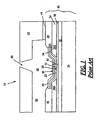
- FIG. 1 is a cross-sectional view, not to scale, of a portion of a prior art micro-fluid ejection head 10.
- the cross-sectional view of FIG.1 shows one of many micro-fluid ejection actuators 12 contained on a micro-fluid ejection head.
- the ejection actuators 12 are formed on a substrate 14.
- the substrate 14 may be made from a wide variety of materials including plastics, ceramics, glass, silicon, semiconductor material, and the like.
- a thermal insulating layer 16 is applied to the substrate between the substrate 14 and the ejection actuators 12.
- the ejection actuators 12 may be formed from an electrically resistive material layer 18, such as TaAl, Ta 2 N, TaAl(O,N), TaAlSi; TaSiC, Ti(N,O), WSi(O,N), TaAlN, and TaAl/Ta.
- the thickness of the resistive material layer 18 may range from about 300 to about 1000 Angstroms.
- the thermal insulation layer 16 may be formed from a thin layer of silicon dioxide and/or doped silicon glass overlying the relatively thick substrate 14.
- the total thickness of the thermal insulation layer 16 may range from about 1 to about 3 microns thick.
- the underlying substrate 14 may have a thickness ranging from about 0.2 to about 0.8 millimeters thick.
- a protective layer 20 overlies the micro-fluid ejection actuators 12.
- the protective layer 20 may be a single material layer or a combination of several material layers.
- the protective layer 20 includes a first passivation layer 22, a second passivation layer 24, and a cavitation layer 26.
- the protective layer 20 is effective to prevent the fluid or other contaminants from adversely affecting the operation and electrical properties of the fluid ejection actuators 12 and provides protection from mechanical abrasion or shock from fluid bubble collapse.
- the first passivation layer 22 may be formed from a dielectric material, such as silicon nitride, or silicon doped diamond-like carbon (Si-DLC) having a thickness ranging from about 1000 to about 3200 Angstroms thick.
- the second passivation layer 24 may also be formed from a dielectric material, such as silicon carbide, silicon nitride, or silicon-doped diamond-like carbon (Si-DLC) having a thickness ranging from about 500 to about 1500 Angstroms thick.
- the combined thickness of the first and second passivation layers 22 and 24 typically ranges from about 1000 to about 5000 Angstroms.
- the cavitation layer 26 is typically formed from tantalum having a thickness greater than about 500 Angstroms thick.
- the cavitation layer 26 may also be made of TaB, Ti, TiW, TiN, WSi, or any other material with a similar thermal capacitance and relatively high hardness.
- the maximum thickness of the cavitation layer 26 is such that the total thickness of protective layer 20 is less than about 7200 Angstroms thick.
- the total thickness of the protective layer 20 is defined as a distance from a top surface 28 of the resistive material layer 18 to an outermost surface 30 of the protective layer 20.
- An ejector stack thickness 32 is defined as the combined thickness of layers 18 and 20.
- the ejection actuator 12 is defined by depositing and etching a metal conductive layer 34 on the resistive layer 18 to provide power and ground conductors 34A and 34B as illustrated in FIG. 1 .
- the conductive layer 34 is typically selected from conductive metals, including but not limited to, gold, aluminum, silver, copper, and the like and has a thickness ranging from about 4,000 to about 15,000 Angstroms.
- insulating layer or dielectric layer 36 typically composed of epoxy photoresist materials, polyimide materials, silicon nitride, silicon carbide, silicon dioxide, spun-on-glass (SOG), laminated polymer and the like.
- the insulating layer 36 and has a thickness ranging from about 5,000 to about 20,000 Angstroms and provides insulation between a second metal layer and conductive layer 34 and corrosion protection of the conductive layer 34.
- Layers 14, 16, 18, 20, 34, and 36 provide a semiconductor substrate 40 for use in the micro-fluid ejection head 10.
- a nozzle plate 42 is adjacent (e.g., attached, as by an adhesive 44 to) the semiconductor substrate 40.
- the nozzle plate 42 contains nozzles 46 corresponding to respective ones of the plurality of ejection actuators 12.
- a fluid in fluid chamber 48 is heated by the ejection actuators 12 to a nucleation temperature of about 325°C. to form a fluid bubble which expels fluid from the fluid chamber 48 through the nozzles 46.
- a fluid supply channel 50 provides fluid to the fluid chamber 48.
- micro-fluid ejection head 10 One disadvantage of the micro-fluid ejection head 10 described above is that the multiplicity of protective layers 20 within the micro-fluid ejection head 10 increases the ejection stack thickness 32, thereby increasing an overall jetting energy required to eject a drop of fluid through the nozzles 46.
- some of the energy ends up as waste heat energy used to heat the protective layer 20 via conduction, while the remainder of the energy is used to heat the fluid adjacent the surface 30 of the cavitation layer 26.
- the surface 30 reaches a fluid superheat limit, a vapor bubble is formed. Once the vapor bubble is formed, the fluid is thermally disconnected from the surface 30. Accordingly, the vapor bubble prevents further thermal energy transfer to the fluid.
- Jetting energy is related to power (power being the product of energy and firing frequency of the micro-fluid ejection actuators 12).
- the temperature rise experienced by the substrate 40 is also related to power.
- Adequate jetting performance and fluid characteristics, such as print quality in the case of an ink ejection device, are related to the temperature rise of the substrate 40.
- the thickness of the protective layer 20 may be minimized in order to reduce power consumption.
- increasing the protective layer 20 thickness to extend the life of the ejection heads may adversely affect the power consumption of the ejection heads as described above.
- a disposable ejection head may provide up to about 10 million ejection cycles before failure of the ejection head.
- longer life ejection heads may require up to 1 billion ejection cycles or more before failure. Accordingly, methods and apparatus for extending the life of the ejection heads without adversely affecting the ejection energy requirements may be provided, such as by the following exemplary embodiments.
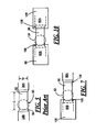
- FIG. 3 is a plan view of a prior art micro-fluid ejection actuator 52 showing a wear pattern 54 adjacent an edge 56 distal from the fluid supply channel 50 ( FIG. 1 ).
- FIG. 4 is a cross-sectional view of a prior art micro-fluid ejection head 58 showing the erosion pattern adjacent the edge 56 of the micro-fluid ejection actuator 52.
- the prior art micro-fluid ejection actuator 52 is an elongate heater resistor have a length L greater than a width W.
- the actuator 52 has a length to width ratio ranging from about 1.5:1 to about 3:1.
- the overall heating area of the actuator 52 may range from about 200 square microns to about 1200 square microns.
- a nozzle 60 can be biased toward the distal edge 56 of the micro-fluid ejection actuator 52, such as in order to reduce air entrapment in the fluid chamber 48 ( FIG. 1 ). However, biasing the nozzle 60 toward the distal edge 56 increases the cavitation and thermal expansion damage adjacent the distal edge 56 of the micro-fluid ejection actuator, as shown in FIGS. 3 and 4 .
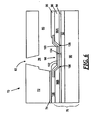
- FIG. 6 is a cross-sectional view, not to scale, of a micro-fluid ejection head 70 according to a first embodiment of the disclosure.
- the ejection head 70 includes a flow feature member 72 attached, as by an adhesive 74, adjacent (e.g., to) a semiconductor substrate 76.
- the flow feature member 72 has a thickness ranging from about 5 to 65 microns, and can be made from a chemically resistant polymer such as polyimide.
- Flow features such as a fluid chamber 78, fluid supply channel 80 and nozzle 82, can be formed in the flow feature member 72 by conventional techniques, such as laser ablation.
- the embodiments described herein are not limited by the foregoing flow feature member 72.
- the flow feature member may comprise fluid chambers and the fluid supply channel in a thick film layer to which a nozzle plate is attached, or the flow features may be formed in both a thick film layer and a nozzle plate.
- FIG. 9 illustrated below, illustrates an embodiment of a micro-fluid ejection head 84 having a thick film layer 86 and nozzle plate 88 attached to the thick film layer 86.
- the semiconductor substrate 76 to which the flow feature member 72 is attached includes a support substrate 90 made of an insulating or semiconductive material as described above with reference to FIG. 1 .
- a semiconductive material for substrate 90 an insulating layer 92 similar to layer 16 is applied to the substrate 90.
- a conductive layer 96 similar to conductive layer 34 is applied to the resistive layer 94 and is etched to provide the power and ground conductors 96A and 96B for activating a micro-fluid ejection actuator 98 defined between the conductors 96A and 96B.
- An advantage of at least some of the disclosed embodiments is that a number and thickness of protective layers for the micro-fluid ejection actuator 98 may be reduced in order to reduce power consumption without adversely affecting the life of the micro-fluid ejection actuators 98.
- the ejection head 70 has a single protective layer 100 and, optionally, a relatively thin cavitation layer 102.
- the protective layer 100 may be provided by a material selected from the group consisting of diamond-like carbon (DLC), silicon doped diamond-like carbon (Si-DLC) titanium, tantalum, silicon nitride and an oxidized metal.
- the thickness of the protective layer 100 may range from about 400 to about 3000 Angstroms.
- Such a protective layer thickness provides an ejection actuator stack 104 having a thickness ranging from about 1200 to about 6500 Angstroms.
- the cavitation layer 102 may have a thickness ranging from about 500 to about 3000 Angstroms.
- a polymeric layer 108 having a degradation temperature of less than about 400° C. is applied to the protective layers 100 and 102 and conductive layer 96 so that the polymeric layer overlaps a portion of the micro-fluid ejection actuator 98 as shown in plan view in FIG. 7 adjacent the distal edge 106 thereof. Due to the relatively low degradation temperature of the polymeric layer 108, the overlapped portion of the actuator 98 should be less than about five microns. Typically, the overlapped portion of the actuator 98 will range from about one to about four microns.
- a temperature profile for the micro-fluid ejection actuator 98 is shown by Curve A in FIG. 8 .
- the micro-fluid ejection actuator 98 has a temperature of about 400° C. in a central portion of the actuator whereas, the edge 106 of the actuator has a temperature of about 150° C.
- the temperature is about 325° C. which is the nucleation temperature indicated by dashed line 110 for ejecting fluid from the micro-fluid ejection head 70. Accordingly, if less than five microns of the actuator 98 adjacent edge 106 is overlapped with the polymeric layer 108, the polymeric layer may be below its decomposition temperature.
- a suitable polymeric layer 108 having a degradation temperature below about 400° C. is a cross-linked epoxy material such as described in U.S. Patent No. 6,830,646 to Patil et al.
- the polymeric layer 108 in the case of micro-fluid ejection head 70, may be applied as a planarisation layer having a thickness averaging from about one to about ten microns.
- Spin coating, spraying, dipping, or roll coating processes may be used to apply the polymeric layer 108 to the conductive layer 96 and protective layers 100 and 102. It will be appreciated that the overlapped portion of the actuator 98 may have a greater thickness of polymeric layer 108 so that a relatively smooth planarization layer may be obtained.
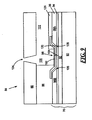
- the micro-fluid ejection head 84 illustrated in FIGS. 9 and 10 includes a thick film layer 86 providing the flow feature member containing a fluid chamber 120 and fluid supply channel 122.
- the thick film layer 86 may also be made of a cross-linked epoxy material as set forth above.
- the thick film layer 86 has a thickness ranging from about 4 to about 40 microns or more.
- the thick film layer overlaps a portion of the micro-fluid ejection actuator 98 as shown in FIGS. 9 and 10 .
- the overlapped portion, adjacent the distal edge 106 may also be less than about five microns and may range from about one to about four microns.
- the thick film layer 86 may be made of the same material as the polymeric layer 108; in which case there may be no need for a separate polymeric layer 108 between the thick film layer 86 and the conductive layer 96 and protective layers 100 and 102.
- the thick film layer 86 may be applied in the same manner as the polymeric layer 108 described above.
- Each of the polymeric layer 108 and thick film layer 86 may be photoimaged and developed using conventional photoimaging and developing techniques to provide the less than five micron overlap of the actuator 98. In the case of the thick film layer 86, the photoimaging and developing techniques may also be used to provide the fluid chamber 120 and fluid supply channel 122 therein.
- a nozzle plate 88 made of a polyimide material or a photoresist material may be attached to the thick film layer 86.
- a nozzle 124 for each of the actuators may be laser ablated in the nozzle plate 88. If the nozzle plate 88 is made of a photoresist material, photoimaging and developing techniques may be used to make the nozzle 124.
- a polymeric layer 126 may overlap a proximal edge 128 of the actuator 98 so that both the distal edge 106 and the proximal edge 128 of the actuator 98 are overlapped less than about five microns, typically from about one to about four microns.
- the polymeric layer 126 as illustrated in FIGS. 9 and 10 , may likewise be applied to overlap the proximal edge 128 of the actuator illustrated in FIGS. 6 and 7 .
- the polymeric layer 126 may be the same as the thick film layer 86 except that the thickness of the polymeric layer 126 will be reduced in the fluid supply channel 122 of the ejection head 84 by imaging and developing the polymeric layer 126.
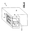
- the micro-fluid ejection head 70 or 84 may be permanently or removably attached to a fluid supply cartridge 128 as shown in FIG. 11 . As shown in FIG. 5 , the ejection head 70 or 84 may be attached to an ejection head portion 130 of the fluid cartridge 128.
- a main body 132 of the cartridge 128 includes a fluid reservoir for supply of fluid to the micro-fluid ejection head 70 or 84.
- micro-fluid ejection actuator 98 to provide activation of micro-fluid ejection actuator 98 on demand from the control device to which the fluid cartridge 128 is attached.
- the disclosure is not limited to the fluid cartridges 128 as illustrated in FIG. 11 as the micro-fluid ejection head 70 or 84 according to the disclosure may be used for a wide variety of fluid cartridges, wherein the ejection head 70 or 84 may be remote from the fluid reservoir of main body 128.
Landscapes
- Physics & Mathematics (AREA)
- Geometry (AREA)
- Particle Formation And Scattering Control In Inkjet Printers (AREA)
- Nozzles (AREA)
- Micromachines (AREA)
Claims (20)
- Mikrofluidausstoßkopf (70), mit
einem Substrat (76) mit einer Mehrzahl thermischer Ausstoßaktuatoren (98), die darauf angeordnet sind, wobei jeder der thermischen Ausstoßaktuatoren eine Widerstandschicht und eine Schutzsicht zum Schützen einer Oberfläche der Widerstandsschicht aufweist, wobei die Widerstandsschicht und die Schutzschicht zusammen eine Aktuatorstapeldicke definieren, und wobei das Substrat einen Abschnitt frei von leitfähigem Material aufweist, wobei die thermischen Ausstoßaktuatoren auf dem Abschnitt vorgesehen sind, der frei von leitfähigem Material ist;
einem benachbart zu dem Substrat angeordneten Durchflussfunktionselement (72), das einen Fluidzuführkanal definiert, sowie eine Fluidkammer, die zumindest einem der thermischen Ausstoßaktuatoren zugeordnet ist und in Fluidverbindung mit dem Fluidzuführkanal steht, und eine Düse, die über dem zumindest einem thermischen Ausststossaktuator gebildet ist, wobei die Düse versetzt zu einer Seite der Fluidkammer entgegengesetzt zu dem Fluidzuführkanal angeordnet ist; und einer Polymerschicht (108) mit einer Zersetzungstemperatur von weniger als 400°C, die einen Abschnitt des zumindest einen thermischen Ausstoßaktuators (98) überlappt, der der Fluidkammer zugeordnet ist und weniger als fünf Mikrometer entfernt von zumindest einer Kante des zumindest einen thermischen Ausstoßaktuators gegenüber dem Fluidzuführkanal angeordnet ist, und wobei die Polymerschicht die Widerstandsschicht und die Schutzschicht in dem Abschnitt überlappt, der frei von leitfähigem Material ist. - Mikrofluidausstoßkopf (70) nach Anspruch 1, wobei die Aktuatorstapeldicke in einem Bereich von 1200 bis 1600 Angström (120 bis 650 nm) liegt und eine Ausstoßenergie pro Volumeneinheit von zwei bis vier Gigajoule pro Kubikzentimeter bereitstellt.
- Mikrofluidausstoßkopf (70) nach Anspruch 1, wobei die Widerstandsschicht eine Dicke aufweist, die in einem Bereich von 300 bis 1000 Angström (30 bis 100 nm) liegt.
- Mikrofluidausstoßkopf (70) nach Anspruch 1, wobei jeder der thermischen Ausstoßaktuatoren (98) einen Fluidheizabschnitt mit einer Flächengröße aufweist, die im Bereich von 200 Quadratmikrometer bis 1200 Quadratmikrometer liegt.
- Mikrofluidausstoßkopf (70) nach Anspruch 1, wobei die Schutzschicht eine Dicke aufweist, die im Bereich von 900 bis 5500 Angström (90 bis 550 nm) liegt.
- Mikrofluidausstoßkopf (70) nach Anspruch 1, wobei die Widerstandsschicht eine Tantal-Aluminium-Legierung und die Schutzschicht ein Material aufweist, das aus der Gruppe enthaltend amorphen Kohlenstoff (DLC), siliziumdotierten amorphen Kohlenstoff, Siliziumnitird, Titan, Tantal und einer oxidierten Metallschicht ausgewählt wurde.
- Mikrofluidausstoßkopf (70) nach Anspruch 6, wobei die Widerstandsschicht ein Material aufweist, das aus der Gruppe enthaltend Tantal-Aluminium (TaAl), Tantal-Nitrid (TaN), Tantal-Aluminium-Nitrid (TaAl:N) und zusammengesetzte Schichten mit Tantal und Tantal-Aluminium (Ta + TaAl) ausgewählt wurde.
- Mikrofluidausstoßkopf (70) nach Anspruch 1, wobei die Polymerschicht (108) ein vernetztes Epoxidmaterial aufweist.
- Mikrofluidausstoßkopf (70) nach Anspruch 1, wobei die Polymerschicht (108) eine Kante des zumindest einen Aktuators in einem Ausmass überlappt, der im Bereich von einem bis vier Mikrometer liegt.
- Mikrofluidausstoßkopf (70) nach Anspruch 1, wobei die Polymerschicht (108) den wenigstens einen Ausstoßaktuator entgegensetzt zu Kantenabschnitten hiervon in einem Ausmass überlappt, das im Bereich von einem bis vier Mikrometer liegt.
- Mikrofluidausstoßkopf (70) nach Anspruch 1, wobei die Aktuatoren (98) längliche Aktuatoren mit einem Länge-zu-Breite-Verhältnis sind, das im Bereich von 1,5:5 bis 5:1 liegt.
- Verfahren zum Herstellen eines Mikrofluidausstoßkopfes (70) mit einem Substrat (76) mit einer Mehrzahl thermischer Ausstoßaktuatoren (98), wobei jeder der thermischen Ausstoßaktuatoren eine Widerstandschicht und eine Schutzsicht zum Schützen einer Oberfläche der Widerstandsschicht aufweist, wobei das Substrat einen Abschnitt frei von leitfähigem Material aufweist, und ein Durchflussfunktionselement (72) aufweist, das einen Fluidzuführkanal, eine Fluidkammer, die zumindest einem der thermischen Ausstoßaktuatoren zugeordnet ist und in Fluidverbindung mit dem Fluidzuführkanal steht, und eine Düse, die über dem zumindest einem thermischen Ausstoßaktuator gebildet ist, definiert, wobei die Düse versetzt zu einer Seite der Fluidkammer distal bzw. fern von dem Fluidzuführkanal angeordnet ist, wobei das Verfahren aufweist:Abscheiden einer Polymerschicht (108) mit einer Zersetzungstemperatur von weniger als 400°C in überlappender Beziehung mit zumindest einem Abschnitt des zumindest einen thermischen Aktuators, wobei die Polymerschicht weniger als fünf Mikrometer den zumindest einem Aktuator benachbart an einer Kante hiervon distal von dem Fluidzuführkanal überlappt, und wobei die Polymerschicht die Widerstandsschicht und die Schutzschicht in dem Abschnitt überlappt, der frei von leitfähigem Material ist.
- Verfahren nach Anspruch 12, wobei das Durchflussfunktionselement eine Polymerdickfilmschicht aufweist.
- Verfahren nach Anspruch 13, wobei der Schritt des Abscheidens einer Polymerschicht die Polymerdickfilmschicht bereitstellt.
- Verfahren nach Anspruch 12, wobei das Durchflussfunktionselement (76) ein einheitliches bzw. einstückiges und/oder materialeinheitliches Polyimidelement mit Fluidzuführkanälen, Fluidkammer und Düsen aufweist.
- Verfahren nach Anspruch 15, wobei die Polymerschicht (108) eine Planarisierungsschicht mit einer Dicke aufweist, die im Bereich vom einem bis sechs Mikrometer liegt.
- Verfahren nach Anspruch 16, wobei die Planarisierungsschicht ein vernetztes Epoxidmaterial aufweist.
- Verfahren nach Anspruch 12, wobei die Polymerschicht (108) derart abgeschieden wird, dass die Polymerschicht zumindest einen Aktuator überlappt, wobei das Ausmaß in einem Bereich von einem bis vier Mikrometer liegt.
- Verfahren nach Anspruch 18, wobei die Polymerschicht (108) derart auf dem zumindest einen Aktuator abgeschieden wird, so dass sich überlappende Anschnitte um einen bis vier Mikrometer von den entgegengesetzten Kantenabschnitten hiervon erstrecken.
- Mikrofluidausstoßkopf (70), gefertigt nach dem Verfahren nach Anspruch 12.
Applications Claiming Priority (2)
| Application Number | Priority Date | Filing Date | Title |
|---|---|---|---|
| US11/317,575 US7413289B2 (en) | 2005-12-23 | 2005-12-23 | Low energy, long life micro-fluid ejection device |
| PCT/US2006/049063 WO2007076029A2 (en) | 2005-12-23 | 2006-12-21 | Low energy, long life micro-fluid ejection device |
Publications (3)
| Publication Number | Publication Date |
|---|---|
| EP1968797A2 EP1968797A2 (de) | 2008-09-17 |
| EP1968797A4 EP1968797A4 (de) | 2010-08-11 |
| EP1968797B1 true EP1968797B1 (de) | 2015-03-04 |
Family
ID=38193097
Family Applications (1)
| Application Number | Title | Priority Date | Filing Date |
|---|---|---|---|
| EP06848047.4A Not-in-force EP1968797B1 (de) | 2005-12-23 | 2006-12-21 | Energiearme, langlebige mikrofluidausstossvorrichtung |
Country Status (8)
| Country | Link |
|---|---|
| US (2) | US7413289B2 (de) |
| EP (1) | EP1968797B1 (de) |
| CN (1) | CN101346235B (de) |
| AU (1) | AU2006330919B2 (de) |
| BR (1) | BRPI0620293A2 (de) |
| CA (1) | CA2631454C (de) |
| TW (1) | TWI330597B (de) |
| WO (1) | WO2007076029A2 (de) |
Families Citing this family (15)
| Publication number | Priority date | Publication date | Assignee | Title |
|---|---|---|---|---|
| KR100643328B1 (ko) * | 2005-06-21 | 2006-11-10 | 삼성전자주식회사 | 잉크젯 프린터 헤드 및 그 제조방법 |
| US7413289B2 (en) * | 2005-12-23 | 2008-08-19 | Lexmark International, Inc. | Low energy, long life micro-fluid ejection device |
| US8409458B2 (en) * | 2007-03-02 | 2013-04-02 | Texas Instruments Incorporated | Process for reactive ion etching a layer of diamond like carbon |
| CN101873935A (zh) * | 2007-11-24 | 2010-10-27 | 惠普开发有限公司 | 具有加热电阻边缘保护层的喷墨打印装置打印头芯片 |
| TWI394239B (zh) * | 2008-12-17 | 2013-04-21 | Univ Ishou | The integrated circuit with the isolation layer of metal ion migration and its encapsulation structure |
| US9138994B2 (en) | 2009-03-03 | 2015-09-22 | Taiwan Semiconductor Manufacturing Company, Ltd. | MEMS devices and methods of fabrication thereof |
| US8281482B2 (en) * | 2009-08-25 | 2012-10-09 | Zamtec Limited | Method of fabricating crack-resistant thermal bend actuator |
| US8079668B2 (en) | 2009-08-25 | 2011-12-20 | Silverbrook Research Pty Ltd | Crack-resistant thermal bend actuator |
| WO2011022750A1 (en) * | 2009-08-25 | 2011-03-03 | Silverbrook Research Pty Ltd | Crack-resistant thermal bend actuator |
| US8784511B2 (en) * | 2009-09-28 | 2014-07-22 | Stmicroelectronics (Tours) Sas | Method for forming a thin-film lithium-ion battery |
| EP2563596B1 (de) * | 2010-04-29 | 2015-07-22 | Hewlett Packard Development Company, L.P. | Flüssigkeitsausstossvorrichtung |
| WO2015005933A1 (en) * | 2013-07-12 | 2015-01-15 | Hewlett-Packard Development Company, L.P. | Thermal inkjet printhead stack with amorphous thin metal protective layer |
| US10177310B2 (en) | 2014-07-30 | 2019-01-08 | Hewlett Packard Enterprise Development Lp | Amorphous metal alloy electrodes in non-volatile device applications |
| TWI671211B (zh) * | 2014-11-19 | 2019-09-11 | 愛爾蘭商滿捷特科技公司 | 生存期獲得改善之噴墨噴嘴裝置 |
| US10532571B2 (en) | 2015-03-12 | 2020-01-14 | Hewlett-Packard Development Company, L.P. | Printhead structure |
Family Cites Families (11)
| Publication number | Priority date | Publication date | Assignee | Title |
|---|---|---|---|---|
| JPH0613219B2 (ja) * | 1983-04-30 | 1994-02-23 | キヤノン株式会社 | インクジェットヘッド |
| JPS60116451A (ja) * | 1983-11-30 | 1985-06-22 | Canon Inc | 液体噴射記録ヘツド |
| US4794411A (en) * | 1987-10-19 | 1988-12-27 | Hewlett-Packard Company | Thermal ink-jet head structure with orifice offset from resistor |
| US5831648A (en) | 1992-05-29 | 1998-11-03 | Hitachi Koki Co., Ltd. | Ink jet recording head |
| DE69621665T2 (de) * | 1995-03-03 | 2003-03-06 | Canon K.K., Tokio/Tokyo | Tintenstrahlkopf, Substrat für einen Tintenstrahlkopf und Tintenstrahlgerät |
| JPH09300623A (ja) | 1996-05-17 | 1997-11-25 | Hitachi Koki Co Ltd | インクジェット記録ヘッド及びその装置 |
| US6908563B2 (en) * | 2001-11-27 | 2005-06-21 | Canon Kabushiki Kaisha | Ink-jet head, and method for manufacturing the same |
| JP2004230811A (ja) * | 2003-01-31 | 2004-08-19 | Fuji Photo Film Co Ltd | 液滴吐出ヘッド |
| US6902256B2 (en) | 2003-07-16 | 2005-06-07 | Lexmark International, Inc. | Ink jet printheads |
| JP4350658B2 (ja) | 2004-03-24 | 2009-10-21 | キヤノン株式会社 | 液体吐出ヘッド用基板及び液体吐出ヘッド |
| US7413289B2 (en) | 2005-12-23 | 2008-08-19 | Lexmark International, Inc. | Low energy, long life micro-fluid ejection device |
-
2005
- 2005-12-23 US US11/317,575 patent/US7413289B2/en active Active
-
2006
- 2006-12-21 BR BRPI0620293-4A patent/BRPI0620293A2/pt not_active IP Right Cessation
- 2006-12-21 CN CN2006800487656A patent/CN101346235B/zh not_active Expired - Fee Related
- 2006-12-21 CA CA2631454A patent/CA2631454C/en not_active Expired - Fee Related
- 2006-12-21 WO PCT/US2006/049063 patent/WO2007076029A2/en not_active Ceased
- 2006-12-21 AU AU2006330919A patent/AU2006330919B2/en not_active Ceased
- 2006-12-21 EP EP06848047.4A patent/EP1968797B1/de not_active Not-in-force
- 2006-12-22 TW TW095148622A patent/TWI330597B/zh not_active IP Right Cessation
-
2008
- 2008-06-25 US US12/145,606 patent/US7784918B2/en not_active Expired - Lifetime
Also Published As
| Publication number | Publication date |
|---|---|
| TW200732163A (en) | 2007-09-01 |
| AU2006330919A1 (en) | 2007-07-05 |
| EP1968797A2 (de) | 2008-09-17 |
| WO2007076029A2 (en) | 2007-07-05 |
| CN101346235B (zh) | 2011-04-13 |
| EP1968797A4 (de) | 2010-08-11 |
| CA2631454A1 (en) | 2007-07-05 |
| WO2007076029A3 (en) | 2008-04-17 |
| AU2006330919B2 (en) | 2010-10-28 |
| CN101346235A (zh) | 2009-01-14 |
| BRPI0620293A2 (pt) | 2011-11-08 |
| US20080259131A1 (en) | 2008-10-23 |
| CA2631454C (en) | 2010-03-30 |
| TWI330597B (en) | 2010-09-21 |
| US7784918B2 (en) | 2010-08-31 |
| US7413289B2 (en) | 2008-08-19 |
| US20070146436A1 (en) | 2007-06-28 |
Similar Documents
| Publication | Publication Date | Title |
|---|---|---|
| US7784918B2 (en) | Low energy, long life micro-fluid ejection device | |
| US8366952B2 (en) | Low ejection energy micro-fluid ejection heads | |
| JPH03202353A (ja) | サーマルインクジェット印字ヘッド | |
| KR20100027761A (ko) | 잉크 토출 장치 및 그 제조방법 | |
| US20100321447A1 (en) | Protective layers for micro-fluid ejection devices and methods for depositing same | |
| KR101235808B1 (ko) | 잉크젯 프린트헤드 및 그 제조방법 | |
| KR100433528B1 (ko) | 잉크젯 프린트헤드 및 그 제조방법 | |
| US7024768B2 (en) | Fluid ejection device having a layer with a discontinuity | |
| KR20100011652A (ko) | 잉크젯 프린트헤드 및 그 제조방법 | |
| US7178904B2 (en) | Ultra-low energy micro-fluid ejection device | |
| KR20100021166A (ko) | 열구동 방식 잉크젯 프린트헤드 및 그 구동방법 | |
| KR100553912B1 (ko) | 잉크젯 프린트헤드 및 그 제조방법 | |
| KR100717034B1 (ko) | 열구동 방식의 잉크젯 프린트헤드 | |
| KR20080018506A (ko) | 잉크젯 프린트헤드 및 그 제조방법 | |
| MX2008008236A (en) | Low energy, long life micro-fluid ejection device | |
| KR100818282B1 (ko) | 잉크젯 프린트헤드 | |
| KR100723414B1 (ko) | 열구동 방식의 잉크젯 프린트헤드 | |
| JP2004203049A (ja) | インクジェットプリントヘッド及びその製造方法 | |
| KR100619077B1 (ko) | TiN0.3로 이루어진 열발생저항체를 구비하는잉크젯프린트헤드 | |
| WO2009005489A1 (en) | Protective layers for micro-fluid ejection devices | |
| KR20060069564A (ko) | 잉크젯 프린트 헤드 |
Legal Events
| Date | Code | Title | Description |
|---|---|---|---|
| PUAI | Public reference made under article 153(3) epc to a published international application that has entered the european phase |
Free format text: ORIGINAL CODE: 0009012 |
|
| 17P | Request for examination filed |
Effective date: 20080708 |
|
| AK | Designated contracting states |
Kind code of ref document: A2 Designated state(s): AT BE BG CH CY CZ DE DK EE ES FI FR GB GR HU IE IS IT LI LT LU LV MC NL PL PT RO SE SI SK TR |
|
| AX | Request for extension of the european patent |
Extension state: AL BA HR MK RS |
|
| DAX | Request for extension of the european patent (deleted) | ||
| RBV | Designated contracting states (corrected) |
Designated state(s): DE FR GB |
|
| A4 | Supplementary search report drawn up and despatched |
Effective date: 20100713 |
|
| RAP1 | Party data changed (applicant data changed or rights of an application transferred) |
Owner name: LEXMARK INTERNATIONAL, INC. |
|
| 17Q | First examination report despatched |
Effective date: 20110620 |
|
| RAP1 | Party data changed (applicant data changed or rights of an application transferred) |
Owner name: FUNAI ELECTRIC CO., LTD. |
|
| GRAP | Despatch of communication of intention to grant a patent |
Free format text: ORIGINAL CODE: EPIDOSNIGR1 |
|
| INTG | Intention to grant announced |
Effective date: 20140917 |
|
| GRAS | Grant fee paid |
Free format text: ORIGINAL CODE: EPIDOSNIGR3 |
|
| GRAA | (expected) grant |
Free format text: ORIGINAL CODE: 0009210 |
|
| AK | Designated contracting states |
Kind code of ref document: B1 Designated state(s): DE FR GB |
|
| REG | Reference to a national code |
Ref country code: GB Ref legal event code: FG4D |
|
| REG | Reference to a national code |
Ref country code: DE Ref legal event code: R096 Ref document number: 602006044731 Country of ref document: DE Effective date: 20150416 |
|
| REG | Reference to a national code |
Ref country code: FR Ref legal event code: PLFP Year of fee payment: 10 |
|
| REG | Reference to a national code |
Ref country code: DE Ref legal event code: R097 Ref document number: 602006044731 Country of ref document: DE |
|
| PLBE | No opposition filed within time limit |
Free format text: ORIGINAL CODE: 0009261 |
|
| STAA | Information on the status of an ep patent application or granted ep patent |
Free format text: STATUS: NO OPPOSITION FILED WITHIN TIME LIMIT |
|
| PGFP | Annual fee paid to national office [announced via postgrant information from national office to epo] |
Ref country code: GB Payment date: 20151216 Year of fee payment: 10 |
|
| 26N | No opposition filed |
Effective date: 20151207 |
|
| PGFP | Annual fee paid to national office [announced via postgrant information from national office to epo] |
Ref country code: FR Payment date: 20151110 Year of fee payment: 10 |
|
| REG | Reference to a national code |
Ref country code: DE Ref legal event code: R084 Ref document number: 602006044731 Country of ref document: DE |
|
| GBPC | Gb: european patent ceased through non-payment of renewal fee |
Effective date: 20161221 |
|
| REG | Reference to a national code |
Ref country code: FR Ref legal event code: ST Effective date: 20170831 |
|
| PG25 | Lapsed in a contracting state [announced via postgrant information from national office to epo] |
Ref country code: FR Free format text: LAPSE BECAUSE OF NON-PAYMENT OF DUE FEES Effective date: 20170102 |
|
| PG25 | Lapsed in a contracting state [announced via postgrant information from national office to epo] |
Ref country code: GB Free format text: LAPSE BECAUSE OF NON-PAYMENT OF DUE FEES Effective date: 20161221 |
|
| PGFP | Annual fee paid to national office [announced via postgrant information from national office to epo] |
Ref country code: DE Payment date: 20191210 Year of fee payment: 14 |
|
| REG | Reference to a national code |
Ref country code: DE Ref legal event code: R082 Ref document number: 602006044731 Country of ref document: DE |
|
| REG | Reference to a national code |
Ref country code: DE Ref legal event code: R119 Ref document number: 602006044731 Country of ref document: DE |
|
| PG25 | Lapsed in a contracting state [announced via postgrant information from national office to epo] |
Ref country code: DE Free format text: LAPSE BECAUSE OF NON-PAYMENT OF DUE FEES Effective date: 20210701 |