EP1968039A1 - Organic light emitting display - Google Patents
Organic light emitting display Download PDFInfo
- Publication number
- EP1968039A1 EP1968039A1 EP08250708A EP08250708A EP1968039A1 EP 1968039 A1 EP1968039 A1 EP 1968039A1 EP 08250708 A EP08250708 A EP 08250708A EP 08250708 A EP08250708 A EP 08250708A EP 1968039 A1 EP1968039 A1 EP 1968039A1
- Authority
- EP
- European Patent Office
- Prior art keywords
- switch
- electrically coupled
- light emitting
- organic light
- capacitor
- Prior art date
- Legal status (The legal status is an assumption and is not a legal conclusion. Google has not performed a legal analysis and makes no representation as to the accuracy of the status listed.)
- Ceased
Links
Images

Classifications
-
- G—PHYSICS
- G09—EDUCATION; CRYPTOGRAPHY; DISPLAY; ADVERTISING; SEALS
- G09G—ARRANGEMENTS OR CIRCUITS FOR CONTROL OF INDICATING DEVICES USING STATIC MEANS TO PRESENT VARIABLE INFORMATION
- G09G3/00—Control arrangements or circuits, of interest only in connection with visual indicators other than cathode-ray tubes
- G09G3/20—Control arrangements or circuits, of interest only in connection with visual indicators other than cathode-ray tubes for presentation of an assembly of a number of characters, e.g. a page, by composing the assembly by combination of individual elements arranged in a matrix no fixed position being assigned to or needed to be assigned to the individual characters or partial characters
- G09G3/22—Control arrangements or circuits, of interest only in connection with visual indicators other than cathode-ray tubes for presentation of an assembly of a number of characters, e.g. a page, by composing the assembly by combination of individual elements arranged in a matrix no fixed position being assigned to or needed to be assigned to the individual characters or partial characters using controlled light sources
- G09G3/30—Control arrangements or circuits, of interest only in connection with visual indicators other than cathode-ray tubes for presentation of an assembly of a number of characters, e.g. a page, by composing the assembly by combination of individual elements arranged in a matrix no fixed position being assigned to or needed to be assigned to the individual characters or partial characters using controlled light sources using electroluminescent panels
-
- G—PHYSICS
- G09—EDUCATION; CRYPTOGRAPHY; DISPLAY; ADVERTISING; SEALS
- G09G—ARRANGEMENTS OR CIRCUITS FOR CONTROL OF INDICATING DEVICES USING STATIC MEANS TO PRESENT VARIABLE INFORMATION
- G09G3/00—Control arrangements or circuits, of interest only in connection with visual indicators other than cathode-ray tubes
- G09G3/20—Control arrangements or circuits, of interest only in connection with visual indicators other than cathode-ray tubes for presentation of an assembly of a number of characters, e.g. a page, by composing the assembly by combination of individual elements arranged in a matrix no fixed position being assigned to or needed to be assigned to the individual characters or partial characters
- G09G3/22—Control arrangements or circuits, of interest only in connection with visual indicators other than cathode-ray tubes for presentation of an assembly of a number of characters, e.g. a page, by composing the assembly by combination of individual elements arranged in a matrix no fixed position being assigned to or needed to be assigned to the individual characters or partial characters using controlled light sources
- G09G3/30—Control arrangements or circuits, of interest only in connection with visual indicators other than cathode-ray tubes for presentation of an assembly of a number of characters, e.g. a page, by composing the assembly by combination of individual elements arranged in a matrix no fixed position being assigned to or needed to be assigned to the individual characters or partial characters using controlled light sources using electroluminescent panels
- G09G3/32—Control arrangements or circuits, of interest only in connection with visual indicators other than cathode-ray tubes for presentation of an assembly of a number of characters, e.g. a page, by composing the assembly by combination of individual elements arranged in a matrix no fixed position being assigned to or needed to be assigned to the individual characters or partial characters using controlled light sources using electroluminescent panels semiconductive, e.g. using light-emitting diodes [LED]
- G09G3/3208—Control arrangements or circuits, of interest only in connection with visual indicators other than cathode-ray tubes for presentation of an assembly of a number of characters, e.g. a page, by composing the assembly by combination of individual elements arranged in a matrix no fixed position being assigned to or needed to be assigned to the individual characters or partial characters using controlled light sources using electroluminescent panels semiconductive, e.g. using light-emitting diodes [LED] organic, e.g. using organic light-emitting diodes [OLED]
- G09G3/3225—Control arrangements or circuits, of interest only in connection with visual indicators other than cathode-ray tubes for presentation of an assembly of a number of characters, e.g. a page, by composing the assembly by combination of individual elements arranged in a matrix no fixed position being assigned to or needed to be assigned to the individual characters or partial characters using controlled light sources using electroluminescent panels semiconductive, e.g. using light-emitting diodes [LED] organic, e.g. using organic light-emitting diodes [OLED] using an active matrix
- G09G3/3233—Control arrangements or circuits, of interest only in connection with visual indicators other than cathode-ray tubes for presentation of an assembly of a number of characters, e.g. a page, by composing the assembly by combination of individual elements arranged in a matrix no fixed position being assigned to or needed to be assigned to the individual characters or partial characters using controlled light sources using electroluminescent panels semiconductive, e.g. using light-emitting diodes [LED] organic, e.g. using organic light-emitting diodes [OLED] using an active matrix with pixel circuitry controlling the current through the light-emitting element
-
- G—PHYSICS
- G09—EDUCATION; CRYPTOGRAPHY; DISPLAY; ADVERTISING; SEALS
- G09G—ARRANGEMENTS OR CIRCUITS FOR CONTROL OF INDICATING DEVICES USING STATIC MEANS TO PRESENT VARIABLE INFORMATION
- G09G3/00—Control arrangements or circuits, of interest only in connection with visual indicators other than cathode-ray tubes
- G09G3/20—Control arrangements or circuits, of interest only in connection with visual indicators other than cathode-ray tubes for presentation of an assembly of a number of characters, e.g. a page, by composing the assembly by combination of individual elements arranged in a matrix no fixed position being assigned to or needed to be assigned to the individual characters or partial characters
-
- G—PHYSICS
- G09—EDUCATION; CRYPTOGRAPHY; DISPLAY; ADVERTISING; SEALS
- G09G—ARRANGEMENTS OR CIRCUITS FOR CONTROL OF INDICATING DEVICES USING STATIC MEANS TO PRESENT VARIABLE INFORMATION
- G09G3/00—Control arrangements or circuits, of interest only in connection with visual indicators other than cathode-ray tubes
- G09G3/20—Control arrangements or circuits, of interest only in connection with visual indicators other than cathode-ray tubes for presentation of an assembly of a number of characters, e.g. a page, by composing the assembly by combination of individual elements arranged in a matrix no fixed position being assigned to or needed to be assigned to the individual characters or partial characters
- G09G3/22—Control arrangements or circuits, of interest only in connection with visual indicators other than cathode-ray tubes for presentation of an assembly of a number of characters, e.g. a page, by composing the assembly by combination of individual elements arranged in a matrix no fixed position being assigned to or needed to be assigned to the individual characters or partial characters using controlled light sources
- G09G3/30—Control arrangements or circuits, of interest only in connection with visual indicators other than cathode-ray tubes for presentation of an assembly of a number of characters, e.g. a page, by composing the assembly by combination of individual elements arranged in a matrix no fixed position being assigned to or needed to be assigned to the individual characters or partial characters using controlled light sources using electroluminescent panels
- G09G3/32—Control arrangements or circuits, of interest only in connection with visual indicators other than cathode-ray tubes for presentation of an assembly of a number of characters, e.g. a page, by composing the assembly by combination of individual elements arranged in a matrix no fixed position being assigned to or needed to be assigned to the individual characters or partial characters using controlled light sources using electroluminescent panels semiconductive, e.g. using light-emitting diodes [LED]
-
- H—ELECTRICITY
- H05—ELECTRIC TECHNIQUES NOT OTHERWISE PROVIDED FOR
- H05B—ELECTRIC HEATING; ELECTRIC LIGHT SOURCES NOT OTHERWISE PROVIDED FOR; CIRCUIT ARRANGEMENTS FOR ELECTRIC LIGHT SOURCES, IN GENERAL
- H05B33/00—Electroluminescent light sources
- H05B33/12—Light sources with substantially two-dimensional [2D] radiating surfaces
-
- G—PHYSICS
- G09—EDUCATION; CRYPTOGRAPHY; DISPLAY; ADVERTISING; SEALS
- G09G—ARRANGEMENTS OR CIRCUITS FOR CONTROL OF INDICATING DEVICES USING STATIC MEANS TO PRESENT VARIABLE INFORMATION
- G09G2300/00—Aspects of the constitution of display devices
- G09G2300/08—Active matrix structure, i.e. with use of active elements, inclusive of non-linear two terminal elements, in the pixels together with light emitting or modulating elements
- G09G2300/0809—Several active elements per pixel in active matrix panels
- G09G2300/0819—Several active elements per pixel in active matrix panels used for counteracting undesired variations, e.g. feedback or autozeroing
-
- G—PHYSICS
- G09—EDUCATION; CRYPTOGRAPHY; DISPLAY; ADVERTISING; SEALS
- G09G—ARRANGEMENTS OR CIRCUITS FOR CONTROL OF INDICATING DEVICES USING STATIC MEANS TO PRESENT VARIABLE INFORMATION
- G09G2300/00—Aspects of the constitution of display devices
- G09G2300/08—Active matrix structure, i.e. with use of active elements, inclusive of non-linear two terminal elements, in the pixels together with light emitting or modulating elements
- G09G2300/0809—Several active elements per pixel in active matrix panels
- G09G2300/0842—Several active elements per pixel in active matrix panels forming a memory circuit, e.g. a dynamic memory with one capacitor
- G09G2300/0852—Several active elements per pixel in active matrix panels forming a memory circuit, e.g. a dynamic memory with one capacitor being a dynamic memory with more than one capacitor
-
- G—PHYSICS
- G09—EDUCATION; CRYPTOGRAPHY; DISPLAY; ADVERTISING; SEALS
- G09G—ARRANGEMENTS OR CIRCUITS FOR CONTROL OF INDICATING DEVICES USING STATIC MEANS TO PRESENT VARIABLE INFORMATION
- G09G2300/00—Aspects of the constitution of display devices
- G09G2300/08—Active matrix structure, i.e. with use of active elements, inclusive of non-linear two terminal elements, in the pixels together with light emitting or modulating elements
- G09G2300/0809—Several active elements per pixel in active matrix panels
- G09G2300/0842—Several active elements per pixel in active matrix panels forming a memory circuit, e.g. a dynamic memory with one capacitor
- G09G2300/0861—Several active elements per pixel in active matrix panels forming a memory circuit, e.g. a dynamic memory with one capacitor with additional control of the display period without amending the charge stored in a pixel memory, e.g. by means of additional select electrodes
-
- G—PHYSICS
- G09—EDUCATION; CRYPTOGRAPHY; DISPLAY; ADVERTISING; SEALS
- G09G—ARRANGEMENTS OR CIRCUITS FOR CONTROL OF INDICATING DEVICES USING STATIC MEANS TO PRESENT VARIABLE INFORMATION
- G09G2320/00—Control of display operating conditions
- G09G2320/04—Maintaining the quality of display appearance
- G09G2320/043—Preventing or counteracting the effects of ageing
-
- G—PHYSICS
- G09—EDUCATION; CRYPTOGRAPHY; DISPLAY; ADVERTISING; SEALS
- G09G—ARRANGEMENTS OR CIRCUITS FOR CONTROL OF INDICATING DEVICES USING STATIC MEANS TO PRESENT VARIABLE INFORMATION
- G09G2320/00—Control of display operating conditions
- G09G2320/04—Maintaining the quality of display appearance
- G09G2320/043—Preventing or counteracting the effects of ageing
- G09G2320/045—Compensation of drifts in the characteristics of light emitting or modulating elements
Definitions
- the present invention relates to an organic light emitting display. More particularly, the invention relates to an organic light emitting display that can suppress image sticking due to a decrease in efficiency of an organic light emitting diode and can compensate for a threshold voltage of a drive transistor.
- an organic light emitting display is a display that emits light by electrically exciting a fluorescent or phosphorescent compound.
- the organic light emitting display may display an image by driving N ⁇ M organic light emitting diodes (OLEDs).
- OLEDs organic light emitting diodes
- Each OLED may include an anode electrode (indium tin oxide (ITO)), an organic thin-film layer, and a cathode electrode (metal).
- ITO indium tin oxide
- the organic thin-film layer may have a multi-layer structure including an emitting layer (EML), an electron transport layer (ETL) and a hole transport layer (HTL).
- EML emitting layer
- ETL electron transport layer
- HTL hole transport layer
- the organic thin-film may include a separate electron injecting layer (EIL) and a hole injecting layer (HIL).
- the anode electrode is coupled to a first power supply to supply holes to the EML, and the cathode electrode is coupled with a second power supply to supply electrons to the EML.
- the second power supply has a lower voltage than the first power supply.
- the anode electrode has a positive (+) electric potential and, relative to the anode electrode, the cathode has a (-) electrode potential.
- the HTL accelerates hole(s) supplied from the anode electrode and supplies the hole(s) to the EML.
- the ETL accelerates electron(s) supplied from the cathode electrode and supplies the electron(s) to the EML.
- the electron(s) supplied from the ETL and the hole(s) supplied from the HTL may recombine with each other, thereby generating a predetermined amount of light.
- the EML may include organic material that may generate one of red light (R), green light (G) and blue light (B) when the electron(s) and hole(s) recombine therein.
- the invention sets out to provide an organic light emitting display that substantially overcomes one or more of the problems due to the limitations and disadvantages of the related art.
- an organic light emitting display including a driving transistor electrically coupled to a first power line, a first switch electrically coupled to the driving transistor and an emission line, a second switch electrically coupled to the driving transistor and a previous scan line, a third switch electrically coupled to the first switch and a data line, a fourth switch electrically coupled to the data line and the third switch, a fifth switch electrically coupled to the driving transistor and a scan line, a first capacitor electrically coupled to the second switch and the third switch, a second capacitor electrically coupled to the third switch and the fifth switch, and an organic light emitting diode electrically coupled to the driving transistor and a second power line.
- the driving transistor may include a control electrode electrically coupled to the second switch, a first electrode electrically coupled to the first switch and the third switch, and a second electrode electrically coupled to the fifth switch and the organic light emitting diode.
- the first switch may include a control electrode electrically coupled to the emission line, a first electrode electrically coupled to the first power line, and a second electrode electrically coupled to the driving transistor.
- the second switch includes a control electrode electrically coupled to the previous scan line, a first electrode electrically coupled to a third power line, and a second electrode electrically coupled to the driving transistor.
- the fourth switch may include a control electrode electrically coupled to the scan line, a first electrode electrically coupled to the data line, and a second electrode electrically coupled to the first capacitor, the second capacitor, and the third switch.
- the fifth switch may include a control electrode electrically coupled to the scan line, a first electrode electrically coupled to a node between the driving transistor and the organic light emitting diode.
- the sixth switch may be further electrically coupled to the fifth switch.
- the sixth switch may include a control electrode electrically coupled to the scan line, a first electrode electrically coupled to a third power line, and a second electrode electrically coupled to the fifth switch.
- the first switch, the second switch, the third switch, the fourth switch and the fifth switch may be P-channel field effect thin-film transistors and the sixth switch is a N-channel field effect thin-film transistor.
- the first capacitor may include a first electrode electrically coupled to the second capacitor, the third switch, and the fourth switch, and a second electrode electrically coupled to the driving transistor and the second switch.
- the second capacitor may include a first electrode electrically coupled to the first capacitor, the third switch, and the fourth switch, and a second electrode electrically coupled to the fifth switch.
- the organic light emitting diode may include an anode electrode electrically coupled to the driving transistor and the fifth switch, and a cathode electrode electrically coupled to the second power line.
- a third capacitor may be further electrically coupled to a node between the first power line and the first capacitor.
- the third capacitor may include a first electrode electrically coupled to the first power line and a second electrode electrically coupled to a node between the first capacitor, the second capacitor, the third switch, and the fourth switch.
- a voltage of the first power line may be higher than a voltage of the second power line.
- the third switch may include a control electrode electrically coupled to the previous scan line, a first electrode electrically coupled to a data line, the first capacitor, and the second capacitor, and a second electrode electrically coupled to a node between the first switch and the driving transistor.
- the fifth switch may be electrically coupled to the sixth switch, and the second switch and the sixth switch are electrically coupled to the third power line.
- the scan line has a high level
- the emission line has a low level
- a first electrode of the first capacitor, a first electrode of the second capacitor and a control electrode of the driving transistor are electrically coupled to a third power line, such that the first electrode of the first capacitor, the first electrode of the second capacitor and the control electrode of the driving transistor are initialized to a voltage level of the third power line.
- a threshold voltage of the driving transistor may be reflected in the first and second capacitor, such that a voltage of the control electrode of the driving transistor has the voltage the level of the third power line, and the threshold voltage of the driving transistor is compensated.
- a data voltage of the data line may be stored in the first and second capacitors and simultaneously, a threshold voltage of the organic light emitting diode is reflected.
- the current provided to the organic light emitting diode may increase in proportion to the threshold voltage of the organic light emitting diode.
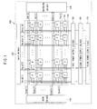
- FIG. 1 is a block diagram of organic light emitting display according to an embodiment of the invention.
- FIG. 2 is a circuit diagram of an pixel circuit employable by an organic light emitting display according to an embodiment of the present invention
- FIG. 3 is a timing diagram of signals employable to drive the pixel circuit of FIG. 2 ;
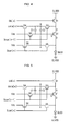
- FIG. 4 illustrates an operating state of the pixel circuit of FIG. 2 during an initialization period
- FIG. 5 illustrates an operating state of the pixel circuit of FIG. 2 during a threshold voltage compensating period
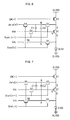
- FIG. 6 illustrates an operating state of the pixel circuit of FIG. 2 during a date write period and a voltage sensing period
- FIG. 7 illustrates an operating state of the pixel circuit of FIG. 2 during an emitting period
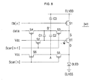
- FIG. 8 is a circuit diagram of another pixel circuit employable by an organic light emitting display according to another embodiment of the invention.
- FIG. 1 is a block diagram of an organic light emitting display 100, in the form of a flat panel display, according to the invention.
- the illustrated organic light emitting display 100 includes a scan driver 110, a data driver 120, an emission driver 130, an organic light emitting display panel 140 (hereinafter, a "panel"), a first power supply 150, a second power supply 160 and a third power supply 170.
- the scan driver 110 can sequentially apply a scan signal(s) to the panel 140 via a plurality of scan lines (Scan[1], Scan[2],....,Scan[n]).
- the data driver 120 can apply a data signal(s) to the panel 140 via a plurality of data lines (Data[1], Data[2],...., Data[m]).
- the emission driver 130 can sequentially apply emission signal(s) to the panel 140 via a plurality of emission lines (Em[1], Em[2], etc,Em[n]).
- the panel 140 includes a plurality of scan lines (Scan[1], Scan[2],....,Scan[n]) arranged in a column direction, a plurality of emission lines (Em[1], Em[2],...,Em[n]) arranged in a column direction, a plurality of data lines (Data[1], Data[2],....,Data[m]) arranged in a row direction, and a plurality of pixel circuits 141.
- the pixel circuits 141 are partially defined by respective portions of the plurality of scan lines (Scan[1], Scan[2], ..., and Scan [n]), the plurality of data lines (Data[1], Data[2], ..., and Data[m]) and the plurality of emission lines (Em[1], Em[2], ..., and Em[n]).
- each of the pixel circuits 141 is formed in a region defined by respective portions of two neighboring ones of the plurality of scan lines (Scan[1], Scan[2], ..., and Scan [n]) (or two neighboring ones of the plurality of emission lines (Em[1], Em[2], ..., and Em[n])) and two neighboring ones of the plurality of data lines (Data[1], Data[2], ..., and Data[m]).
- the pixel circuits 141 can be driven by respective ones of the plurality of scan lines (Scan[1], Scan[2],...,Scan[n]), the plurality of data lines (Data[1], Data[2],....,Data[m]), and the plurality of emission lines (Em[1], Em[2],...,Em[n]).
- a scan signal(s) output from the scan driver 110 can be applied to the respective one of the scan lines (Scan[1], Scan[2],....,Scan[n])
- a data signal(s) output from the data driver 120 can be applied to the respective one of the data lines (Data[1], Data[2],...., Data[m])
- an emission signal(s) output from the emission driver 130 can be applied to the respective one of the emission lines (Em[1], Em[2],....,Em[n]).
- the first power supply 150, the second power supply 160, and the third power supply 170 can respectively provide a first voltage ELVDD, a second voltage ELVSS, and a third voltage V dc to each of the pixel circuits 141 of the panel 140.
- FIG. 2 illustrates a circuit diagram of a pixel circuit 241 employable by an organic light emitting display according to the present invention.
- the pixel circuits 141 of the organic light emitting display of FIG. 1 may correspond to the pixel circuit 241 illustrated in FIG. 2 .
- the pixel circuit 241 is illustrated as being coupled to the nth scan line (Scan[n]), the mth data line (Data[m]) and the nth emission line (Em[n]) of the organic light emitting display 100 of FIG. 1 .
- the pixel circuit 241 is coupled to the nth emission line (EM[n]), a previous scan line (Scan[n-1]), the nth scan line (Scan[n]), the mth data line (Data[m]), the first power supply (ELVDD), the second power supply (ELVSS) and the third power supply (V dc ) of the display 100.
- the pixel circuit 241 includes a first switch S1, a second switch S2, a third switch S3, a fourth switch S4, a fifth switch S5, a sixth switch S6, a first capacitor C1, a second capacitor C2, a driving transistor DT, and an organic light emitting diode (OLED).
- the emission signal(s) supplied via the nth emission line (EM[n]) initialize the first and second capacitors C1, C2 and/or substantially and/or completely compensate for a threshold voltage of the driving transistor DT of the pixel circuit 241. Additionally, referring to FIG. 2 , in some embodiments with the emission line (EM[n]) electrically coupled to a control electrode of the first switch S1, the emission signal(s) supplied via the emission line (EM[n]) also controls an emission time of the OLED.
- the emission line (EM[n]) is at a low level
- the previous scan line (Scan[n-1]) is at a low level
- the scan line (Scan[n]) is at a high level
- the first and second capacitor C1, C2 are initialized to a value between the level of the first power supply (ELVDD) and the level of the third power supply (V dc ).
- the emission line (EM[n]) is electrically coupled to the emission driver 130 (see FIG. 1 ) for generating an emission signal(s) supplied thereto.
- the previous scan line (Scan[n-1]) can apply a previous scan signal, for selecting the previous scan line (Scan[n-1]) to the pixel 241 of the nth scan line (Scan[n]) during a previous (n-1)th scanning period.
- the previous scan line (Scan[n-1]) can apply the previous scan signal to a control electrode of the second switch S2 and a control electrode of the third switch S3 during the previous (n-1)th scanning period.
- a threshold voltage of the driving transistor DT is stored in the first and second capacitors C1, C2.
- the nth scan line (Scan[n]) can apply a respective scan signal(s) from the scan driver 110 (see FIG. 1 ) to select respective ones of the pixel circuits coupled to the nth scan line (Scan[n]) which are to emit light during an nth driving period. That is, during the nth driving period, OLEDs of the selected ones of the pixels circuits coupled to the nth scan line (Scan[n]) can emit light. More particularly, e.g., the pixel circuit 241 can be selected to emit light during a driving period by supplying the scan signal thereto. Referring to FIG.
- the nth scan line can apply a respective scan signal(s) to a control electrode of the fourth switch S4, a control electrode of the fifth switch S5, and a control electrode of the sixth switch S6.
- the nth scan signal can be described as 'supplied' when the scan signal has a low voltage level.
- the OLED thereof emits light during the respective driving period.
- nth scan signal when the nth scan signal is supplied to the nth scan line (Scan[n]), a data voltage from the mth data line (Data[m]) is stored in the first and second capacitors C1,C2, and simultaneously, a voltage (V EL ) of the OLED can be sensed and reflected.
- the nth scan line (Scan[n]) is electrically coupled to the scan driver 110, which may produce the respective scan signal(s).
- the mth data line (Data[m]) can apply a data signal (voltage), from the data driver 120 (see FIG. 1 ) to the first and second capacitors C1, C2 and the driving transistor DT.
- the voltage of the data signal is proportional or inversely proportional to a light emission brightness of the OLED of the pixel circuit 241.
- the mth data line (Data[m]) can be electrically coupled to the data driver 120 (see FIG. 1 ), which may produce the respective data signal(s).
- a first power line can enable the first voltage (ELVDD) to be applied to the OLED of the pixel circuit 241.
- the first power line can be coupled to the first power supply 150 (see FIG. 1 ), for supplying the first voltage (ELVDD).
- a second power line can enable the second voltage (ELVSS) to be applied to the OLED of the pixel circuit 241.
- the second power line can be coupled to the second power supply 160 (see FIG. 1 ), for supplying the second voltage (ELVSS).
- the first voltage (ELVDD) can be higher than the second voltage (ELVSS).
- a third power line can enable the third voltage (V dc ) to be applied to the first and second capacitors C1, C2 and a control electrode of the driving transistor DT.
- the third power line can be coupled to the third power supply 170 (see FIG. 1 ), for supplying the third voltage.
- the third voltage (V dc ) can be lower than the first voltage (ELVDD).
- the first switch S1 includes a control electrode (gate electrode) electrically coupled to the nth emission line (EM[n]), a first electrode (source electrode or drain electrode) electrically coupled to the first power line for receiving the first voltage (ELVDD), and a second electrode (the other of drain electrode or source electrode) electrically coupled to the driving transistor DT.
- EM[n] nth emission line
- first electrode source electrode or drain electrode
- second electrode the other of drain electrode or source electrode
- the second switch S2 includes a control electrode electrically coupled to the previous scan line (Scan[n-1]), a first electrode electrically coupled to the third power line for receiving the third voltage (V dc ), and a second electrode electrically coupled to the driving transistor DT.
- the third switch S3 includes a control electrode electrically coupled to the previous scan line (Scan[n-1]), a first electrode electrically coupled to the fourth switch S4, the first capacitor C1, and the second capacitor C2, and a second electrode electrically coupled to a node between the first switch S 1 and the driving transistor DT.
- the fourth switch S4 includes a control electrode electrically coupled to the nth scan line (Scan[n]), a first electrode electrically coupled to the data line (Data[m]), and a second electrode electrically coupled to the first capacitor C1, the second capacitor C2, and the third switch S3.
- the fifth switch S5 includes a control electrode electrically coupled to the nth scan line (Scan[n]), a first electrode electrically coupled to a node between the driving transistor DT and the OLED, and a second electrode electrically coupled to the sixth switch S6.
- the sixth switch S6 includes a control electrode electrically coupled to the scan line (Scan[n]), a first electrode electrically coupled to the third power line for supplying the third voltage (V dc ), and a second electrode electrically coupled to the fifth switch S5.
- the first capacitor C1 includes a first electrode electrically coupled to a node (B) between the second capacitor C2, the third switch S3, and the fourth switch S4, and a second electrode electrically coupled to the driving transistor DT and the second switch S2.
- the second capacitor C2 includes a first electrode electrically coupled to the node (B) between the first capacitor C1, the third switch S3, and the fourth switch S4, and a second electrode electrically coupled to a node (A) between the fifth switch S5 and the sixth switch S6.
- a first electrode of the driving transistor DT is electrically coupled to the first switch S 1 and the third switch S3 and a second electrode thereof is electrically coupled to the fifth switch S5 and the OLED.
- the control electrode of the driving transistor DT is electrically coupled to the first capacitor C1 and the second switch S2.
- the first, second, third, fourth, and fifth switches S1, S2, S3, S4, S5 and the driving transistor DT are illustrated as p-type transistors, e.g., p-channel field effect transistors, and the sixth switch S6 is illustrated as a n-type transistor, e.g., a n-channel field effect transistor.
- p-type transistors e.g., p-channel field effect transistors
- n-type transistor e.g., a n-channel field effect transistor.
- embodiments of the invention are not limited thereto.
- the driving transistor DT and/or the first, second, third, fourth and fifth switches S1, S2, S3, S4, S5, S6 may be any one selected from an amorphous silicon thin film transistor, a poly silicon thin film transistor, an organic thin film transistor, a micro thin film transistor, and equivalents thereof. However, embodiments of the invention are not limited thereto.
- the driving transistor DT and/or the switches S 1, S2, S3, S4, S5, S6 are poly silicon thin film transistors, they may be formed using, e.g., a laser crystallization method, a metal induction crystallization method, and equivalent methods thereof. However, embodiments of the invention are not limited thereto.
- the OLED includes an anode electrode electrically coupled to the driving transistor DT and the fifth switch S5, and a cathode electrode electrically coupled to the second power line for supplying the second voltage (ELVSS).
- the OLED emits lights of a predetermined brightness based on an amount of current controllably supplied thereto via the driving transistor DT.
- the OLED includes an emitting layer.
- the emitting layer may include, e.g., a low-polymer or a high-polymer.
- a low-polymer or a high-polymer.
- embodiments of the invention are not limited thereto. Because characteristics of a low-polymer material are widely known, it can be easily developed, and mass production is possible at an early stage.
- a high-polymer material may have excellent thermal stability, superior mechanical hardness, and a more-natural color as compared with a low-polymer material.
- FIG. 3 is a drive signal timing diagram illustrating signals employable to drive the pixel circuit 241 of FIG. 2 .
- a driving period for driving the pixel circuit 241 may include an initializing period (1), a threshold voltage compensating period (2), a data writing and OLED voltage sensing period (3), and an emitting period (4).
- FIG. 4 illustrates an operating state of the pixel circuit 241 of FIG. 2 during an initializing period (1).
- an emission signal at a low level is applied to the control electrode of the first switch S 1 via the nth emission line (EM[n]).
- a previous scan signal at a low level is applied to the control electrode of the second switch S2 and the control electrode of the third switch S3 via the previous scan line (Scan[n-1]).
- a scan signal at a high level is applied to the fourth switch S4, the fifth switch S5, and the sixth switch S6 via the scan line (Scan[n]).
- the first switch S1, the second switch S2, the third switch S3, and the sixth switch S6 are turned on while the fourth switch S4 and the fifth switch S5 are turned off.
- the first electrode of the first capacitor C1 is electrically coupled to the first power line for supplying the first voltage (ELVDD).
- the first electrode of the second capacitor C2 is also electrically coupled to the first power line for supplying the first voltage (ELVDD).
- the second electrode of the first capacitor C1 and the second electrode of the second capacitor C2 are electrically coupled to the third power line (V dc ).
- the control electrode of the driving transistor DT is also electrically coupled to the third power line (V dc ).
- a voltage of the control electrode of the driving transistor DT and a voltage of the first electrode of the driving transistor DT are determined by the following Equation Set 1.
- V G is a voltage of the control electrode of the driving transistor DT.
- V A is a voltage of node (A) between the second capacitor C2, the sixth switch S6 and the fifth switch S5.
- V dc is the third voltage supplied via the third power line.
- V S is a voltage of the first electrode of the driving transistor DT.
- V B is a voltage of node (B) between the third switch S3, the first capacitor C1, the second capacitor C2 and the fourth switch S4.
- ELVDD is the first voltage supplied via the first power line.
- FIG. 5 illustrates an operating state of the pixel circuit 241 of FIG. 2 during a threshold voltage compensating period (2).
- An emission signal at a high level is applied to the control electrode of the first switch S 1 via the nth emission line (EM[n]).
- a previous scan signal at a low level is applied to the control electrode of the second switch S2 and the control electrode of the third switch S3 via the previous scan line (Scan[n-1]).
- a scan signal at a high level is applied to the control electrodes of the fourth switch S4, the fifth switch S5 and the sixth switch S6 via the scan line (Scan[n]).
- the second switch S2, the third switch S3, and the sixth switch S6 are turned on while the first switch S1, the fourth switch S4, and the fifth switch S5 are turned off.
- the first electrode of the first capacitor C1 and the first electrode of the second capacitor C2 are electrically separated from the first power line for supplying the first voltage (ELVDD).
- the first electrode of the first capacitor C1 and the first electrode of the second capacitor C2 remain electrically coupled to the first electrode of the driving transistor DT via the third switch S3.
- the second electrode of the first capacitor C1 and the second electrode of the second capacitor C2 remain electrically coupled to the third power line (V dc ) via the second and sixth switches S2, S6, respectively.
- a voltage of the control electrode of the driving transistor DT and a voltage of the first electrode of the driving transistor are determined by the following Equation Set 2.
- a threshold voltage V th of the driving transistor DT is stored in the first capacitor C1 and the second capacitor C2.
- FIG. 6 illustrates an operating state of the pixel circuit 241 of FIG. 2 during a data writing and OLED voltage sensing period (3).
- an emission signal at a low level is applied to the control electrode of the first switch S1 via nth the emission line (EM[n]).
- a previous scan signal at a high level is applied to the control electrode of the second switch S2 and the control electrode of the third switch S3 via the previous scan line (Scan[n-1]).
- a scan signal at a low level is applied to the fourth switch S4, the fifth switch S5, and the sixth switch S6 via the nth scan line (Scan[n]).
- the first switch S1, the fourth switch S4, and the fifth switch S5 are turned on, and the second switch S2, the third switch S3, and the sixth switch S6 are turned off.
- the first electrode of the first capacitor C1 and the first electrode of the second capacitor C2 are electrically coupled to the mth data line (Data[m]).
- the second electrode of the first capacitor C1 is electrically coupled to the control electrode of the driving transistor DT, and the second electrode of the second capacitor C2 is electrically coupled to a node between the second electrode of the driving transistor DT and the anode electrode of the OLED via the fifth switch S5.
- V A V EL
- V B V data
- V EL is a voltage that may applied to the anode electrode of the OLED.
- V EL increases as a degradation level of the OLED increases.
- a voltage of the control electrode of the driving transistor DT are determined by the following Equation Set 4.
- V G V data -
- FIG. 7 illustrates an operating state of the pixel circuit 241 of FIG. 2 during an emitting period (4).
- an emission signal at a low level is applied to the control electrode of the first switch S1 via the nth emission line (EM[n]).
- a previous scan signal at a high level is applied to the control electrode of the second switch S2 and the control electrode of the third switch S3 via the previous scan line (Scan[n-1]).
- a scan signal at a high level is applied to the fourth switch S4, the fifth switch S5, and the sixth switch S6 via the nth scan line (Scan[n]).
- the first switch S1 and the sixth switch S6 are turned on, and the second switch S2, the third switch S3, the fourth switch S4, and the fifth switch S5 are turned off.
- the second electrode of the first capacitor C1 is electrically coupled to the control electrode of the driving transistor DT,
- the first electrode of the first capacitor C1 is electrically coupled to the first electrode of the second capacitor C2. That is, the first capacitor C1 is coupled to the second capacitor C2 in series.
- the second electrode of the second capacitor C2 is electrically coupled to the third power line for supplying the third voltage (V dc ).
- a voltage of node (A) changes and is determined by the following Equation 5.
- V A V dc
- a voltage of the control electrode of the driving transistor DT is determined by the following Equation Set 6.
- V G V data -
- + ⁇ V G ⁇ 2 ⁇ V G ⁇ 2 V dc - V EL
- V G V data -
- a current I OLED that may be supplied to the OLED in accordance with Equation Set 6 is determined by the following Equation 7.
- - V dc + V EL - Vth 2 ⁇ 2 ⁇ ELVDD - V data - V dc + V EL 2
- the more the voltage V EL of the OLED increases the more the current I OLED flowing through the OLED may increase. That is, in some embodiments, the current I OLED flowing through the OLED increases proportionally to the voltage V EL of the OLED.
- by increasing the voltage V EL of the OLED as the efficiency of the OLED decreases it is possible to substantially and/or completely suppress image sticking by increasing an amount of the current I OLED supplied to the OLED.
- some embodiments of the invention enable the lifetime of an organic light emitting display to be increased by controllably increasing the current I OLED supplied to the OLED as efficiency thereof decreases.
- a threshold voltage of the driving transistor DT is effectively stored effectively and substantially and/or completely compensated.
- FIG. 8 illustrates a circuit diagram of another pixel circuit 341 employable by an organic light emitting display according to another embodiment of the invention.
- One, some, or all of the pixel circuits 141 of the organic light emitting display of FIG. 1 may correspond to the pixel circuit 341 illustrated in FIG. 7 .
- the pixel circuit 341 is illustrated as being coupled to the nth scan line (Scan[n]), the mth data line (Data[m]) and the nth light emission control line (Em[n]) of the organic light emitting display 100 of FIG. 1 .
- the pixel circuit 341 has generally the same structure as the exemplary pixel circuit 241 of FIG. 2 . Only differences between the pixel circuit 341 of FIG. 8 and the pixel circuit 241 of FIG. 2 will be described below.
- the pixel circuit 341 includes a third capacitor C3 electrically coupled between the first power line for supplying the first voltage (ELVDD) and the second capacitor C2.
- a first electrode of the third capacitor C3 is electrically coupled to the first power line for supplying the first voltage (ELVDD).
- a second electrode of the third capacitor C3 is electrically coupled to a node (B') between the third switch S3, the fourth switch S4, the first capacitor C1, and the second capacitor C2.
- the third capacitor C3 serves to adjust a value of a voltage change due to a voltage V EL of the OLED and is employed in a feedback function. That is, in the pixel circuit 241 illustrated in FIG. 2 , because the voltage V EL of the OLED is fed back to the control electrode of the driving transistor DT, the current I OLED of the organic light emitting diode can increase excessively.
- a value of voltage change due to the voltage V EL of the OLED can controllably adjusted by the third capacitor C3 and feedback can be controllably executed. More particularly, in the pixel circuit 341 illustrated in FIG. 8 , the current provided to the OLED is determined by the following Equation 8. As may be seen from Equation 8, the voltage V EL of the OLED, for which a feedback operation is executed by the third capacitor C3, can be adjusted.
- Some embodiments may provide an organic light emitting display in which an increasing anode voltage of an OLED, which may be proportional to an amount of degradation of the OLED, may be sensed during a data writing period, and thus, an amount of current supplied to the OLED may be increased in proportion to the sensed voltage, such that image sticking and/or a reduction in a lifetime of the display due to degradation of the OLED may be substantially and/or completely suppressed.
- a storage capacitor may be electrically coupled to a node between a control electrode of a driving transistor and a first electrode of the driving transistor, and thus, a power source voltage provided to the first electrode thereof may be blocked, and a threshold voltage of the driving transistor may be stored naturally in the storage capacitor. That is, some embodiments of the present invention may compensate for a threshold voltage of the driving transistor without employing a diode-coupled structure.
Landscapes
- Engineering & Computer Science (AREA)
- Physics & Mathematics (AREA)
- Computer Hardware Design (AREA)
- General Physics & Mathematics (AREA)
- Theoretical Computer Science (AREA)
- Control Of Indicators Other Than Cathode Ray Tubes (AREA)
- Electroluminescent Light Sources (AREA)
- Control Of El Displays (AREA)
Abstract
Description
- The present invention relates to an organic light emitting display. More particularly, the invention relates to an organic light emitting display that can suppress image sticking due to a decrease in efficiency of an organic light emitting diode and can compensate for a threshold voltage of a drive transistor.
- In general, an organic light emitting display is a display that emits light by electrically exciting a fluorescent or phosphorescent compound. The organic light emitting display may display an image by driving N×M organic light emitting diodes (OLEDs). Each OLED may include an anode electrode (indium tin oxide (ITO)), an organic thin-film layer, and a cathode electrode (metal). To improve light emission efficiency and a balance between electrons and holes, the organic thin-film layer may have a multi-layer structure including an emitting layer (EML), an electron transport layer (ETL) and a hole transport layer (HTL). The organic thin-film may include a separate electron injecting layer (EIL) and a hole injecting layer (HIL).
- In general, the anode electrode is coupled to a first power supply to supply holes to the EML, and the cathode electrode is coupled with a second power supply to supply electrons to the EML. The second power supply has a lower voltage than the first power supply. Thus, relative to cathode electrode, the anode electrode has a positive (+) electric potential and, relative to the anode electrode, the cathode has a (-) electrode potential.
- The HTL accelerates hole(s) supplied from the anode electrode and supplies the hole(s) to the EML. The ETL accelerates electron(s) supplied from the cathode electrode and supplies the electron(s) to the EML. As a result, at the EML, the electron(s) supplied from the ETL and the hole(s) supplied from the HTL may recombine with each other, thereby generating a predetermined amount of light. The EML may include organic material that may generate one of red light (R), green light (G) and blue light (B) when the electron(s) and hole(s) recombine therein.
- In such OLEDs, because a voltage applied to the anode electrode is always higher than a voltage applied to the cathode electrode, negative (-) carriers are positioned on the anode electrode, and positive (+) carriers are positioned on the cathode electrode. If the negative (-) carriers positioned on the anode electrode and the positive (+) carriers positioned on the cathode electrode are maintained for a long time, movement of electron(s) and hole(s) can decrease. Thus, efficiency of the OLED(s) can decrease the more the OLED(s) is used. As a result, image sticking may occur and a life span of the OLED(s) can be shortened.
- The invention sets out to provide an organic light emitting display that substantially overcomes one or more of the problems due to the limitations and disadvantages of the related art.
- It is therefore an object of the invention to provide an organic light emitting display that may substantially and/or completely suppress an image sticking phenomenon and a reduction in a life time of the display as a result of degradation of organic light emitting diode(s) therein.
- It is a further object of the invention to provide an organic light emitting display that can compensate for a threshold voltage of a driving transistor of pixel circuit(s) thereof.
- At least one of the above and other features and advantages of the invention may be realized by providing an organic light emitting display, including a driving transistor electrically coupled to a first power line, a first switch electrically coupled to the driving transistor and an emission line, a second switch electrically coupled to the driving transistor and a previous scan line, a third switch electrically coupled to the first switch and a data line, a fourth switch electrically coupled to the data line and the third switch, a fifth switch electrically coupled to the driving transistor and a scan line, a first capacitor electrically coupled to the second switch and the third switch, a second capacitor electrically coupled to the third switch and the fifth switch, and an organic light emitting diode electrically coupled to the driving transistor and a second power line.
- The driving transistor may include a control electrode electrically coupled to the second switch, a first electrode electrically coupled to the first switch and the third switch, and a second electrode electrically coupled to the fifth switch and the organic light emitting diode. The first switch may include a control electrode electrically coupled to the emission line, a first electrode electrically coupled to the first power line, and a second electrode electrically coupled to the driving transistor. The second switch includes a control electrode electrically coupled to the previous scan line, a first electrode electrically coupled to a third power line, and a second electrode electrically coupled to the driving transistor.
- A voltage of the first power line is higher than a voltage of the third power line. The fourth switch may include a control electrode electrically coupled to the scan line, a first electrode electrically coupled to the data line, and a second electrode electrically coupled to the first capacitor, the second capacitor, and the third switch.
- The fifth switch may include a control electrode electrically coupled to the scan line, a first electrode electrically coupled to a node between the driving transistor and the organic light emitting diode. The sixth switch may be further electrically coupled to the fifth switch.
- The sixth switch may include a control electrode electrically coupled to the scan line, a first electrode electrically coupled to a third power line, and a second electrode electrically coupled to the fifth switch. The first switch, the second switch, the third switch, the fourth switch and the fifth switch may be P-channel field effect thin-film transistors and the sixth switch is a N-channel field effect thin-film transistor.
- The first capacitor may include a first electrode electrically coupled to the second capacitor, the third switch, and the fourth switch, and a second electrode electrically coupled to the driving transistor and the second switch. The second capacitor may include a first electrode electrically coupled to the first capacitor, the third switch, and the fourth switch, and a second electrode electrically coupled to the fifth switch.
- The organic light emitting diode may include an anode electrode electrically coupled to the driving transistor and the fifth switch, and a cathode electrode electrically coupled to the second power line.
- A third capacitor may be further electrically coupled to a node between the first power line and the first capacitor. The third capacitor may include a first electrode electrically coupled to the first power line and a second electrode electrically coupled to a node between the first capacitor, the second capacitor, the third switch, and the fourth switch.
- A voltage of the first power line may be higher than a voltage of the second power line. The third switch may include a control electrode electrically coupled to the previous scan line, a first electrode electrically coupled to a data line, the first capacitor, and the second capacitor, and a second electrode electrically coupled to a node between the first switch and the driving transistor. The fifth switch may be electrically coupled to the sixth switch, and the second switch and the sixth switch are electrically coupled to the third power line.
- When the previous scan line has a low level, the scan line has a high level, the emission line has a low level, a first electrode of the first capacitor, a first electrode of the second capacitor and a control electrode of the driving transistor are electrically coupled to a third power line, such that the first electrode of the first capacitor, the first electrode of the second capacitor and the control electrode of the driving transistor are initialized to a voltage level of the third power line.
- When the previous scan line is maintained at a low level, the scan line is maintained at a high level, and the emission line changes to a high level, a threshold voltage of the driving transistor may be reflected in the first and second capacitor, such that a voltage of the control electrode of the driving transistor has the voltage the level of the third power line, and the threshold voltage of the driving transistor is compensated.
- When the previous scan line changes to a high level, the scan line changes to a low level, and the emission line changes to a low level, a data voltage of the data line may be stored in the first and second capacitors and simultaneously, a threshold voltage of the organic light emitting diode is reflected.
- When the previous scan line is maintained at a high level, the scan line changes to a high level and the emission line is maintained at a low level, current provided to the organic light emitting diode through the driving transistor may increase due to the data voltage and the threshold voltage of the organic light emitting diode reflected in the first and second capacitor.
- The current provided to the organic light emitting diode may increase in proportion to the threshold voltage of the organic light emitting diode.
- The above and other features and advantages of the present invention will become more apparent to those of ordinary skill in the art upon making reference to the following description of embodiments thereof which is given with reference to the attached drawings, in which:
-
FIG. 1 is a block diagram of organic light emitting display according to an embodiment of the invention; -
FIG. 2 is a circuit diagram of an pixel circuit employable by an organic light emitting display according to an embodiment of the present invention; -
FIG. 3 is a timing diagram of signals employable to drive the pixel circuit ofFIG. 2 ; -
FIG. 4 illustrates an operating state of the pixel circuit ofFIG. 2 during an initialization period; -
FIG. 5 illustrates an operating state of the pixel circuit ofFIG. 2 during a threshold voltage compensating period; -
FIG. 6 illustrates an operating state of the pixel circuit ofFIG. 2 during a date write period and a voltage sensing period; -
FIG. 7 illustrates an operating state of the pixel circuit ofFIG. 2 during an emitting period; and -
FIG. 8 is a circuit diagram of another pixel circuit employable by an organic light emitting display according to another embodiment of the invention. - Embodiments of the invention will now be described more fully hereinafter with reference to the accompanying drawings. The invention may, however, be embodied in different forms and should not be construed as limited to the embodiments set forth herein. Rather, these embodiments are provided so that this disclosure will be thorough and complete, and will clearly convey the nature of the invention to those skilled in the art.
- Elements having similar constitutions and/or operations are denoted by the same and/or like reference numerals throughout the specification. Furthermore, it should be understood that electrical coupling between a certain component and another component includes direct electrical coupling between them as well as indirect electrical coupling between them by an interposed component. It will also be understood that, unless specified otherwise, when an element is referred to as being "between" two elements, it can be the only element between the two elements, or one or more intervening elements may also be present.
-
FIG. 1 is a block diagram of an organiclight emitting display 100, in the form of a flat panel display, according to the invention. - Referring to
FIG. 1 , the illustrated organiclight emitting display 100 includes ascan driver 110, adata driver 120, anemission driver 130, an organic light emitting display panel 140 (hereinafter, a "panel"), afirst power supply 150, asecond power supply 160 and athird power supply 170. - The
scan driver 110 can sequentially apply a scan signal(s) to thepanel 140 via a plurality of scan lines (Scan[1], Scan[2],....,Scan[n]). - The
data driver 120 can apply a data signal(s) to thepanel 140 via a plurality of data lines (Data[1], Data[2],...., Data[m]). - The
emission driver 130 can sequentially apply emission signal(s) to thepanel 140 via a plurality of emission lines (Em[1], Em[2],.....,Em[n]). - The
panel 140 includes a plurality of scan lines (Scan[1], Scan[2],....,Scan[n]) arranged in a column direction, a plurality of emission lines (Em[1], Em[2],...,Em[n]) arranged in a column direction, a plurality of data lines (Data[1], Data[2],....,Data[m]) arranged in a row direction, and a plurality ofpixel circuits 141. - The
pixel circuits 141 are partially defined by respective portions of the plurality of scan lines (Scan[1], Scan[2], ..., and Scan [n]), the plurality of data lines (Data[1], Data[2], ..., and Data[m]) and the plurality of emission lines (Em[1], Em[2], ..., and Em[n]). More particularly, each of thepixel circuits 141 is formed in a region defined by respective portions of two neighboring ones of the plurality of scan lines (Scan[1], Scan[2], ..., and Scan [n]) (or two neighboring ones of the plurality of emission lines (Em[1], Em[2], ..., and Em[n])) and two neighboring ones of the plurality of data lines (Data[1], Data[2], ..., and Data[m]). - The
pixel circuits 141 can be driven by respective ones of the plurality of scan lines (Scan[1], Scan[2],...,Scan[n]), the plurality of data lines (Data[1], Data[2],....,Data[m]), and the plurality of emission lines (Em[1], Em[2],...,Em[n]). As described above, a scan signal(s) output from thescan driver 110 can be applied to the respective one of the scan lines (Scan[1], Scan[2],....,Scan[n]), a data signal(s) output from thedata driver 120 can be applied to the respective one of the data lines (Data[1], Data[2],...., Data[m]), and an emission signal(s) output from theemission driver 130 can be applied to the respective one of the emission lines (Em[1], Em[2],....,Em[n]). - The
first power supply 150, thesecond power supply 160, and thethird power supply 170 can respectively provide a first voltage ELVDD, a second voltage ELVSS, and a third voltage Vdc to each of thepixel circuits 141 of thepanel 140. -
FIG. 2 illustrates a circuit diagram of apixel circuit 241 employable by an organic light emitting display according to the present invention. For example, one, some or all of thepixel circuits 141 of the organic light emitting display ofFIG. 1 may correspond to thepixel circuit 241 illustrated inFIG. 2 . For ease of description, thepixel circuit 241 is illustrated as being coupled to the nth scan line (Scan[n]), the mth data line (Data[m]) and the nth emission line (Em[n]) of the organiclight emitting display 100 ofFIG. 1 . - More particularly, referring to
FIG. 2 , thepixel circuit 241 is coupled to the nth emission line (EM[n]), a previous scan line (Scan[n-1]), the nth scan line (Scan[n]), the mth data line (Data[m]), the first power supply (ELVDD), the second power supply (ELVSS) and the third power supply (Vdc) of thedisplay 100. Thepixel circuit 241 includes a first switch S1, a second switch S2, a third switch S3, a fourth switch S4, a fifth switch S5, a sixth switch S6, a first capacitor C1, a second capacitor C2, a driving transistor DT, and an organic light emitting diode (OLED). - As described in more detail below, the emission signal(s) supplied via the nth emission line (EM[n]) initialize the first and second capacitors C1, C2 and/or substantially and/or completely compensate for a threshold voltage of the driving transistor DT of the
pixel circuit 241. Additionally, referring toFIG. 2 , in some embodiments with the emission line (EM[n]) electrically coupled to a control electrode of the first switch S1, the emission signal(s) supplied via the emission line (EM[n]) also controls an emission time of the OLED. As one example, if the emission line (EM[n]) is at a low level, the previous scan line (Scan[n-1]) is at a low level, and the scan line (Scan[n]) is at a high level, the first and second capacitor C1, C2 are initialized to a value between the level of the first power supply (ELVDD) and the level of the third power supply (Vdc). As described above, the emission line (EM[n]) is electrically coupled to the emission driver 130 (seeFIG. 1 ) for generating an emission signal(s) supplied thereto. - The previous scan line (Scan[n-1]) can apply a previous scan signal, for selecting the previous scan line (Scan[n-1]) to the
pixel 241 of the nth scan line (Scan[n]) during a previous (n-1)th scanning period. Referring toFIG. 2 , the previous scan line (Scan[n-1]) can apply the previous scan signal to a control electrode of the second switch S2 and a control electrode of the third switch S3 during the previous (n-1)th scanning period. If the previous scan signal supplied to the previous scan line (Scan[n-1]) is at a low level while the emission line (EM[n]) is at a high level, and the scan line (Scan[n]) is at a high level, a threshold voltage of the driving transistor DT is stored in the first and second capacitors C1, C2. - The nth scan line (Scan[n]) can apply a respective scan signal(s) from the scan driver 110 (see
FIG. 1 ) to select respective ones of the pixel circuits coupled to the nth scan line (Scan[n]) which are to emit light during an nth driving period. That is, during the nth driving period, OLEDs of the selected ones of the pixels circuits coupled to the nth scan line (Scan[n]) can emit light. More particularly, e.g., thepixel circuit 241 can be selected to emit light during a driving period by supplying the scan signal thereto. Referring toFIG. 2 , the nth scan line (Scan[n]) can apply a respective scan signal(s) to a control electrode of the fourth switch S4, a control electrode of the fifth switch S5, and a control electrode of the sixth switch S6. For example, in embodiments in which the fourth switch S4 and the fifth switch S5 are p-type transistors, the nth scan signal can be described as 'supplied' when the scan signal has a low voltage level. When the nth scan signal is supplied to thepixel circuit 241, the OLED thereof emits light during the respective driving period. More particularly, when the nth scan signal is supplied to the nth scan line (Scan[n]), a data voltage from the mth data line (Data[m]) is stored in the first and second capacitors C1,C2, and simultaneously, a voltage (VEL) of the OLED can be sensed and reflected. The nth scan line (Scan[n]) is electrically coupled to thescan driver 110, which may produce the respective scan signal(s). - The mth data line (Data[m]) can apply a data signal (voltage), from the data driver 120 (see
FIG. 1 ) to the first and second capacitors C1, C2 and the driving transistor DT. The voltage of the data signal is proportional or inversely proportional to a light emission brightness of the OLED of thepixel circuit 241. The mth data line (Data[m]) can be electrically coupled to the data driver 120 (seeFIG. 1 ), which may produce the respective data signal(s). - A first power line can enable the first voltage (ELVDD) to be applied to the OLED of the
pixel circuit 241. The first power line can be coupled to the first power supply 150 (seeFIG. 1 ), for supplying the first voltage (ELVDD). - A second power line can enable the second voltage (ELVSS) to be applied to the OLED of the
pixel circuit 241. The second power line can be coupled to the second power supply 160 (seeFIG. 1 ), for supplying the second voltage (ELVSS). The first voltage (ELVDD) can be higher than the second voltage (ELVSS). - A third power line can enable the third voltage (Vdc) to be applied to the first and second capacitors C1, C2 and a control electrode of the driving transistor DT. The third power line can be coupled to the third power supply 170 (see
FIG. 1 ), for supplying the third voltage. The third voltage (Vdc) can be lower than the first voltage (ELVDD). - Referring to
FIG. 2 , the first switch S1 includes a control electrode (gate electrode) electrically coupled to the nth emission line (EM[n]), a first electrode (source electrode or drain electrode) electrically coupled to the first power line for receiving the first voltage (ELVDD), and a second electrode (the other of drain electrode or source electrode) electrically coupled to the driving transistor DT. - The second switch S2 includes a control electrode electrically coupled to the previous scan line (Scan[n-1]), a first electrode electrically coupled to the third power line for receiving the third voltage (Vdc), and a second electrode electrically coupled to the driving transistor DT.
- The third switch S3 includes a control electrode electrically coupled to the previous scan line (Scan[n-1]), a first electrode electrically coupled to the fourth switch S4, the first capacitor C1, and the second capacitor C2, and a second electrode electrically coupled to a node between the
first switch S 1 and the driving transistor DT. - The fourth switch S4 includes a control electrode electrically coupled to the nth scan line (Scan[n]), a first electrode electrically coupled to the data line (Data[m]), and a second electrode electrically coupled to the first capacitor C1, the second capacitor C2, and the third switch S3.
- The fifth switch S5 includes a control electrode electrically coupled to the nth scan line (Scan[n]), a first electrode electrically coupled to a node between the driving transistor DT and the OLED, and a second electrode electrically coupled to the sixth switch S6.
- The sixth switch S6 includes a control electrode electrically coupled to the scan line (Scan[n]), a first electrode electrically coupled to the third power line for supplying the third voltage (Vdc), and a second electrode electrically coupled to the fifth switch S5.
- As described above, when a scan signal of a low level is applied to the
pixel circuit 241 via the nth scan line (Scan[n]), the fourth switch S4 and the fifth switch S5 are turned on, and the sixth switch S6 is turned off. When a scan signal of a high level is applied to thepixel circuit 241 via the scan line (Scan[n]), the fourth switch S4 and the fifth switch S5 are turned off, and the sixth switch S6 is turned on. - The first capacitor C1 includes a first electrode electrically coupled to a node (B) between the second capacitor C2, the third switch S3, and the fourth switch S4, and a second electrode electrically coupled to the driving transistor DT and the second switch S2.
- The second capacitor C2 includes a first electrode electrically coupled to the node (B) between the first capacitor C1, the third switch S3, and the fourth switch S4, and a second electrode electrically coupled to a node (A) between the fifth switch S5 and the sixth switch S6.
- A first electrode of the driving transistor DT is electrically coupled to the
first switch S 1 and the third switch S3 and a second electrode thereof is electrically coupled to the fifth switch S5 and the OLED. The control electrode of the driving transistor DT is electrically coupled to the first capacitor C1 and the second switch S2. - In the embodiment illustrated in
FIG. 2 , the first, second, third, fourth, and fifth switches S1, S2, S3, S4, S5 and the driving transistor DT are illustrated as p-type transistors, e.g., p-channel field effect transistors, and the sixth switch S6 is illustrated as a n-type transistor, e.g., a n-channel field effect transistor. However, embodiments of the invention are not limited thereto. - The driving transistor DT and/or the first, second, third, fourth and fifth switches S1, S2, S3, S4, S5, S6 may be any one selected from an amorphous silicon thin film transistor, a poly silicon thin film transistor, an organic thin film transistor, a micro thin film transistor, and equivalents thereof. However, embodiments of the invention are not limited thereto.
- If the driving transistor DT and/or the
switches S 1, S2, S3, S4, S5, S6 are poly silicon thin film transistors, they may be formed using, e.g., a laser crystallization method, a metal induction crystallization method, and equivalent methods thereof. However, embodiments of the invention are not limited thereto. - The OLED includes an anode electrode electrically coupled to the driving transistor DT and the fifth switch S5, and a cathode electrode electrically coupled to the second power line for supplying the second voltage (ELVSS). The OLED emits lights of a predetermined brightness based on an amount of current controllably supplied thereto via the driving transistor DT.
- The OLED includes an emitting layer. The emitting layer may include, e.g., a low-polymer or a high-polymer. However, embodiments of the invention are not limited thereto. Because characteristics of a low-polymer material are widely known, it can be easily developed, and mass production is possible at an early stage. A high-polymer material may have excellent thermal stability, superior mechanical hardness, and a more-natural color as compared with a low-polymer material.
-
FIG. 3 is a drive signal timing diagram illustrating signals employable to drive thepixel circuit 241 ofFIG. 2 . - As illustrated in
FIG. 3 , a driving period for driving thepixel circuit 241 may include an initializing period (①), a threshold voltage compensating period (②), a data writing and OLED voltage sensing period (③), and an emitting period (④). - The operation of the
pixel circuit 241 in accordance with the invention will be described with reference toFIGS. 2 through 7 . -
FIG. 4 illustrates an operating state of thepixel circuit 241 ofFIG. 2 during an initializing period (①). - During the initializing period (①), an emission signal at a low level is applied to the control electrode of the
first switch S 1 via the nth emission line (EM[n]). A previous scan signal at a low level is applied to the control electrode of the second switch S2 and the control electrode of the third switch S3 via the previous scan line (Scan[n-1]). A scan signal at a high level is applied to the fourth switch S4, the fifth switch S5, and the sixth switch S6 via the scan line (Scan[n]). - Therefore, during the initializing period (①), the first switch S1, the second switch S2, the third switch S3, and the sixth switch S6 are turned on while the fourth switch S4 and the fifth switch S5 are turned off.
- Accordingly, the first electrode of the first capacitor C1 is electrically coupled to the first power line for supplying the first voltage (ELVDD). The first electrode of the second capacitor C2 is also electrically coupled to the first power line for supplying the first voltage (ELVDD). The second electrode of the first capacitor C1 and the second electrode of the second capacitor C2 are electrically coupled to the third power line (Vdc). The control electrode of the driving transistor DT is also electrically coupled to the third power line (Vdc).
- During the initializing period (①), a voltage of the control electrode of the driving transistor DT and a voltage of the first electrode of the driving transistor DT are determined by the following
Equation Set 1.
- Further, VS is a voltage of the first electrode of the driving transistor DT. VB is a voltage of node (B) between the third switch S3, the first capacitor C1, the second capacitor C2 and the fourth switch S4. ELVDD is the first voltage supplied via the first power line.
-
FIG. 5 illustrates an operating state of thepixel circuit 241 ofFIG. 2 during a threshold voltage compensating period (②). - An emission signal at a high level is applied to the control electrode of the
first switch S 1 via the nth emission line (EM[n]). A previous scan signal at a low level is applied to the control electrode of the second switch S2 and the control electrode of the third switch S3 via the previous scan line (Scan[n-1]). A scan signal at a high level is applied to the control electrodes of the fourth switch S4, the fifth switch S5 and the sixth switch S6 via the scan line (Scan[n]). - Therefore, during the threshold voltage compensating period (②), the second switch S2, the third switch S3, and the sixth switch S6 are turned on while the first switch S1, the fourth switch S4, and the fifth switch S5 are turned off.
- Accordingly, the first electrode of the first capacitor C1 and the first electrode of the second capacitor C2 are electrically separated from the first power line for supplying the first voltage (ELVDD). The first electrode of the first capacitor C1 and the first electrode of the second capacitor C2 remain electrically coupled to the first electrode of the driving transistor DT via the third switch S3. The second electrode of the first capacitor C1 and the second electrode of the second capacitor C2 remain electrically coupled to the third power line (Vdc) via the second and sixth switches S2, S6, respectively.
- Under such conditions, voltages of the first electrode of the first capacitor C1, the first electrode of the second capacitor C2, and the first electrode of the driving transistor DT fall from the first voltage (ELVDD), but do not fall below the threshold voltage of the driving transistor DT.
- That is, during the threshold voltage compensating period (②), a voltage of the control electrode of the driving transistor DT and a voltage of the first electrode of the driving transistor are determined by the following
Equation Set 2.
- That is, during a threshold voltage compensating period (②), because the node (B) is electrically separated from the first power line for supplying the first voltage (ELVDD), a voltage VB at the node (B) continues to fall, but does not fall below a threshold voltage Vth of the driving transistor DT. Accordingly, a threshold voltage Vth of the driving transistor DT is stored in the first capacitor C1 and the second capacitor C2.
-
FIG. 6 illustrates an operating state of thepixel circuit 241 ofFIG. 2 during a data writing and OLED voltage sensing period (③). - During the data writing and OLED voltage sensing period (③), an emission signal at a low level is applied to the control electrode of the first switch S1 via nth the emission line (EM[n]). A previous scan signal at a high level is applied to the control electrode of the second switch S2 and the control electrode of the third switch S3 via the previous scan line (Scan[n-1]). A scan signal at a low level is applied to the fourth switch S4, the fifth switch S5, and the sixth switch S6 via the nth scan line (Scan[n]).
- Therefore, during the data writing and OLED voltage sensing period (③), the first switch S1, the fourth switch S4, and the fifth switch S5 are turned on, and the second switch S2, the third switch S3, and the sixth switch S6 are turned off.
- Accordingly, during the data writing and OLED voltage sensing period (③), the first electrode of the first capacitor C1 and the first electrode of the second capacitor C2 are electrically coupled to the mth data line (Data[m]). The second electrode of the first capacitor C1 is electrically coupled to the control electrode of the driving transistor DT, and the second electrode of the second capacitor C2 is electrically coupled to a node between the second electrode of the driving transistor DT and the anode electrode of the OLED via the fifth switch S5.
- Accordingly, during the data writing and OLED voltage sensing period (③), voltages of the node (A) and the node (B) change. More particularly, during the data writing and OLED voltage sensing period (③), the voltages of the node (A) and the node (B) are determined by the following
Equation Set 3.
- Further, in some embodiments, a voltage of the control electrode of the driving transistor DT are determined by the following
Equation Set 4.
-
FIG. 7 illustrates an operating state of thepixel circuit 241 ofFIG. 2 during an emitting period (④).
During the emitting period (④), an emission signal at a low level is applied to the control electrode of the first switch S1 via the nth emission line (EM[n]). A previous scan signal at a high level is applied to the control electrode of the second switch S2 and the control electrode of the third switch S3 via the previous scan line (Scan[n-1]). A scan signal at a high level is applied to the fourth switch S4, the fifth switch S5, and the sixth switch S6 via the nth scan line (Scan[n]). - Therefore, during the emitting period (④), the first switch S1 and the sixth switch S6 are turned on, and the second switch S2, the third switch S3, the fourth switch S4, and the fifth switch S5 are turned off.
- Accordingly, during the emitting period (④), the second electrode of the first capacitor C1 is electrically coupled to the control electrode of the driving transistor DT, The first electrode of the first capacitor C1 is electrically coupled to the first electrode of the second capacitor C2. That is, the first capacitor C1 is coupled to the second capacitor C2 in series. The second electrode of the second capacitor C2 is electrically coupled to the third power line for supplying the third voltage (Vdc).
- During the emitting period (④), a voltage of node (A) changes and is determined by the following
Equation 5.
- A voltage of the control electrode of the driving transistor DT is determined by the following
Equation Set 6.
- During the emitting period (④), a current IOLED that may be supplied to the OLED in accordance with
Equation Set 6 is determined by the following Equation 7.
- As may be seen in Equation 7, in some embodiments of the invention, the more the voltage VEL of the OLED increases, the more the current IOLED flowing through the OLED may increase. That is, in some embodiments, the current IOLED flowing through the OLED increases proportionally to the voltage VEL of the OLED. In some embodiments, by increasing the voltage VEL of the OLED as the efficiency of the OLED decreases, it is possible to substantially and/or completely suppress image sticking by increasing an amount of the current IOLED supplied to the OLED. As a result, some embodiments of the invention enable the lifetime of an organic light emitting display to be increased by controllably increasing the current IOLED supplied to the OLED as efficiency thereof decreases. Further, in some embodiments of the invention, a threshold voltage of the driving transistor DT is effectively stored effectively and substantially and/or completely compensated.
-
FIG. 8 illustrates a circuit diagram of anotherpixel circuit 341 employable by an organic light emitting display according to another embodiment of the invention. One, some, or all of thepixel circuits 141 of the organic light emitting display ofFIG. 1 may correspond to thepixel circuit 341 illustrated inFIG. 7 . For ease of description, thepixel circuit 341 is illustrated as being coupled to the nth scan line (Scan[n]), the mth data line (Data[m]) and the nth light emission control line (Em[n]) of the organiclight emitting display 100 ofFIG. 1 . - As shown in
FIG. 8 , thepixel circuit 341 has generally the same structure as theexemplary pixel circuit 241 ofFIG. 2 . Only differences between thepixel circuit 341 ofFIG. 8 and thepixel circuit 241 ofFIG. 2 will be described below. Referring toFIG. 8 , thepixel circuit 341 includes a third capacitor C3 electrically coupled between the first power line for supplying the first voltage (ELVDD) and the second capacitor C2. A first electrode of the third capacitor C3 is electrically coupled to the first power line for supplying the first voltage (ELVDD). A second electrode of the third capacitor C3 is electrically coupled to a node (B') between the third switch S3, the fourth switch S4, the first capacitor C1, and the second capacitor C2. - The third capacitor C3 serves to adjust a value of a voltage change due to a voltage VEL of the OLED and is employed in a feedback function. That is, in the
pixel circuit 241 illustrated inFIG. 2 , because the voltage VEL of the OLED is fed back to the control electrode of the driving transistor DT, the current IOLED of the organic light emitting diode can increase excessively. - However, in the
pixel circuit 341 illustrated inFIG. 8 , a value of voltage change due to the voltage VEL of the OLED can controllably adjusted by the third capacitor C3 and feedback can be controllably executed. More particularly, in thepixel circuit 341 illustrated inFIG. 8 , the current provided to the OLED is determined by the following Equation 8. As may be seen from Equation 8, the voltage VEL of the OLED, for which a feedback operation is executed by the third capacitor C3, can be adjusted.
- Some embodiments may provide an organic light emitting display in which an increasing anode voltage of an OLED, which may be proportional to an amount of degradation of the OLED, may be sensed during a data writing period, and thus, an amount of current supplied to the OLED may be increased in proportion to the sensed voltage, such that image sticking and/or a reduction in a lifetime of the display due to degradation of the OLED may be substantially and/or completely suppressed.
- Further, in some embodiments of an organic light emitting display according to the invention, a storage capacitor may be electrically coupled to a node between a control electrode of a driving transistor and a first electrode of the driving transistor, and thus, a power source voltage provided to the first electrode thereof may be blocked, and a threshold voltage of the driving transistor may be stored naturally in the storage capacitor. That is, some embodiments of the present invention may compensate for a threshold voltage of the driving transistor without employing a diode-coupled structure.
- Certain embodiments of the present invention have been disclosed herein, and although specific terms are employed, they are used and are to be interpreted in a generic and descriptive sense only and not for purpose of limitation. Accordingly, it will be understood by those of ordinary skill in the art that various changes in form and details may be made without departing from the scope of the present invention as set forth in the following claims.
Claims (23)
- An organic light emitting display, comprising:a driving transistor electrically coupled to a first power line;a first switch electrically coupled to the driving transistor and an emission line;a second switch electrically coupled to the driving transistor and a previous scan line;a third switch electrically coupled to the first switch and a data line;a fourth switch electrically coupled to the data line and the third switch;a fifth switch electrically coupled to the driving transistor and a scan line;a first capacitor electrically coupled to the second switch and the third switch;a second capacitor electrically coupled to the third switch and the fifth switch; andan organic light emitting diode electrically coupled to the driving transistor and a second power line.
- An organic light emitting display as claimed in claim 1, wherein the driving transistor includes a control electrode electrically coupled to the second switch, a first electrode electrically coupled to the first switch and the third switch, and a second electrode electrically coupled to the fifth switch and the organic light emitting diode.
- An organic light emitting display as claimed in claim 1 or 2, wherein the first switch includes a control electrode electrically coupled to the emission line, a first electrode electrically coupled to the first power line, and a second electrode electrically coupled to the driving transistor.
- An organic light emitting display as claimed in any preceding claim, wherein the second switch includes a control electrode electrically coupled to the previous scan line, a first electrode electrically coupled to a third power line, and a second electrode electrically coupled to the driving transistor.
- An organic light emitting display as claimed in any preceding claim, wherein a voltage of the first power line is higher than a voltage of the third power line.
- An organic light emitting display as claimed in any preceding claim, wherein the fourth switch includes a control electrode electrically coupled to the scan line, a first electrode electrically coupled to the data line, and a second electrode electrically coupled to the first capacitor, the second capacitor, and the third switch.
- An organic light emitting display as claimed in any preceding claim, wherein the fifth switch includes a control electrode electrically coupled to the scan line, and a first electrode electrically coupled to a node between the driving transistor and the organic light emitting diode.
- An organic light emitting display as claimed in any preceding claim, wherein the sixth switch is further electrically coupled to the fifth switch.
- An organic light emitting display as claimed in any preceding claim, wherein the sixth switch includes a control electrode electrically coupled to the scan line, a first electrode electrically coupled to a third power line, and a second electrode electrically coupled to the fifth switch.
- An organic light emitting display as claimed in any preceding claim, wherein the first switch, the second switch, the third switch, the fourth switch, and the fifth switch are P-channel field effect thin-film transistors, and the sixth switch is a N-channel field effect thin-film transistor.
- An organic light emitting display as claimed in any preceding claim, wherein the first capacitor includes a first electrode electrically coupled to the second capacitor, the third switch, and the fourth switch, and a second electrode electrically coupled to the driving transistor and the second switch.
- An organic light emitting display as claimed in any preceding claim, wherein the second capacitor includes a first electrode electrically coupled to the first capacitor, the third switch, and the fourth switch, and a second electrode electrically coupled to the fifth switch.
- An organic light emitting display as claimed in any preceding claim, wherein the organic light emitting diode includes an anode electrode electrically coupled to the driving transistor and the fifth switch, and a cathode electrode electrically coupled to the second power line.
- An organic light emitting display as claimed in any preceding claim, wherein a third capacitor is further electrically coupled between the first power line and the first capacitor.
- An organic light emitting display as claimed in any preceding claim, wherein the third capacitor includes a first electrode electrically coupled to the first power line and a second electrode electrically coupled to a node between the first capacitor, the second capacitor, the third switch, and the fourth switch.
- An organic light emitting display as claimed in any preceding claim, wherein a voltage of the first power line is higher than a voltage of the second power line.
- An organic light emitting display as claimed in any preceding claim, wherein the third switch includes a control electrode electrically coupled to the previous scan line, a first electrode electrically coupled to a data line, the first capacitor, and the second capacitor, and a second electrode electrically coupled to a node between the first switch and the driving transistor.
- An organic light emitting display as claimed in any preceding claim, wherein:the fifth switch is electrically coupled to the sixth switch, andthe second switch and the sixth switch are electrically coupled to the third power line.
- An organic light emitting display as claimed in claim 18, wherein when the previous scan line has a low level, the scan line has a high level, the emission line has a low level, a second electrode of the first capacitor, a second electrode of the second capacitor and a control electrode of the driving transistor are electrically coupled to a third power line, such that the second electrode of the first capacitor, the second electrode of the second capacitor and the control electrode of the driving transistor are initialized to a voltage level of the third power line.
- An organic light emitting display as claimed in claim 19, wherein when the previous scan line is maintained at a low level, the scan line is maintained at a high level, and the emission line changes to a high level, a threshold voltage of the driving transistor is reflected in the first and second capacitor, such that a voltage of the control electrode of the driving transistor has the voltage the level of the third power line, and the threshold voltage of the driving transistor is compensated.
- An organic light emitting display as claimed in claim 20, wherein when the previous scan line changes to a high level, the scan line changes to a low level, and the emission line changes to a low level, a data voltage of the data line is stored in the first and second capacitors and simultaneously, an anode voltage of the organic light emitting diode is reflected.
- An organic light emitting display as claimed in claim 21, wherein when the previous scan line is maintained at a high level, the scan line changes to a high level and the emission line is maintained at a low level, current provided to the organic light emitting diode through the driving transistor increases due to the data voltage and the anode voltage of the organic light emitting diode reflected in the first and second capacitor.
- An organic light emitting display as claimed in claim 22, wherein the current provided to the organic light emitting diode increases in proportion to the anode voltage of the organic light emitting diode.
Applications Claiming Priority (1)
| Application Number | Priority Date | Filing Date | Title |
|---|---|---|---|
| KR1020070020802A KR100865396B1 (en) | 2007-03-02 | 2007-03-02 | Organic electroluminescent display |
Publications (1)
| Publication Number | Publication Date |
|---|---|
| EP1968039A1 true EP1968039A1 (en) | 2008-09-10 |
Family
ID=39319619
Family Applications (1)
| Application Number | Title | Priority Date | Filing Date |
|---|---|---|---|
| EP08250708A Ceased EP1968039A1 (en) | 2007-03-02 | 2008-02-29 | Organic light emitting display |
Country Status (5)
| Country | Link |
|---|---|
| US (1) | US8120556B2 (en) |
| EP (1) | EP1968039A1 (en) |
| JP (1) | JP5038167B2 (en) |
| KR (1) | KR100865396B1 (en) |
| CN (1) | CN101256737B (en) |
Cited By (3)
| Publication number | Priority date | Publication date | Assignee | Title |
|---|---|---|---|---|
| US8149186B2 (en) | 2007-04-10 | 2012-04-03 | Samsung Mobile Display Co., Ltd. | Pixel, organic light emitting display using the same, and associated methods |
| US8194012B2 (en) | 2008-03-10 | 2012-06-05 | Samsung Mobile Display Co.,Ltd. | Pixel and organic light emitting display using the same |
| CN106782323A (en) * | 2017-02-15 | 2017-05-31 | 京东方科技集团股份有限公司 | Pixel-driving circuit and its driving method, display device |
Families Citing this family (42)
| Publication number | Priority date | Publication date | Assignee | Title |
|---|---|---|---|---|
| KR100986896B1 (en) | 2008-12-05 | 2010-10-08 | 삼성모바일디스플레이주식회사 | Organic light emitting display device and driving method thereof |
| US9740341B1 (en) | 2009-02-26 | 2017-08-22 | Amazon Technologies, Inc. | Capacitive sensing with interpolating force-sensitive resistor array |
| US10180746B1 (en) * | 2009-02-26 | 2019-01-15 | Amazon Technologies, Inc. | Hardware enabled interpolating sensor and display |
| US9785272B1 (en) | 2009-07-31 | 2017-10-10 | Amazon Technologies, Inc. | Touch distinction |
| US9740340B1 (en) | 2009-07-31 | 2017-08-22 | Amazon Technologies, Inc. | Visually consistent arrays including conductive mesh |
| KR101056308B1 (en) * | 2009-10-19 | 2011-08-11 | 삼성모바일디스플레이주식회사 | Organic light emitting display device and driving method thereof |
| KR101113430B1 (en) * | 2009-12-10 | 2012-03-02 | 삼성모바일디스플레이주식회사 | Pixel and organic light emitting display device using the same |
| KR101142729B1 (en) * | 2010-03-17 | 2012-05-03 | 삼성모바일디스플레이주식회사 | Pixel and Organic Light Emitting Display Device Using the same |
| KR101155897B1 (en) | 2010-05-11 | 2012-06-20 | 삼성모바일디스플레이주식회사 | Display device |
| KR101223488B1 (en) * | 2010-05-11 | 2013-01-17 | 삼성디스플레이 주식회사 | Organic Light Emitting Display and Driving Method Thereof |
| CN102270425B (en) * | 2010-06-01 | 2013-07-03 | 北京大学深圳研究生院 | Pixel circuit and display device |
| KR101682691B1 (en) * | 2010-07-20 | 2016-12-07 | 삼성디스플레이 주식회사 | Pixel and Organic Light Emitting Display Device Using the same |
| KR101710656B1 (en) | 2010-08-02 | 2017-02-28 | 삼성디스플레이 주식회사 | Pixel and Organic Light Emitting Display Device Using the same |
| KR101739526B1 (en) * | 2010-10-28 | 2017-05-25 | 삼성디스플레이 주식회사 | Organc light emitting diode display |
| KR101950819B1 (en) * | 2011-07-15 | 2019-04-26 | 엘지디스플레이 주식회사 | Light emitting display device |
| JP6050054B2 (en) * | 2011-09-09 | 2016-12-21 | 株式会社半導体エネルギー研究所 | Semiconductor device |
| KR101517035B1 (en) * | 2011-12-05 | 2015-05-06 | 엘지디스플레이 주식회사 | Organic light emitting diode display device and method of driving the same |
| CN102654976B (en) * | 2012-01-12 | 2014-12-24 | 京东方科技集团股份有限公司 | Pixel circuit and driving method thereof, and displau device |
| US10043794B2 (en) | 2012-03-22 | 2018-08-07 | Semiconductor Energy Laboratory Co., Ltd. | Semiconductor device and electronic device |
| CN102708802B (en) * | 2012-06-15 | 2014-12-10 | 开源集成电路(苏州)有限公司 | Light emitting diode (LED) display system |
| WO2014021159A1 (en) * | 2012-07-31 | 2014-02-06 | シャープ株式会社 | Pixel circuit, display device provided therewith, and drive method of said display device |
| US9576535B2 (en) | 2013-01-17 | 2017-02-21 | Samsung Display Co., Ltd. | Pixel and organic light emitting display using the same |
| KR102033756B1 (en) * | 2013-03-18 | 2019-10-17 | 엘지디스플레이 주식회사 | Organic Light Emitting Display Device and Driving Method thereof |
| KR102033755B1 (en) * | 2013-03-18 | 2019-10-18 | 엘지디스플레이 주식회사 | Organic Light Emitting Display Device and Driving Method thereof |
| KR102053410B1 (en) * | 2013-04-24 | 2019-12-09 | 삼성디스플레이 주식회사 | Thin film transistor and organic light emitting diode display |
| KR102046446B1 (en) | 2013-08-22 | 2019-11-20 | 삼성디스플레이 주식회사 | Pixel, driving method of the pixel, and display device comprising the pixel |
| CN105096817B (en) * | 2014-05-27 | 2017-07-28 | 北京大学深圳研究生院 | Image element circuit and its driving method and a kind of display device |
| KR102309843B1 (en) * | 2014-12-04 | 2021-10-08 | 엘지디스플레이 주식회사 | Organic Light Emitting Display |
| CN104537983B (en) * | 2014-12-30 | 2017-03-15 | 合肥鑫晟光电科技有限公司 | Image element circuit and its driving method, display device |
| TWI596595B (en) | 2016-06-02 | 2017-08-21 | 凌巨科技股份有限公司 | Display apparatus and driving method of display panel thereof |
| WO2019026170A1 (en) * | 2017-08-01 | 2019-02-07 | シャープ株式会社 | Display device |
| CN108538248A (en) * | 2018-04-24 | 2018-09-14 | 京东方科技集团股份有限公司 | A kind of pixel circuit, driving method, display panel and display device |
| CN109348150B (en) * | 2018-10-18 | 2021-01-29 | 天津大学 | Pixel circuit of CMOS active pixel flexible image sensor based on organic thin film phototransistor |
| CN110070831B (en) * | 2019-04-19 | 2021-08-06 | 深圳市华星光电半导体显示技术有限公司 | Pixel driving circuit and display panel |
| CN110942743B (en) * | 2019-12-26 | 2021-04-13 | 云谷(固安)科技有限公司 | Driving method of pixel circuit, display panel and display device |
| CN111754939B (en) * | 2020-07-28 | 2021-11-09 | 京东方科技集团股份有限公司 | Pixel circuit, driving method thereof and display device |
| CN111739471B (en) * | 2020-08-06 | 2022-02-22 | 武汉天马微电子有限公司 | Display panel, driving method and display device |
| WO2022162941A1 (en) * | 2021-02-01 | 2022-08-04 | シャープ株式会社 | Pixel circuit and display device |
| TWI780844B (en) * | 2021-07-29 | 2022-10-11 | 友達光電股份有限公司 | Driving circuit |
| CN114898690B (en) * | 2022-01-24 | 2025-06-27 | 北京京东方技术开发有限公司 | Display panel and display device |
| CN114898701B (en) * | 2022-04-20 | 2024-04-09 | 京东方科技集团股份有限公司 | Pixel circuit, driving method thereof and display device |
| WO2025233765A1 (en) * | 2024-05-10 | 2025-11-13 | 株式会社半導体エネルギー研究所 | Semiconductor device |
Citations (6)
| Publication number | Priority date | Publication date | Assignee | Title |
|---|---|---|---|---|
| US6356029B1 (en) * | 1999-10-02 | 2002-03-12 | U.S. Philips Corporation | Active matrix electroluminescent display device |
| US20060055336A1 (en) * | 2004-08-30 | 2006-03-16 | Jeong Jin T | Organic light emitting display |
| US20060253755A1 (en) | 2005-04-21 | 2006-11-09 | Au Optronics Corp. | Display units |
| US20060256058A1 (en) | 2005-05-12 | 2006-11-16 | Sony Corporation | Pixel circuit, display device method for controlling pixel circuit |
| US20070040769A1 (en) * | 2005-08-19 | 2007-02-22 | Toppoly Optoelectronics Corp. | Active matrix organic light emitting diodes pixel circuit |
| EP1758084A2 (en) * | 2005-08-01 | 2007-02-28 | Samsung SDI Co., Ltd. | Data driving circuit and driving method of light emitting display using the same |
Family Cites Families (13)
| Publication number | Priority date | Publication date | Assignee | Title |
|---|---|---|---|---|
| KR100452114B1 (en) * | 2002-04-15 | 2004-10-12 | 한국과학기술원 | Pixel circuit and Organic Light Eitting Dode display using the same |
| KR100956463B1 (en) * | 2002-04-26 | 2010-05-10 | 도시바 모바일 디스플레이 가부시키가이샤 | EL display |
| JP3901105B2 (en) * | 2003-02-14 | 2007-04-04 | ソニー株式会社 | Pixel circuit, display device, and driving method of pixel circuit |
| KR101080350B1 (en) * | 2004-04-07 | 2011-11-04 | 삼성전자주식회사 | Display device and method of driving thereof |
| KR100583137B1 (en) * | 2004-06-28 | 2006-05-23 | 삼성에스디아이 주식회사 | Organic light emitting display |
| JP4747528B2 (en) * | 2004-07-23 | 2011-08-17 | ソニー株式会社 | Pixel circuit and display device |
| KR100688802B1 (en) * | 2004-11-22 | 2007-03-02 | 삼성에스디아이 주식회사 | Pixel and light emitting display |
| JP2006284916A (en) * | 2005-03-31 | 2006-10-19 | Toshiba Matsushita Display Technology Co Ltd | Display device, array substrate, and driving method of display device |
| KR100670333B1 (en) * | 2005-05-02 | 2007-01-16 | 삼성에스디아이 주식회사 | Organic electroluminescent display |
| KR100627417B1 (en) * | 2005-08-26 | 2006-09-22 | 삼성에스디아이 주식회사 | OLED display and driving method thereof |
| JP4887203B2 (en) * | 2006-11-14 | 2012-02-29 | 三星モバイルディスプレイ株式會社 | Pixel, organic electroluminescent display device, and driving method of organic electroluminescent display device |
| JP2008191450A (en) * | 2007-02-06 | 2008-08-21 | Seiko Epson Corp | Pixel circuit, pixel circuit driving method, electro-optical device, and electronic apparatus |
| KR100865394B1 (en) * | 2007-03-02 | 2008-10-24 | 삼성에스디아이 주식회사 | Organic electroluminescent display |
-
2007
- 2007-03-02 KR KR1020070020802A patent/KR100865396B1/en active Active
-
2008
- 2008-01-16 JP JP2008007109A patent/JP5038167B2/en not_active Expired - Fee Related
- 2008-02-27 US US12/071,852 patent/US8120556B2/en active Active
- 2008-02-29 CN CN2008100064811A patent/CN101256737B/en not_active Expired - Fee Related
- 2008-02-29 EP EP08250708A patent/EP1968039A1/en not_active Ceased
Patent Citations (6)
| Publication number | Priority date | Publication date | Assignee | Title |
|---|---|---|---|---|
| US6356029B1 (en) * | 1999-10-02 | 2002-03-12 | U.S. Philips Corporation | Active matrix electroluminescent display device |
| US20060055336A1 (en) * | 2004-08-30 | 2006-03-16 | Jeong Jin T | Organic light emitting display |
| US20060253755A1 (en) | 2005-04-21 | 2006-11-09 | Au Optronics Corp. | Display units |
| US20060256058A1 (en) | 2005-05-12 | 2006-11-16 | Sony Corporation | Pixel circuit, display device method for controlling pixel circuit |
| EP1758084A2 (en) * | 2005-08-01 | 2007-02-28 | Samsung SDI Co., Ltd. | Data driving circuit and driving method of light emitting display using the same |
| US20070040769A1 (en) * | 2005-08-19 | 2007-02-22 | Toppoly Optoelectronics Corp. | Active matrix organic light emitting diodes pixel circuit |
Cited By (3)
| Publication number | Priority date | Publication date | Assignee | Title |
|---|---|---|---|---|
| US8149186B2 (en) | 2007-04-10 | 2012-04-03 | Samsung Mobile Display Co., Ltd. | Pixel, organic light emitting display using the same, and associated methods |
| US8194012B2 (en) | 2008-03-10 | 2012-06-05 | Samsung Mobile Display Co.,Ltd. | Pixel and organic light emitting display using the same |
| CN106782323A (en) * | 2017-02-15 | 2017-05-31 | 京东方科技集团股份有限公司 | Pixel-driving circuit and its driving method, display device |
Also Published As
| Publication number | Publication date |
|---|---|
| KR20080080734A (en) | 2008-09-05 |
| KR100865396B1 (en) | 2008-10-24 |
| JP2008216983A (en) | 2008-09-18 |
| US20080211796A1 (en) | 2008-09-04 |
| CN101256737A (en) | 2008-09-03 |
| JP5038167B2 (en) | 2012-10-03 |
| US8120556B2 (en) | 2012-02-21 |
| CN101256737B (en) | 2011-03-23 |
Similar Documents
| Publication | Publication Date | Title |
|---|---|---|
| US8120556B2 (en) | Organic light emitting display having longer life span | |
| US8334825B2 (en) | Organic light emitting display for suppressing images sticking and compensating a threshold voltage | |
| JP4396848B2 (en) | Luminescent display device | |
| JP4070696B2 (en) | Light emitting display device, driving method of light emitting display device, and display panel of light emitting display device | |
| US8564512B2 (en) | Pixel circuit for driving transistor threshold voltage compensation and organic electroluminescent display apparatus using the same | |
| US8552943B2 (en) | Pixel circuit including N-type transistors and organic electroluminescent display apparatus using the same | |
| US7443366B2 (en) | Organic electroluminescent display and driving method thereof | |
| JP4113164B2 (en) | Image display apparatus and driving method thereof | |
| JP4197476B2 (en) | Light emitting display device, driving method thereof, and pixel circuit | |
| US8823609B2 (en) | Pixel circuit, organic electro-luminescent display apparatus using the pixel circuit and method of driving the apparatus | |
| EP1646032B1 (en) | Pixel circuit for OLED display with self-compensation of the threshold voltage | |
| JP5324543B2 (en) | Light emitting display device, display panel of light emitting display device, and driving method of display panel | |
| US7557784B2 (en) | OLED pixel circuit and light emitting display using the same | |
| JP4195337B2 (en) | Light emitting display device, display panel and driving method thereof | |
| CN102063861B (en) | Image element circuit, organic light emitting diode display and driving method thereof | |
| US8063852B2 (en) | Light emitting display and light emitting display panel | |
| US8624806B2 (en) | Pixel circuit with NMOS transistors and large sized organic light-emitting diode display using the same and including separate initialization and threshold voltage compensation periods to improve contrast ratio and reduce cross-talk | |
| US20100201673A1 (en) | Light emitting display device and method of driving the same | |
| KR20110028997A (en) | Pixel circuit and organic light emitting display device using the same | |
| US20050110725A1 (en) | Flat panel display device with triodic rectifier switch | |
| KR20090073688A (en) | Light emitting display device and driving method thereof | |
| JP2006276097A (en) | Apparatus and method for driving active matrix type light-emitting display panel |
Legal Events
| Date | Code | Title | Description |
|---|---|---|---|
| PUAI | Public reference made under article 153(3) epc to a published international application that has entered the european phase |
Free format text: ORIGINAL CODE: 0009012 |
|
| 17P | Request for examination filed |
Effective date: 20080311 |
|
| AK | Designated contracting states |
Kind code of ref document: A1 Designated state(s): AT BE BG CH CY CZ DE DK EE ES FI FR GB GR HR HU IE IS IT LI LT LU LV MC MT NL NO PL PT RO SE SI SK TR |
|
| AX | Request for extension of the european patent |
Extension state: AL BA MK RS |
|
| RAP1 | Party data changed (applicant data changed or rights of an application transferred) |
Owner name: SAMSUNG MOBILE DISPLAY CO., LTD. |
|
| AKX | Designation fees paid |
Designated state(s): DE FR GB |
|
| 17Q | First examination report despatched |
Effective date: 20090907 |
|
| STAA | Information on the status of an ep patent application or granted ep patent |
Free format text: STATUS: THE APPLICATION HAS BEEN REFUSED |
|
| 18R | Application refused |
Effective date: 20110329 |