EP1965419B1 - Absorber layer candidates and techniques for application - Google Patents
Absorber layer candidates and techniques for application Download PDFInfo
- Publication number
- EP1965419B1 EP1965419B1 EP08152073.6A EP08152073A EP1965419B1 EP 1965419 B1 EP1965419 B1 EP 1965419B1 EP 08152073 A EP08152073 A EP 08152073A EP 1965419 B1 EP1965419 B1 EP 1965419B1
- Authority
- EP
- European Patent Office
- Prior art keywords
- substrate
- absorber layer
- temperature
- fullerene
- suspension
- Prior art date
- Legal status (The legal status is an assumption and is not a legal conclusion. Google has not performed a legal analysis and makes no representation as to the accuracy of the status listed.)
- Active
Links
Images

Classifications
-
- H—ELECTRICITY
- H10—SEMICONDUCTOR DEVICES; ELECTRIC SOLID-STATE DEVICES NOT OTHERWISE PROVIDED FOR
- H10P—GENERIC PROCESSES OR APPARATUS FOR THE MANUFACTURE OR TREATMENT OF DEVICES COVERED BY CLASS H10
- H10P72/00—Handling or holding of wafers, substrates or devices during manufacture or treatment thereof
- H10P72/04—Apparatus for manufacture or treatment
- H10P72/0431—Apparatus for thermal treatment
- H10P72/0436—Apparatus for thermal treatment mainly by radiation
-
- H—ELECTRICITY
- H10—SEMICONDUCTOR DEVICES; ELECTRIC SOLID-STATE DEVICES NOT OTHERWISE PROVIDED FOR
- H10D—INORGANIC ELECTRIC SEMICONDUCTOR DEVICES
- H10D30/00—Field-effect transistors [FET]
- H10D30/01—Manufacture or treatment
- H10D30/021—Manufacture or treatment of FETs having insulated gates [IGFET]
- H10D30/0223—Manufacture or treatment of FETs having insulated gates [IGFET] having source and drain regions or source and drain extensions self-aligned to sides of the gate
-
- H—ELECTRICITY
- H10—SEMICONDUCTOR DEVICES; ELECTRIC SOLID-STATE DEVICES NOT OTHERWISE PROVIDED FOR
- H10P—GENERIC PROCESSES OR APPARATUS FOR THE MANUFACTURE OR TREATMENT OF DEVICES COVERED BY CLASS H10
- H10P14/00—Formation of materials, e.g. in the shape of layers or pillars
- H10P14/60—Formation of materials, e.g. in the shape of layers or pillars of insulating materials
- H10P14/63—Formation of materials, e.g. in the shape of layers or pillars of insulating materials characterised by the formation processes
- H10P14/6326—Deposition processes
-
- H—ELECTRICITY
- H10—SEMICONDUCTOR DEVICES; ELECTRIC SOLID-STATE DEVICES NOT OTHERWISE PROVIDED FOR
- H10P—GENERIC PROCESSES OR APPARATUS FOR THE MANUFACTURE OR TREATMENT OF DEVICES COVERED BY CLASS H10
- H10P14/00—Formation of materials, e.g. in the shape of layers or pillars
- H10P14/60—Formation of materials, e.g. in the shape of layers or pillars of insulating materials
- H10P14/69—Inorganic materials
- H10P14/6902—Inorganic materials composed of carbon, e.g. alpha-C, diamond or hydrogen doped carbon
-
- H—ELECTRICITY
- H10—SEMICONDUCTOR DEVICES; ELECTRIC SOLID-STATE DEVICES NOT OTHERWISE PROVIDED FOR
- H10P—GENERIC PROCESSES OR APPARATUS FOR THE MANUFACTURE OR TREATMENT OF DEVICES COVERED BY CLASS H10
- H10P34/00—Irradiation with electromagnetic or particle radiation of wafers, substrates or parts of devices
- H10P34/40—Irradiation with electromagnetic or particle radiation of wafers, substrates or parts of devices with high-energy radiation
- H10P34/42—Irradiation with electromagnetic or particle radiation of wafers, substrates or parts of devices with high-energy radiation with electromagnetic radiation, e.g. laser annealing
- H10P34/422—Irradiation with electromagnetic or particle radiation of wafers, substrates or parts of devices with high-energy radiation with electromagnetic radiation, e.g. laser annealing using incoherent radiation
-
- H—ELECTRICITY
- H10—SEMICONDUCTOR DEVICES; ELECTRIC SOLID-STATE DEVICES NOT OTHERWISE PROVIDED FOR
- H10P—GENERIC PROCESSES OR APPARATUS FOR THE MANUFACTURE OR TREATMENT OF DEVICES COVERED BY CLASS H10
- H10P50/00—Etching of wafers, substrates or parts of devices
- H10P50/20—Dry etching; Plasma etching; Reactive-ion etching
- H10P50/28—Dry etching; Plasma etching; Reactive-ion etching of insulating materials
- H10P50/282—Dry etching; Plasma etching; Reactive-ion etching of insulating materials of inorganic materials
- H10P50/283—Dry etching; Plasma etching; Reactive-ion etching of insulating materials of inorganic materials by chemical means
-
- H—ELECTRICITY
- H10—SEMICONDUCTOR DEVICES; ELECTRIC SOLID-STATE DEVICES NOT OTHERWISE PROVIDED FOR
- H10P—GENERIC PROCESSES OR APPARATUS FOR THE MANUFACTURE OR TREATMENT OF DEVICES COVERED BY CLASS H10
- H10P72/00—Handling or holding of wafers, substrates or devices during manufacture or treatment thereof
- H10P72/04—Apparatus for manufacture or treatment
- H10P72/0448—Apparatus for applying a liquid, a resin, an ink or the like
-
- H—ELECTRICITY
- H10—SEMICONDUCTOR DEVICES; ELECTRIC SOLID-STATE DEVICES NOT OTHERWISE PROVIDED FOR
- H10P—GENERIC PROCESSES OR APPARATUS FOR THE MANUFACTURE OR TREATMENT OF DEVICES COVERED BY CLASS H10
- H10P95/00—Generic processes or apparatus for manufacture or treatments not covered by the other groups of this subclass
- H10P95/90—Thermal treatments, e.g. annealing or sintering
-
- H—ELECTRICITY
- H10—SEMICONDUCTOR DEVICES; ELECTRIC SOLID-STATE DEVICES NOT OTHERWISE PROVIDED FOR
- H10P—GENERIC PROCESSES OR APPARATUS FOR THE MANUFACTURE OR TREATMENT OF DEVICES COVERED BY CLASS H10
- H10P30/00—Ion implantation into wafers, substrates or parts of devices
- H10P30/20—Ion implantation into wafers, substrates or parts of devices into semiconductor materials, e.g. for doping
- H10P30/202—Ion implantation into wafers, substrates or parts of devices into semiconductor materials, e.g. for doping characterised by the semiconductor materials
- H10P30/204—Ion implantation into wafers, substrates or parts of devices into semiconductor materials, e.g. for doping characterised by the semiconductor materials into Group IV semiconductors
-
- H—ELECTRICITY
- H10—SEMICONDUCTOR DEVICES; ELECTRIC SOLID-STATE DEVICES NOT OTHERWISE PROVIDED FOR
- H10P—GENERIC PROCESSES OR APPARATUS FOR THE MANUFACTURE OR TREATMENT OF DEVICES COVERED BY CLASS H10
- H10P30/00—Ion implantation into wafers, substrates or parts of devices
- H10P30/20—Ion implantation into wafers, substrates or parts of devices into semiconductor materials, e.g. for doping
- H10P30/21—Ion implantation into wafers, substrates or parts of devices into semiconductor materials, e.g. for doping of electrically active species
-
- H—ELECTRICITY
- H10—SEMICONDUCTOR DEVICES; ELECTRIC SOLID-STATE DEVICES NOT OTHERWISE PROVIDED FOR
- H10P—GENERIC PROCESSES OR APPARATUS FOR THE MANUFACTURE OR TREATMENT OF DEVICES COVERED BY CLASS H10
- H10P30/00—Ion implantation into wafers, substrates or parts of devices
- H10P30/20—Ion implantation into wafers, substrates or parts of devices into semiconductor materials, e.g. for doping
- H10P30/28—Ion implantation into wafers, substrates or parts of devices into semiconductor materials, e.g. for doping characterised by an annealing step, e.g. for activation of dopants
Definitions
- the present invention generally relates to a method for processing a substrate and a method for annealing a substrate.
- Embodiments of the present invention generally relate to fabrication of integrated circuits. More specifically, embodiments of the present invention relate to processes for depositing a layer on a substrate and then annealing the substrate.
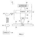
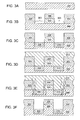
- An absorber layer 312 is deposited according to embodiments of the present invention on the substrate 300, as shown in Figure 3D .
- the absorber layer 312 is configured to provide a uniform thermal absorption coefficient across the substrate 300 despite the difference among the field oxide layer 302, the gate electrode 306, the gate source 308 and the gate drain 310.
- the absorber layer 312 comprises carbon.
- the carbon in the absorber layer 312 increases the overall light absorption coefficient.
- the absorber layer 312 comprises graphitized carbon black. Properties of the high temperature carbon in the absorber layer 312 remain stable during the annealing process to be followed.
- the substrate 300 is kept within a low temperature, such as under about 450°C, while depositing the absorber layer 312.
- Various methods such as spin-on, sooty flame, physical vapor deposition, electrophoretic deposition and electrostatic deposition, may be used to deposit the absorber layer 312. Detailed description of these methods is to follow.
- Figures 3A-3F show only one gate device on a substrate, it is recognized that the layers described herein will typically be formed on a substrate that includes a plurality of devices of different sizes, types, and materials and spaced at varying densities across the surface of the substrate. It is believed that the layers promote uniform heating across a surface of the substrate during annealing of the substrate in spite of varying device topography across the surface of a substrate.
- a colloidal solution of materials for the absorber layer such as graphitized carbon black, fullerene, or modified fullerene, may be formed and dispensed on a spinning substrate to form a coat of the colloidal solution.
- the absorber layer may be formed by curing the colloidal solution at a temperature lower than the annealing temperature.
Landscapes
- Formation Of Insulating Films (AREA)
- Physical Vapour Deposition (AREA)
- Chemical Vapour Deposition (AREA)
- Manufacturing Of Magnetic Record Carriers (AREA)
- Braking Arrangements (AREA)
- Carbon And Carbon Compounds (AREA)
- Container, Conveyance, Adherence, Positioning, Of Wafer (AREA)
Applications Claiming Priority (1)
| Application Number | Priority Date | Filing Date | Title |
|---|---|---|---|
| US11/681,343 US7867868B2 (en) | 2007-03-02 | 2007-03-02 | Absorber layer candidates and techniques for application |
Publications (3)
| Publication Number | Publication Date |
|---|---|
| EP1965419A2 EP1965419A2 (en) | 2008-09-03 |
| EP1965419A3 EP1965419A3 (en) | 2011-03-23 |
| EP1965419B1 true EP1965419B1 (en) | 2013-07-03 |
Family
ID=39413092
Family Applications (1)
| Application Number | Title | Priority Date | Filing Date |
|---|---|---|---|
| EP08152073.6A Active EP1965419B1 (en) | 2007-03-02 | 2008-02-28 | Absorber layer candidates and techniques for application |
Country Status (6)
| Country | Link |
|---|---|
| US (1) | US7867868B2 (enExample) |
| EP (1) | EP1965419B1 (enExample) |
| JP (1) | JP5422132B2 (enExample) |
| KR (1) | KR100931766B1 (enExample) |
| CN (1) | CN101256938A (enExample) |
| TW (1) | TWI430370B (enExample) |
Families Citing this family (14)
| Publication number | Priority date | Publication date | Assignee | Title |
|---|---|---|---|---|
| US7772064B2 (en) * | 2007-03-05 | 2010-08-10 | United Microelectronics Corp. | Method of fabricating self-aligned contact |
| US7947584B2 (en) * | 2008-05-02 | 2011-05-24 | Applied Materials, Inc. | Suitably short wavelength light for laser annealing of silicon in DSA type systems |
| US20120015459A1 (en) * | 2010-07-15 | 2012-01-19 | Taiwan Semiconductor Manufacturing Company, Ltd. | Thermal Leveling for Semiconductor Devices |
| US8603575B1 (en) * | 2010-10-06 | 2013-12-10 | Nanosolar, Inc. | Thin-film absorber formation method |
| CN102637581A (zh) * | 2012-04-06 | 2012-08-15 | 上海华力微电子有限公司 | 一种防止硼掺杂层释气的方法 |
| GB201211786D0 (en) * | 2012-07-03 | 2012-08-15 | Cambridge Display Tech Ltd | Organic electronic device manufacturing techniques |
| US9029809B2 (en) * | 2012-11-30 | 2015-05-12 | Ultratech, Inc. | Movable microchamber system with gas curtain |
| CN103489763A (zh) * | 2013-09-29 | 2014-01-01 | 武汉新芯集成电路制造有限公司 | 一种避免离子注入掺杂离子释气的方法 |
| JP5770880B2 (ja) * | 2014-04-08 | 2015-08-26 | 株式会社Screenホールディングス | 熱処理方法 |
| CN105047560A (zh) * | 2015-07-01 | 2015-11-11 | 复旦大学 | 微波退火工艺 |
| CN105977153B (zh) * | 2016-05-17 | 2019-09-17 | 上海华力微电子有限公司 | 超浅结退火方法 |
| CN106099079A (zh) * | 2016-08-26 | 2016-11-09 | 宁德时代新能源科技股份有限公司 | 二次电池负极材料,其制备方法及含有该负极材料的电池 |
| CN107564801A (zh) * | 2017-08-31 | 2018-01-09 | 长江存储科技有限责任公司 | 一种退火方法 |
| CN110364434A (zh) * | 2019-07-19 | 2019-10-22 | 德淮半导体有限公司 | 退火方法和半导体器件的制造方法 |
Citations (2)
| Publication number | Priority date | Publication date | Assignee | Title |
|---|---|---|---|---|
| US20040241934A1 (en) * | 2003-04-10 | 2004-12-02 | Seiko Epson Corporation | Method of manufacturing semiconductor device, integrated circuit, electro-optical device, and electronic apparatus |
| US20060263540A1 (en) * | 2005-05-17 | 2006-11-23 | Kartik Ramaswamy | Process for low temperature plasma deposition of an optical absorption layer and high speed optical annealing |
Family Cites Families (19)
| Publication number | Priority date | Publication date | Assignee | Title |
|---|---|---|---|---|
| US2688576A (en) * | 1949-12-21 | 1954-09-07 | St Regis Paper Co | Electrically conductive resinous laminate |
| US3421967A (en) * | 1965-03-03 | 1969-01-14 | Kaumagraph Co | Decorated thermosetting plastic article and method of producing same |
| US3520656A (en) * | 1966-03-30 | 1970-07-14 | Du Pont | Silicon carbide compositions |
| US4025661A (en) * | 1972-11-13 | 1977-05-24 | Rca Corporation | Method of making viewing-screen structure for a cathode-ray tube |
| US4664768A (en) * | 1985-03-28 | 1987-05-12 | Westinghouse Electric Corp. | Reinforced composites made by electro-phoretically coating graphite or carbon |
| US5308481A (en) * | 1992-06-02 | 1994-05-03 | Analytical Bio-Chemistry Laboratories, Inc. | Chemically bound fullerenes to resin and silica supports and their use as stationary phases for chromatography |
| US5461123A (en) * | 1994-07-14 | 1995-10-24 | Union Carbide Chemicals & Plastics Technology Corporation | Gas phase fluidized bed polyolefin polymerization process using sound waves |
| US6276072B1 (en) | 1997-07-10 | 2001-08-21 | Applied Materials, Inc. | Method and apparatus for heating and cooling substrates |
| US6302960B1 (en) | 1998-11-23 | 2001-10-16 | Applied Materials, Inc. | Photoresist coater |
| US6627056B2 (en) | 2000-02-16 | 2003-09-30 | Applied Materials, Inc. | Method and apparatus for ionized plasma deposition |
| US6573030B1 (en) | 2000-02-17 | 2003-06-03 | Applied Materials, Inc. | Method for depositing an amorphous carbon layer |
| KR100365414B1 (en) * | 2001-04-30 | 2002-12-18 | Hynix Semiconductor Inc | Method for forming ultra-shallow junction using laser annealing process |
| US6660449B2 (en) * | 2001-10-19 | 2003-12-09 | Eastman Kodak Company | Heat-sensitive compositions and imaging member containing carbon black and methods of imaging and printing |
| JP2005072205A (ja) * | 2003-08-22 | 2005-03-17 | Seiko Epson Corp | 熱処理方法、配線パターンの形成方法、電気光学装置の製造方法、電気光学装置及び電子機器 |
| WO2005036627A1 (en) | 2003-10-03 | 2005-04-21 | Applied Materials, Inc. | Absorber layer for dynamic surface annealing processing |
| US7109087B2 (en) | 2003-10-03 | 2006-09-19 | Applied Materials, Inc. | Absorber layer for DSA processing |
| US7323401B2 (en) | 2005-08-08 | 2008-01-29 | Applied Materials, Inc. | Semiconductor substrate process using a low temperature deposited carbon-containing hard mask |
| JP5057261B2 (ja) * | 2005-10-25 | 2012-10-24 | 東海カーボン株式会社 | カーボンブラック水性分散体及びその製造方法 |
| US20090026704A1 (en) * | 2007-07-24 | 2009-01-29 | Werner Alecsander Kling | 123 poker |
-
2007
- 2007-03-02 US US11/681,343 patent/US7867868B2/en active Active
-
2008
- 2008-02-28 EP EP08152073.6A patent/EP1965419B1/en active Active
- 2008-02-29 TW TW097107143A patent/TWI430370B/zh active
- 2008-02-29 CN CNA2008100063787A patent/CN101256938A/zh active Pending
- 2008-02-29 KR KR1020080018836A patent/KR100931766B1/ko active Active
- 2008-03-03 JP JP2008052417A patent/JP5422132B2/ja active Active
Patent Citations (2)
| Publication number | Priority date | Publication date | Assignee | Title |
|---|---|---|---|---|
| US20040241934A1 (en) * | 2003-04-10 | 2004-12-02 | Seiko Epson Corporation | Method of manufacturing semiconductor device, integrated circuit, electro-optical device, and electronic apparatus |
| US20060263540A1 (en) * | 2005-05-17 | 2006-11-23 | Kartik Ramaswamy | Process for low temperature plasma deposition of an optical absorption layer and high speed optical annealing |
Also Published As
| Publication number | Publication date |
|---|---|
| KR100931766B1 (ko) | 2009-12-14 |
| TW200845225A (en) | 2008-11-16 |
| US20080214014A1 (en) | 2008-09-04 |
| US7867868B2 (en) | 2011-01-11 |
| JP5422132B2 (ja) | 2014-02-19 |
| JP2008270746A (ja) | 2008-11-06 |
| EP1965419A3 (en) | 2011-03-23 |
| KR20080080936A (ko) | 2008-09-05 |
| TWI430370B (zh) | 2014-03-11 |
| EP1965419A2 (en) | 2008-09-03 |
| CN101256938A (zh) | 2008-09-03 |
Similar Documents
| Publication | Publication Date | Title |
|---|---|---|
| EP1965419B1 (en) | Absorber layer candidates and techniques for application | |
| CN100459050C (zh) | 用于动态表面退火工艺的吸收层 | |
| KR20190135003A (ko) | 반도체 소자를 제조하기 위한 장치 및 방법 | |
| KR100639071B1 (ko) | 박막 작성 시스템 | |
| KR102616691B1 (ko) | 챔버 부품들을 제조하기 위한 방법 | |
| JP4884268B2 (ja) | アッシング方法 | |
| KR20200096985A (ko) | 셔터 디스크 어셈블리, 반도체 가공 장치와 방법 | |
| US11756819B2 (en) | Methods and apparatus for minimizing substrate backside damage | |
| EP1676300B1 (en) | Method for annealing a substrate comprising an absorber layer | |
| WO2023039382A1 (en) | Atomic layer etching using boron trichloride | |
| JP7835587B2 (ja) | 基板乾燥方法と基板処理方法 |
Legal Events
| Date | Code | Title | Description |
|---|---|---|---|
| PUAI | Public reference made under article 153(3) epc to a published international application that has entered the european phase |
Free format text: ORIGINAL CODE: 0009012 |
|
| AK | Designated contracting states |
Kind code of ref document: A2 Designated state(s): AT BE BG CH CY CZ DE DK EE ES FI FR GB GR HR HU IE IS IT LI LT LU LV MC MT NL NO PL PT RO SE SI SK TR |
|
| AX | Request for extension of the european patent |
Extension state: AL BA MK RS |
|
| PUAL | Search report despatched |
Free format text: ORIGINAL CODE: 0009013 |
|
| AK | Designated contracting states |
Kind code of ref document: A3 Designated state(s): AT BE BG CH CY CZ DE DK EE ES FI FR GB GR HR HU IE IS IT LI LT LU LV MC MT NL NO PL PT RO SE SI SK TR |
|
| AX | Request for extension of the european patent |
Extension state: AL BA MK RS |
|
| 17P | Request for examination filed |
Effective date: 20110920 |
|
| AKX | Designation fees paid |
Designated state(s): DE FR |
|
| 17Q | First examination report despatched |
Effective date: 20120606 |
|
| GRAP | Despatch of communication of intention to grant a patent |
Free format text: ORIGINAL CODE: EPIDOSNIGR1 |
|
| GRAS | Grant fee paid |
Free format text: ORIGINAL CODE: EPIDOSNIGR3 |
|
| GRAA | (expected) grant |
Free format text: ORIGINAL CODE: 0009210 |
|
| AK | Designated contracting states |
Kind code of ref document: B1 Designated state(s): DE FR |
|
| REG | Reference to a national code |
Ref country code: DE Ref legal event code: R096 Ref document number: 602008025678 Country of ref document: DE Effective date: 20130829 |
|
| PLBE | No opposition filed within time limit |
Free format text: ORIGINAL CODE: 0009261 |
|
| STAA | Information on the status of an ep patent application or granted ep patent |
Free format text: STATUS: NO OPPOSITION FILED WITHIN TIME LIMIT |
|
| 26N | No opposition filed |
Effective date: 20140404 |
|
| REG | Reference to a national code |
Ref country code: DE Ref legal event code: R097 Ref document number: 602008025678 Country of ref document: DE Effective date: 20140404 |
|
| REG | Reference to a national code |
Ref country code: FR Ref legal event code: PLFP Year of fee payment: 9 |
|
| REG | Reference to a national code |
Ref country code: FR Ref legal event code: PLFP Year of fee payment: 10 |
|
| REG | Reference to a national code |
Ref country code: FR Ref legal event code: PLFP Year of fee payment: 11 |
|
| REG | Reference to a national code |
Ref country code: DE Ref legal event code: R079 Ref document number: 602008025678 Country of ref document: DE Free format text: PREVIOUS MAIN CLASS: H01L0021324000 Ipc: H10P0095900000 |
|
| PGFP | Annual fee paid to national office [announced via postgrant information from national office to epo] |
Ref country code: FR Payment date: 20251015 Year of fee payment: 19 |
|
| PGFP | Annual fee paid to national office [announced via postgrant information from national office to epo] |
Ref country code: DE Payment date: 20251015 Year of fee payment: 19 |