EP1962335A1 - Method of processing chamfered portion of semiconductor wafer and method of correcting groove shape of grindstone - Google Patents
Method of processing chamfered portion of semiconductor wafer and method of correcting groove shape of grindstone Download PDFInfo
- Publication number
- EP1962335A1 EP1962335A1 EP06834569A EP06834569A EP1962335A1 EP 1962335 A1 EP1962335 A1 EP 1962335A1 EP 06834569 A EP06834569 A EP 06834569A EP 06834569 A EP06834569 A EP 06834569A EP 1962335 A1 EP1962335 A1 EP 1962335A1
- Authority
- EP
- European Patent Office
- Prior art keywords
- grinding
- grinding stone
- chamfer portion
- groove
- truer
- Prior art date
- Legal status (The legal status is an assumption and is not a legal conclusion. Google has not performed a legal analysis and makes no representation as to the accuracy of the status listed.)
- Granted
Links
- 239000004065 semiconductor Substances 0.000 title claims abstract description 41
- 238000000034 method Methods 0.000 title claims abstract description 32
- 239000004575 stone Substances 0.000 claims abstract description 213
- 239000011347 resin Substances 0.000 claims abstract description 92
- 229920005989 resin Polymers 0.000 claims abstract description 92
- 238000003754 machining Methods 0.000 claims abstract description 22
- ZZUFCTLCJUWOSV-UHFFFAOYSA-N furosemide Chemical compound C1=C(Cl)C(S(=O)(=O)N)=CC(C(O)=O)=C1NCC1=CC=CO1 ZZUFCTLCJUWOSV-UHFFFAOYSA-N 0.000 claims abstract description 11
- 239000002184 metal Substances 0.000 claims description 34
- 229910052751 metal Inorganic materials 0.000 claims description 34
- 229910052710 silicon Inorganic materials 0.000 claims description 34
- 239000010703 silicon Substances 0.000 claims description 34
- XUIMIQQOPSSXEZ-UHFFFAOYSA-N Silicon Chemical compound [Si] XUIMIQQOPSSXEZ-UHFFFAOYSA-N 0.000 claims description 33
- 239000006061 abrasive grain Substances 0.000 claims description 10
- 239000000463 material Substances 0.000 claims description 8
- 239000005011 phenolic resin Substances 0.000 claims description 8
- HBMJWWWQQXIZIP-UHFFFAOYSA-N silicon carbide Chemical compound [Si+]#[C-] HBMJWWWQQXIZIP-UHFFFAOYSA-N 0.000 claims description 6
- 229910010271 silicon carbide Inorganic materials 0.000 claims description 6
- 235000012431 wafers Nutrition 0.000 description 110
- 230000000052 comparative effect Effects 0.000 description 8
- 229910003460 diamond Inorganic materials 0.000 description 4
- 239000010432 diamond Substances 0.000 description 4
- 238000004519 manufacturing process Methods 0.000 description 3
- 238000005498 polishing Methods 0.000 description 3
- 238000001179 sorption measurement Methods 0.000 description 3
- 230000015572 biosynthetic process Effects 0.000 description 2
- 239000013078 crystal Substances 0.000 description 2
- 239000000945 filler Substances 0.000 description 2
- 238000005259 measurement Methods 0.000 description 2
- 239000002245 particle Substances 0.000 description 2
- 239000000843 powder Substances 0.000 description 2
- 230000002035 prolonged effect Effects 0.000 description 2
- 229910052582 BN Inorganic materials 0.000 description 1
- PZNSFCLAULLKQX-UHFFFAOYSA-N Boron nitride Chemical compound N#B PZNSFCLAULLKQX-UHFFFAOYSA-N 0.000 description 1
- 238000005299 abrasion Methods 0.000 description 1
- 238000010521 absorption reaction Methods 0.000 description 1
- 239000011230 binding agent Substances 0.000 description 1
- 239000006229 carbon black Substances 0.000 description 1
- 239000000470 constituent Substances 0.000 description 1
- 238000007796 conventional method Methods 0.000 description 1
- 229910052802 copper Inorganic materials 0.000 description 1
- 238000012937 correction Methods 0.000 description 1
- 230000000694 effects Effects 0.000 description 1
- 239000003822 epoxy resin Substances 0.000 description 1
- 229920000647 polyepoxide Polymers 0.000 description 1
- 229920013716 polyethylene resin Polymers 0.000 description 1
- 229920001721 polyimide Polymers 0.000 description 1
- 239000009719 polyimide resin Substances 0.000 description 1
- 229920005990 polystyrene resin Polymers 0.000 description 1
- 238000011160 research Methods 0.000 description 1
- 150000003376 silicon Chemical class 0.000 description 1
- 230000003746 surface roughness Effects 0.000 description 1
Images


Classifications
-
- H—ELECTRICITY
- H01—ELECTRIC ELEMENTS
- H01L—SEMICONDUCTOR DEVICES NOT COVERED BY CLASS H10
- H01L21/00—Processes or apparatus adapted for the manufacture or treatment of semiconductor or solid state devices or of parts thereof
- H01L21/02—Manufacture or treatment of semiconductor devices or of parts thereof
- H01L21/02002—Preparing wafers
- H01L21/02005—Preparing bulk and homogeneous wafers
- H01L21/02008—Multistep processes
- H01L21/0201—Specific process step
- H01L21/02021—Edge treatment, chamfering
-
- H—ELECTRICITY
- H01—ELECTRIC ELEMENTS
- H01L—SEMICONDUCTOR DEVICES NOT COVERED BY CLASS H10
- H01L21/00—Processes or apparatus adapted for the manufacture or treatment of semiconductor or solid state devices or of parts thereof
- H01L21/02—Manufacture or treatment of semiconductor devices or of parts thereof
- H01L21/04—Manufacture or treatment of semiconductor devices or of parts thereof the devices having at least one potential-jump barrier or surface barrier, e.g. PN junction, depletion layer or carrier concentration layer
- H01L21/18—Manufacture or treatment of semiconductor devices or of parts thereof the devices having at least one potential-jump barrier or surface barrier, e.g. PN junction, depletion layer or carrier concentration layer the devices having semiconductor bodies comprising elements of Group IV of the Periodic System or AIIIBV compounds with or without impurities, e.g. doping materials
- H01L21/30—Treatment of semiconductor bodies using processes or apparatus not provided for in groups H01L21/20 - H01L21/26
- H01L21/302—Treatment of semiconductor bodies using processes or apparatus not provided for in groups H01L21/20 - H01L21/26 to change their surface-physical characteristics or shape, e.g. etching, polishing, cutting
- H01L21/304—Mechanical treatment, e.g. grinding, polishing, cutting
-
- B—PERFORMING OPERATIONS; TRANSPORTING
- B24—GRINDING; POLISHING
- B24B—MACHINES, DEVICES, OR PROCESSES FOR GRINDING OR POLISHING; DRESSING OR CONDITIONING OF ABRADING SURFACES; FEEDING OF GRINDING, POLISHING, OR LAPPING AGENTS
- B24B53/00—Devices or means for dressing or conditioning abrasive surfaces
- B24B53/06—Devices or means for dressing or conditioning abrasive surfaces of profiled abrasive wheels
- B24B53/07—Devices or means for dressing or conditioning abrasive surfaces of profiled abrasive wheels by means of forming tools having a shape complementary to that to be produced, e.g. blocks, profile rolls
-
- B—PERFORMING OPERATIONS; TRANSPORTING
- B24—GRINDING; POLISHING
- B24B—MACHINES, DEVICES, OR PROCESSES FOR GRINDING OR POLISHING; DRESSING OR CONDITIONING OF ABRADING SURFACES; FEEDING OF GRINDING, POLISHING, OR LAPPING AGENTS
- B24B9/00—Machines or devices designed for grinding edges or bevels on work or for removing burrs; Accessories therefor
- B24B9/02—Machines or devices designed for grinding edges or bevels on work or for removing burrs; Accessories therefor characterised by a special design with respect to properties of materials specific to articles to be ground
- B24B9/06—Machines or devices designed for grinding edges or bevels on work or for removing burrs; Accessories therefor characterised by a special design with respect to properties of materials specific to articles to be ground of non-metallic inorganic material, e.g. stone, ceramics, porcelain
- B24B9/065—Machines or devices designed for grinding edges or bevels on work or for removing burrs; Accessories therefor characterised by a special design with respect to properties of materials specific to articles to be ground of non-metallic inorganic material, e.g. stone, ceramics, porcelain of thin, brittle parts, e.g. semiconductors, wafers
Definitions
- the present invention relates to a method for precisely grinding a chamfer portion of a semiconductor wafer, e.g., a silicon wafer, based on helical grinding.
- a semiconductor wafer e.g., a silicon wafer, for use in fabrication of a semiconductor device and the like is chamfered by grinding an edge portion in order to avoid chipping due to handling, and also subjected to mirror edge polishing based on polishing as a particle generation countermeasure in a device process in recent years.
- a mechanical damage in the chamfer portion is deep, a damage or a grinding striation remains even though mirror edge polishing is performed, which results in a factor of particle generation.
- a method for reducing a mechanical damage in the chamfer portion there is a method for performing so-called helical grinding with respect to a chamfer portion of a wafer, for example, while inclining a resin bond grinding stone (a resin grinding stone) with respect to the wafer (see Japanese Patent Application publication No. H05-152259 ).
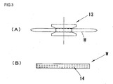
- a chamfer portion is ground in a state where a main surface of a wafer W becomes vertical to a rotating axis of a resin grinding stone 13 as shown in FIG. 3(A) , but in this case, grinding striations 14 in a circumferential direction are apt to be generated in the chamfer portion as shown in FIG. 3(B) .
- the chamfer portion of the wafer W is ground in a state where the rotating axis of the resin grinding stone 13 is inclined with respect to a rotating axis of the wafer W as shown in FIG. 4(A) .
- the chamfer portion of the wafer W contacts with the surface of the grinding stone 13, thus an effect of improving surface roughness of the chamfer portion as compared with regular grinding is obtained.
- a main object of the present invention is to provide a method for machining a chamfer portion of a semiconductor wafer, which can chamfer the chamfer portion of the wafer into a vertically symmetrical shape when subjecting the chamber portion of the semiconductor wafer to helical grinding by using, e.g., a resin grinding stone.
- a method for machining a chamfer portion of a semiconductor wafer that is a method for subjecting a roughly ground chamfer portion of a semiconductor wafer to helical grinding by relatively inclining the wafer and a second grinding stone to perform precise grinding, comprising: forming an edge portion of a discoid truer into a vertically asymmetrical groove shape of a first grinding stone by using the first grinding stone having a vertically asymmetrical groove formed on a periphery thereof to grind the edge portion of the truer without being relatively inclined; forming a groove on a periphery of the second grinding stone by relatively inclining the truer and the second grinding stone to subject the second grinding stone to helical grinding; and precisely grinding the chamfer portion of the wafer based on helical grinding by relatively inclining the semiconductor wafer with respect to a direction of the groove formed on the periphery of the second grinding stone.
- the substantially vertically symmetrical groove can be formed on the periphery of the second grinding stone. Furthermore, if the second grinding stone is used to subject the chamfer portion of the wafer to helical grinding, the chamfer portion of the wafer can be machined into the substantially vertically symmetrical shape.
- a metal grinding stone can be used as the first grinding stone, and a resin grinding stone can be used as the second grinding stone.
- the resin grinding stone is preferable for precise grinding for the chamfer portion of the semiconductor wafer.
- the metal grinding stone is harder than the resin grinding stone and preferable for machining of the truer.
- upper and lower angles of the groove of the first grinding stone are determined in such a manner that the vertically asymmetrical shape of the edge portion of the truer can be offset and a vertically symmetrical groove can be formed on the periphery of the second grinding stone. If the upper and lower angles of the groove of the first grinding stone are determined to subject the second grinding stone to helical grinding through the truer, the groove having the substantially vertically symmetrical shape can be more certainly formed.
- a material formed by combining abrasive grains consisting of a silicon carbide through a phenol resin can be used.
- the truer formed by combining abrasive grains consisting of the silicon carbide through the phenol resin can be preferably machined by using the first grinding stone a metal grinding stone and the like.
- the second grinding stone e.g., a resin grinding stone and the like can be preferably machined by using the machined truer.
- the silicon wafer is most frequently used for fabrication of a semiconductor device and the like, and the present invention is very useful for machining the chamfer portion of the silicon wafer.
- a target value of the upper and lower angles of the chamfer portion of the semiconductor wafer after precise grinding based on helical grinding using the second grinding stone can be set to 22 degrees.
- each of the upper and lower angles of the chamfer portion becomes very close to 22 degrees as a general target, thereby obtaining the chamfer portion having the substantially vertical symmetrical shape can be machined.
- the second grinding stone having the substantially vertically symmetrical groove formed thereon can be used to subject the wafer to helical grinding, but in this case, the groove shape of the second grinding stone gradually varies due to continuous machining.
- the chamfer portion is subjected to rough grinding in advance in such a manner that the side of the chamfer portion of the wafer that is apt to have a large angle after helical grinding has a small angle, the chamfer portion can be certainly machined into one having the substantially vertically symmetrical shape after helical grinding.
- a method for correcting a groove shape of a second grinding stone that is a method for correcting a groove shape of a second grinding stone when a semiconductor wafer having a roughly ground chamfer portion and the second grinding stone having a groove formed on a periphery thereof are relatively inclined and the chamfer portion of the wafer is subjected to helical grinding using the groove of the second grinding stone to perform precise grinding, comprising: forming an edge portion of a discoid truer into a vertically asymmetrical groove shape of a first grinding stone by using the first grinding stone having a vertically asymmetrical groove formed on a periphery thereof to grind the edge portion of the truer; and correcting the groove shape of the second grinding stone by relatively inclining the truer and the second grinding stone to subject the second grinding stone to helical grinding.
- the groove of the second grinding stone for grinding is worn out or clogged, and hence the groove shape gradually varies.
- the first grinding stone having the vertically asymmetrical groove formed on the periphery thereof is used to form the edge portion of the truer and the groove shape of the second grinding stone is corrected through the truer based on helical grinding, the groove of the second grinding stone can be reproduced into the substantially vertically symmetrical shape.
- the first grinding stone e.g., a metal grinding stone having a vertically asymmetrical groove formed on a periphery thereof is used to machine the truer
- the substantially vertically symmetrical groove is formed or corrected on the periphery of the second grinding stone, e.g., a resin grinding stone based on helical grinding using the truer.
- the second grinding stone is used to subject the chamfer portion of the wafer to helical grinding, the chamfer portion of the wafer can be machined into a substantially vertically symmetrical shape.
- the present inventor has examined a cause that shape of a chamfer portion of a wafer becomes vertically asymmetrical when the chamber portion of the silicon wafer is subjected to helical grinding by using a resin grinding stone (a second grinding stone).
- a resin grinding stone a second grinding stone.
- machining a chamfer portion of a silicon wafer in such a manner that each of upper and lower angles of the chamfer portion of the silicon wafer becomes 22 degrees a metal grinding stone 21 having a vertically symmetrical groove 24 in which each of upper and lower angles is 22 degrees is first fabricated as a prototype (a first grinding stone) as shown in FIG. 5(A) .
- a discoid truer 22 is horizontally pressed against the vertically symmetrical groove 24 of the metal grinding stone 21 to grind an edge portion of the truer 22 ( FIG. 5 (B) ).
- the edge portion of the truer 22 is formed into a vertically symmetrical shape at an angle equal to that of the groove shape of the metal grinding stone 21, that is, 22 degrees.
- a resin grinding stone 23 having no grinding groove formed thereon is obliquely attached to a helical chamfering machine, and a truer 22a having a formed edge portion is held on an absorption table 26 to perform helical grinding. That is, when the groove shape of the metal grinding stone 21 is transferred to the resin grinding stone 23 through the truer 22a in the helical chamfering machine, a groove required to grind the chamfer portion of the wafer can be formed on a periphery of the resin grinding stone 23.
- the present inventor has also keenly studied a method for machining a shape of a chamfer portion into a vertically symmetrical shape even when subjecting the chamber portion of the semiconductor wafer to helical grinding.
- a metal grinding stone having a vertically asymmetrical groove is used as a prototype to machine an edge portion of a truer and the vertically asymmetrical truer is used to subject a resin grinding stone to helical grinding
- a groove having a substantially vertically symmetrical shape can be formed on a periphery of the resin grinding stone, and that if the chamfer portion of the semiconductor wafer is machined based on helical grinding by using the resin grinding stone, the chamfer portion of the wafer can be machined into a substantially vertically symmetrical shape, thereby bringing the present invention to completion.
- FIG. 1 is a flowchart showing an example of a process of machining a chamfer portion of a silicon wafer according to the present invention
- FIG. 2 is explanatory drawings showing a procedure for forming a groove on a resin grinding stone.
- a metal grinding stone 1 having a vertically asymmetrical groove 4 formed thereon is prepared as a prototype (a first grinding stone) ( FIG. 1(A) , FIG. 2(A) ).
- a metal grinding stone 1 one formed by mixing diamond abrasive grains in a main component, e.g., a metal powder of Fe, Cr, or Cu and the like, can be preferably used.
- the asymmetrical groove shape of the metal grinding stone 1 is reflected in a shape of an edge portion of a truer formed by grinding using the groove 4, and affects a shape of a groove formed by using the truer to subject the resin grinding stone (a second grinding stone) to helical grinding. Therefore, each of upper and lower angles ⁇ 1 and ⁇ 2 of the groove 4 of the metal grinding stone may be determined while considering a groove shape of the resin grinding stone and the like.
- the upper and lower angles ⁇ 1 and ⁇ 2 of the groove 4 of the metal grinding stone 1 in such a manner that a vertically asymmetrical shape of the edge portion of the truer is offset to enable formation of the vertically symmetrical groove on the periphery of the resin grinding stone when the resin grinding stone is ground (helical grinding) while relatively inclining the truer and the resin grinding stone.
- the edge portion of the discoid truer 2 is ground by using the vertically asymmetrical groove 4 of the metal grinding stone 1 without being relatively inclined, thereby forming the vertical asymmetrical shape of the metal grinding stone 1 ( FIG. 1(B) , FIG. 2 (B) ).
- a material of the truer 2 one that can be machined by the metal grinding stone 1 and can grind the resin grinding stone is adopted.
- a material obtained by combining abrasive grains consisting of a silicon carbide through a phenol resin added a filler and the like therein if necessary and forming a resultant into a discoid truer can be preferably used.
- the truer formed from the silicon carbide and the phenol resin can be preferably machined by using the metal grinding stone and, when forming or correcting the groove of the resin grinding stone, abrasion of the truer can be suppressed, and the same truer can be utilized to repeatedly subject the groove of the resin grinding stone to truing.
- a truer 2a having an edge portion machined into a vertically asymmetrical shape is used to form a groove 5 on a periphery of a resin grinding stone 3 ( FIG. 2(C) and (D) ).
- the resin grinding stone 3 is ground while relatively inclining the truer 2a and the resin grinding stone 3 in a tangential direction at a predetermined angle, thereby forming the groove 5 on the periphery of the resin grinding stone 3 ( FIG. 1(C) ).
- a material of the resin grinding stone 3 one that can form the groove 5 on the periphery when ground by the truer and can precisely grind a chamfer portion of a silicon wafer by the formed groove 5 is adopted.
- a material that contains a phenol resin, an epoxy resin, a polyimide resin and the like, a polystyrene resin, or a polyethylene resin as a main component and is formed by mixing diamond abrasive grains or cubic crystal boron nitride abrasive grains in this main component can be preferably used.
- the resin grinding stone 3 When forming the groove 5 on the resin grinding stone 3, the resin grinding stone 3 is attached to a helical chamfering machine (not shown) at a predetermined inclination angle, and the truer 2a having the edge portion formed thereon is held on an adsorption table 6 of the helical chamfering machine to perform helical grinding.
- a helical chamfering machine not shown
- the truer 2a having the edge portion formed thereon is held on an adsorption table 6 of the helical chamfering machine to perform helical grinding.
- the vertical asymmetrical shape of the edge portion of the truer 2a is offset, thereby forming the groove 5 having a substantially vertically symmetrical shape on the periphery of the resin grinding stone 3a ( FIG. 2(E) ).
- the silicon wafer is relatively inclined with respect to a direction of the groove formed on the periphery of the resin grinding stone 3a through the above described process to precisely grind the chamfer portion of the wafer based on helical grinding ( FIG. 1 (D) ). It is to be noted that the silicon wafer is subjected to rough chamfering by roughly grinding an edge portion thereof by using the metal grinding stone in advance. If the chamfer portion of the wafer is roughly ground in advance, the chamfer portion can be precisely ground in a short time based on helical grinding using the resin grinding stone 3a, and a life of the resin grinding stone can be prolonged.
- the groove shape of the resin grinding stone 3a is reflected in the chamfer portion of the wafer, thereby machining the chamfer portion into one having the substantially vertically symmetrical shape.
- the resin grinding stone 3a when continuous machining is carried out, the resin grinding stone 3a is worn out or clogged to change its groove shape, and vertical symmetry of the groove gradually collapses.
- the vertical symmetry of the groove shape of the resin grinding stone 3a is degraded, appropriately performing helical grinding as well as the above described case of forming the groove 5 using the truer 2a, the groove shape can be corrected (truing) into one having the high vertical symmetry.
- rough grinding may be carried out before precisely grinding the chamfer portion of the silicon wafer based on helical grinding using the resin grinding stone 3a so that the chamfer portion of the wafer can have a slightly vertically asymmetrical shape.
- the chamfer portion of the wafer is continuously machined based on helical grinding, for example, if the upper angle of the chamfer portion tends to become large, rough grinding is performed so that the upper angle of the chamfer portion of the wafer becomes small.
- the chamfer portion of the wafer can be continuously machined to have the substantially vertically symmetrical shape.
- the metal grinding stone (the prototype, the first grinding stone) having the vertically symmetrical groove is used to form the substantially vertically symmetrical groove to the resin grinding stone (the second grinding stone) through the truer and the chamfer portion of the roughly ground wafer is subjected to helical grinding, thereby the chamfer portion can be machined to have the substantially vertically symmetrical shape.
- the groove of the resin grinding stone is subjected to truing according to the present invention the number of wafers that can be machined per a truing operation can be increased and also a life of the resin grinding stone can be prolonged, thereby increasing the number of wafers that can be machined by using the single resin grinding stone. Therefore, a cost in manufacture of the semiconductor wafer can be reduced.
- a metal grinding stone (main components: a metal powder (Fe, Cr, Cu), diamond abrasive grains) having a vertically asymmetrical groove with an upper angle of 22 degrees and a lower angle of 21 degrees formed on a periphery thereof was prepared as a prototype.
- An edge portion of a discoid truer was ground to be formed into a groove shape of the metal grinding stone by the groove of the metal grinding stone without being relatively inclined.
- a configuration of the truer is as shown in the following Table 1.
- the truer having the edge portion formed as explained above was held on an adsorption table of a helical chamfering machine, and a periphery of an obliquely attached resin grinding stone (main components: a phenol resin, diamond abrasive grains) was subjected to helical grinding, thereby forming a groove on the periphery of the resin grinding stone.
- main components a phenol resin, diamond abrasive grains
- a metal grinding stone having a vertical symmetrical groove with both upper and lower angles of 22 degrees was prepared as a prototype.
- An edge portion of a discoid truer was ground to be formed into a groove shape of the metal grinding stone by the groove of the metal grinding stone, and a periphery of a resin grinding stone was subjected to helical grinding by using the truer to form a groove. It is to be noted that configurations of materials of the metal grinding stone, the truer, and the resin grinding stone are the same as those of Example 1.
- An edge portion of a silicon wafer obtained by slicing a silicon single crystal ingot grown based on a Czochralski method was subjected to rough chamfering.
- This silicon wafer was held on an adsorption table of a helical chamfering machine including the resin grinding stone according to Example 1, and a chamfer portion of the wafer was precisely ground by the groove formed on the periphery of the resin grinding stone based on helical grinding.
- FIG. 6(A) shows a number of each machined wafer and upper and lower angles of the chamfer portion of each wafer after precise grinding using the resin grinding stone. Both the upper and lower angles of the chamfer portion of each wafer were close to a target value (22 degrees) to form a substantially symmetrical shape, and the margin of error of both the upper and lower angles were within ⁇ 1 degree.
- FIG. 6(B) shows a measurement result of a width of a front end of each chamfer portion, and the respective widths slightly fluctuate near a target value (320 ⁇ m), but they were averagely very close to the target value.
- FIG. 7(A) shows a number of each machined wafer and upper and lower angles of the chamfer portion of each wafer after precise grinding using the resin grinding stone. Both the upper and lower angles of the chamfer portion greatly deviate from the target value (22 degrees), most of the lower angles exceed 23 degrees, and it can be understood that each chamfer portion was formed into a vertically asymmetrical shape. Moreover, as shown in FIG.7(B) , front ends of the most chamfer portions of about the 20th and subsequent wafers had widths that are approximately 10 ⁇ m smaller than the target value (320 ⁇ m.
- a chamfer portion of each silicon wafer was continuously machined by using each of the resin grinding stones fabricated in Example 1 and Comparative Example 1. Additionally, the chamfer portion of the silicon wafer was also continuously machined under the same conditions as those in Example 1 except that rough grinding is performed to form the chamfer portion of the silicon wafer into a vertically asymmetrical shape (Example 2). It is to be noted that each truer was used to appropriately perform correction (truing) of a groove when the condition that an outer circumference surface width, an outer circumference angle, and an outer circumference shape were predetermined value respectively was not satisfied by a reduction of grinding performance.
- FIG. 8 shows the number of silicon wafers that were able to be machined per a truing using each resin grinding stone. As shown in FIG. 8 , 1000 silicon wafers exceeding a target number were able to be chamfered per one truing operation using each of the resin grinding stones according to Examples 1 and 2. On the other hand, only approximately 600 silicon wafers were able to be chamfered per one truing operation by using the resin grinding stone according to Comparative Example 1.
- FIG. 9 shows the number of silicon wafers that were able to machined by repeating truing of the resin grinding stone using each of the resin grinding stone according to Example 1 and the resin grinding stone according to Comparative Example 1 to continuously machine a chamfer portion of each silicon wafer until the resin grinding stone had a predetermined or smaller diameter to be disabled due to wearing out.
- the number of wafers machined by the resin grinding stone according to Example 1 was approximately 25% higher than the number of wafers machined by the resin grinding stone according to Comparative Example 1.
- both the wafer and the resin grinding stone and both the truer and the resin grinding stone may be relatively inclined to perform helical grinding
- the present invention can be also applied to a case where the resin grinding stone is vertically held and the wafer is inclined to perform helical grinding.
- the semiconductor wafer to be subjected to helical grinding is not limited to the silicon wafer.
- the present invention can be likewise applied to a case where a chamfer portion of any other semiconductor wafer is subjected to helical grinding.
- the first and second grinding stones are not limited thereto, and grinding stones formed of other materials may be used as long as the first grinding stone can be used to machine the truer, the truer can be used to form the groove on the second grinding stone, and the chamfer portion of the wafer can be precisely ground by using the groove of the second grinding stone.
Abstract
Description
- The present invention relates to a method for precisely grinding a chamfer portion of a semiconductor wafer, e.g., a silicon wafer, based on helical grinding.
- A semiconductor wafer, e.g., a silicon wafer, for use in fabrication of a semiconductor device and the like is chamfered by grinding an edge portion in order to avoid chipping due to handling, and also subjected to mirror edge polishing based on polishing as a particle generation countermeasure in a device process in recent years. However, when a mechanical damage in the chamfer portion is deep, a damage or a grinding striation remains even though mirror edge polishing is performed, which results in a factor of particle generation.
- Thus, as a method for reducing a mechanical damage in the chamfer portion, there is a method for performing so-called helical grinding with respect to a chamfer portion of a wafer, for example, while inclining a resin bond grinding stone (a resin grinding stone) with respect to the wafer (see Japanese Patent Application publication No.
H05-152259
In regular grinding, a chamfer portion is ground in a state where a main surface of a wafer W becomes vertical to a rotating axis of aresin grinding stone 13 as shown inFIG. 3(A) , but in this case,grinding striations 14 in a circumferential direction are apt to be generated in the chamfer portion as shown inFIG. 3(B) . - On the other hand, when performing helical grinding, the chamfer portion of the wafer W is ground in a state where the rotating axis of the
resin grinding stone 13 is inclined with respect to a rotating axis of the wafer W as shown inFIG. 4(A) . When such helical grinding is performed, whileweak grinding striations 15 are generated in an oblique direction in the chamfer portion of the wafer W as shown inFIG. 4(B) , the chamfer portion of the wafer W contacts with the surface of thegrinding stone 13, thus an effect of improving surface roughness of the chamfer portion as compared with regular grinding is obtained. - However, if the chamber portion of the wafer is subjected to helical grinding by using the resin grinding stone as explained above, a reduction in damages in the chamfer portion of the wafer and an increase in a grinding stone life can be achieved, whereas there is a problem that vertical symmetry of the chamfer portion of the wafer considerably collapses. When the chamfer portion is continuously machined in particular, upper and lower angles of a groove of the resin grinding stone gradually vary, and asymmetry of the chamfer portion of the wafer is thereby more increased.
- In view of the above described problems, a main object of the present invention is to provide a method for machining a chamfer portion of a semiconductor wafer, which can chamfer the chamfer portion of the wafer into a vertically symmetrical shape when subjecting the chamber portion of the semiconductor wafer to helical grinding by using, e.g., a resin grinding stone.
- According to the present invention, there is provided a method for machining a chamfer portion of a semiconductor wafer that is a method for subjecting a roughly ground chamfer portion of a semiconductor wafer to helical grinding by relatively inclining the wafer and a second grinding stone to perform precise grinding, comprising: forming an edge portion of a discoid truer into a vertically asymmetrical groove shape of a first grinding stone by using the first grinding stone having a vertically asymmetrical groove formed on a periphery thereof to grind the edge portion of the truer without being relatively inclined; forming a groove on a periphery of the second grinding stone by relatively inclining the truer and the second grinding stone to subject the second grinding stone to helical grinding; and precisely grinding the chamfer portion of the wafer based on helical grinding by relatively inclining the semiconductor wafer with respect to a direction of the groove formed on the periphery of the second grinding stone.
- If the first grinding stone having the vertically asymmetrical groove formed on the periphery thereof is used to form the groove on the second grinding stone based on helical grinding through the truer having an edge portion formed thereon, the substantially vertically symmetrical groove can be formed on the periphery of the second grinding stone. Furthermore, if the second grinding stone is used to subject the chamfer portion of the wafer to helical grinding, the chamfer portion of the wafer can be machined into the substantially vertically symmetrical shape.
- In this case, a metal grinding stone can be used as the first grinding stone, and a resin grinding stone can be used as the second grinding stone.
The resin grinding stone is preferable for precise grinding for the chamfer portion of the semiconductor wafer. The metal grinding stone is harder than the resin grinding stone and preferable for machining of the truer. - In this case, it is preferable that, when the truer and the second grinding stone are relatively inclined to subject the second grinding stone to helical grinding, upper and lower angles of the groove of the first grinding stone are determined in such a manner that the vertically asymmetrical shape of the edge portion of the truer can be offset and a vertically symmetrical groove can be formed on the periphery of the second grinding stone.
If the upper and lower angles of the groove of the first grinding stone are determined to subject the second grinding stone to helical grinding through the truer, the groove having the substantially vertically symmetrical shape can be more certainly formed. - As the truer, a material formed by combining abrasive grains consisting of a silicon carbide through a phenol resin can be used.
The truer formed by combining abrasive grains consisting of the silicon carbide through the phenol resin can be preferably machined by using the first grinding stone a metal grinding stone and the like. On the other hand, the second grinding stone, e.g., a resin grinding stone and the like can be preferably machined by using the machined truer. - Machining a silicon wafer as the semiconductor wafer is preferable.
The silicon wafer is most frequently used for fabrication of a semiconductor device and the like, and the present invention is very useful for machining the chamfer portion of the silicon wafer. - A target value of the upper and lower angles of the chamfer portion of the semiconductor wafer after precise grinding based on helical grinding using the second grinding stone can be set to 22 degrees.
When the present invention is applied, each of the upper and lower angles of the chamfer portion becomes very close to 22 degrees as a general target, thereby obtaining the chamfer portion having the substantially vertical symmetrical shape can be machined. - Moreover, rough grinding may be performed before the chamfer portion of the semiconductor wafer is subjected to precise grinding based on helical grinding using the second grinding stone so that the chamfer portion of the wafer has the vertically asymmetrical shape.
In the present invention, the second grinding stone having the substantially vertically symmetrical groove formed thereon can be used to subject the wafer to helical grinding, but in this case, the groove shape of the second grinding stone gradually varies due to continuous machining. Thus, if the chamfer portion is subjected to rough grinding in advance in such a manner that the side of the chamfer portion of the wafer that is apt to have a large angle after helical grinding has a small angle, the chamfer portion can be certainly machined into one having the substantially vertically symmetrical shape after helical grinding. - Additionally, according to the present invention, there is provided a method for correcting a groove shape of a second grinding stone that is a method for correcting a groove shape of a second grinding stone when a semiconductor wafer having a roughly ground chamfer portion and the second grinding stone having a groove formed on a periphery thereof are relatively inclined and the chamfer portion of the wafer is subjected to helical grinding using the groove of the second grinding stone to perform precise grinding, comprising: forming an edge portion of a discoid truer into a vertically asymmetrical groove shape of a first grinding stone by using the first grinding stone having a vertically asymmetrical groove formed on a periphery thereof to grind the edge portion of the truer; and correcting the groove shape of the second grinding stone by relatively inclining the truer and the second grinding stone to subject the second grinding stone to helical grinding.
- If the second grinding stone is used to continuously machine the chamfer portion of the wafer based on helical grinding, the groove of the second grinding stone for grinding is worn out or clogged, and hence the groove shape gradually varies. Thus, when the first grinding stone having the vertically asymmetrical groove formed on the periphery thereof is used to form the edge portion of the truer and the groove shape of the second grinding stone is corrected through the truer based on helical grinding, the groove of the second grinding stone can be reproduced into the substantially vertically symmetrical shape.
- In the present invention, when subjecting the chamber portion of the semiconductor wafer to helical grinding, the first grinding stone, e.g., a metal grinding stone having a vertically asymmetrical groove formed on a periphery thereof is used to machine the truer, and the substantially vertically symmetrical groove is formed or corrected on the periphery of the second grinding stone, e.g., a resin grinding stone based on helical grinding using the truer. Further, when the second grinding stone is used to subject the chamfer portion of the wafer to helical grinding, the chamfer portion of the wafer can be machined into a substantially vertically symmetrical shape.
-
-
FIG. 1 is a flowchart showing a method for machining a chamfer portion of a semiconductor wafer according to the present invention; -
FIG. 2 is explanatory drawings showing a procedure for forming a groove on a resin grinding stone according to the present invention; -
FIG. 3 is schematic views showing a state (A) where the chamfer portion of the semiconductor wafer is ground by using the resin grinding stone based on a regular method and a surface state (B) of the chamfer portion of the wafer after grinding; -
FIG. 4 is schematic views showing a state (A) where the chamfer portion of the semiconductor wafer is subjected to helical grinding using the resin grinding stone and a surface state (B) of the chamfer portion of the wafer after grinding; -
FIG. 5 is explanatory drawings showing a procedure for forming a groove on the resin grinding stone based on a conventional method; -
FIG. 6 is graphs showing a shape of the chamfer portion after the chamfer portion of the silicon wafer is subjected to helical grinding using a resin grinding stone according to Example 1, where (A) shows upper and lower angles and (B) shows a width of an end face; -
FIG. 7 is graphs showing a shape of the chamfer portion after the chamfer portion of the silicon wafer is subjected to helical grinding using a resin grinding stone according to Comparative Example 1, where (A) shows upper and lower angles and (B) shows a width of an end face; -
FIG. 8 is a graph showing the number of silicon wafers machined per truing operation; and -
FIG. 9 is a graph showing the number of silicon wafers being able to machine by using one resin grinding stone. - Hereinafter, the present invention will be explained in detail with reference to the attached drawings.
The present inventor has examined a cause that shape of a chamfer portion of a wafer becomes vertically asymmetrical when the chamber portion of the silicon wafer is subjected to helical grinding by using a resin grinding stone (a second grinding stone).
Conventionally, for example, machining a chamfer portion of a silicon wafer in such a manner that each of upper and lower angles of the chamfer portion of the silicon wafer becomes 22 degrees, ametal grinding stone 21 having a verticallysymmetrical groove 24 in which each of upper and lower angles is 22 degrees is first fabricated as a prototype (a first grinding stone) as shown inFIG. 5(A) . Furthermore, adiscoid truer 22 is horizontally pressed against the verticallysymmetrical groove 24 of themetal grinding stone 21 to grind an edge portion of the truer 22 (FIG. 5 (B) ). - As a result, the edge portion of the
truer 22 is formed into a vertically symmetrical shape at an angle equal to that of the groove shape of themetal grinding stone 21, that is, 22 degrees. Moreover, as shown inFIG.5(C) , aresin grinding stone 23 having no grinding groove formed thereon is obliquely attached to a helical chamfering machine, and a truer 22a having a formed edge portion is held on an absorption table 26 to perform helical grinding. That is, when the groove shape of themetal grinding stone 21 is transferred to theresin grinding stone 23 through the truer 22a in the helical chamfering machine, a groove required to grind the chamfer portion of the wafer can be formed on a periphery of theresin grinding stone 23. - However, according to the examination conducted by the present inventor, when the truer 22a having the edge portion formed into the vertically symmetrical shape is used to form or correct (truing) the groove with respect to the
resin grinding stone 23, there occurs a phenomenon that the truer 22a is twisted and the edge portion is lifted up as shown inFIG. 5(D) because the resin grinding stone has inclination. Since formation or truing of the groove is carried out in this state, agroove 25 of theresin grinding stone 23 is machined into a vertically asymmetrical shape. Moreover, when the chamfer portion of the wafer is subjected to helical grinding by using theasymmetrical groove 25 of theresin grinding stone 23 in this manner, the chamfer portion is machined into a vertically asymmetrical shape. - Consequently, the present inventor has also keenly studied a method for machining a shape of a chamfer portion into a vertically symmetrical shape even when subjecting the chamber portion of the semiconductor wafer to helical grinding. As a result, it has been found that if a metal grinding stone having a vertically asymmetrical groove is used as a prototype to machine an edge portion of a truer and the vertically asymmetrical truer is used to subject a resin grinding stone to helical grinding, a groove having a substantially vertically symmetrical shape can be formed on a periphery of the resin grinding stone, and that if the chamfer portion of the semiconductor wafer is machined based on helical grinding by using the resin grinding stone, the chamfer portion of the wafer can be machined into a substantially vertically symmetrical shape, thereby bringing the present invention to completion.
- An example of machining a chamfer portion of a silicon wafer will be explained bellow as a preferred embodiment.
FIG. 1 is a flowchart showing an example of a process of machining a chamfer portion of a silicon wafer according to the present invention, andFIG. 2 is explanatory drawings showing a procedure for forming a groove on a resin grinding stone.
First, ametal grinding stone 1 having a verticallyasymmetrical groove 4 formed thereon is prepared as a prototype (a first grinding stone) (FIG. 1(A) ,FIG. 2(A) ). As such ametal grinding stone 1, one formed by mixing diamond abrasive grains in a main component, e.g., a metal powder of Fe, Cr, or Cu and the like, can be preferably used. - The asymmetrical groove shape of the
metal grinding stone 1 is reflected in a shape of an edge portion of a truer formed by grinding using thegroove 4, and affects a shape of a groove formed by using the truer to subject the resin grinding stone (a second grinding stone) to helical grinding. Therefore, each of upper and lower angles θ1 and θ2 of thegroove 4 of the metal grinding stone may be determined while considering a groove shape of the resin grinding stone and the like. Specifically, it is preferable to determine the upper and lower angles θ1 and θ2 of thegroove 4 of themetal grinding stone 1 in such a manner that a vertically asymmetrical shape of the edge portion of the truer is offset to enable formation of the vertically symmetrical groove on the periphery of the resin grinding stone when the resin grinding stone is ground (helical grinding) while relatively inclining the truer and the resin grinding stone. - Then, the edge portion of the
discoid truer 2 is ground by using the verticallyasymmetrical groove 4 of themetal grinding stone 1 without being relatively inclined, thereby forming the vertical asymmetrical shape of the metal grinding stone 1 (FIG. 1(B) ,FIG. 2 (B) ).
As a material of the truer 2, one that can be machined by themetal grinding stone 1 and can grind the resin grinding stone is adopted. For example, a material obtained by combining abrasive grains consisting of a silicon carbide through a phenol resin added a filler and the like therein if necessary and forming a resultant into a discoid truer can be preferably used.
The truer formed from the silicon carbide and the phenol resin can be preferably machined by using the metal grinding stone and, when forming or correcting the groove of the resin grinding stone, abrasion of the truer can be suppressed, and the same truer can be utilized to repeatedly subject the groove of the resin grinding stone to truing. - In machining the edge portion of the truer, while the
metal grinding stone 1 having the verticallyasymmetrical groove 4 formed thereon is rotated together with thediscoid truer 2, and the edge portion of the truer 2 is horizontally pressed against thegroove 4 of themetal grinding stone 1 to be ground. As a result, the vertically asymmetrical groove shape of themetal grinding stone 1 is transferred to the edge portion of the truer 2. - Subsequently, a truer 2a having an edge portion machined into a vertically asymmetrical shape is used to form a
groove 5 on a periphery of a resin grinding stone 3 (FIG. 2(C) and (D) ). At this time, theresin grinding stone 3 is ground while relatively inclining the truer 2a and theresin grinding stone 3 in a tangential direction at a predetermined angle, thereby forming thegroove 5 on the periphery of the resin grinding stone 3 (FIG. 1(C) ).
As a material of theresin grinding stone 3, one that can form thegroove 5 on the periphery when ground by the truer and can precisely grind a chamfer portion of a silicon wafer by the formedgroove 5 is adopted. For example, a material that contains a phenol resin, an epoxy resin, a polyimide resin and the like, a polystyrene resin, or a polyethylene resin as a main component and is formed by mixing diamond abrasive grains or cubic crystal boron nitride abrasive grains in this main component can be preferably used. - When forming the
groove 5 on theresin grinding stone 3, theresin grinding stone 3 is attached to a helical chamfering machine (not shown) at a predetermined inclination angle, and the truer 2a having the edge portion formed thereon is held on an adsorption table 6 of the helical chamfering machine to perform helical grinding. Incidentally, in a case where theresin grinding stone 3 is subjected to helical grinding by the truer 2a to form thegroove 5, if the upper angle of thegroove 5 formed on theresin grinding stone 3 tends to become small, one side of the truer 2a having the edge portion (a chamfer portion) set to a large angle θ2 is determined as an upper side to subject theresin grinding stone 3 to helical grinding, for example. When the truer 2a is used to subject theresin grinding stone 3 to helical grinding as described above, the vertical asymmetrical shape of the edge portion of the truer 2a is offset, thereby forming thegroove 5 having a substantially vertically symmetrical shape on the periphery of theresin grinding stone 3a (FIG. 2(E) ). - The silicon wafer is relatively inclined with respect to a direction of the groove formed on the periphery of the
resin grinding stone 3a through the above described process to precisely grind the chamfer portion of the wafer based on helical grinding (FIG. 1 (D) ).
It is to be noted that the silicon wafer is subjected to rough chamfering by roughly grinding an edge portion thereof by using the metal grinding stone in advance. If the chamfer portion of the wafer is roughly ground in advance, the chamfer portion can be precisely ground in a short time based on helical grinding using theresin grinding stone 3a, and a life of the resin grinding stone can be prolonged. Further, when the roughly ground chamfer portion of the wafer is subjected to helical grinding by using theresin grinding stone 3a having the substantially vertically groundgroove 5 formed thereon, since the silicon wafer is hard and not twisted like the truer, the groove shape of theresin grinding stone 3a is reflected in the chamfer portion of the wafer, thereby machining the chamfer portion into one having the substantially vertically symmetrical shape. - It is to be noted that, when continuous machining is carried out, the
resin grinding stone 3a is worn out or clogged to change its groove shape, and vertical symmetry of the groove gradually collapses. Thus, when the vertical symmetry of the groove shape of theresin grinding stone 3a is degraded, appropriately performing helical grinding as well as the above described case of forming thegroove 5 using the truer 2a, the groove shape can be corrected (truing) into one having the high vertical symmetry. - It is to be noted that rough grinding may be carried out before precisely grinding the chamfer portion of the silicon wafer based on helical grinding using the
resin grinding stone 3a so that the chamfer portion of the wafer can have a slightly vertically asymmetrical shape. When the chamfer portion of the wafer is continuously machined based on helical grinding, for example, if the upper angle of the chamfer portion tends to become large, rough grinding is performed so that the upper angle of the chamfer portion of the wafer becomes small. In particular, if rough grinding is performed to provide the vertically asymmetrical shape to the chamfer portion of the wafer in accordance with a change in the groove shape of the resin grinding stone and the chamfer portion is then subjected to helical grinding using the resin grinding stone, the chamfer portion of the wafer can be continuously machined to have the substantially vertically symmetrical shape. - As explained above, when the metal grinding stone (the prototype, the first grinding stone) having the vertically symmetrical groove is used to form the substantially vertically symmetrical groove to the resin grinding stone (the second grinding stone) through the truer and the chamfer portion of the roughly ground wafer is subjected to helical grinding, thereby the chamfer portion can be machined to have the substantially vertically symmetrical shape.
Furthermore, if the groove of the resin grinding stone is subjected to truing according to the present invention the number of wafers that can be machined per a truing operation can be increased and also a life of the resin grinding stone can be prolonged, thereby increasing the number of wafers that can be machined by using the single resin grinding stone. Therefore, a cost in manufacture of the semiconductor wafer can be reduced. - Examples and Comparative Examples according to the present invention will be explained hereinafter.
- A metal grinding stone (main components: a metal powder (Fe, Cr, Cu), diamond abrasive grains) having a vertically asymmetrical groove with an upper angle of 22 degrees and a lower angle of 21 degrees formed on a periphery thereof was prepared as a prototype. An edge portion of a discoid truer was ground to be formed into a groove shape of the metal grinding stone by the groove of the metal grinding stone without being relatively inclined. A configuration of the truer is as shown in the following Table 1.
-
[Table 1] Constituents Component names Contents (wt%) Abrasive grains Silicon carbide 70% Binder Phenol resin 28% Filler Clay-based filler 1% Others Carbon black 1% - The truer having the edge portion formed as explained above was held on an adsorption table of a helical chamfering machine, and a periphery of an obliquely attached resin grinding stone (main components: a phenol resin, diamond abrasive grains) was subjected to helical grinding, thereby forming a groove on the periphery of the resin grinding stone.
- A metal grinding stone having a vertical symmetrical groove with both upper and lower angles of 22 degrees was prepared as a prototype. An edge portion of a discoid truer was ground to be formed into a groove shape of the metal grinding stone by the groove of the metal grinding stone, and a periphery of a resin grinding stone was subjected to helical grinding by using the truer to form a groove. It is to be noted that configurations of materials of the metal grinding stone, the truer, and the resin grinding stone are the same as those of Example 1.
- An edge portion of a silicon wafer obtained by slicing a silicon single crystal ingot grown based on a Czochralski method was subjected to rough chamfering.
This silicon wafer was held on an adsorption table of a helical chamfering machine including the resin grinding stone according to Example 1, and a chamfer portion of the wafer was precisely ground by the groove formed on the periphery of the resin grinding stone based on helical grinding. - Helical grinding for the chamfer portion was performed with respect to 50 silicon wafers as described above, and upper and lower angles of the chamfer portion and a width of a front end of the chamfer portion of each wafer after grinding were measured. A chamfered shape measuring unit (an edge profiler) manufactured by Kobelco Research Institute, Inc. was used for measurement.
FIG. 6(A) shows a number of each machined wafer and upper and lower angles of the chamfer portion of each wafer after precise grinding using the resin grinding stone. Both the upper and lower angles of the chamfer portion of each wafer were close to a target value (22 degrees) to form a substantially symmetrical shape, and the margin of error of both the upper and lower angles were within ±1 degree.
Furthermore,FIG. 6(B) shows a measurement result of a width of a front end of each chamfer portion, and the respective widths slightly fluctuate near a target value (320 µm), but they were averagely very close to the target value. - On the other hand, a chamfer portion of a silicon wafer was likewise subjected to helical grinding by using a helical chamfering machine including the resin grinding stone fabricated in Comparative Example 1, and upper and lower angles of the chamfer portion and a width of a front end of the chamfer portion of each wafer after grinding were measured.
FIG. 7(A) shows a number of each machined wafer and upper and lower angles of the chamfer portion of each wafer after precise grinding using the resin grinding stone. Both the upper and lower angles of the chamfer portion greatly deviate from the target value (22 degrees), most of the lower angles exceed 23 degrees, and it can be understood that each chamfer portion was formed into a vertically asymmetrical shape.
Moreover, as shown inFIG.7(B) , front ends of the most chamfer portions of about the 20th and subsequent wafers had widths that are approximately 10 µm smaller than the target value (320 µm. - A chamfer portion of each silicon wafer was continuously machined by using each of the resin grinding stones fabricated in Example 1 and Comparative Example 1. Additionally, the chamfer portion of the silicon wafer was also continuously machined under the same conditions as those in Example 1 except that rough grinding is performed to form the chamfer portion of the silicon wafer into a vertically asymmetrical shape (Example 2). It is to be noted that each truer was used to appropriately perform correction (truing) of a groove when the condition that an outer circumference surface width, an outer circumference angle, and an outer circumference shape were predetermined value respectively was not satisfied by a reduction of grinding performance.
-
FIG. 8 shows the number of silicon wafers that were able to be machined per a truing using each resin grinding stone. As shown inFIG. 8 , 1000 silicon wafers exceeding a target number were able to be chamfered per one truing operation using each of the resin grinding stones according to Examples 1 and 2.
On the other hand, only approximately 600 silicon wafers were able to be chamfered per one truing operation by using the resin grinding stone according to Comparative Example 1. -
FIG. 9 shows the number of silicon wafers that were able to machined by repeating truing of the resin grinding stone using each of the resin grinding stone according to Example 1 and the resin grinding stone according to Comparative Example 1 to continuously machine a chamfer portion of each silicon wafer until the resin grinding stone had a predetermined or smaller diameter to be disabled due to wearing out. As can be understood from this drawing, the number of wafers machined by the resin grinding stone according to Example 1 was approximately 25% higher than the number of wafers machined by the resin grinding stone according to Comparative Example 1. - It is to be noted that the present invention is not restricted to the foregoing examples. The examples are just exemplifications, and any examples that have substantially the same structures as those in the technical concept described in claims according to the present invention and demonstrate the same functions and performs are included in the technical scope of the present invention.
- For example, although the case where the resin grinding stone is inclined at a predetermined angle to perform helical grinding have been explained in the above embodiment, both the wafer and the resin grinding stone and both the truer and the resin grinding stone may be relatively inclined to perform helical grinding, and for example, the present invention can be also applied to a case where the resin grinding stone is vertically held and the wafer is inclined to perform helical grinding.
Further, the semiconductor wafer to be subjected to helical grinding is not limited to the silicon wafer. The present invention can be likewise applied to a case where a chamfer portion of any other semiconductor wafer is subjected to helical grinding.
Furthermore, although the case that the metal grinding stone is used as the first grinding stone and the resin grinding stone is used as the second grinding stone has been explained as the preferred embodiment in the above embodiment, the first and second grinding stones are not limited thereto, and grinding stones formed of other materials may be used as long as the first grinding stone can be used to machine the truer, the truer can be used to form the groove on the second grinding stone, and the chamfer portion of the wafer can be precisely ground by using the groove of the second grinding stone.
Claims (8)
- A method for machining a chamfer portion of a semiconductor wafer that is a method for subjecting a roughly ground chamfer portion of a semiconductor wafer to helical grinding by relatively inclining the wafer and a second grinding stone to perform precise grinding, comprising: forming an edge portion of a discoid truer into a vertically asymmetrical groove shape of a first grinding stone by using the first grinding stone having a vertically asymmetrical groove formed on a periphery thereof to grind the edge portion of the truer without being relatively inclined; forming a groove on a periphery of the second grinding stone by relatively inclining the truer and the second grinding stone to subject the second grinding stone to helical grinding; and precisely grinding the chamfer portion of the wafer based on helical grinding by relatively inclining the semiconductor wafer with respect to a direction of the groove formed on the periphery of the second grinding stone.
- The method for machining a chamfer portion of a semiconductor wafer according to claim 1, wherein a metal grinding stone is used as the first grinding stone, and a resin grinding stone is used as the second grinding stone.
- The method for machining a chamfer portion of a semiconductor wafer according to claim 1 or claim 2, wherein, when the truer and the second grinding stone are relatively inclined to subject the second grinding stone to helical grinding, upper and lower angles of the groove of the first grinding stone are determined in such a manner that the vertically asymmetrical shape of the edge portion of the truer can be offset and a vertically symmetrical groove can be formed on the periphery of the second grinding stone.
- The method for machining a chamfer portion of a semiconductor wafer according to any one of claims 1 to 3, wherein a material formed by combining abrasive grains consisting of a silicon carbide through a phenol resin is used as the truer.
- The method for machining a chamfer portion of a semiconductor wafer according to any one of claims 1 to 4, wherein a silicon wafer is machined as the semiconductor wafer.
- The method for machining a chamfer portion of a semiconductor wafer according to any one of claims 1 to 5, wherein a target value of the upper and lower angles of the chamfer portion of the semiconductor wafer after precise grinding based on helical grinding using the second grinding stone is set to 22 degrees.
- The method for machining a chamfer portion of a semiconductor wafer according to any one of claims 1 to 6, wherein rough grinding is performed before the chamfer portion of the semiconductor wafer is subjected to precise grinding based on helical grinding using the second grinding stone so that the chamfer portion of the wafer can have the vertically asymmetrical shape.
- A method for correcting a groove shape of a second grinding stone that is a method for correcting a groove shape of a second grinding stone when a semiconductor wafer having a roughly ground chamfer portion and the second grinding stone having a groove formed on a periphery thereof are relatively inclined and the chamfer portion of the wafer is subjected to helical grinding using the groove of the second grinding stone to perform precise grinding, comprising: forming an edge portion of a discoid truer into a vertically asymmetrical groove shape of a first grinding stone by using the first grinding stone having a vertically asymmetrical groove formed on a periphery thereof to grind the edge portion of the truer; and correcting the groove shape of the second grinding stone by relatively inclining the truer and the second grinding stone to subject the second grinding stone to helical grinding.
Applications Claiming Priority (2)
| Application Number | Priority Date | Filing Date | Title |
|---|---|---|---|
| JP2005362031A JP4742845B2 (en) | 2005-12-15 | 2005-12-15 | Method for processing chamfered portion of semiconductor wafer and method for correcting groove shape of grindstone |
| PCT/JP2006/324814 WO2007069629A1 (en) | 2005-12-15 | 2006-12-13 | Method of processing chamfered portion of semiconductor wafer and method of correcting groove shape of grindstone |
Publications (3)
| Publication Number | Publication Date |
|---|---|
| EP1962335A1 true EP1962335A1 (en) | 2008-08-27 |
| EP1962335A4 EP1962335A4 (en) | 2011-05-11 |
| EP1962335B1 EP1962335B1 (en) | 2015-09-16 |
Family
ID=38162936
Family Applications (1)
| Application Number | Title | Priority Date | Filing Date |
|---|---|---|---|
| EP06834569.3A Active EP1962335B1 (en) | 2005-12-15 | 2006-12-13 | Method of processing chamfered portion of semiconductor wafer and method of correcting groove shape of grindstone |
Country Status (6)
| Country | Link |
|---|---|
| US (1) | US8038511B2 (en) |
| EP (1) | EP1962335B1 (en) |
| JP (1) | JP4742845B2 (en) |
| KR (1) | KR101276137B1 (en) |
| TW (1) | TWI387510B (en) |
| WO (1) | WO2007069629A1 (en) |
Cited By (6)
| Publication number | Priority date | Publication date | Assignee | Title |
|---|---|---|---|---|
| EP2070652A3 (en) * | 2007-12-14 | 2011-10-05 | Siltron Inc. | Grinding wheel truing tool and manufacturing method thereof, and truing apparatus, method for manufacturing grinding wheel and wafer edge grinding apparatus using the same |
| CN102528592A (en) * | 2012-02-11 | 2012-07-04 | 宁波市鄞州勇耀缝制机械有限公司 | Grinding device for one-step clamping molding of guide track of inner shuttle of rotating shuttle and inner shuttle of rotating shuttle molded by aid of grinding device |
| CN105636743A (en) * | 2013-10-04 | 2016-06-01 | 福吉米株式会社 | Polishing device, processing method of polishing member, modification method of polishing member, shape processing cutting tool, and surface modification tool |
| CN107546107A (en) * | 2017-07-14 | 2018-01-05 | 合肥文胜新能源科技有限公司 | Device for crystal silicon chip deburring |
| CN110468446A (en) * | 2018-05-11 | 2019-11-19 | 硅晶体有限公司 | The method of the silicon carbide substrates and chamfering of chamfering |
| CN111037370A (en) * | 2019-11-29 | 2020-04-21 | 上海磐盟电子材料有限公司 | Round crystal chamfering process |
Families Citing this family (23)
| Publication number | Priority date | Publication date | Assignee | Title |
|---|---|---|---|---|
| JP2010005772A (en) * | 2008-06-30 | 2010-01-14 | Hoya Corp | Method of processing glass substrate for magnetic disk, method of manufacturing glass substrate for magnetic disk, glass substrate for magnetic disk, and method of manufacturing magnetic disk |
| JP2010141218A (en) * | 2008-12-15 | 2010-06-24 | Ebara Corp | Bevel shape of wafer managing method |
| JP5352331B2 (en) * | 2009-04-15 | 2013-11-27 | ダイトエレクトロン株式会社 | Wafer chamfering method |
| JP2012169024A (en) * | 2011-02-16 | 2012-09-06 | Showa Denko Kk | Method for manufacturing glass substrate for magnetic recording medium |
| JP2013008769A (en) * | 2011-06-23 | 2013-01-10 | Sumitomo Electric Ind Ltd | Production method of silicon carbide substrate |
| CN102848283B (en) * | 2012-09-17 | 2015-03-11 | 深圳市华星光电技术有限公司 | Edge grinding machine of liquid crystal panel |
| US9718164B2 (en) | 2012-12-06 | 2017-08-01 | Taiwan Semiconductor Manufacturing Company, Ltd. | Polishing system and polishing method |
| KR101452250B1 (en) * | 2013-05-28 | 2014-10-22 | 코닝정밀소재 주식회사 | Method and appratus of symmetrically chamfering a substrate |
| MY181286A (en) * | 2013-06-28 | 2020-12-21 | Hoya Corp | Method for manufacturing magnetic-disk glass substrate, method for manufacturing magnetic disk, and grindstone |
| JP6238117B2 (en) * | 2013-09-19 | 2017-11-29 | 旭硝子株式会社 | Processing method of plate |
| CN104952719A (en) * | 2014-03-25 | 2015-09-30 | 株洲南车时代电气股份有限公司 | Method for shaping table surface of semiconductor chip |
| JP6609847B2 (en) * | 2014-08-06 | 2019-11-27 | 日本電気硝子株式会社 | End face processing equipment for plate |
| JP6045542B2 (en) * | 2014-09-11 | 2016-12-14 | 信越半導体株式会社 | Semiconductor wafer processing method, bonded wafer manufacturing method, and epitaxial wafer manufacturing method |
| CN109202692B (en) * | 2017-07-07 | 2022-02-15 | 3M创新有限公司 | Grinding device and grinding operation method |
| EP3567139B1 (en) | 2018-05-11 | 2021-04-07 | SiCrystal GmbH | Chamfered silicon carbide substrate and method of chamfering |
| JP7351611B2 (en) * | 2018-11-07 | 2023-09-27 | 株式会社ディスコ | Wafer chamfer processing equipment |
| CN109333333B (en) * | 2018-11-09 | 2023-09-01 | 金华艺博科技有限公司 | Multi-working-procedure grinding machine and method for small magnetic shoe |
| JP6939752B2 (en) * | 2018-11-19 | 2021-09-22 | 株式会社Sumco | Helical chamfering method for silicon wafers |
| US20200203146A1 (en) * | 2018-12-18 | 2020-06-25 | Xia Tai Xin Semiconductor (Qing Dao) Ltd. | Module and system for trimming wafer edge |
| CN111463111A (en) * | 2020-05-06 | 2020-07-28 | 哈尔滨科友半导体产业装备与技术研究院有限公司 | Nondestructive single chip with edge convenient to identify, marking method thereof and special grinding wheel |
| CN112658865A (en) * | 2020-12-29 | 2021-04-16 | 杭州中欣晶圆半导体股份有限公司 | Grooving method for resin grinding wheel |
| JP7093875B2 (en) | 2021-06-24 | 2022-06-30 | 一郎 片山 | Workpiece processing equipment, grindstone, and work processing method |
| CN114734333A (en) * | 2022-05-05 | 2022-07-12 | 北京天科合达半导体股份有限公司 | Chamfering method |
Family Cites Families (8)
| Publication number | Priority date | Publication date | Assignee | Title |
|---|---|---|---|---|
| FR1059719A (en) | 1948-05-14 | 1954-03-26 | Process for shaping and maintaining the profile of machine tool grinding wheels | |
| CH684581A5 (en) | 1990-11-07 | 1994-10-31 | Reishauer Ag | Method and apparatus for profiling of grinding wheels. |
| JP2876572B2 (en) | 1991-11-28 | 1999-03-31 | 株式会社東京精密 | Semiconductor wafer chamfering method |
| US5595528A (en) * | 1994-10-19 | 1997-01-21 | Vermont Rebuild, Inc. | Grinding wheel dresser |
| JP3830291B2 (en) * | 1998-12-02 | 2006-10-04 | シーグ株式会社 | Method for making a grinding wheel |
| JP2001001243A (en) * | 1999-06-18 | 2001-01-09 | Koyo Mach Ind Co Ltd | Method and device for chamfering outer circumferential portion of thin disklike work |
| JP4441823B2 (en) * | 2003-11-26 | 2010-03-31 | 株式会社東京精密 | Truing method and chamfering device for chamfering grindstone |
| JP4650678B2 (en) * | 2005-06-16 | 2011-03-16 | 株式会社東京精密 | Truing method of chamfering grindstone |
-
2005
- 2005-12-15 JP JP2005362031A patent/JP4742845B2/en active Active
-
2006
- 2006-12-13 EP EP06834569.3A patent/EP1962335B1/en active Active
- 2006-12-13 WO PCT/JP2006/324814 patent/WO2007069629A1/en active Application Filing
- 2006-12-13 US US12/086,330 patent/US8038511B2/en active Active
- 2006-12-13 KR KR1020087014063A patent/KR101276137B1/en active IP Right Grant
- 2006-12-15 TW TW095147222A patent/TWI387510B/en active
Non-Patent Citations (2)
| Title |
|---|
| No further relevant documents disclosed * |
| See also references of WO2007069629A1 * |
Cited By (8)
| Publication number | Priority date | Publication date | Assignee | Title |
|---|---|---|---|---|
| EP2070652A3 (en) * | 2007-12-14 | 2011-10-05 | Siltron Inc. | Grinding wheel truing tool and manufacturing method thereof, and truing apparatus, method for manufacturing grinding wheel and wafer edge grinding apparatus using the same |
| CN102528592A (en) * | 2012-02-11 | 2012-07-04 | 宁波市鄞州勇耀缝制机械有限公司 | Grinding device for one-step clamping molding of guide track of inner shuttle of rotating shuttle and inner shuttle of rotating shuttle molded by aid of grinding device |
| CN105636743A (en) * | 2013-10-04 | 2016-06-01 | 福吉米株式会社 | Polishing device, processing method of polishing member, modification method of polishing member, shape processing cutting tool, and surface modification tool |
| CN107546107A (en) * | 2017-07-14 | 2018-01-05 | 合肥文胜新能源科技有限公司 | Device for crystal silicon chip deburring |
| CN110468446A (en) * | 2018-05-11 | 2019-11-19 | 硅晶体有限公司 | The method of the silicon carbide substrates and chamfering of chamfering |
| CN110468446B (en) * | 2018-05-11 | 2020-12-11 | 硅晶体有限公司 | Chamfered silicon carbide substrate and chamfering method |
| CN111037370A (en) * | 2019-11-29 | 2020-04-21 | 上海磐盟电子材料有限公司 | Round crystal chamfering process |
| CN111037370B (en) * | 2019-11-29 | 2021-04-27 | 上海磐盟电子材料有限公司 | Round crystal chamfering process |
Also Published As
| Publication number | Publication date |
|---|---|
| US20090163119A1 (en) | 2009-06-25 |
| EP1962335B1 (en) | 2015-09-16 |
| JP4742845B2 (en) | 2011-08-10 |
| KR101276137B1 (en) | 2013-06-18 |
| US8038511B2 (en) | 2011-10-18 |
| KR20080076934A (en) | 2008-08-20 |
| EP1962335A4 (en) | 2011-05-11 |
| JP2007165712A (en) | 2007-06-28 |
| TW200728020A (en) | 2007-08-01 |
| WO2007069629A1 (en) | 2007-06-21 |
| TWI387510B (en) | 2013-03-01 |
Similar Documents
| Publication | Publication Date | Title |
|---|---|---|
| EP1962335B1 (en) | Method of processing chamfered portion of semiconductor wafer and method of correcting groove shape of grindstone | |
| EP2176028B1 (en) | Methods of crystallographically reorienting single crystal bodies | |
| JP3534115B1 (en) | Edge-polished nitride semiconductor substrate, edge-polished GaN free-standing substrate, and edge processing method for nitride semiconductor substrate | |
| KR970009861B1 (en) | Method of manufacturing a semiconductor wafer | |
| JP4815801B2 (en) | Silicon wafer polishing method and manufacturing method, disk-shaped workpiece polishing apparatus, and silicon wafer | |
| JP4133935B2 (en) | Silicon wafer processing method | |
| EP3888846A1 (en) | Semiconductor substrate and method for manufacturing same | |
| JP4220192B2 (en) | Method of manufacturing cutting edge for brittle material and cutting blade for brittle material manufactured by the manufacturing method | |
| JP6471686B2 (en) | Silicon wafer chamfering method, silicon wafer manufacturing method, and silicon wafer | |
| JP6939752B2 (en) | Helical chamfering method for silicon wafers | |
| JP2008036771A (en) | Grinding wheel for hard fragile substrate | |
| JPH1133918A (en) | Grinding wheel for working inside and outside diameter of substrate for magnetic recording medium, and method for working inside and outside diameter | |
| KR101232416B1 (en) | Chuck holder, Ingot Grinding Apparatus including the same and Analysis Method of Chuck holder Shape | |
| CN219805799U (en) | T-shaped grinding wheel assembly for chamfering silicon wafer and grinding device | |
| JP7324889B2 (en) | chamfering system | |
| JPH1131670A (en) | Manufacture of semiconductor substrate | |
| KR20230175281A (en) | Double-sided grinding device having a convex polygonal shaped grinding member | |
| JP2024001517A (en) | Truer molding method | |
| JPH0321021A (en) | Method and apparatus for chamfering semiconductor substrate | |
| JP5509806B2 (en) | Manufacturing method of semiconductor device | |
| JP2006315136A (en) | Cup-type grindstone for grinding sapphire | |
| JP2008012606A (en) | Cup shape grinding wheel for boring hole | |
| JP2019171520A (en) | Resinoid grinding wheel |
Legal Events
| Date | Code | Title | Description |
|---|---|---|---|
| PUAI | Public reference made under article 153(3) epc to a published international application that has entered the european phase |
Free format text: ORIGINAL CODE: 0009012 |
|
| 17P | Request for examination filed |
Effective date: 20080610 |
|
| AK | Designated contracting states |
Kind code of ref document: A1 Designated state(s): DE |
|
| DAX | Request for extension of the european patent (deleted) | ||
| RBV | Designated contracting states (corrected) |
Designated state(s): DE |
|
| RAP1 | Party data changed (applicant data changed or rights of an application transferred) |
Owner name: SHIN-ETSU HANDOTAI CO., LTD. |
|
| A4 | Supplementary search report drawn up and despatched |
Effective date: 20110408 |
|
| GRAP | Despatch of communication of intention to grant a patent |
Free format text: ORIGINAL CODE: EPIDOSNIGR1 |
|
| INTG | Intention to grant announced |
Effective date: 20150413 |
|
| GRAS | Grant fee paid |
Free format text: ORIGINAL CODE: EPIDOSNIGR3 |
|
| GRAA | (expected) grant |
Free format text: ORIGINAL CODE: 0009210 |
|
| AK | Designated contracting states |
Kind code of ref document: B1 Designated state(s): DE |
|
| REG | Reference to a national code |
Ref country code: DE Ref legal event code: R096 Ref document number: 602006046703 Country of ref document: DE |
|
| REG | Reference to a national code |
Ref country code: DE Ref legal event code: R097 Ref document number: 602006046703 Country of ref document: DE |
|
| PLBE | No opposition filed within time limit |
Free format text: ORIGINAL CODE: 0009261 |
|
| STAA | Information on the status of an ep patent application or granted ep patent |
Free format text: STATUS: NO OPPOSITION FILED WITHIN TIME LIMIT |
|
| 26N | No opposition filed |
Effective date: 20160617 |
|
| PGFP | Annual fee paid to national office [announced via postgrant information from national office to epo] |
Ref country code: DE Payment date: 20231031 Year of fee payment: 18 |