EP1953811A1 - Au-Sn ALLOY BUMP HAVING NO TRAPPED-IN LARGE VOID AND PROCESS FOR PRODUCING THE SAME - Google Patents
Au-Sn ALLOY BUMP HAVING NO TRAPPED-IN LARGE VOID AND PROCESS FOR PRODUCING THE SAME Download PDFInfo
- Publication number
- EP1953811A1 EP1953811A1 EP05811709A EP05811709A EP1953811A1 EP 1953811 A1 EP1953811 A1 EP 1953811A1 EP 05811709 A EP05811709 A EP 05811709A EP 05811709 A EP05811709 A EP 05811709A EP 1953811 A1 EP1953811 A1 EP 1953811A1
- Authority
- EP
- European Patent Office
- Prior art keywords
- alloy
- bump
- voids
- crystal phase
- primary crystal
- Prior art date
- Legal status (The legal status is an assumption and is not a legal conclusion. Google has not performed a legal analysis and makes no representation as to the accuracy of the status listed.)
- Withdrawn
Links
Images



Classifications
-
- C—CHEMISTRY; METALLURGY
- C22—METALLURGY; FERROUS OR NON-FERROUS ALLOYS; TREATMENT OF ALLOYS OR NON-FERROUS METALS
- C22C—ALLOYS
- C22C5/00—Alloys based on noble metals
- C22C5/02—Alloys based on gold
-
- B—PERFORMING OPERATIONS; TRANSPORTING
- B23—MACHINE TOOLS; METAL-WORKING NOT OTHERWISE PROVIDED FOR
- B23K—SOLDERING OR UNSOLDERING; WELDING; CLADDING OR PLATING BY SOLDERING OR WELDING; CUTTING BY APPLYING HEAT LOCALLY, e.g. FLAME CUTTING; WORKING BY LASER BEAM
- B23K35/00—Rods, electrodes, materials, or media, for use in soldering, welding, or cutting
- B23K35/22—Rods, electrodes, materials, or media, for use in soldering, welding, or cutting characterised by the composition or nature of the material
- B23K35/24—Selection of soldering or welding materials proper
- B23K35/30—Selection of soldering or welding materials proper with the principal constituent melting at less than 1550°C
- B23K35/3013—Au as the principal constituent
-
- H—ELECTRICITY
- H10—SEMICONDUCTOR DEVICES; ELECTRIC SOLID-STATE DEVICES NOT OTHERWISE PROVIDED FOR
- H10W—GENERIC PACKAGES, INTERCONNECTIONS, CONNECTORS OR OTHER CONSTRUCTIONAL DETAILS OF DEVICES COVERED BY CLASS H10
- H10W72/00—Interconnections or connectors in packages
- H10W72/01—Manufacture or treatment
- H10W72/012—Manufacture or treatment of bump connectors, dummy bumps or thermal bumps
- H10W72/01221—Manufacture or treatment of bump connectors, dummy bumps or thermal bumps using local deposition
- H10W72/01223—Manufacture or treatment of bump connectors, dummy bumps or thermal bumps using local deposition in liquid form, e.g. by dispensing droplets or by screen printing
-
- H—ELECTRICITY
- H10—SEMICONDUCTOR DEVICES; ELECTRIC SOLID-STATE DEVICES NOT OTHERWISE PROVIDED FOR
- H10W—GENERIC PACKAGES, INTERCONNECTIONS, CONNECTORS OR OTHER CONSTRUCTIONAL DETAILS OF DEVICES COVERED BY CLASS H10
- H10W72/00—Interconnections or connectors in packages
- H10W72/071—Connecting or disconnecting
- H10W72/072—Connecting or disconnecting of bump connectors
- H10W72/07251—Connecting or disconnecting of bump connectors characterised by changes in properties of the bump connectors during connecting
-
- H—ELECTRICITY
- H10—SEMICONDUCTOR DEVICES; ELECTRIC SOLID-STATE DEVICES NOT OTHERWISE PROVIDED FOR
- H10W—GENERIC PACKAGES, INTERCONNECTIONS, CONNECTORS OR OTHER CONSTRUCTIONAL DETAILS OF DEVICES COVERED BY CLASS H10
- H10W72/00—Interconnections or connectors in packages
- H10W72/20—Bump connectors, e.g. solder bumps or copper pillars; Dummy bumps; Thermal bumps
-
- H—ELECTRICITY
- H10—SEMICONDUCTOR DEVICES; ELECTRIC SOLID-STATE DEVICES NOT OTHERWISE PROVIDED FOR
- H10W—GENERIC PACKAGES, INTERCONNECTIONS, CONNECTORS OR OTHER CONSTRUCTIONAL DETAILS OF DEVICES COVERED BY CLASS H10
- H10W72/00—Interconnections or connectors in packages
- H10W72/20—Bump connectors, e.g. solder bumps or copper pillars; Dummy bumps; Thermal bumps
- H10W72/251—Materials
-
- H—ELECTRICITY
- H10—SEMICONDUCTOR DEVICES; ELECTRIC SOLID-STATE DEVICES NOT OTHERWISE PROVIDED FOR
- H10W—GENERIC PACKAGES, INTERCONNECTIONS, CONNECTORS OR OTHER CONSTRUCTIONAL DETAILS OF DEVICES COVERED BY CLASS H10
- H10W72/00—Interconnections or connectors in packages
- H10W72/20—Bump connectors, e.g. solder bumps or copper pillars; Dummy bumps; Thermal bumps
- H10W72/251—Materials
- H10W72/252—Materials comprising solid metals or solid metalloids, e.g. PbSn, Ag or Cu
Definitions
- the present invention relates to an Au-Sn alloy bump including no large voids, specifically including no voids larger than 30% of the bump diameter and a method of producing the same bump.
- Au-Sn alloy solder paste is generally used in joining a substrate and semiconductor elements such as GaAs light elements, GaAs high frequency elements, and thermo-conducting elements, and in sealing of packages of fine and high-airtight requiring devices such as SAW filters and crystal oscillators. It is known that Au-Sn alloy powder included in the Au-Sn alloy solder paste is a powder of Au-Sn eutectic alloy having a composition containing 20 mass % of Sn with the balance consisting of Au and unavoidable impurities. It is also known that the Au-Sn eutectic alloy powder is generally obtained by a gas-atomizing process.
- An-Sn alloy bump may be used as electrodes or the like by forming a perforated dry film layer on a substrate, filling the Au-Sn alloy paste in the perforations of the dry film layer, subjecting the Au-Sn alloy paste to reflow melting and forming Au-Sn alloy bumps on the surface of the substrate, and removing the dry film layer (see Non Patent Reference 1).
- the Au-Sn alloy bump is produced using the paste including the Au-Sn alloy powder having a composition containing 20 mass % of Sn with the balance consisting of Au and unavoidable impurities as described in the above-described Non Patent Reference 1, the Au-Sn bump includes large residual voids generated in the interior.
- the Au-Sn alloy bump including large residual voids in the interior is used for joining a semiconductor element and a substrate or the like, the large voids also remain in the jointing.
- the large voids in the jointing act as an origin of cracking, and therefore reliable jointing cannot be obtained by the Au-Sn alloy solder.
- the voids included in the Au-Sn bump are small voids having a size of 30% or less of the bump diameter, reliability of the jointing is not lowered since such voids do not act as origins of cracking. Therefore, there has been a demand for Au-Sn alloy bumps that do not include large voids larger than 30% of the bump diameter.
- the inventors conducted research for achieving a bump which does not include large voids in its interior. As a result of the research, it was found that large residual voids are depleted from the interior of Au-Sn alloy bumps, where the Au-Sn alloy bumps were obtained by reflow treatment of Au-Sn alloy solder paste produced by mixing Au-Sn alloy powder with flux, where the Au-Sn alloy powder has a composition containing Sn: 20.5 to 23.5 mass %, and the balance Au and unavoidable impurities, and a structure containing a matrix and 0.5 to 30 area 5 of Sn-rich primary crystal phase crystallized in the matrix.
- the present invention includes the following aspects.
- Au-Sn alloy solder paste used in the method of producing an Au-Sn alloy bump that does not includes large voids according to the present invention is prepared by the following method. Firstly, molten metal obtained by melting Au-Sn alloy having a composition containing Sn: 20.5 to 23.5 mass % and the balance consisting of Au and unavoidable impurities is maintained at a temperature of 600 to 1000°C and mechanically mixed.
- the mixed molten metal is sprayed from a small-sized nozzle having a nozzle diameter of 1 to 2 mm by an inert gas at a spraying pressure of 5000 to 8000 kPa with a nozzle gap of not greater than 0.3 mm.
- Au-Sn alloy powder crystallizing 0.5 to 30 area % of Si-rich primary crystal phase is obtained.
- the above-described mixing be performed by mechanical mixing.
- Propeller mixing is preferable as the mechanical mixing. Electric stirring such as electromagnetic stirring may be combined with the mechanical mixing. Therefore, an electromagnetic stirrer can be combined with a mechanical mixer.
- the rotation speed of the above-described mechanical mixing is not limited.
- the mixing is performed by a propeller mixing at 60 to 100 r.p.m for 3 to 10 minutes.
- Sn-rich primary crystal phase does not grow to a large crystal, and it is possible to obtain a molten metal of Au-Sn alloy having no clusters of Au-rich primary crystal phase.
- Au-Sn alloy solder paste is produced by mixing the thus obtained Au-Sn alloy powder and flux composed of commercially available rosin, active material, solvent, and thickening agent.
- Au-Sn alloy powder is obtained by gas-atomizing a molten metal of Au-Sn alloy containing Sn: 20.5 to 23.5 mass % with the balance of Au and unavoidable impurities without mechanically mixing the molten metal, the amount of Sn-rich primary crystal phase, if any crystallization occurs, is extremely small and does not exceed 0.4 %.
- the above-described Au-Sn alloy powder having a structure showing crystallization of 0.5 to 30 area % of Sn-rich primary crystal phase and absence of Au-rich primary crystal phase can be produced by mechanically mixing a molten metal of Au-Sn alloy having a composition containing Sn: 20.5 to 23.5 mass % with the balance consisting of Au and unavoidable impurities, and atomizing the mechanically mixed Au-Sn molten alloy.
- the content of Sn included in the Au-Sn alloy bump was limited to 20.5 to 23.5 mass % based on the following reason. If the content of Sn included in the bump is less than 20.5 mass %, it is not preferable since Au-rich primary crystal phase crystallizes, increasing the melting point and viscosity of the melt, and gas generated during the melting of the paste is trapped in the vicinity of the substrate, causing residual voids inside the bumps.
- the amount of Sn-rich primary crystal phase crystallizing in the Au-Sn alloy powder included Au-Sn alloy paste used in the production of Au-Sn alloy bump of the present invention was limited to 0.5 to 30 area % based on the following reason. Where the amount of Sn-rich primary crystal phase crystallizing in the Au-Sn powder is less than 0.5% in a section of the Au-Sn powder, it is not preferable since crystallization of Au-rich primary crystal phase occurs. Since the Au-rich primary crystal phase has a high melting point compared to other eutectic structures, the viscosity of the melt is increased at the same temperature, and the gas generated during melting of the paste is trapped, causing generation of voids.
- the amount of Sn-rich primary crystal phase crystallizing in the Au-Sn powder is more than 30% in a section of the Au-Sn powder, it is not preferable since the melting point apparently shifts to a high temperature.
- melting point is increased, viscosity of the melt is increased, and flowability of the melt is decreased.
- gas generated during melting of the paste is trapped, causing generation of voids.
- a more preferable range for the amount of Sn-rich primary crystal phase crystallizing in the Au-Sn alloy powder included in the Au-Sn alloy paste used in the production of Au-Sn alloy bump of the present invention is 10 to 20 area %.
- the Au-Sn alloy bump of the present invention does not include large voids larger than 30% of the bump diameter, compared to the conventional Au-Sn alloy bump, there is a lower possibility of causing generation of cracks starting from voids, and the joint portion has a high reliability. Therefore, the proportion of defective products of semiconductor devices is decreased, enabling reduction of cost. Thus, the present invention provides an excellent industrial effect.
- Au-Sn alloys having compositions shown in Table 1 were made molten in a high frequency melting furnace. While maintaining the molten metal of each alloy at a temperature shown in Table 1, the molten metal was mechanically mixed by a propeller revolving at a cycle shown in Table 1 for a duration shown in Table 1. While mixing or after mixing each molten metal, a pressure shown in Table 1 was applied to the molten metal, thereby dropping the molten metal from a nozzle provided to a bottom of the high frequency melting furnace. At the same time, from gas nozzles that had a diameter shown in Table 1 and were provided around the nozzle such that the nozzle gap was 0.2 mm, Ar gas was injected to the dropping molten metal with an injection pressure shown in Table 1. Thus gas atomized powders were produced. By sieving each gas atomized powder using a sieve, Au-Sn alloy powders having an average grain size of 20FLm were produced.
- Each of these Au-Sn alloy powders was embedded in a resin. After polishing a section of the resin, an EPMA photograph was taken from the section. Ten powder particles having a particle section diameter of 15FLm were randomly sampled from the EPMA image, and the area % of Sn-rich primary crystal phase in a section area of the powder was obtained using an image processing software. The results are shown in Table 1. Commercial RMA flux was mixed with each of the Au-Sn alloy powders such that the flux ratio was 7 mass %. Thus, Au-Sn alloy solder pastes 1 to 1 were produced.
- Au-Sn alloy solder pastes 1 to 11 were filled in the holes of the dry film layer and subjected to reflow treatment (preliminary heating at 150°C for 60 seconds and main heating at 320°C for 60 seconds). Thus, Au-Sn alloy bumps 1 to 11 were produced.
- 1000 bumps each having a diameter of 80FLm and a height of 60FLm were produced.
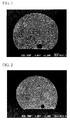
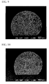
- Cross sections of these Au-Sn alloy bumps were observed using a metallographic microscope in 1000 fold magnification, and texture photographs were taken from the cross sections. The texture photographs are shown in FIGS. 1 to 11 .
- the area % of Sn-rich primary crystal phase in the cross sectional area of each of the Au-Sn alloy bumps 1 to 11 was measured using an image processing software. The results of the measurements are shown in Table 1. Further, 240 bumps were sampled for each of the Au-Sn alloy bumps 1 to 11. For each of the 240 Au-Sn alloy bumps 1 to 11, numbers and diameters of voids included in the bump were measured using a transmission X-ray apparatus.
- each of the voids were classified into four groups, namely, voids having a diameter of not greater than 10% of the bump diameter, voids having a diameter of greater than 10% and not greater than 20% of the bump diameter, voids having a diameter of greater than 20% and not greater than 30% of the bump diameter, and voids having a diameter greater than 30% of the bump diameter.
- the number of voids of each group is listed in Table 2.
Landscapes
- Chemical & Material Sciences (AREA)
- Engineering & Computer Science (AREA)
- Mechanical Engineering (AREA)
- Materials Engineering (AREA)
- Metallurgy (AREA)
- Organic Chemistry (AREA)
- Electric Connection Of Electric Components To Printed Circuits (AREA)
- Wire Bonding (AREA)
Abstract
An Au-Sn alloy bump that does not include large voids and a method of producing the same are provided. The An Au-Sn alloy bump that does not include large voids comprises a composition containing Sn: 20.5 to 23.5 mass % and the balance Au and unavoidable impurities, and a structure where 0.5 to 30 area % of Sn-rich primary crystal phase is crystallized in the matrix.
Description
- The present invention relates to an Au-Sn alloy bump including no large voids, specifically including no voids larger than 30% of the bump diameter and a method of producing the same bump.
- Au-Sn alloy solder paste is generally used in joining a substrate and semiconductor elements such as GaAs light elements, GaAs high frequency elements, and thermo-conducting elements, and in sealing of packages of fine and high-airtight requiring devices such as SAW filters and crystal oscillators. It is known that Au-Sn alloy powder included in the Au-Sn alloy solder paste is a powder of Au-Sn eutectic alloy having a composition containing 20 mass % of Sn with the balance consisting of Au and unavoidable impurities. It is also known that the Au-Sn eutectic alloy powder is generally obtained by a gas-atomizing process.
- It is known that An-Sn alloy bump may be used as electrodes or the like by forming a perforated dry film layer on a substrate, filling the Au-Sn alloy paste in the perforations of the dry film layer, subjecting the Au-Sn alloy paste to reflow melting and forming Au-Sn alloy bumps on the surface of the substrate, and removing the dry film layer (see Non Patent Reference 1).
- Non Patent Reference 1: Collected Papers of 10th Symposium on Microjoining and Assembly Technology in Electronics, Vol. 10, 2004, pp95-100 (Published on February 5, 2004 by Japan Welding Society)
- However, where the Au-Sn alloy bump is produced using the paste including the Au-Sn alloy powder having a composition containing 20 mass % of Sn with the balance consisting of Au and unavoidable impurities as described in the above-described Non Patent Reference 1, the Au-Sn bump includes large residual voids generated in the interior. When the Au-Sn alloy bump including large residual voids in the interior is used for joining a semiconductor element and a substrate or the like, the large voids also remain in the jointing. The large voids in the jointing act as an origin of cracking, and therefore reliable jointing cannot be obtained by the Au-Sn alloy solder. Where the voids included in the Au-Sn bump are small voids having a size of 30% or less of the bump diameter, reliability of the jointing is not lowered since such voids do not act as origins of cracking. Therefore, there has been a demand for Au-Sn alloy bumps that do not include large voids larger than 30% of the bump diameter.
- Therefore, the inventors conducted research for achieving a bump which does not include large voids in its interior. As a result of the research, it was found that large residual voids are depleted from the interior of Au-Sn alloy bumps, where the Au-Sn alloy bumps were obtained by reflow treatment of Au-Sn alloy solder paste produced by mixing Au-Sn alloy powder with flux, where the Au-Sn alloy powder has a composition containing Sn: 20.5 to 23.5 mass %, and the balance Au and unavoidable impurities, and a structure containing a matrix and 0.5 to 30 area 5 of Sn-rich primary crystal phase crystallized in the matrix.
- Based on the above-described research result, the present invention includes the following aspects.
- (1) An Au-Sn alloy bump which does not include large voids, having a composition containing Sn: 20.5 to 23.5 mass % with the balance consisting of Au and unavoidable impurities, and a structure where 0.5 to 30 area % of Sn-rich primary crystal phase is crystallized in the matrix.
- (2) A method of producing an Au-Sn alloy bump which does not include large voids, comprising coating in a spot-like manner a solder paste obtained by mixing Al-Sn alloy powder with flux, and subjecting the solder paste to a reflow treatment, wherein the Al-Sn alloy powder has a composition containing Sn: 20.5 to 23.5 mass %, and the balance Au and unavoidable impurities, and a structure containing 0.5 to 30 area % of Sn-rich primary crystal phase crystallized in a matrix.
- Au-Sn alloy solder paste used in the method of producing an Au-Sn alloy bump that does not includes large voids according to the present invention is prepared by the following method. Firstly, molten metal obtained by melting Au-Sn alloy having a composition containing Sn: 20.5 to 23.5 mass % and the balance consisting of Au and unavoidable impurities is maintained at a temperature of 600 to 1000°C and mechanically mixed. While mixing or after mixing the molten metal, while pressurizing the mixed molten metal at 300 to 800 kPa, the mixed molten metal is sprayed from a small-sized nozzle having a nozzle diameter of 1 to 2 mm by an inert gas at a spraying pressure of 5000 to 8000 kPa with a nozzle gap of not greater than 0.3 mm. Thus, Au-Sn alloy powder crystallizing 0.5 to 30 area % of Si-rich primary crystal phase is obtained.
It is preferable that the above-described mixing be performed by mechanical mixing. Propeller mixing is preferable as the mechanical mixing. Electric stirring such as electromagnetic stirring may be combined with the mechanical mixing. Therefore, an electromagnetic stirrer can be combined with a mechanical mixer.
The rotation speed of the above-described mechanical mixing is not limited. Preferably, the mixing is performed by a propeller mixing at 60 to 100 r.p.m for 3 to 10 minutes. In the above-described method of producing an Au-Sn alloy powder, by the mixing of the molten metal of the Au-Sn alloy, Sn-rich primary crystal phase does not grow to a large crystal, and it is possible to obtain a molten metal of Au-Sn alloy having no clusters of Au-rich primary crystal phase. By atomizing the thus obtained mixed molten metal of Au-Sn alloy, it is possible to obtain Au-Sn alloy powder which is free of Au-rich primary crystal phase and has 0.5 to 30 area % of Sn-rich primary crystal phase crystallized in the matrix. Au-Sn alloy solder paste is produced by mixing the thus obtained Au-Sn alloy powder and flux composed of commercially available rosin, active material, solvent, and thickening agent. - Where Au-Sn alloy powder is obtained by gas-atomizing a molten metal of Au-Sn alloy containing Sn: 20.5 to 23.5 mass % with the balance of Au and unavoidable impurities without mechanically mixing the molten metal, the amount of Sn-rich primary crystal phase, if any crystallization occurs, is extremely small and does not exceed 0.4 %. When a Au-Sn alloy solder paste is obtained by mixing the Au-Sn alloy powder containing a small amount of Sn-rich primary crystal phase with a commercially available flux, and bumps are obtained by coating the solder paste in a spot-like manner on a substrate and subjecting the paste on the substrates to a reflow melting, large voids larger than 30% of the bump diameter are included inside the bumps.
On the other hand, the above-described Au-Sn alloy powder having a structure showing crystallization of 0.5 to 30 area % of Sn-rich primary crystal phase and absence of Au-rich primary crystal phase can be produced by mechanically mixing a molten metal of Au-Sn alloy having a composition containing Sn: 20.5 to 23.5 mass % with the balance consisting of Au and unavoidable impurities, and atomizing the mechanically mixed Au-Sn molten alloy. In the bumps obtained by an Au-Sn alloy solder paste as a mixture of this type of Au-Sn alloy powder and commercial flux on a substrate in a spot-like manner and subjecting the paste coated on the substrate to a reflow melting, the number of voids included inside the bump is reduced, and generation of large voids exceeding 30% of the bump diameter is completely avoided. - In the present invention, the content of Sn included in the Au-Sn alloy bump was limited to 20.5 to 23.5 mass % based on the following reason. If the content of Sn included in the bump is less than 20.5 mass %, it is not preferable since Au-rich primary crystal phase crystallizes, increasing the melting point and viscosity of the melt, and gas generated during the melting of the paste is trapped in the vicinity of the substrate, causing residual voids inside the bumps. On the other hand, where the content of Sn exceeds 23.5 mass %, it is not preferable since large Sn rich primary crystal phase crystallizes even when the molten metal is mechanically mixed, and Sn-rich primary crystal phase crystallizes in an amount exceeding 30 area %, causing difficulty in escapement of voids from the interior of the bump and resulting in residual voids included in the bump.
- The amount of Sn-rich primary crystal phase crystallizing in the Au-Sn alloy powder included Au-Sn alloy paste used in the production of Au-Sn alloy bump of the present invention was limited to 0.5 to 30 area % based on the following reason. Where the amount of Sn-rich primary crystal phase crystallizing in the Au-Sn powder is less than 0.5% in a section of the Au-Sn powder, it is not preferable since crystallization of Au-rich primary crystal phase occurs. Since the Au-rich primary crystal phase has a high melting point compared to other eutectic structures, the viscosity of the melt is increased at the same temperature, and the gas generated during melting of the paste is trapped, causing generation of voids. Where the amount of Sn-rich primary crystal phase crystallizing in the Au-Sn powder is more than 30% in a section of the Au-Sn powder, it is not preferable since the melting point apparently shifts to a high temperature. By the increased proportion of the Sn-rich primary crystal phase and melting point shifting from the eutectic point, melting point is increased, viscosity of the melt is increased, and flowability of the melt is decreased. As a result, gas generated during melting of the paste is trapped, causing generation of voids.
A more preferable range for the amount of Sn-rich primary crystal phase crystallizing in the Au-Sn alloy powder included in the Au-Sn alloy paste used in the production of Au-Sn alloy bump of the present invention is 10 to 20 area %. - Since the Au-Sn alloy bump of the present invention does not include large voids larger than 30% of the bump diameter, compared to the conventional Au-Sn alloy bump, there is a lower possibility of causing generation of cracks starting from voids, and the joint portion has a high reliability. Therefore, the proportion of defective products of semiconductor devices is decreased, enabling reduction of cost. Thus, the present invention provides an excellent industrial effect.
-
-
FIG. 1 is a metallographic microscopy photograph of a section of Au-Sn alloy bump 1. -
FIG. 2 is a metallographic microscopy photograph of a section of Au-Sn alloy bump 2. -
FIG. 3 is a metallographic microscopy photograph of a section of Au-Sn alloy bump 3. -
FIG. 4 is a metallographic microscopy photograph of a section of Au-Sn alloy bump 4. -
FIG. 5 is a metallographic microscopy photograph of a section of Au-Sn alloy bump 5. -
FIG. 6 is a metallographic microscopy photograph of a section of Au-Sn alloy bump 6. -
FIG. 7 is a metallographic microscopy photograph of a section of Au-Sn alloy bump 7. -
FIG. 8 is a metallographic microscopy photograph of a section of Au-Sn alloy bump 8. -
FIG. 9 is a metallographic microscopy photograph of a section of Au-Sn alloy bump 9. -
FIG. 10 is a metallographic microscopy photograph of a section of Au-Sn alloy bump 10. -
FIG. 11 is a metallographic microscopy photograph of a section of Au-Sn alloy bump 11. - Au-Sn alloys having compositions shown in Table 1 were made molten in a high frequency melting furnace. While maintaining the molten metal of each alloy at a temperature shown in Table 1, the molten metal was mechanically mixed by a propeller revolving at a cycle shown in Table 1 for a duration shown in Table 1. While mixing or after mixing each molten metal, a pressure shown in Table 1 was applied to the molten metal, thereby dropping the molten metal from a nozzle provided to a bottom of the high frequency melting furnace. At the same time, from gas nozzles that had a diameter shown in Table 1 and were provided around the nozzle such that the nozzle gap was 0.2 mm, Ar gas was injected to the dropping molten metal with an injection pressure shown in Table 1. Thus gas atomized powders were produced. By sieving each gas atomized powder using a sieve, Au-Sn alloy powders having an average grain size of 20FLm were produced.
- Each of these Au-Sn alloy powders was embedded in a resin. After polishing a section of the resin, an EPMA photograph was taken from the section. Ten powder particles having a particle section diameter of 15FLm were randomly sampled from the EPMA image, and the area % of Sn-rich primary crystal phase in a section area of the powder was obtained using an image processing software. The results are shown in Table 1.
Commercial RMA flux was mixed with each of the Au-Sn alloy powders such that the flux ratio was 7 mass %. Thus, Au-Sn alloy solder pastes 1 to 1 were produced. - Next, the following measurements were performed using these Au-Sn alloy solder pastes 1-11.
Firstly, plates made of Si, each having a dimension of 10 mm in length, 10 mm in width, and 1 mm in thickness were produced. After forming an Al-sputtered film of 0.5 µm in thickness on a surface of each plate, a Ni-V alloy sputtered film of 0.5 µm in thickness was formed on the Al-sputtered film, and a Cu-sputtered film of 1.0FLm was formed thereon. A dry film layer having a thickness of 70FLm and holes of 95FLm in diameter was formed on the plates each having the Cu-sputtered film. The above-described Au-Sn alloy solder pastes 1 to 11 were filled in the holes of the dry film layer and subjected to reflow treatment (preliminary heating at 150°C for 60 seconds and main heating at 320°C for 60 seconds). Thus, Au-Sn alloy bumps 1 to 11 were produced. For each of Au-Sn bumps 1 to 11, 1000 bumps each having a diameter of 80FLm and a height of 60FLm were produced.
Cross sections of these Au-Sn alloy bumps were observed using a metallographic microscope in 1000 fold magnification, and texture photographs were taken from the cross sections. The texture photographs are shown inFIGS. 1 to 11 . After that, using the above-described texture photographs, the area % of Sn-rich primary crystal phase in the cross sectional area of each of the Au-Sn alloy bumps 1 to 11 was measured using an image processing software. The results of the measurements are shown in Table 1. Further, 240 bumps were sampled for each of the Au-Sn alloy bumps 1 to 11. For each of the 240 Au-Sn alloy bumps 1 to 11, numbers and diameters of voids included in the bump were measured using a transmission X-ray apparatus.
Based on the proportion of the void diameters to the bump diameters, each of the voids were classified into four groups, namely, voids having a diameter of not greater than 10% of the bump diameter, voids having a diameter of greater than 10% and not greater than 20% of the bump diameter, voids having a diameter of greater than 20% and not greater than 30% of the bump diameter, and voids having a diameter greater than 30% of the bump diameter. The number of voids of each group is listed in Table 2. -

-

- From the results shown in
FIGS. 1 to 11 and Table 2, the following can be understood. Large voids exceeding 30% of the bump diameter are not generated in Au-Sn alloy bumps 4 to 8 (Inventive bumps according to the present invention) containing Sn: 20.5 to 23.5 mas %. Au-Sn alloy bumps 1 to 2 (Comparative bumps) containing Sn: 18.1 to 18.9 mass %, Au-Sn alloy bump 3 (Conventional bump) containing Sn: 20.1 mass %, and Au-Sn alloy bumps 9 to 11 (Comparative bumps) containing Sn: 24.1 to 30.0 mass % are not preferable since each of them generates large voids exceeding 30% of the bump diameter.
Claims (2)
- An Au-Sn alloy bump which does not include large voids, comprising a composition containing Sn: 20.5 to 23.5 mass % with the balance consisting of Au and unavoidable impurities, and a structure where 0.5 to 30 area % of Sn-rich primary crystal phase is crystallized in a matrix.
- A method of producing an Au-Sn alloy bump which does not include large voids, comprising coating in a spot-like manner a solder paste obtained by mixing Al-Sn alloy powder with flux, and subjecting the solder paste to a reflow treatment, wherein the Al-Sn alloy powder has a composition containing Sn: 20.5 to 23.5 mass %, and the balance Au and unavoidable impurities, and a structure containing 0.5 to 30 area 5 of Sn-rich primary crystal phase crystallized in a matrix.
Applications Claiming Priority (2)
| Application Number | Priority Date | Filing Date | Title |
|---|---|---|---|
| JP2005336084A JP4826735B2 (en) | 2005-11-21 | 2005-11-21 | Manufacturing method of Au-Sn alloy bump without incorporating large voids |
| PCT/JP2005/021838 WO2007057982A1 (en) | 2005-11-21 | 2005-11-29 | Au-Sn ALLOY BUMP HAVING NO TRAPPED-IN LARGE VOID AND PROCESS FOR PRODUCING THE SAME |
Publications (2)
| Publication Number | Publication Date |
|---|---|
| EP1953811A1 true EP1953811A1 (en) | 2008-08-06 |
| EP1953811A4 EP1953811A4 (en) | 2009-04-01 |
Family
ID=38048374
Family Applications (1)
| Application Number | Title | Priority Date | Filing Date |
|---|---|---|---|
| EP05811709A Withdrawn EP1953811A4 (en) | 2005-11-21 | 2005-11-29 | ALUMINUM PEEL ALLOY WITHOUT EMPTY VACUUM EMPRISONNE AND PROCESS FOR MANUFACTURING SAID PEARL |
Country Status (7)
| Country | Link |
|---|---|
| US (1) | US8721961B2 (en) |
| EP (1) | EP1953811A4 (en) |
| JP (1) | JP4826735B2 (en) |
| KR (1) | KR101235540B1 (en) |
| CN (1) | CN101313396B (en) |
| TW (1) | TW200720004A (en) |
| WO (1) | WO2007057982A1 (en) |
Families Citing this family (5)
| Publication number | Priority date | Publication date | Assignee | Title |
|---|---|---|---|---|
| CN102047397B (en) * | 2008-06-12 | 2013-10-16 | 三菱综合材料株式会社 | Bonding method of substrate and weldment using solder paste |
| US20110270099A1 (en) * | 2010-04-28 | 2011-11-03 | Medtronic, Inc. | Hermetic wafer-to-wafer bonding with electrical interconnection |
| US8513120B2 (en) | 2010-04-29 | 2013-08-20 | Medtronic, Inc. | Gold-tin etch using combination of halogen plasma and wet etch |
| US10612112B2 (en) | 2015-04-09 | 2020-04-07 | Electronics And Telecommunications Research Institute | Noble metal material for 3-dimensional printing, method for manufacturing the same, and method for 3-dimensional printing using the same |
| KR101839876B1 (en) * | 2015-04-09 | 2018-03-20 | 한국전자통신연구원 | Noble metal material for 3-dimension printing, method for fabricating the same, and method for printing using the same |
Family Cites Families (13)
| Publication number | Priority date | Publication date | Assignee | Title |
|---|---|---|---|---|
| US4758272A (en) * | 1987-05-27 | 1988-07-19 | Corning Glass Works | Porous metal bodies |
| JPS6431907A (en) * | 1987-07-27 | 1989-02-02 | Nippon Kokan Kk | Apparatus for producing metal powder |
| JPH02115307A (en) * | 1988-10-25 | 1990-04-27 | Daido Steel Co Ltd | Molten metal spraying method and pouring device for the same |
| JPH04262895A (en) | 1991-02-15 | 1992-09-18 | Tanaka Kikinzoku Kogyo Kk | Manufacture of metallic ultra fine ball |
| JP3446798B2 (en) | 1996-11-29 | 2003-09-16 | 日本特殊陶業株式会社 | Wiring board with bonding bump |
| EP0915639A1 (en) | 1999-01-05 | 1999-05-12 | Phonak Ag | Method for binaural adjusting of hearing aids |
| CN1157497C (en) * | 2000-04-12 | 2004-07-14 | 林忠华 | Self-catalytic plating Ni-Sn-P alloy solution and its plated layer |
| JP2001176999A (en) * | 2000-11-27 | 2001-06-29 | Tanaka Kikinzoku Kogyo Kk | Hermetic sealing method for electronic components |
| JP4051661B2 (en) * | 2001-09-28 | 2008-02-27 | 三菱マテリアル株式会社 | Au-Sn alloy powder for solder paste |
| JP2003260588A (en) * | 2002-03-08 | 2003-09-16 | Mitsubishi Materials Corp | Au-Sn alloy powder for solder paste with little wet spread |
| JP4769469B2 (en) * | 2004-02-20 | 2011-09-07 | 田中貴金属工業株式会社 | Bonding method using Au-Sn brazing material |
| KR101141089B1 (en) | 2004-06-28 | 2012-05-03 | 미쓰비시 마테리알 가부시키가이샤 | Au-Sn ALLOY POWDER FOR SOLDER PASTE |
| JP4560830B2 (en) | 2004-06-28 | 2010-10-13 | 三菱マテリアル株式会社 | Au-Sn alloy powder for solder paste |
-
2005
- 2005-11-21 JP JP2005336084A patent/JP4826735B2/en not_active Expired - Lifetime
- 2005-11-28 TW TW094141743A patent/TW200720004A/en not_active IP Right Cessation
- 2005-11-29 US US12/094,167 patent/US8721961B2/en active Active
- 2005-11-29 WO PCT/JP2005/021838 patent/WO2007057982A1/en not_active Ceased
- 2005-11-29 CN CN2005800521116A patent/CN101313396B/en not_active Expired - Lifetime
- 2005-11-29 EP EP05811709A patent/EP1953811A4/en not_active Withdrawn
- 2005-11-29 KR KR1020087011683A patent/KR101235540B1/en not_active Expired - Lifetime
Also Published As
| Publication number | Publication date |
|---|---|
| JP4826735B2 (en) | 2011-11-30 |
| TWI341225B (en) | 2011-05-01 |
| TW200720004A (en) | 2007-06-01 |
| EP1953811A4 (en) | 2009-04-01 |
| US8721961B2 (en) | 2014-05-13 |
| KR101235540B1 (en) | 2013-02-21 |
| WO2007057982A1 (en) | 2007-05-24 |
| CN101313396A (en) | 2008-11-26 |
| US20080304999A1 (en) | 2008-12-11 |
| JP2007136523A (en) | 2007-06-07 |
| KR20080069187A (en) | 2008-07-25 |
| CN101313396B (en) | 2010-05-12 |
Similar Documents
| Publication | Publication Date | Title |
|---|---|---|
| JPWO2019172410A1 (en) | Flux, solder paste, soldering process, soldering product manufacturing method, BGA package manufacturing method | |
| JP4560830B2 (en) | Au-Sn alloy powder for solder paste | |
| US8721961B2 (en) | Au—Sn alloy bump including no large void and method of producing same | |
| JP2013237089A (en) | Solder alloy powder and solder paste for bump, and solder bump using the same | |
| KR20170074913A (en) | Sealing paste, brazing material and production method thereof, sealing lid member and production method thereof, and package sealing method | |
| JP6070927B2 (en) | Au-Sn alloy-containing paste, Au-Sn alloy thin film and film forming method thereof | |
| KR20150088811A (en) | Au-sn-bi alloy powder paste, au-sn-bi alloy thin film, and method for forming au-sn-bi alloy thin film | |
| JP5077690B2 (en) | Au-Sn alloy solder paste for printing | |
| JP4811661B2 (en) | Au-Sn alloy solder paste with less void generation | |
| JP6511773B2 (en) | Au-Sn alloy solder paste, method of manufacturing Au-Sn alloy solder paste, method of manufacturing Au-Sn alloy solder layer | |
| CN1275734C (en) | Lead-less joining material and joining method using such material | |
| KR101141089B1 (en) | Au-Sn ALLOY POWDER FOR SOLDER PASTE | |
| JP2013237090A (en) | Solder alloy powder for bump, paste and solder bump using the same | |
| JP4872764B2 (en) | Au-Sn alloy solder paste with less void generation | |
| JP4780464B2 (en) | Au-Ge alloy solder paste | |
| JP5003551B2 (en) | Pb-Sn solder alloy powder for paste and Pb-Sn solder alloy ball | |
| JP2017177122A (en) | High temperature Pb-free solder paste and manufacturing method thereof | |
| JP4780466B2 (en) | Sn-Au alloy solder paste for Au plated substrate | |
| JPH0596396A (en) | Cream solder | |
| JP2003224157A (en) | Electronic component manufacturing method and solder ball | |
| US6416597B1 (en) | Solder composition and a method for making the same | |
| JPS62166091A (en) | cream solder |
Legal Events
| Date | Code | Title | Description |
|---|---|---|---|
| PUAI | Public reference made under article 153(3) epc to a published international application that has entered the european phase |
Free format text: ORIGINAL CODE: 0009012 |
|
| 17P | Request for examination filed |
Effective date: 20080521 |
|
| AK | Designated contracting states |
Kind code of ref document: A1 Designated state(s): DE |
|
| RBV | Designated contracting states (corrected) |
Designated state(s): DE |
|
| A4 | Supplementary search report drawn up and despatched |
Effective date: 20090227 |
|
| 17Q | First examination report despatched |
Effective date: 20110207 |
|
| STAA | Information on the status of an ep patent application or granted ep patent |
Free format text: STATUS: THE APPLICATION IS DEEMED TO BE WITHDRAWN |
|
| 18D | Application deemed to be withdrawn |
Effective date: 20110618 |