EP1947502B1 - Liquid crystal display panel having power supply lines and liquid crystal display - Google Patents
Liquid crystal display panel having power supply lines and liquid crystal display Download PDFInfo
- Publication number
- EP1947502B1 EP1947502B1 EP08000836.0A EP08000836A EP1947502B1 EP 1947502 B1 EP1947502 B1 EP 1947502B1 EP 08000836 A EP08000836 A EP 08000836A EP 1947502 B1 EP1947502 B1 EP 1947502B1
- Authority
- EP
- European Patent Office
- Prior art keywords
- liquid crystal
- crystal display
- printed circuit
- circuit board
- power supply
- Prior art date
- Legal status (The legal status is an assumption and is not a legal conclusion. Google has not performed a legal analysis and makes no representation as to the accuracy of the status listed.)
- Expired - Fee Related
Links
Images


Classifications
-
- G—PHYSICS
- G02—OPTICS
- G02F—OPTICAL DEVICES OR ARRANGEMENTS FOR THE CONTROL OF LIGHT BY MODIFICATION OF THE OPTICAL PROPERTIES OF THE MEDIA OF THE ELEMENTS INVOLVED THEREIN; NON-LINEAR OPTICS; FREQUENCY-CHANGING OF LIGHT; OPTICAL LOGIC ELEMENTS; OPTICAL ANALOGUE/DIGITAL CONVERTERS
- G02F1/00—Devices or arrangements for the control of the intensity, colour, phase, polarisation or direction of light arriving from an independent light source, e.g. switching, gating or modulating; Non-linear optics
- G02F1/01—Devices or arrangements for the control of the intensity, colour, phase, polarisation or direction of light arriving from an independent light source, e.g. switching, gating or modulating; Non-linear optics for the control of the intensity, phase, polarisation or colour
- G02F1/13—Devices or arrangements for the control of the intensity, colour, phase, polarisation or direction of light arriving from an independent light source, e.g. switching, gating or modulating; Non-linear optics for the control of the intensity, phase, polarisation or colour based on liquid crystals, e.g. single liquid crystal display cells
- G02F1/133—Constructional arrangements; Operation of liquid crystal cells; Circuit arrangements
- G02F1/1333—Constructional arrangements; Manufacturing methods
- G02F1/1345—Conductors connecting electrodes to cell terminals
- G02F1/13452—Conductors connecting driver circuitry and terminals of panels
-
- G—PHYSICS
- G02—OPTICS
- G02F—OPTICAL DEVICES OR ARRANGEMENTS FOR THE CONTROL OF LIGHT BY MODIFICATION OF THE OPTICAL PROPERTIES OF THE MEDIA OF THE ELEMENTS INVOLVED THEREIN; NON-LINEAR OPTICS; FREQUENCY-CHANGING OF LIGHT; OPTICAL LOGIC ELEMENTS; OPTICAL ANALOGUE/DIGITAL CONVERTERS
- G02F1/00—Devices or arrangements for the control of the intensity, colour, phase, polarisation or direction of light arriving from an independent light source, e.g. switching, gating or modulating; Non-linear optics
- G02F1/01—Devices or arrangements for the control of the intensity, colour, phase, polarisation or direction of light arriving from an independent light source, e.g. switching, gating or modulating; Non-linear optics for the control of the intensity, phase, polarisation or colour
- G02F1/13—Devices or arrangements for the control of the intensity, colour, phase, polarisation or direction of light arriving from an independent light source, e.g. switching, gating or modulating; Non-linear optics for the control of the intensity, phase, polarisation or colour based on liquid crystals, e.g. single liquid crystal display cells
- G02F1/133—Constructional arrangements; Operation of liquid crystal cells; Circuit arrangements
- G02F1/1333—Constructional arrangements; Manufacturing methods
- G02F1/1345—Conductors connecting electrodes to cell terminals
-
- G—PHYSICS
- G02—OPTICS
- G02F—OPTICAL DEVICES OR ARRANGEMENTS FOR THE CONTROL OF LIGHT BY MODIFICATION OF THE OPTICAL PROPERTIES OF THE MEDIA OF THE ELEMENTS INVOLVED THEREIN; NON-LINEAR OPTICS; FREQUENCY-CHANGING OF LIGHT; OPTICAL LOGIC ELEMENTS; OPTICAL ANALOGUE/DIGITAL CONVERTERS
- G02F1/00—Devices or arrangements for the control of the intensity, colour, phase, polarisation or direction of light arriving from an independent light source, e.g. switching, gating or modulating; Non-linear optics
- G02F1/01—Devices or arrangements for the control of the intensity, colour, phase, polarisation or direction of light arriving from an independent light source, e.g. switching, gating or modulating; Non-linear optics for the control of the intensity, phase, polarisation or colour
- G02F1/13—Devices or arrangements for the control of the intensity, colour, phase, polarisation or direction of light arriving from an independent light source, e.g. switching, gating or modulating; Non-linear optics for the control of the intensity, phase, polarisation or colour based on liquid crystals, e.g. single liquid crystal display cells
- G02F1/133—Constructional arrangements; Operation of liquid crystal cells; Circuit arrangements
- G02F1/1333—Constructional arrangements; Manufacturing methods
- G02F1/1335—Structural association of cells with optical devices, e.g. polarisers or reflectors
- G02F1/1336—Illuminating devices
- G02F1/133615—Edge-illuminating devices, i.e. illuminating from the side
-
- G—PHYSICS
- G02—OPTICS
- G02F—OPTICAL DEVICES OR ARRANGEMENTS FOR THE CONTROL OF LIGHT BY MODIFICATION OF THE OPTICAL PROPERTIES OF THE MEDIA OF THE ELEMENTS INVOLVED THEREIN; NON-LINEAR OPTICS; FREQUENCY-CHANGING OF LIGHT; OPTICAL LOGIC ELEMENTS; OPTICAL ANALOGUE/DIGITAL CONVERTERS
- G02F1/00—Devices or arrangements for the control of the intensity, colour, phase, polarisation or direction of light arriving from an independent light source, e.g. switching, gating or modulating; Non-linear optics
- G02F1/01—Devices or arrangements for the control of the intensity, colour, phase, polarisation or direction of light arriving from an independent light source, e.g. switching, gating or modulating; Non-linear optics for the control of the intensity, phase, polarisation or colour
- G02F1/13—Devices or arrangements for the control of the intensity, colour, phase, polarisation or direction of light arriving from an independent light source, e.g. switching, gating or modulating; Non-linear optics for the control of the intensity, phase, polarisation or colour based on liquid crystals, e.g. single liquid crystal display cells
- G02F1/133—Constructional arrangements; Operation of liquid crystal cells; Circuit arrangements
- G02F1/1333—Constructional arrangements; Manufacturing methods
- G02F1/1335—Structural association of cells with optical devices, e.g. polarisers or reflectors
- G02F1/1336—Illuminating devices
- G02F1/133602—Direct backlight
- G02F1/133612—Electrical details
Definitions
- the present invention relates to a liquid crystal display panel having power supply lines and, more specifically, to a liquid crystal display panel having power supply lines formed on a substrate to supply power to a light source and to a liquid crystal display including the liquid crystal display panel.
- Lamp types of line light sources such as a cold cathode fluorescent lamp and an external electrode fluorescent lamp, have been used for backlight units for notebook computers.
- a reflecting plate is used with the lamp type of line light source, and the thickness of an optical waveguide corresponding to the thickness of the lamp is used, which results in an increase in the thickness and weight of a module.
- a high voltage induction inverter is used to turn on the lamp, resulting in an increase in power consumption.
- backlight units using light emitting diodes as light sources have been used.
- the use of the light emitting diode in the backlight unit makes it possible to reduce the thickness and power consumption of the backlight unit and to improve the brightness and color reproducibility.
- a data driver and a light source of the backlight unit are arranged opposite to each other with a liquid crystal display panel interposed therebetween, and the data driver is bent toward the rear side of the liquid crystal display panel.
- a flexible printed circuit board is used to connect the light source and a power supply mounted on a printed circuit board of the data driver in order to supply power to the light source unit.
- the printed circuit board of the data driver is far from the light source unit, a flexible printed circuit board having a large length is needed, which results in an increase in the manufacturing costs of the flexible printed circuit board.
- the flexible printed circuit board having a large length may not be taut and may be bent.
- US 2005/019033-A1 discloses a liquid crystal panel according to the preamble of claim 1.
- Embodiments of the invention to provide a liquid crystal panel having power supply lines formed on a substrate to supply power to a backlight unit and a liquid crystal display including the liquid crystal display panel.
- a liquid crystal display panel includes a first substrate including a plurality of gate lines, a plurality of data lines that are formed so as to intersect the plurality of gate lines while being insulated therefrom, and a plurality of pixels that are formed between the plurality of gate lines and the plurality of data lines, a second substrate that faces the first substrate and includes a plurality of color filters, a power supply unit that supplies power to a light source, power supply lines that are formed on the first substrate so as to be electrically connected to the power supply unit, and a flexible printed circuit board that is electrically connected to the power supply lines.
- the liquid crystal display panel further includes a data driver that applies data signals to the plurality of data lines, and a gate driver that applies gate signals to the plurality of gate lines.
- the liquid crystal display panel may further include a connector that is formed at one end of the flexible printed circuit board.
- the data driver includes a data driving IC that generates data signals, a printed circuit board having the power supply unit mounted thereon, and a film that electrically connects the printed circuit board and the first substrate and has the data driving IC mounted thereon.
- the data driver may be arranged on a first side of the first substrate, and the gate driver is arranged on a second side of the first substrate adjacent to the first side.
- the power supply lines may be formed on the first substrate along the second side.
- the power supply lines may be formed on the first substrate along a third side opposite to the second side.
- the power supply lines may be formed on the first substrate along the second side and a third side opposite to the second side.
- the liquid crystal display panel may comprise another flexible printed circuit in addition to the flexible printed circuit board, wherein the flexible printed circuit board is connected to the power supply lines formed on the first substrate along the second side and the other flexible printed circuit board is connected to the power supply lines along the third side.
- the gate driver may include a gate driving IC that generates gate signals.
- the gate driver may further include a film having the gate driving IC mounted thereon, and the film may be arranged on the first substrate.
- the liquid crystal display panel may further include control signal lines that are formed on the first substrate and through which control signals required to operate the gate driving IC are supplied.
- the liquid crystal display panel may further include first connection lines that are formed on the second film and electrically connect the power supply lines to the gate driving IC, and second connection lines that are formed on the second film and electrically connect the control signal lines to the gate driving IC.
- the gate driver may be formed on the first substrate, and include a shift register composed of a plurality of stages for outputting the gate signals.
- a liquid crystal display includes a liquid crystal display panel including a first substrate having a plurality of gate lines, a plurality of data lines that are formed so as to intersect the plurality of gate lines while being insulated therefrom, and a plurality of pixels that are formed between the plurality of gate lines and the plurality of data lines, a second substrate that faces the first substrate and includes a plurality of color filters, a power supply unit, power supply lines that are formed on the first substrate so as to be electrically connected to the power supply unit, and a first flexible printed circuit board that is electrically connected to the power supply lines.
- the liquid crystal display further includes a backlight unit including a light emitting diode and a second flexible printed circuit board having the light emitting diode mounted thereon, the second flexible printed circuit board being electrically connected to the first flexible printed circuit board, wherein the power supply unit supplies power to the light emitting diode.
- the liquid crystal display may further include a data driver that applies data signals to the plurality of data lines, and a gate driver that applies gate signals to the plurality of gate lines.
- the liquid crystal display may further include a first connector that is formed at an end of the first flexible printed circuit board, and a second connector that is formed at an end of the second flexible printed circuit board and is connected to the first connector.
- the data driver may be arranged on a first side of the first substrate, and the gate driver may be arranged on a second side of the first substrate adjacent to the first side.
- the power supply lines may be formed on the first substrate along the second side.
- the power supply lines may be formed on the first substrate along a third side opposite to the second side.
- the power supply lines may be formed on the first substrate along the second side and a third side opposite to the second side.
- the backlight unit may be arranged on a fourth side of the first substrate opposite to the first side.
- Fig. 1 is a diagram schematically illustrating the structure of a liquid crystal display according to an embodiment of the invention.
- a liquid crystal display panel 1000 includes a thin film transistor (TFT substrate 100, a color filter substrate 200, a data driver 300, a gate driver 400, power supply lines 500, a first flexible printed circuit board 600, and a first connector 700.
- a backlight unit 2000 provided on one side of the liquid crystal display panel 1000 includes a second flexible printed circuit board 1100, a second connector 1200, and light emitting diodes 1300.
- the liquid crystal display panel 1000 includes the TFT substrate 100, which is a lower substrate, the color filter substrate 200, which is an upper substrate positioned opposite the TFT substrate 100, and a liquid crystal layer (not shown) that is interposed between the two substrates and contains liquid crystal molecules aligned in a predetermined direction with respect to the two substrates.
- the TFT substrate 100 includes a plurality of gate lines (not shown) formed in a first direction, for example, in a horizontal direction, a plurality of data lines (not shown) that are formed so as to intersect the gate lines, while being insulated therefrom, and a plurality of pixels (not shown) formed between the plurality of gate lines and the plurality of data lines.
- Each of the unit pixels includes a switching element, that is, a TFT, a pixel electrode, and a storage capacitor electrode.
- the TFT allows a data signal supplied to the data line to be charged to the pixel electrode in response to a gate signal supplied to the gate line.
- the color filter substrate 200 includes a black matrix (not shown) for preventing light leakage and light interference between adjacent pixels, red, green, and blue color filters (not shown), and a common electrode (not shown) formed of a transparent conductive material.
- the data driver 300 applies predetermined data signals to the data lines
- the gate driver 400 applies predetermined gate signals to the gate lines.
- the data driver 300 includes a data driving IC 310 for generating data signals, a printed circuit board 320 having various circuit parts including a power supply unit 325 mounted thereon, and a first film 330 that electrically connects the printed circuit board 320 to the TFT substrate 100 and has the data driving IC 310 mounted thereon.
- the gate driver 400 includes a gate driving IC 410 for generating gate signals and a second film 420 that is arranged on the TFT substrate 100 and has the gate driving IC 410 mounted thereon.
- the data driver 300 is arranged on the upper side of the TFT substrate, and the gate driver 400 is arranged on the left or right side of the TFT substrate (in this embodiment, on the left side of the TFT substrate).
- the power supply lines 500 are formed on the TFT substrate 100 along one side thereof (in this embodiment) a left side) to supply power from the power supply unit 325 mounted on the printed circuit board 320 of the data driver 300 to the light emitting diodes 1300 of the backlight unit 2000.
- each of the power supply lines 500 is connected to the power supply unit 325 through a circuit pattern (not shown) formed on the printed circuit board 320, and the other end thereof is electrically connected to the first flexible printed circuit board 600.
- the first connector 700 is formed at the end of the first flexible printed circuit board 600.
- the backlight unit 2000 is arranged on a lower side of the liquid crystal display panel 1000, that is, on the opposite side of the data driver 300.
- the light emitting diodes 1300 are mounted on the second flexible printed circuit board 1100.
- the second flexible printed circuit board 1100 has a portion protruding from one side thereof, and the second connector 1200 is formed at the end of the protruding portion.
- the first connector 700 formed at the end of the first flexible printed circuit board 600 is coupled and electrically connected to the second connector 1200 formed at the end of the protruding portion of the second flexible printed circuit board 1100.
- power output from the power supply unit 325 is applied to the light emitting diodes 1300 through the power supply lines 500 formed on the TFT substrate 100, the first flexible printed circuit board 600, the first connector 700, the second connector 1200, and the second flexible printed circuit board 1100.
- the power supply lines formed on the TFT substrate make it possible to reduce the length of the flexible printed circuit board, as compared to the related art in which the power supply unit is connected to the backlight unit using the flexible printed circuit board. As a result, it is possible to reduce manufacturing costs of the flexible printed circuit board and prevent the flexible printed circuit board from bending or lacking tautness, which makes it possible to smoothly supply power from the power supply unit to the light emitting diodes.
- Fig. 2 is a plan view illustrating the liquid crystal display panel of the liquid crystal display shown in Fig. 1 .
- the data driver 300 is arranged on the upper side of the TFT substrate, and the gate driver 400 is arranged on the left side of the TFT substrate.
- various circuit parts (not shown) required to drive the liquid crystal display panel are mounted on the printed circuit board 320 of the data driver 300.
- a timing controller that generates control signals for controlling the gate driver and the data driver and controls digital data signals input from, for example, a computer, and a gamma standard voltage generator that outputs the grayscale of the data driver as a voltage may be mounted on the printed circuit board 320 of the data driver 300.
- the gate driver 400 includes the gate driving IC 410 for generating gate signals, the second film 420 having the gate driving IC 410 mounted thereon, and control signal lines 450.
- the control signal lines 450 are formed on the TFT substrate 100 along one side thereof, for example, along the left side, and the power supply lines 500 are formed on the TFT substrate 100 along one side thereof, for example, the left side, to supply power from the power supply unit 325 mounted on the printed circuit board 320 of the data driver 300 to the light emitting diodes 1300 of the backlight unit 2000.
- the power supply lines 500 are formed at a predetermined distance from the control signal lines 450.
- First connection lines 430 and second connection lines 440 are formed on the second film 420 having the gate driving IC 410 mounted thereon.
- One end of each of the first connection lines 430 is electrically connected to the corresponding power supply line 500, and the other ends thereof are electrically connected to the gate driving IC 410.
- One end of each of the second connection lines 440 is electrically connected to the corresponding control signal line 450, and the other ends thereof are electrically connected to the gate driving IC 410.
- power output from the power supply unit 325 is supplied to the first flexible printed circuit board 600 and the first connector 700 through a sequential path including the power supply lines 500, the first connection lines 430, the gate driving IC 410, the first connection lines 430, and the power supply lines 500 and so on, continuing based on the number gate driving ICs 410.
- the gate driving IC 410 is connected to the TFT substrate 100 by a COF (chip on film) technique using a film or a TCP (tape carrier package) manner, but the embodiments of the invention are not limited thereto.
- the gate driving IC 410 may be directly mounted on the TFT substrate 100 by a COG (chip on glass) technique.
- the second film 420 and the first and second connection lines 430 and 440 may be omitted.
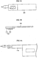
- Figs. 3A and 3B are a plan view and a side view illustrating the first flexible printed circuit board 600 of the liquid crystal display panel, respectively, and Figs. 4A and 4B are a plan view and a side view illustrating the second flexible printed circuit board 1100 of the backlight unit, respectively.
- Fig. 5 is a cross-sectional view illustrating coupling between the first connector 700 and the second connector 1200.
- the first connector 700 is formed on one side of the first flexible printed circuit board 600 of the liquid crystal display panel
- the second connector 1200 is formed on one side of the second flexible printed circuit board 1100 of the backlight unit.
- the first connector 700 includes a first base plate 710 and a convex terminal 720 that protrudes from the fust base plate 710 to a predetermined height.
- a circuit pattern (not shown) connected to the power supply line 500 (see Figs. 1 and 2 ) is formed on the first printed circuit board 600 to be electrically connected to the convex terminal 720 through the first base plate 710.
- the second connector 1200 includes a second base plate 1210 and a concave terminal 1220 that is recessed into the second base plate 1210 to a predetermined depth.
- the convex terminal 720 of the first connector 700 and the concave terminal 1220 of the second connector 1200 are formed so as to mate with each other, and the convex terminal 720 is coupled into the concave terminal 1220.
- the convex terminal 720 is formed on the first connector 700
- the concave terminal 1220 is formed in the second connector 1200, but the embodiments of the invention are not limited thereto.
- a convex terminal may be formed on the second connector 1200, and a concave terminal may be formed in the first connector 700.
- the fitting structure between the first connector and the second connector is not limited to the above, but various structures for connecting the first terminal to the second terminal may be used.
- Fig. 6 is a diagram schematically illustrating the structure of a liquid crystal display according to an embodiment of the invention.
- the embodiment shown in Fig. 6 is substantially similar to the embodiment described in connection with Fig. 1 except for at least the positions of the power supply lines.
- the data driver 300 is arranged on the upper side of the TFT substrate
- the gate driver 400 is arranged on the left side of the TFT substrate.
- the power supply lines 500 are formed on the opposite side of the gate driver 400, that is, on the right side of the TFT substrate 100, to apply power supplied from the power supply unit 325 mounted to the printed circuit board 320 of the data driver 300 to the light emitting diodes 1300 of the backlight unit 2000.
- a high voltage of, for example, about 15 to 25 V and a current of about 100 mA may be applied to the light emitting diodes of the backlight unit.
- the gate driving IC 410 may be damaged by the high voltage and current. Therefore, the power supply lines 500 formed on the opposite side of the gate driver 400 prevent malfunction of the gate driving IC due to the high voltage and current, resulting in higher reliability.
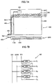
- Fig. 7A is a diagram schematically illustrating the structure of a liquid crystal display according to an embodiment of the invention
- Fig. 7B is a diagram schematically illustrating the structure of a gate driver shown in Fig. 7A .
- the embodiment shown in Figs. 7A and 7B is similar to the embodiments described in connection with Figs. 1 and 6 except for at least the structure of the gate driver.
- a gate driver 460 is provided on the TFT substrate 100 along one side thereof (in this embodiment, on the left side).
- the gate driver 460 is composed of a circuit for controlling thin film transistors, serving as switching elements for allowing external clock signals to pass through the gate lines.
- the thin film transistors are composed of amorphous silicon thin film transistors, and are formed on the substrate 100.
- the gate driver 460 includes a shift register having a plurality of cascaded stages SRC1, SRC2, SRC3, SRC4...SRC n for sequentially turning on gate lines G1, G2, G3, G4...G n , respectively, in response to a clock signal CKV and an inverted clock signal CKVB.
- SRC1, SRC2, SRC3, SRC4...SRC n for sequentially turning on gate lines G1, G2, G3, G4...G n , respectively, in response to a clock signal CKV and an inverted clock signal CKVB.
- SRC1, SRC2, SRC3, SRC4...SRC n for sequentially turning on gate lines G1, G2, G3, G4...G n , respectively, in response to a clock signal CKV and an inverted clock signal CKVB.
- Fig. 8 is a diagram schematically illustrating the structure of a liquid crystal display according to an embodiment of the invention.
- the fourth embodiment shown in Fig. 8 is similar to the embodiments described in connection with Figs. 1 , 6 and 7A-7B , except for at least the number of power supply lines and the positions thereof.
- power supply lines 500 are formed on the TFT substrate on two sides thereof opposite to each other, that is, on the left and right sides of the TFT substrate.
- the first flexible printed circuit boards 600 and the first connectors 700 are formed at ends of the power supply lines 500 formed on the left and right sides of the TFT substrate 100.
- the second connectors 1200 are formed at one end and the other end of the second flexible printed circuit board 1100 of the backlight unit 2000, and the second connectors 1200 are connected to the first connectors 700.
- the power supply lines are formed on the substrate to supply power to the backlight unit, and the flexible printed circuit board is connected to the power supply lines in the liquid crystal display panel, which makes it possible to reduce the length of the flexible printed circuit board to a minimum. As a result, it is possible to reduce the manufacturing costs of the flexible printed circuit board and prevent the flexible printed circuit board from being damaged.
Description
- The present invention relates to a liquid crystal display panel having power supply lines and, more specifically, to a liquid crystal display panel having power supply lines formed on a substrate to supply power to a light source and to a liquid crystal display including the liquid crystal display panel.
- Lamp types of line light sources, such as a cold cathode fluorescent lamp and an external electrode fluorescent lamp, have been used for backlight units for notebook computers. A reflecting plate is used with the lamp type of line light source, and the thickness of an optical waveguide corresponding to the thickness of the lamp is used, which results in an increase in the thickness and weight of a module. In addition, a high voltage induction inverter is used to turn on the lamp, resulting in an increase in power consumption.
- Therefore, in order to avoid factors such as increased thickness, weight and power consumption, backlight units using light emitting diodes as light sources have been used. The use of the light emitting diode in the backlight unit makes it possible to reduce the thickness and power consumption of the backlight unit and to improve the brightness and color reproducibility.
- In general, in the backlight unit using the light emitting diode, a data driver and a light source of the backlight unit are arranged opposite to each other with a liquid crystal display panel interposed therebetween, and the data driver is bent toward the rear side of the liquid crystal display panel. In this case, a flexible printed circuit board is used to connect the light source and a power supply mounted on a printed circuit board of the data driver in order to supply power to the light source unit. However, since the printed circuit board of the data driver is far from the light source unit, a flexible printed circuit board having a large length is needed, which results in an increase in the manufacturing costs of the flexible printed circuit board. In addition, the flexible printed circuit board having a large length may not be taut and may be bent.
-
US 2005/019033-A1 discloses a liquid crystal panel according to the preamble of claim 1. - Embodiments of the invention to provide a liquid crystal panel having power supply lines formed on a substrate to supply power to a backlight unit and a liquid crystal display including the liquid crystal display panel.
- According to the invention, a liquid crystal display panel includes a first substrate including a plurality of gate lines, a plurality of data lines that are formed so as to intersect the plurality of gate lines while being insulated therefrom, and a plurality of pixels that are formed between the plurality of gate lines and the plurality of data lines, a second substrate that faces the first substrate and includes a plurality of color filters, a power supply unit that supplies power to a light source, power supply lines that are formed on the first substrate so as to be electrically connected to the power supply unit, and a flexible printed circuit board that is electrically connected to the power supply lines.
- The liquid crystal display panel further includes a data driver that applies data signals to the plurality of data lines, and a gate driver that applies gate signals to the plurality of gate lines.
- The liquid crystal display panel may further include a connector that is formed at one end of the flexible printed circuit board.
- The data driver includes a data driving IC that generates data signals, a printed circuit board having the power supply unit mounted thereon, and a film that electrically connects the printed circuit board and the first substrate and has the data driving IC mounted thereon.
- The data driver may be arranged on a first side of the first substrate, and the gate driver is arranged on a second side of the first substrate adjacent to the first side.
- The power supply lines may be formed on the first substrate along the second side.
- The power supply lines may be formed on the first substrate along a third side opposite to the second side.
- The power supply lines may be formed on the first substrate along the second side and a third side opposite to the second side.
- The liquid crystal display panel may comprise another flexible printed circuit in addition to the flexible printed circuit board, wherein the flexible printed circuit board is connected to the power supply lines formed on the first substrate along the second side and the other flexible printed circuit board is connected to the power supply lines along the third side.
- The gate driver may include a gate driving IC that generates gate signals.
- The gate driver may further include a film having the gate driving IC mounted thereon, and the film may be arranged on the first substrate.
- The liquid crystal display panel may further include control signal lines that are formed on the first substrate and through which control signals required to operate the gate driving IC are supplied.
- The liquid crystal display panel may further include first connection lines that are formed on the second film and electrically connect the power supply lines to the gate driving IC, and second connection lines that are formed on the second film and electrically connect the control signal lines to the gate driving IC.
- The gate driver may be formed on the first substrate, and include a shift register composed of a plurality of stages for outputting the gate signals.
- According to embodiment of the invention, a liquid crystal display includes a liquid crystal display panel including a first substrate having a plurality of gate lines, a plurality of data lines that are formed so as to intersect the plurality of gate lines while being insulated therefrom, and a plurality of pixels that are formed between the plurality of gate lines and the plurality of data lines, a second substrate that faces the first substrate and includes a plurality of color filters, a power supply unit, power supply lines that are formed on the first substrate so as to be electrically connected to the power supply unit, and a first flexible printed circuit board that is electrically connected to the power supply lines. The liquid crystal display further includes a backlight unit including a light emitting diode and a second flexible printed circuit board having the light emitting diode mounted thereon, the second flexible printed circuit board being electrically connected to the first flexible printed circuit board, wherein the power supply unit supplies power to the light emitting diode.
- The liquid crystal display may further include a data driver that applies data signals to the plurality of data lines, and a gate driver that applies gate signals to the plurality of gate lines.
- The liquid crystal display may further include a first connector that is formed at an end of the first flexible printed circuit board, and a second connector that is formed at an end of the second flexible printed circuit board and is connected to the first connector.
- The data driver may be arranged on a first side of the first substrate, and the gate driver may be arranged on a second side of the first substrate adjacent to the first side.
- The power supply lines may be formed on the first substrate along the second side.
- The power supply lines may be formed on the first substrate along a third side opposite to the second side.
- The power supply lines may be formed on the first substrate along the second side and a third side opposite to the second side.
- The backlight unit may be arranged on a fourth side of the first substrate opposite to the first side.
- Embodiments of the present invention can be understood in more detail from the following descriptions taken in conjunction with the attached drawings in which:
-
Fig. 1 is a diagram schematically illustrating the structure of a liquid crystal display according to an embodiment of the invention; -
Fig, 2 is a plan view illustrating a liquid crystal display panel of the liquid crystal display shown inFig. 1 ; -
Figs. 3A and 3B are a plan view and a side view illustrating a first flexible printed circuit board of the liquid crystal display panel, respectively according to an embodiment of the present invention; -
Figs. 4A and4B are a plan view and a side view illustrating a second flexible printed circuit board of a backlight unit, respectively according to an embodiment of the present invention; -
Fig. 5 is a diagram illustrating connection between a first connector and a second connector according to an embodiment of the present; -
Fig. 6 is a diagram schematically illustrating the structure of a liquid crystal display according to an embodiment of the invention; -
Fig. 7A is a diagram schematically illustrating the structure of a liquid crystal display according to an embodiment of the invention; -
Fig. 7B is a diagram schematically illustrating the structure of a gate driver shown inFig. 7A ; and -
Fig. 8 is a diagram schematically illustrating the structure of a liquid crystal display according to an embodiment of the invention. - Exemplary embodiments of the invention are described in detail hereafter with reference to accompanying drawings. The present invention, however, is not limited to the embodiments described herein, but may be modified in a variety of ways without departing from the scope and spirit of the invention.
-
Fig. 1 is a diagram schematically illustrating the structure of a liquid crystal display according to an embodiment of the invention. - Referring to
Fig. 1 , a liquidcrystal display panel 1000 includes a thin film transistor (TFT substrate 100, acolor filter substrate 200, adata driver 300, agate driver 400,power supply lines 500, a first flexible printedcircuit board 600, and afirst connector 700. Abacklight unit 2000 provided on one side of the liquidcrystal display panel 1000 includes a second flexible printedcircuit board 1100, asecond connector 1200, andlight emitting diodes 1300. - The liquid
crystal display panel 1000 includes theTFT substrate 100, which is a lower substrate, thecolor filter substrate 200, which is an upper substrate positioned opposite theTFT substrate 100, and a liquid crystal layer (not shown) that is interposed between the two substrates and contains liquid crystal molecules aligned in a predetermined direction with respect to the two substrates. - The
TFT substrate 100 includes a plurality of gate lines (not shown) formed in a first direction, for example, in a horizontal direction, a plurality of data lines (not shown) that are formed so as to intersect the gate lines, while being insulated therefrom, and a plurality of pixels (not shown) formed between the plurality of gate lines and the plurality of data lines. Each of the unit pixels includes a switching element, that is, a TFT, a pixel electrode, and a storage capacitor electrode. The TFT allows a data signal supplied to the data line to be charged to the pixel electrode in response to a gate signal supplied to the gate line. - The
color filter substrate 200 includes a black matrix (not shown) for preventing light leakage and light interference between adjacent pixels, red, green, and blue color filters (not shown), and a common electrode (not shown) formed of a transparent conductive material. - The
data driver 300 applies predetermined data signals to the data lines, and thegate driver 400 applies predetermined gate signals to the gate lines. - In this embodiment, the
data driver 300 includes adata driving IC 310 for generating data signals, a printedcircuit board 320 having various circuit parts including apower supply unit 325 mounted thereon, and afirst film 330 that electrically connects the printedcircuit board 320 to theTFT substrate 100 and has thedata driving IC 310 mounted thereon. Thegate driver 400 includes agate driving IC 410 for generating gate signals and asecond film 420 that is arranged on theTFT substrate 100 and has thegate driving IC 410 mounted thereon. - The
data driver 300 is arranged on the upper side of the TFT substrate, and thegate driver 400 is arranged on the left or right side of the TFT substrate (in this embodiment, on the left side of the TFT substrate). - The
power supply lines 500 are formed on theTFT substrate 100 along one side thereof (in this embodiment) a left side) to supply power from thepower supply unit 325 mounted on the printedcircuit board 320 of thedata driver 300 to thelight emitting diodes 1300 of thebacklight unit 2000. - One end of each of the
power supply lines 500 is connected to thepower supply unit 325 through a circuit pattern (not shown) formed on the printedcircuit board 320, and the other end thereof is electrically connected to the first flexible printedcircuit board 600. Thefirst connector 700 is formed at the end of the first flexible printedcircuit board 600. - The
backlight unit 2000 is arranged on a lower side of the liquidcrystal display panel 1000, that is, on the opposite side of thedata driver 300. Thelight emitting diodes 1300 are mounted on the second flexible printedcircuit board 1100. The second flexible printedcircuit board 1100 has a portion protruding from one side thereof, and thesecond connector 1200 is formed at the end of the protruding portion. - The
first connector 700 formed at the end of the first flexible printedcircuit board 600 is coupled and electrically connected to thesecond connector 1200 formed at the end of the protruding portion of the second flexible printedcircuit board 1100. As a result, power output from thepower supply unit 325 is applied to thelight emitting diodes 1300 through thepower supply lines 500 formed on theTFT substrate 100, the first flexible printedcircuit board 600, thefirst connector 700, thesecond connector 1200, and the second flexible printedcircuit board 1100. - The power supply lines formed on the TFT substrate make it possible to reduce the length of the flexible printed circuit board, as compared to the related art in which the power supply unit is connected to the backlight unit using the flexible printed circuit board. As a result, it is possible to reduce manufacturing costs of the flexible printed circuit board and prevent the flexible printed circuit board from bending or lacking tautness, which makes it possible to smoothly supply power from the power supply unit to the light emitting diodes.
-
Fig. 2 is a plan view illustrating the liquid crystal display panel of the liquid crystal display shown inFig. 1 . - Referring to
Fig. 2 , thedata driver 300 is arranged on the upper side of the TFT substrate, and thegate driver 400 is arranged on the left side of the TFT substrate. - In addition to the
power supply unit 325 for supplying power to the light emitting diodes 1300 (seeFig. 1 ) of the backlight unit, various circuit parts (not shown) required to drive the liquid crystal display panel are mounted on the printedcircuit board 320 of thedata driver 300. For example, a timing controller that generates control signals for controlling the gate driver and the data driver and controls digital data signals input from, for example, a computer, and a gamma standard voltage generator that outputs the grayscale of the data driver as a voltage may be mounted on the printedcircuit board 320 of thedata driver 300. - The
gate driver 400 includes thegate driving IC 410 for generating gate signals, thesecond film 420 having thegate driving IC 410 mounted thereon, and control signal lines 450. - The
control signal lines 450 are formed on theTFT substrate 100 along one side thereof, for example, along the left side, and thepower supply lines 500 are formed on theTFT substrate 100 along one side thereof, for example, the left side, to supply power from thepower supply unit 325 mounted on the printedcircuit board 320 of thedata driver 300 to thelight emitting diodes 1300 of thebacklight unit 2000. In this embodiment, thepower supply lines 500 are formed at a predetermined distance from the control signal lines 450. -
First connection lines 430 andsecond connection lines 440 are formed on thesecond film 420 having thegate driving IC 410 mounted thereon. One end of each of thefirst connection lines 430 is electrically connected to the correspondingpower supply line 500, and the other ends thereof are electrically connected to thegate driving IC 410. One end of each of thesecond connection lines 440 is electrically connected to the correspondingcontrol signal line 450, and the other ends thereof are electrically connected to thegate driving IC 410. - According to the above-mentioned structure, power output from the
power supply unit 325 is supplied to the first flexible printedcircuit board 600 and thefirst connector 700 through a sequential path including thepower supply lines 500, thefirst connection lines 430, thegate driving IC 410, thefirst connection lines 430, and thepower supply lines 500 and so on, continuing based on the numbergate driving ICs 410. - In this embodiment, the
gate driving IC 410 is connected to theTFT substrate 100 by a COF (chip on film) technique using a film or a TCP (tape carrier package) manner, but the embodiments of the invention are not limited thereto. For example, thegate driving IC 410 may be directly mounted on theTFT substrate 100 by a COG (chip on glass) technique. When thegate driving IC 410 is mounted by the COG technique, thesecond film 420 and the first andsecond connection lines -
Figs. 3A and 3B are a plan view and a side view illustrating the first flexible printedcircuit board 600 of the liquid crystal display panel, respectively, andFigs. 4A and4B are a plan view and a side view illustrating the second flexible printedcircuit board 1100 of the backlight unit, respectively.Fig. 5 is a cross-sectional view illustrating coupling between thefirst connector 700 and thesecond connector 1200. - Referring to
Figs. 3A to 5 , thefirst connector 700 is formed on one side of the first flexible printedcircuit board 600 of the liquid crystal display panel, and thesecond connector 1200 is formed on one side of the second flexible printedcircuit board 1100 of the backlight unit. - The
first connector 700 includes afirst base plate 710 and aconvex terminal 720 that protrudes from thefust base plate 710 to a predetermined height. A circuit pattern (not shown) connected to the power supply line 500 (seeFigs. 1 and2 ) is formed on the first printedcircuit board 600 to be electrically connected to theconvex terminal 720 through thefirst base plate 710. - The
second connector 1200 includes asecond base plate 1210 and a concave terminal 1220 that is recessed into thesecond base plate 1210 to a predetermined depth. Theconvex terminal 720 of thefirst connector 700 and theconcave terminal 1220 of thesecond connector 1200 are formed so as to mate with each other, and theconvex terminal 720 is coupled into theconcave terminal 1220. In this embodiment, theconvex terminal 720 is formed on thefirst connector 700, and theconcave terminal 1220 is formed in thesecond connector 1200, but the embodiments of the invention are not limited thereto. For example, a convex terminal may be formed on thesecond connector 1200, and a concave terminal may be formed in thefirst connector 700. In addition, the fitting structure between the first connector and the second connector is not limited to the above, but various structures for connecting the first terminal to the second terminal may be used. -
Fig. 6 is a diagram schematically illustrating the structure of a liquid crystal display according to an embodiment of the invention. The embodiment shown inFig. 6 is substantially similar to the embodiment described in connection withFig. 1 except for at least the positions of the power supply lines. Referring toFig. 6 , thedata driver 300 is arranged on the upper side of the TFT substrate, and thegate driver 400 is arranged on the left side of the TFT substrate. - The
power supply lines 500 are formed on the opposite side of thegate driver 400, that is, on the right side of theTFT substrate 100, to apply power supplied from thepower supply unit 325 mounted to the printedcircuit board 320 of thedata driver 300 to thelight emitting diodes 1300 of thebacklight unit 2000. - When the
power supply lines 500 are formed on the opposite side of thegate driver 400, power is supplied from thepower supply unit 325 to thelight emitting diodes 1300 of the backlight unit through thepower supply lines 500 without passing through thegate driving IC 410. - A high voltage of, for example, about 15 to 25 V and a current of about 100 mA may be applied to the light emitting diodes of the backlight unit. The
gate driving IC 410 may be damaged by the high voltage and current. Therefore, thepower supply lines 500 formed on the opposite side of thegate driver 400 prevent malfunction of the gate driving IC due to the high voltage and current, resulting in higher reliability. -
Fig. 7A is a diagram schematically illustrating the structure of a liquid crystal display according to an embodiment of the invention, andFig. 7B is a diagram schematically illustrating the structure of a gate driver shown inFig. 7A . The embodiment shown inFigs. 7A and 7B is similar to the embodiments described in connection withFigs. 1 and6 except for at least the structure of the gate driver. - Referring to
Fig. 7A , agate driver 460 is provided on theTFT substrate 100 along one side thereof (in this embodiment, on the left side). Thegate driver 460 is composed of a circuit for controlling thin film transistors, serving as switching elements for allowing external clock signals to pass through the gate lines. The thin film transistors are composed of amorphous silicon thin film transistors, and are formed on thesubstrate 100. - Referring to
Fig. 7B , thegate driver 460 includes a shift register having a plurality of cascaded stages SRC1, SRC2, SRC3, SRC4...SRCn for sequentially turning on gate lines G1, G2, G3, G4...Gn, respectively, in response to a clock signal CKV and an inverted clock signal CKVB. When a start signal STV turns on the first stage SR1, the first stage turns on the first gate line G1 in response to the clock signal CKV, which causes the second stage SR2 to be turned on. Then, the second stage turns on the second gate line G2 in response to the inverted clock signal CKVB. The second gate line G2 in the on state turns on the third stage SRC3 and turns off the first stage SRC1. In this way, the gate lines are sequentially turned on. Similar to the embodiment described in connection withFig. 6 , power is supplied through thepower lines 500 without passing throughgate driving ICS 410. -
Fig. 8 is a diagram schematically illustrating the structure of a liquid crystal display according to an embodiment of the invention. The fourth embodiment shown inFig. 8 is similar to the embodiments described in connection withFigs. 1 ,6 and7A-7B , except for at least the number of power supply lines and the positions thereof. - Referring to
Fig. 8 ,power supply lines 500 are formed on the TFT substrate on two sides thereof opposite to each other, that is, on the left and right sides of the TFT substrate. - The first flexible printed
circuit boards 600 and thefirst connectors 700 are formed at ends of thepower supply lines 500 formed on the left and right sides of theTFT substrate 100. - The
second connectors 1200 are formed at one end and the other end of the second flexible printedcircuit board 1100 of thebacklight unit 2000, and thesecond connectors 1200 are connected to thefirst connectors 700. - As described above, according to the embodiments of the invention, the power supply lines are formed on the substrate to supply power to the backlight unit, and the flexible printed circuit board is connected to the power supply lines in the liquid crystal display panel, which makes it possible to reduce the length of the flexible printed circuit board to a minimum. As a result, it is possible to reduce the manufacturing costs of the flexible printed circuit board and prevent the flexible printed circuit board from being damaged.
- Although exemplary embodiments of the present invention have been described herein, the invention is not limited thereto, and those skilled in the art will appreciate that various modifications, additions and substitutions are possible, without departing from the scope of the invention as hereinafter claimed.
Claims (15)
- A liquid crystal display (1000) comprising:a first substrate (100) including a plurality of gate lines, and a plurality of data lines intersecting the plurality of gate lines;a second substrate (200) that faces the first substrate (100) and includes a plurality of color filters;a power supply unit (325) that supplies power to a light source (1300);power supply lines (500) formed on the first substrate (100) and electrically connected to the power supply unit (325);a flexible printed circuit board (600) electrically connected to the power supply lines (500);a data driver (300) that applies data signals to the plurality of data lines; anda gate driver (400; 460) that applies gate signals to the plurality of gate lines;characterized in thatthe data driver (300) includes:a data driving integrated circuit (IC) (310) that generates data signals;a printed circuit board (320) having the power supply unit (325) mounted thereon; anda film (330) that electrically connects the printed circuit board (320) and the first substrate (100) and includes the data driving IC (310) mounted thereon.
- The liquid crystal display (1000) according to claim 1, further comprising:a connector (700) formed at an end of the flexible printed circuit board (600).
- The liquid crystal display (1000) according to claim 1,
wherein the data driver (300) is arranged on a first side of the first substrate (100), and the gate driver (400) is arranged on a second side of the first substrate (100) adjacent to the first side. - The liquid crystal display (1000) according to claim 3,
wherein the power supply lines (500) are formed on the first substrate (100) along the second side. - The liquid crystal display (1000) according to claim 3,
wherein the power supply lines (500) are formed on the first substrate (100) along a third side opposite to the second side. - The liquid crystal display (1000) according to claim 3,
wherein the power supply lines (500) are formed on the first substrate (100) along the second side and a third side opposite to the second side. - The liquid crystal display (1000) according to claim 6, further comprising another flexible printed circuit board (1100),
wherein the flexible printed circuit board (600) is connected to the power supply lines (500) formed on the first substrate (100) along the second side and the other flexible printed circuit board (1100) is connected to the power supply lines (500) formed on the first substrate (100) along the third side. - The liquid crystal display (1000) according to claim 1,
wherein the gate driver (400) includes a gate driving integrated circuit (IC) (410) that generates gate signals. - The liquid crystal display (1000) according to claim 8,
wherein the gate driver (400) further includes a film (420) having the gate driving IC (410) mounted thereon, and
the film (420) is arranged on the first substrate (100). - The liquid crystal display (1000) according to claim 8, further comprising:control signal lines (450) formed on the first substrate (100) and through which control signals to operate the gate driving IC (410) are supplied.
- The liquid crystal display (1000) according to claim 10, further comprising:first connection lines (430) formed on the second film (420) and electrically connecting the power supply lines (500) to the gate driving IC (410); andsecond connection lines (440) formed on the second film (420) and electrically connecting the control signal lines (450) to the gate driving IC (410).
- The liquid crystal display (1000) according to claim 1,
wherein the gate driver (460) is formed on the first substrate (100), and includes a shift register composed of a plurality of stages (SRC1, SRC2, SRC3, SRC4) for outputting the gate signals. - The liquid crystal display (1000) according to claim 1 for use in a liquid crystal display comprising:a backlight unit (2000) including a light emitting diode (1300) and a second flexible printed circuit board (1100) having the light emitting diode (1300) mounted thereon, the second flexible printed circuit board (1100) being electrically connected to the first flexible printed circuit board (600), wherein the power supply unit (325) supplies power to the light emitting diode (1300).
- The liquid crystal display (1000) according to claim 2 for use in a liquid crystal display comprising:a backlight unit (2000) including a light emitting diode (1300) and a second flexible printed circuit board (1100) having the light emitting diode (1300) mounted thereon, the second flexible printed circuit board (1100) being electrically connected to the first flexible printed circuit board (600), wherein the power supply unit (325) supplies power to the light emitting diode (1300), anda second connector (1200) formed at an end of the second flexible printed circuit board (1100), wherein the second connector (1200) is connected to the first connector (700).
- The liquid crystal display according to claim 3 for use in a liquid crystal display comprising:a backlight unit (2000) including a light emitting diode (1300) and a second flexible printed circuit board (1100) having the light emitting diode (1300) mounted thereon, the second flexible printed circuit board (1100) being electrically connected to the first flexible printed circuit board (600), wherein the power supply unit (325) supplies power to the light emitting diode (1300),wherein the backlight unit (2000) is arranged on a fourth side of the first substrate (100) opposite to the first side.
Applications Claiming Priority (1)
| Application Number | Priority Date | Filing Date | Title |
|---|---|---|---|
| KR1020070005789A KR101380581B1 (en) | 2007-01-18 | 2007-01-18 | Liquid crystal display panel having power supply line and liquid crystal display |
Publications (3)
| Publication Number | Publication Date |
|---|---|
| EP1947502A2 EP1947502A2 (en) | 2008-07-23 |
| EP1947502A3 EP1947502A3 (en) | 2010-10-20 |
| EP1947502B1 true EP1947502B1 (en) | 2016-06-01 |
Family
ID=39144476
Family Applications (1)
| Application Number | Title | Priority Date | Filing Date |
|---|---|---|---|
| EP08000836.0A Expired - Fee Related EP1947502B1 (en) | 2007-01-18 | 2008-01-17 | Liquid crystal display panel having power supply lines and liquid crystal display |
Country Status (5)
| Country | Link |
|---|---|
| US (1) | US7724340B2 (en) |
| EP (1) | EP1947502B1 (en) |
| JP (1) | JP5032199B2 (en) |
| KR (1) | KR101380581B1 (en) |
| CN (1) | CN101226286A (en) |
Families Citing this family (19)
| Publication number | Priority date | Publication date | Assignee | Title |
|---|---|---|---|---|
| JP2009229510A (en) * | 2008-03-19 | 2009-10-08 | Hitachi Displays Ltd | Liquid crystal display device |
| JP2010153813A (en) * | 2008-11-18 | 2010-07-08 | Semiconductor Energy Lab Co Ltd | Light-emitting device, method of manufacturing the same, and portable telephone |
| KR101215288B1 (en) * | 2008-11-28 | 2012-12-26 | 엘지디스플레이 주식회사 | Liquid crystal display device |
| KR101577223B1 (en) * | 2009-06-03 | 2015-12-15 | 엘지디스플레이 주식회사 | Liquid crystal display device |
| KR101595452B1 (en) * | 2009-08-05 | 2016-02-18 | 엘지디스플레이 주식회사 | Liquid crystal display device |
| FR2950065B1 (en) | 2009-09-11 | 2012-02-03 | Arkema France | BINARY REFRIGERANT FLUID |
| KR101595463B1 (en) * | 2009-09-24 | 2016-02-26 | 엘지디스플레이 주식회사 | Liquid crystal display device |
| KR20110037331A (en) * | 2009-10-06 | 2011-04-13 | 엘지디스플레이 주식회사 | Liquid crystal display |
| JP5452290B2 (en) * | 2010-03-05 | 2014-03-26 | ラピスセミコンダクタ株式会社 | Display panel |
| WO2011162166A1 (en) * | 2010-06-25 | 2011-12-29 | Semiconductor Energy Laboratory Co., Ltd. | Liquid crystal display device and electronic appliance |
| CN102446455A (en) * | 2010-10-13 | 2012-05-09 | 鸿富锦精密工业(深圳)有限公司 | Electronic device |
| JP5909913B2 (en) * | 2011-08-03 | 2016-04-27 | 三菱電機株式会社 | Planar light source device and display device |
| KR101987382B1 (en) * | 2012-12-21 | 2019-06-10 | 엘지디스플레이 주식회사 | Flexible Display Device and Manufacturing Method of the same |
| JP6282663B2 (en) | 2013-09-24 | 2018-02-21 | 堺ディスプレイプロダクト株式会社 | Display device |
| FR3027463B1 (en) * | 2014-10-21 | 2016-12-09 | Thales Sa | FIXING AND CONNECTING ASSEMBLY OF A COMPUTER DATA STORAGE DEVICE TO AN ONBOARD CALCULATOR AND METHOD OF USING THE SAME |
| US10593264B2 (en) * | 2017-11-24 | 2020-03-17 | Boe Technology Group Co., Ltd. | Power supply device for display panel, manufacturing method, power supplying method and display device |
| KR20190083014A (en) * | 2018-01-02 | 2019-07-11 | 삼성디스플레이 주식회사 | Display device |
| KR102017127B1 (en) * | 2018-01-25 | 2019-09-02 | 포스리드 테크놀로지 코포레이션 | High resolution display and driver chip thereof |
| WO2023101450A1 (en) * | 2021-12-01 | 2023-06-08 | 엘지전자 주식회사 | Display device and operating method thereof |
Family Cites Families (28)
| Publication number | Priority date | Publication date | Assignee | Title |
|---|---|---|---|---|
| JPH09244015A (en) | 1996-03-11 | 1997-09-19 | Hitachi Ltd | Liquid crystal display panel |
| JP3697925B2 (en) | 1999-02-26 | 2005-09-21 | セイコーエプソン株式会社 | Electro-optic device |
| US7339568B2 (en) * | 1999-04-16 | 2008-03-04 | Samsung Electronics Co., Ltd. | Signal transmission film and a liquid crystal display panel having the same |
| KR100304261B1 (en) | 1999-04-16 | 2001-09-26 | 윤종용 | Tape Carrier Package, Liquid Crystal Display panel assembly contain the Tape Carrier Package, Liquid Crystal Display device contain the Liquid Crystal panel assembly and method for assembling the same |
| JP2001154191A (en) | 1999-11-26 | 2001-06-08 | Hitachi Ltd | Liquid crystal display device and information terminal utilizing the same |
| KR100450982B1 (en) | 2000-05-31 | 2004-10-02 | 엘지.필립스 엘시디 주식회사 | method for fabricating liquid crystal display device |
| JP2002182205A (en) * | 2000-12-15 | 2002-06-26 | Sharp Corp | Liquid crystal display device |
| JP2003057627A (en) | 2001-08-20 | 2003-02-26 | Kawaguchiko Seimitsu Co Ltd | Liquid crystal display device |
| KR100874637B1 (en) | 2001-12-20 | 2008-12-17 | 엘지디스플레이 주식회사 | Line on Glass Liquid Crystal Display |
| KR100840327B1 (en) | 2002-07-05 | 2008-06-20 | 삼성전자주식회사 | Liquid crystal display |
| KR100855810B1 (en) | 2002-07-29 | 2008-09-01 | 비오이 하이디스 테크놀로지 주식회사 | Liquid crystal display |
| KR100926307B1 (en) | 2003-04-28 | 2009-11-12 | 삼성전자주식회사 | Liquid crystal display device |
| KR100995568B1 (en) | 2003-07-29 | 2010-11-19 | 삼성전자주식회사 | Liquid crystal display device |
| KR100975815B1 (en) | 2003-08-01 | 2010-08-13 | 삼성전자주식회사 | Liquid crystal display device |
| KR100993835B1 (en) | 2003-08-07 | 2010-11-12 | 삼성전자주식회사 | Liquid crystal display device |
| JP4009759B2 (en) * | 2004-02-17 | 2007-11-21 | カシオ計算機株式会社 | Image processing apparatus and manufacturing method thereof |
| TWI230827B (en) * | 2004-02-12 | 2005-04-11 | Au Optronics Corp | Liquid crystal display module |
| TWI277032B (en) * | 2004-02-27 | 2007-03-21 | Au Optronics Corp | Planar display module |
| KR101056375B1 (en) * | 2004-10-01 | 2011-08-11 | 삼성전자주식회사 | Shift register, gate driving circuit and display panel using same |
| JP2006184352A (en) * | 2004-12-27 | 2006-07-13 | Optrex Corp | Liquid crystal display |
| JP4589757B2 (en) | 2005-03-02 | 2010-12-01 | アバゴ・テクノロジーズ・イーシービーユー・アイピー(シンガポール)プライベート・リミテッド | Backlight control system for small liquid crystal display, liquid crystal panel therefor, and method for manufacturing backlight control system |
| KR20060104088A (en) * | 2005-03-29 | 2006-10-09 | 삼성전자주식회사 | Circuit board for display device and display device including the same |
| KR101157240B1 (en) * | 2005-04-11 | 2012-06-15 | 엘지디스플레이 주식회사 | Method for driving shift register, gate driver and display device having the same |
| WO2007000871A1 (en) * | 2005-06-27 | 2007-01-04 | Sharp Kabushiki Kaisha | Display device and television receiver having the display device |
| KR20070057301A (en) * | 2005-12-01 | 2007-06-07 | 삼성전자주식회사 | Connector for flexible printed circuit, flexible printed circuit inserting the same, and display device having the same |
| KR20070121319A (en) * | 2006-06-22 | 2007-12-27 | 삼성전자주식회사 | Backlight assembly and liquid crystal display including the same |
| JP5142495B2 (en) * | 2006-08-07 | 2013-02-13 | 株式会社ジャパンディスプレイイースト | Liquid crystal display |
| KR20080027599A (en) * | 2006-09-25 | 2008-03-28 | 삼성전자주식회사 | Backligth assembly and display device having the same |
-
2007
- 2007-01-18 KR KR1020070005789A patent/KR101380581B1/en active IP Right Grant
- 2007-05-18 JP JP2007132408A patent/JP5032199B2/en not_active Expired - Fee Related
- 2007-10-30 US US11/928,343 patent/US7724340B2/en active Active
- 2007-11-30 CN CNA2007101954784A patent/CN101226286A/en active Pending
-
2008
- 2008-01-17 EP EP08000836.0A patent/EP1947502B1/en not_active Expired - Fee Related
Also Published As
| Publication number | Publication date |
|---|---|
| CN101226286A (en) | 2008-07-23 |
| EP1947502A3 (en) | 2010-10-20 |
| EP1947502A2 (en) | 2008-07-23 |
| KR20080068270A (en) | 2008-07-23 |
| JP5032199B2 (en) | 2012-09-26 |
| US20080174731A1 (en) | 2008-07-24 |
| KR101380581B1 (en) | 2014-04-01 |
| JP2008176266A (en) | 2008-07-31 |
| US7724340B2 (en) | 2010-05-25 |
Similar Documents
| Publication | Publication Date | Title |
|---|---|---|
| EP1947502B1 (en) | Liquid crystal display panel having power supply lines and liquid crystal display | |
| US10451942B2 (en) | Display device | |
| US6903717B2 (en) | Display device having driving circuit | |
| US20060164587A1 (en) | Display panel assembly and display apparatus having the same | |
| US7407409B2 (en) | Flexible printed circuit connector, flexible printed circuit inserted into the same, and display device having the same, and method thereof | |
| US8363039B2 (en) | Liquid crystal display | |
| KR101340670B1 (en) | Liquid crystal display device | |
| US20210020082A1 (en) | Display panel test circuit | |
| CN109860142A (en) | Chip and the display device including chip on the film on film | |
| US20080273003A1 (en) | Liquid crystal display device, manufacturing method thereof and driving method thereof | |
| US10901276B2 (en) | Display device | |
| US7880715B2 (en) | Inverter and display device having the same | |
| KR20080002336A (en) | A liquid crystal display device | |
| KR20200113104A (en) | Display Device | |
| US20070001988A1 (en) | Line-on-glass liquid crystal display apparatus and driving method thereof | |
| US10810959B2 (en) | Display device | |
| KR101074415B1 (en) | Liquid Crystal Display Device | |
| KR100995568B1 (en) | Liquid crystal display device | |
| KR20050032279A (en) | Line on glass type liquid crystal display device | |
| KR20070016484A (en) | Display apparatus | |
| KR20200076106A (en) | Flat display device | |
| KR20060095142A (en) | Backlight assembly device and flexible printed circuit | |
| KR20090110484A (en) | Liquid display device | |
| KR20080054602A (en) | Liquid crystal display | |
| KR20050099757A (en) | Liquid crystal display device |
Legal Events
| Date | Code | Title | Description |
|---|---|---|---|
| PUAI | Public reference made under article 153(3) epc to a published international application that has entered the european phase |
Free format text: ORIGINAL CODE: 0009012 |
|
| AK | Designated contracting states |
Kind code of ref document: A2 Designated state(s): AT BE BG CH CY CZ DE DK EE ES FI FR GB GR HR HU IE IS IT LI LT LU LV MC MT NL NO PL PT RO SE SI SK TR |
|
| AX | Request for extension of the european patent |
Extension state: AL BA MK RS |
|
| RTI1 | Title (correction) |
Free format text: LIQUID CRYSTAL DISPLAY PANEL HAVING POWER SUPPLY LINES AND LIQUID CRYSTAL DISPLAY |
|
| PUAL | Search report despatched |
Free format text: ORIGINAL CODE: 0009013 |
|
| AK | Designated contracting states |
Kind code of ref document: A3 Designated state(s): AT BE BG CH CY CZ DE DK EE ES FI FR GB GR HR HU IE IS IT LI LT LU LV MC MT NL NO PL PT RO SE SI SK TR |
|
| AX | Request for extension of the european patent |
Extension state: AL BA MK RS |
|
| 17P | Request for examination filed |
Effective date: 20110223 |
|
| AKX | Designation fees paid |
Designated state(s): DE FR GB NL |
|
| RAP1 | Party data changed (applicant data changed or rights of an application transferred) |
Owner name: SAMSUNG ELECTRONICS CO., LTD. |
|
| RAP1 | Party data changed (applicant data changed or rights of an application transferred) |
Owner name: SAMSUNG DISPLAY CO., LTD. |
|
| 17Q | First examination report despatched |
Effective date: 20131008 |
|
| RAP1 | Party data changed (applicant data changed or rights of an application transferred) |
Owner name: SAMSUNG DISPLAY CO., LTD. |
|
| GRAP | Despatch of communication of intention to grant a patent |
Free format text: ORIGINAL CODE: EPIDOSNIGR1 |
|
| INTG | Intention to grant announced |
Effective date: 20160127 |
|
| GRAS | Grant fee paid |
Free format text: ORIGINAL CODE: EPIDOSNIGR3 |
|
| GRAA | (expected) grant |
Free format text: ORIGINAL CODE: 0009210 |
|
| AK | Designated contracting states |
Kind code of ref document: B1 Designated state(s): DE FR GB NL |
|
| REG | Reference to a national code |
Ref country code: GB Ref legal event code: FG4D |
|
| REG | Reference to a national code |
Ref country code: DE Ref legal event code: R096 Ref document number: 602008044491 Country of ref document: DE |
|
| REG | Reference to a national code |
Ref country code: NL Ref legal event code: MP Effective date: 20160601 |
|
| PG25 | Lapsed in a contracting state [announced via postgrant information from national office to epo] |
Ref country code: NL Free format text: LAPSE BECAUSE OF FAILURE TO SUBMIT A TRANSLATION OF THE DESCRIPTION OR TO PAY THE FEE WITHIN THE PRESCRIBED TIME-LIMIT Effective date: 20160601 |
|
| REG | Reference to a national code |
Ref country code: FR Ref legal event code: PLFP Year of fee payment: 10 |
|
| REG | Reference to a national code |
Ref country code: DE Ref legal event code: R097 Ref document number: 602008044491 Country of ref document: DE |
|
| PLBE | No opposition filed within time limit |
Free format text: ORIGINAL CODE: 0009261 |
|
| STAA | Information on the status of an ep patent application or granted ep patent |
Free format text: STATUS: NO OPPOSITION FILED WITHIN TIME LIMIT |
|
| 26N | No opposition filed |
Effective date: 20170302 |
|
| REG | Reference to a national code |
Ref country code: FR Ref legal event code: PLFP Year of fee payment: 11 |
|
| PGFP | Annual fee paid to national office [announced via postgrant information from national office to epo] |
Ref country code: FR Payment date: 20191223 Year of fee payment: 13 |
|
| PGFP | Annual fee paid to national office [announced via postgrant information from national office to epo] |
Ref country code: DE Payment date: 20191220 Year of fee payment: 13 Ref country code: GB Payment date: 20191223 Year of fee payment: 13 |
|
| REG | Reference to a national code |
Ref country code: DE Ref legal event code: R119 Ref document number: 602008044491 Country of ref document: DE |
|
| GBPC | Gb: european patent ceased through non-payment of renewal fee |
Effective date: 20210117 |
|
| PG25 | Lapsed in a contracting state [announced via postgrant information from national office to epo] |
Ref country code: FR Free format text: LAPSE BECAUSE OF NON-PAYMENT OF DUE FEES Effective date: 20210131 |
|
| PG25 | Lapsed in a contracting state [announced via postgrant information from national office to epo] |
Ref country code: DE Free format text: LAPSE BECAUSE OF NON-PAYMENT OF DUE FEES Effective date: 20210803 Ref country code: GB Free format text: LAPSE BECAUSE OF NON-PAYMENT OF DUE FEES Effective date: 20210117 |