JP4589757B2 - Backlight control system for small liquid crystal display, liquid crystal panel therefor, and method for manufacturing backlight control system - Google Patents
Backlight control system for small liquid crystal display, liquid crystal panel therefor, and method for manufacturing backlight control system Download PDFInfo
- Publication number
- JP4589757B2 JP4589757B2 JP2005057334A JP2005057334A JP4589757B2 JP 4589757 B2 JP4589757 B2 JP 4589757B2 JP 2005057334 A JP2005057334 A JP 2005057334A JP 2005057334 A JP2005057334 A JP 2005057334A JP 4589757 B2 JP4589757 B2 JP 4589757B2
- Authority
- JP
- Japan
- Prior art keywords
- light
- liquid crystal
- crystal panel
- glass substrate
- control system
- Prior art date
- Legal status (The legal status is an assumption and is not a legal conclusion. Google has not performed a legal analysis and makes no representation as to the accuracy of the status listed.)
- Expired - Fee Related
Links
Images
Classifications
-
- G—PHYSICS
- G09—EDUCATION; CRYPTOGRAPHY; DISPLAY; ADVERTISING; SEALS
- G09G—ARRANGEMENTS OR CIRCUITS FOR CONTROL OF INDICATING DEVICES USING STATIC MEANS TO PRESENT VARIABLE INFORMATION
- G09G3/00—Control arrangements or circuits, of interest only in connection with visual indicators other than cathode-ray tubes
- G09G3/20—Control arrangements or circuits, of interest only in connection with visual indicators other than cathode-ray tubes for presentation of an assembly of a number of characters, e.g. a page, by composing the assembly by combination of individual elements arranged in a matrix no fixed position being assigned to or needed to be assigned to the individual characters or partial characters
- G09G3/34—Control arrangements or circuits, of interest only in connection with visual indicators other than cathode-ray tubes for presentation of an assembly of a number of characters, e.g. a page, by composing the assembly by combination of individual elements arranged in a matrix no fixed position being assigned to or needed to be assigned to the individual characters or partial characters by control of light from an independent source
- G09G3/3406—Control of illumination source
- G09G3/3413—Details of control of colour illumination sources
-
- G—PHYSICS
- G02—OPTICS
- G02F—OPTICAL DEVICES OR ARRANGEMENTS FOR THE CONTROL OF LIGHT BY MODIFICATION OF THE OPTICAL PROPERTIES OF THE MEDIA OF THE ELEMENTS INVOLVED THEREIN; NON-LINEAR OPTICS; FREQUENCY-CHANGING OF LIGHT; OPTICAL LOGIC ELEMENTS; OPTICAL ANALOGUE/DIGITAL CONVERTERS
- G02F1/00—Devices or arrangements for the control of the intensity, colour, phase, polarisation or direction of light arriving from an independent light source, e.g. switching, gating or modulating; Non-linear optics
- G02F1/01—Devices or arrangements for the control of the intensity, colour, phase, polarisation or direction of light arriving from an independent light source, e.g. switching, gating or modulating; Non-linear optics for the control of the intensity, phase, polarisation or colour
- G02F1/13—Devices or arrangements for the control of the intensity, colour, phase, polarisation or direction of light arriving from an independent light source, e.g. switching, gating or modulating; Non-linear optics for the control of the intensity, phase, polarisation or colour based on liquid crystals, e.g. single liquid crystal display cells
- G02F1/133—Constructional arrangements; Operation of liquid crystal cells; Circuit arrangements
- G02F1/1333—Constructional arrangements; Manufacturing methods
- G02F1/1335—Structural association of cells with optical devices, e.g. polarisers or reflectors
- G02F1/1336—Illuminating devices
- G02F1/133602—Direct backlight
- G02F1/133603—Direct backlight with LEDs
-
- G—PHYSICS
- G09—EDUCATION; CRYPTOGRAPHY; DISPLAY; ADVERTISING; SEALS
- G09G—ARRANGEMENTS OR CIRCUITS FOR CONTROL OF INDICATING DEVICES USING STATIC MEANS TO PRESENT VARIABLE INFORMATION
- G09G2300/00—Aspects of the constitution of display devices
- G09G2300/04—Structural and physical details of display devices
-
- G—PHYSICS
- G09—EDUCATION; CRYPTOGRAPHY; DISPLAY; ADVERTISING; SEALS
- G09G—ARRANGEMENTS OR CIRCUITS FOR CONTROL OF INDICATING DEVICES USING STATIC MEANS TO PRESENT VARIABLE INFORMATION
- G09G2360/00—Aspects of the architecture of display systems
- G09G2360/14—Detecting light within display terminals, e.g. using a single or a plurality of photosensors
- G09G2360/145—Detecting light within display terminals, e.g. using a single or a plurality of photosensors the light originating from the display screen
-
- G—PHYSICS
- G09—EDUCATION; CRYPTOGRAPHY; DISPLAY; ADVERTISING; SEALS
- G09G—ARRANGEMENTS OR CIRCUITS FOR CONTROL OF INDICATING DEVICES USING STATIC MEANS TO PRESENT VARIABLE INFORMATION
- G09G3/00—Control arrangements or circuits, of interest only in connection with visual indicators other than cathode-ray tubes
- G09G3/20—Control arrangements or circuits, of interest only in connection with visual indicators other than cathode-ray tubes for presentation of an assembly of a number of characters, e.g. a page, by composing the assembly by combination of individual elements arranged in a matrix no fixed position being assigned to or needed to be assigned to the individual characters or partial characters
- G09G3/34—Control arrangements or circuits, of interest only in connection with visual indicators other than cathode-ray tubes for presentation of an assembly of a number of characters, e.g. a page, by composing the assembly by combination of individual elements arranged in a matrix no fixed position being assigned to or needed to be assigned to the individual characters or partial characters by control of light from an independent source
- G09G3/36—Control arrangements or circuits, of interest only in connection with visual indicators other than cathode-ray tubes for presentation of an assembly of a number of characters, e.g. a page, by composing the assembly by combination of individual elements arranged in a matrix no fixed position being assigned to or needed to be assigned to the individual characters or partial characters by control of light from an independent source using liquid crystals
- G09G3/3611—Control of matrices with row and column drivers
Landscapes
- Physics & Mathematics (AREA)
- Engineering & Computer Science (AREA)
- Nonlinear Science (AREA)
- General Physics & Mathematics (AREA)
- Theoretical Computer Science (AREA)
- Mathematical Physics (AREA)
- Chemical & Material Sciences (AREA)
- Crystallography & Structural Chemistry (AREA)
- Computer Hardware Design (AREA)
- Optics & Photonics (AREA)
- Liquid Crystal (AREA)
- Planar Illumination Modules (AREA)
- Circuit Arrangement For Electric Light Sources In General (AREA)
- Liquid Crystal Display Device Control (AREA)
- Control Of Indicators Other Than Cathode Ray Tubes (AREA)
- Devices For Indicating Variable Information By Combining Individual Elements (AREA)
Description
本発明は、液晶ディスプレイパネルと共に使用されるバックライトを制御するシステムに関し、特に小型のディスプレイのために用いられるシステムに関する。 The present invention relates to a system for controlling a backlight used with a liquid crystal display panel, and more particularly to a system used for a small display.
近年、蛍光管に代えて発光ダイオード等の化合物半導体発光素子を光源として用いたバックライトモジュールが知られている。通常、この種のモジュールでは、発光ダイオードは、赤(R)、緑(G)、青(B)の三色が用意される。これらの混合光は、液晶パネルモジュールの背面に配置されるライドガイド部材に導入される。ライトガイド部材は、液晶表示面の背面側から照明光を提供する。発光ダイオードを光源とするバックライトモジュールは、蛍光管によるものと比較して、色再現性に優れる等の利点を有し、用途の更なる拡大が期待されている。 In recent years, a backlight module using a compound semiconductor light emitting element such as a light emitting diode as a light source instead of a fluorescent tube is known. Usually, in this type of module, three colors of red (R), green (G), and blue (B) are prepared as light emitting diodes. These mixed lights are introduced into a ride guide member disposed on the back surface of the liquid crystal panel module. The light guide member provides illumination light from the back side of the liquid crystal display surface. A backlight module using a light emitting diode as a light source has advantages such as excellent color reproducibility as compared with a fluorescent tube, and further expansion of applications is expected.
かかるバックライトモジュールの制御システムの多くは、フィードバック機構を備える。即ち、バックライトを構成する赤、緑、青の混合光は、各色の成分毎にその強度が光センサ又は検出器により検出される。検出された各色の強度信号は各発光ダイオードの発光を制御する制御回路にフィードバックされる。制御回路は、ユーザの設定によるか又は初期の設定による基準信号を基に、各発光ダイオードの発光強度に所定の補償を行う。この種のシステムの原理は、例えば、特許文献1乃至4に記載されている。 Many control systems for such backlight modules include a feedback mechanism. That is, the intensity of the mixed light of red, green, and blue constituting the backlight is detected by an optical sensor or detector for each color component. The detected intensity signal of each color is fed back to a control circuit that controls light emission of each light emitting diode. The control circuit performs a predetermined compensation on the light emission intensity of each light emitting diode based on a reference signal set by a user or based on an initial setting. The principle of this type of system is described in Patent Documents 1 to 4, for example.
この種のシステムでは、光センサは発光ダイオードに近接配置されても良いが、液晶パネルモジュールに近い位置で光を検出することが好ましい。後者の場合、従前使用されてきた比較的大型のディスプレイでは、バックライトの光センサは、効率良く光を受光できるようライトガイド部材に結合されて置かれる。類似の技術が、特許文献5に記載されている。
上述のシステムを比較的小型のバックライトモジュールにも利用できるようにすることの要求がある。しかしながら、かかる場合には、液晶モジュールの背面に置かれるバックライト導入のためのライトガイド部材は、1mm程度の厚さになってしまう。従って、光センサをライトガイド部材の側端面に安定して配置することができない。さらに、仮に側端面に配置したとしても、受光部分に比してライトガイドの厚さが薄いため、光を効率良く光センサへ取り込むことができず、また、光センサがライトガイドから底側に突出する構成になってしまうので、小型化の要請に合わない。 There is a need to be able to utilize the system described above for relatively small backlight modules. However, in such a case, the light guide member for introducing the backlight placed on the back surface of the liquid crystal module has a thickness of about 1 mm. Therefore, the optical sensor cannot be stably disposed on the side end surface of the light guide member. Furthermore, even if it is arranged on the side end face, the light guide is thinner than the light receiving part, so that the light cannot be efficiently taken into the light sensor, and the light sensor is moved from the light guide to the bottom side. Since it becomes the structure which protrudes, it does not meet the request | requirement of size reduction.
そこで本発明は、小型、薄型のディスプレイ装置にも適用できるバックライトモジュール制御システムの改良された構成を提供することをその目的とする。 Accordingly, an object of the present invention is to provide an improved configuration of a backlight module control system that can be applied to a small and thin display device.
本発明は、光源からの光を検出する光センサを、液晶パネルを構成するガラス基板上にCOG(Chip on Glass)実装し、液晶パネルの背面のライトガイドおよび液晶パネルのガラス基板を通過した光を光センサにより検出して、フィードバック制御に利用する。 In the present invention, an optical sensor that detects light from a light source is COG (Chip on Glass) mounted on a glass substrate that constitutes a liquid crystal panel, and light that has passed through the light guide on the back of the liquid crystal panel and the glass substrate of the liquid crystal panel. Is detected by an optical sensor and used for feedback control.
本発明の提供するバックライト制御システムは、制御装置によって制御される複数の異なる波長の光を発光する発光装置を含む光源と、光源からの光を導入して液晶パネルの背面からバックライトを提供するライトガイドと、バックライトの複数の異なる波長の成分を感知する光センサと、光センサの信号を制御装置にフィードバックする手段とを備えるシステムで、液晶パネルを構成する底側のガラス基板上に、液晶パネルを駆動する駆動素子とともに、液晶表示面を挟んで駆動素子が実装される端側と対向する側に実装される光センサを含む。光センサは、駆動素子が実装される一側端で液晶パネルの背面に位置するライトガイドに導入されて、当該ライトガイド及びガラス基板を通過した背面側からの光をガラス基板面上で検出するよう構成される。 The backlight control system provided by the present invention provides a light source including a light emitting device that emits light of a plurality of different wavelengths controlled by the control device, and provides a backlight from the back of the liquid crystal panel by introducing light from the light source On the bottom glass substrate constituting the liquid crystal panel, and a light sensor for sensing a plurality of different wavelength components of the backlight, and a means for feeding back the signal of the light sensor to the control device. In addition to the drive element for driving the liquid crystal panel, an optical sensor mounted on the side facing the end side on which the drive element is mounted across the liquid crystal display surface is included. The optical sensor is introduced into a light guide located on the back side of the liquid crystal panel at one side end where the driving element is mounted, and detects light from the back side that has passed through the light guide and the glass substrate on the glass substrate surface. It is configured as follows.
光源は、少なくとも三色の異なる波長の光、典型的には赤色、緑色、及び青色をそれぞれ発光する複数の発光ダイオードと、複数の発光ダイオードからの光を混合する手段を含む。この場合、光センサは、赤色、緑色、及び青色の各波長の光を識別して別個に感知または検出することができるようにされ、さらに制御装置は、複数の発光ダイオードの各々からの発光を別個に制御する手段を備える。 The light source includes a plurality of light emitting diodes that emit light of at least three different wavelengths, typically red, green, and blue, respectively, and means for mixing light from the plurality of light emitting diodes. In this case, the light sensor can identify and separately detect or detect light of each wavelength of red, green, and blue, and the control device can emit light from each of the plurality of light emitting diodes. Means for controlling separately are provided.
ガラス基板の光センサの実装される面と対向する底側の板面に遮光マスクが形成され、該遮光マスクには、光センサに位置合わせされて光を取り込む窓が形成され得る。 A light shielding mask is formed on the bottom plate surface of the glass substrate facing the surface on which the optical sensor is mounted, and a window for taking in light by being aligned with the optical sensor can be formed on the light shielding mask.
本発明のバックライト制御システムを製造する工程は、液晶駆動用の駆動回路をガラス基板上に実装する工程を含む液晶パネルを製造する工程と、バックライトを提供するライトガイドを液晶パネルの背面に配置する工程と、ライトガイドに光源を光学的に結合させる工程と、ライトガイドの近傍に前記バックライトとなる光の一部を検出する光センサを配置して該光センサでの検出信号が前記光源の制御回路にフィードバックされるようにする工程とを含み、光センサを配置する工程は、液晶パネルのガラス基板上に光センサを実装する工程をさらに含む。 The process of manufacturing the backlight control system of the present invention includes a process of manufacturing a liquid crystal panel including a process of mounting a driving circuit for driving a liquid crystal on a glass substrate, and a light guide for providing a backlight on the back of the liquid crystal panel. A step of optically coupling a light source to the light guide, and a light sensor for detecting a part of the light serving as the backlight in the vicinity of the light guide. And the step of arranging the photosensor further includes the step of mounting the photosensor on the glass substrate of the liquid crystal panel.
光センサを前記ガラス基板上に実装する工程は、液晶パネルの完成後に行われても良いが、液晶パネルの製造工程の中で、ガラス基板上に駆動回路を実装する工程と合わせて行うこともできる。 The process of mounting the optical sensor on the glass substrate may be performed after completion of the liquid crystal panel, but may be performed together with the process of mounting the drive circuit on the glass substrate in the manufacturing process of the liquid crystal panel. it can.
さらに、液晶パネルの製造工程は、ガラス基板の光センサの実装される側と逆の板面に遮光マスクを形成する工程を含み得る。遮光マスクは、システム完成の際に光源からの光の一部を光センサへ導くための窓を形成する工程を含む。 Further, the manufacturing process of the liquid crystal panel may include a process of forming a light shielding mask on the plate surface opposite to the side on which the optical sensor of the glass substrate is mounted. The light shielding mask includes a step of forming a window for guiding a part of light from the light source to the optical sensor when the system is completed.
本発明によれば、液晶パネル及びライトガイドの占有できる空間の寸法が厚さ方向に比較的小さいことが要求される場合であっても、その装置の様式に対応できる。また、この実装形態でも光センサによる光検知の安定した動作性能を確保することができ、フィードバックによるバックライト制御のための信頼性の高い機能を維持できる。さらに、光センサの実装を他の駆動回路と同時に行うことで、製造のプロセスの簡易化も図ることができる。 According to the present invention, even when the size of the space that can be occupied by the liquid crystal panel and the light guide is required to be relatively small in the thickness direction, it is possible to cope with the mode of the apparatus. Further, even in this mounting form, stable operation performance of light detection by the light sensor can be ensured, and a highly reliable function for backlight control by feedback can be maintained. Furthermore, the mounting of the optical sensor can be performed simultaneously with other driving circuits, so that the manufacturing process can be simplified.
以下に添付図面を参照して、本発明の好適実施形態となるバックライト制御システム、及び液晶パネルの製造を含むシステムの製造方法について詳細に説明する。 Hereinafter, a backlight control system and a method of manufacturing a system including manufacturing of a liquid crystal panel according to a preferred embodiment of the present invention will be described in detail with reference to the accompanying drawings.
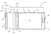
図1は、本発明のシステム構成全体を、液晶パネルを平面図にして示した図である。図2は、液晶パネル及びバックライトを提供するライトガイドの高さ方向の構造を示す側面図である。 FIG. 1 is a diagram showing the entire system configuration of the present invention in a plan view of a liquid crystal panel. FIG. 2 is a side view showing a structure in the height direction of a light guide that provides a liquid crystal panel and a backlight.
バックライト制御システム10は、液晶パネル20、その背面に配置されるライトガイド50、ライトガイド50に光を提供する光源装置30、及び光源装置30の制御装置40を含む。光源装置30からの出力光は、ライトガイド50へとその一側端51から導入される。図示しないが、ライトガイド50は液晶パネル20と略同じ幅寸法を有する。これにより、ライトガイド50は、液晶パネル20の背後から、少なくとも液晶パネル20の表示部21の全面にわたって白色或いは任意の色の光を供給する。
The
光源装置30は、複数の発光装置31のアレイを配置する発光部32、その後段に置かれる光混合部33、及びライトガイド50の一側端51に光学的に結合される光出力部34を有する。複数の発光装置31は、異なる波長の光を発光する発光ダイオード装置とされる。例えば、発光ダイオード装置として、赤(R)、緑(G)、青(B)の三つの異なる色(即ち、各色域の異なる波長)の光を発光する装置が用意される。これらの発光装置31は、例えば幅方向に、それらの発光色に一定の規則性に基づいた順番でアレイを成すように配列される。
The
光混合部(またはミキサ)33は、これらの異なる色又は波長の光を混合する機能を有する。例えば、赤、緑、青各色の発光装置による発光強度のバランスを後述の制御装置40を用いて適正化すれば、光混合部33による光の混合により、見かけ上白色となる光をライトガイド50に提供することができる。本実施形態では、光混合部33は直線的に図示されるが、鏡面等を用いて曲線的な光路を構成して、光を混合させることもできる。
The light mixing unit (or mixer) 33 has a function of mixing light of these different colors or wavelengths. For example, if the balance of the light emission intensity of the light emitting devices of red, green, and blue is optimized using the
制御装置40は、光源装置30における各発光装置31の発光強度を制御する機能を有する。即ち、制御装置40は、光源装置30にある各発光装置31の発光強度を、個別に若しくは各発光色又は発光波長の発光装置31毎に制御する機能を有する。制御のための信号は、ライン82を介して光源装置30に提供される。制御装置40による制御態様は、図示しない適当なユーザインタフェースによる外部から提供されることもできるが、後述のフィードバック機構により自動制御されることもできる。
The
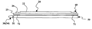
ライトガイド50に重ねて置かれる液晶パネル20は、液晶材料を封入するガラス板22、23を有する。底側板23は頂側板22よりも大面積とされ、中央に液晶表示面21が構成される。底側板23の一端側には、液晶駆動用のIC(又は駆動素子)24が配置される。本実施形態では、IC24は、底側板23の板面上にCOG実装される。ICが実装される側と光源装置30から光が導入される側は、液晶パネル20に対して共通の端側とされる。
The
IC24が実装される面と対向する底側の面には、遮光マスク72が形成される。遮光マスク72は、表示面21に対して不本意な光が進入するのを防止するためのもので、駆動回路の実装される位置の裏側の全面に遮光する手段を提供する。遮光マスク72は、例えば、樹脂製の遮光テープとされても良いし、他の場合には樹脂又は金属の層を底側板23の底面に部分的に印刷することによって形成しても良い。
A
液晶パネル20の表示面21を挟んでIC24の実装される側と対向する端側には、光センサ60が配置される。光センサ60は、バックライトの特性を安定化させるものであり、バックライトの一部をその各色又は波長ごとに検出する。検出された各色又は波長毎の強度信号は、ライン81を介して制御装置40に提供される。
An
制御装置40は、光センサ60での検出信号に基づいて、光源装置30における発光装置31の強度を変更する。例えば、白色のバックライトを提供する際に、発光色のうち一の成分の強度が経時変化によって相対的に小さくなったような場合に、その色を発光する発光装置31の発光強度を相対的に高めるようにして、安定した白色を維持させることができる。バックライトの色味の変化は、液晶表示装置の色再現性に直接影響を与えるので、上述の機能は極めて重要である。
The
本実施形態では、光センサ60は、底側板23上に前述の駆動素子24と同様にCOG実装される。光センサ60の実装される側と対向する底側の面には、駆動素子24の背面に置かれるのと同様の遮光マスク71が形成されるが、この遮光マスク71の内側には、ライトガイド50からの光の一部が光センサ60に達することができるように、窓73が形成される。即ち、光センサ60は、窓73を介して底側から底側板23に導入された光を受光してこれを検出する。従って、光センサ60は、その光感知部分が底側を向くようにして底側板23上に実装される。
In the present embodiment, the
本発明の好適実施形態となるバックライト制御システム10は、液晶パネル20、光源装置30、制御装置40が個別に製造され、それらをライン81、82等を含めて組立てることによって実現される。ここで、光センサ60の実装については、液晶パネル20の製造が完了し、他の装置と組立てられる際に行われても良いが、液晶パネル20の製造に際して、同じプロセスの中で行われても良い。後者は、プロセスの簡略化の点でのメリットを有する。なお、液晶パネル20の製造に際して、上述の遮光マスク71、72を形成する工程も行われる。
The
本実施形態の構成によれば、光センサ60を含めた全体寸法を厚さ方向に小さくできる。従って、この構成によれば、例えば携帯用の小型の装置への応用のために、ライトガイド50が比較的薄いことが要求されるような場合にも適用できるという利点を有する。
According to the configuration of the present embodiment, the overall dimensions including the
以上のように、本発明の好適実施形態となるバックライト制御システムについて詳細に説明したが、これはあくまでも例示的なものであり、本発明を制限するものではなく、当業者によって、さらに様々な変形・変更が可能である。 As described above, the backlight control system according to the preferred embodiment of the present invention has been described in detail. However, this is merely an example, and does not limit the present invention. Deformation / change is possible.
10 バックライト制御システム
20 液晶パネル
23 ガラス基板(底側板)
30 光源装置
31 発光装置
40 制御装置
50 ライトガイド
60 光センサ
10 Backlight control system
20 Liquid crystal panel 23 Glass substrate (bottom side plate)
30 light source device 31 light emitting
Claims (10)
前記光センサは、前記液晶パネルを構成する底側のガラス基板の頂面上に、前記液晶パネルを駆動する駆動素子とともに、該駆動素子が実装される端側と液晶表示面を挟んで逆側となる位置に実装され、前記ガラス基板の背面側から進入して該ガラス基板を通過した光を感知するようにされることを特徴とするバックライト制御システム。 A light source including a light emitting device that emits light of a plurality of different wavelengths controlled by a control device, a light guide that receives light from the light source and provides a backlight from the back of the liquid crystal panel, and a plurality of the backlights A backlight control system comprising: a photosensor for sensing components of different wavelengths; and means for feeding back a signal of the photosensor to the control device.
The optical sensor has a driving element for driving the liquid crystal panel on a top surface of a glass substrate on the bottom side constituting the liquid crystal panel, and an opposite side across the liquid crystal display surface with an end side where the driving element is mounted The backlight control system is mounted at a position such that the light enters the glass substrate from the back side and passes through the glass substrate.
前記光センサは、各波長の光を識別して別個に検出可能とされ、
前記制御装置は、前記複数の発光ダイオードの各々の発光を別個に制御する手段を備えることを特徴とする、請求項1に記載のバックライト制御システム。 The light source includes a plurality of light emitting diodes that emit light of different wavelengths of at least three colors as a light emitting device, and includes means for mixing light from the plurality of light emitting diodes,
The optical sensor is capable of identifying and separately detecting light of each wavelength,
The backlight control system according to claim 1, wherein the control device includes means for separately controlling light emission of each of the plurality of light emitting diodes.
前記光センサを配置する工程は、前記液晶パネルの前記ガラス基板上に前記光センサを実装する工程を含むことを特徴とするバックライト制御システムの製造方法。 A liquid crystal panel manufacturing process including a step of mounting a driving circuit for driving liquid crystal on a glass substrate, a step of arranging a light guide for providing a backlight on the back surface of the liquid crystal panel, and a light source optically connected to the light guide And a light sensor for detecting a part of the light serving as the backlight in the vicinity of the light guide so that a detection signal from the light sensor is fed back to the control circuit of the light source. In a method for manufacturing a backlight control system including a process,
The step of disposing the photosensor includes a step of mounting the photosensor on the glass substrate of the liquid crystal panel.
The manufacturing process of the liquid crystal panel includes a step of forming a light shielding mask on the back surface of the glass substrate facing the surface on which the photosensor is mounted, and forming a window for capturing a part of the light inside the light shielding mask. The manufacturing method of the backlight control system of Claim 8 characterized by the above-mentioned.
Priority Applications (3)
| Application Number | Priority Date | Filing Date | Title |
|---|---|---|---|
| JP2005057334A JP4589757B2 (en) | 2005-03-02 | 2005-03-02 | Backlight control system for small liquid crystal display, liquid crystal panel therefor, and method for manufacturing backlight control system |
| US11/364,729 US7742033B2 (en) | 2005-03-02 | 2006-02-28 | Backlight control system for small size display, LCD panel therefor, and method for making backlight control system |
| TW095106825A TWI335569B (en) | 2005-03-02 | 2006-03-01 | Backlight control system for small size display, lcd panel therefor and method of making backlight control system |
Applications Claiming Priority (1)
| Application Number | Priority Date | Filing Date | Title |
|---|---|---|---|
| JP2005057334A JP4589757B2 (en) | 2005-03-02 | 2005-03-02 | Backlight control system for small liquid crystal display, liquid crystal panel therefor, and method for manufacturing backlight control system |
Publications (2)
| Publication Number | Publication Date |
|---|---|
| JP2006243242A JP2006243242A (en) | 2006-09-14 |
| JP4589757B2 true JP4589757B2 (en) | 2010-12-01 |
Family
ID=37034780
Family Applications (1)
| Application Number | Title | Priority Date | Filing Date |
|---|---|---|---|
| JP2005057334A Expired - Fee Related JP4589757B2 (en) | 2005-03-02 | 2005-03-02 | Backlight control system for small liquid crystal display, liquid crystal panel therefor, and method for manufacturing backlight control system |
Country Status (3)
| Country | Link |
|---|---|
| US (1) | US7742033B2 (en) |
| JP (1) | JP4589757B2 (en) |
| TW (1) | TWI335569B (en) |
Families Citing this family (5)
| Publication number | Priority date | Publication date | Assignee | Title |
|---|---|---|---|---|
| JP4589757B2 (en) | 2005-03-02 | 2010-12-01 | アバゴ・テクノロジーズ・イーシービーユー・アイピー(シンガポール)プライベート・リミテッド | Backlight control system for small liquid crystal display, liquid crystal panel therefor, and method for manufacturing backlight control system |
| JP2008181109A (en) * | 2006-12-27 | 2008-08-07 | Semiconductor Energy Lab Co Ltd | Liquid crystal display device and electronic apparatus using the same |
| KR101380581B1 (en) | 2007-01-18 | 2014-04-01 | 삼성디스플레이 주식회사 | Liquid crystal display panel having power supply line and liquid crystal display |
| KR20090120252A (en) * | 2008-05-19 | 2009-11-24 | 삼성전자주식회사 | Display device |
| CN107464515A (en) * | 2017-07-17 | 2017-12-12 | 努比亚技术有限公司 | Screen brightness regulation method, mobile terminal and storage medium |
Family Cites Families (13)
| Publication number | Priority date | Publication date | Assignee | Title |
|---|---|---|---|---|
| JPS58170053A (en) | 1982-03-31 | 1983-10-06 | Semiconductor Energy Lab Co Ltd | Semiconductor device |
| JPH0876096A (en) | 1994-09-06 | 1996-03-22 | Casio Comput Co Ltd | Liquid crystal display temperature compensation method |
| KR0148053B1 (en) * | 1995-05-12 | 1998-09-15 | 김광호 | Apparatus and method for driving back light source of liquid crystal display device |
| JP2000081608A (en) * | 1998-06-29 | 2000-03-21 | Sanyo Electric Co Ltd | Liquid crystal display device with light condensing mechanism |
| US6127783A (en) | 1998-12-18 | 2000-10-03 | Philips Electronics North America Corp. | LED luminaire with electronically adjusted color balance |
| US6344641B1 (en) | 1999-08-11 | 2002-02-05 | Agilent Technologies, Inc. | System and method for on-chip calibration of illumination sources for an integrated circuit display |
| US6448550B1 (en) | 2000-04-27 | 2002-09-10 | Agilent Technologies, Inc. | Method and apparatus for measuring spectral content of LED light source and control thereof |
| JP3766042B2 (en) | 2002-06-21 | 2006-04-12 | 三菱電機株式会社 | Rear light source for display device and liquid crystal display device |
| JP3715616B2 (en) | 2002-11-20 | 2005-11-09 | Necディスプレイソリューションズ株式会社 | Liquid crystal display device and common voltage setting method of the device |
| JP4612406B2 (en) * | 2004-02-09 | 2011-01-12 | 株式会社日立製作所 | Liquid crystal display device |
| JP4353038B2 (en) * | 2004-09-22 | 2009-10-28 | セイコーエプソン株式会社 | Liquid crystal display device and electronic device |
| JP2006201221A (en) * | 2005-01-18 | 2006-08-03 | Seiko Epson Corp | Liquid crystal device and electronic device |
| JP4589757B2 (en) | 2005-03-02 | 2010-12-01 | アバゴ・テクノロジーズ・イーシービーユー・アイピー(シンガポール)プライベート・リミテッド | Backlight control system for small liquid crystal display, liquid crystal panel therefor, and method for manufacturing backlight control system |
-
2005
- 2005-03-02 JP JP2005057334A patent/JP4589757B2/en not_active Expired - Fee Related
-
2006
- 2006-02-28 US US11/364,729 patent/US7742033B2/en not_active Expired - Fee Related
- 2006-03-01 TW TW095106825A patent/TWI335569B/en not_active IP Right Cessation
Also Published As
| Publication number | Publication date |
|---|---|
| US7742033B2 (en) | 2010-06-22 |
| US20060215099A1 (en) | 2006-09-28 |
| TWI335569B (en) | 2011-01-01 |
| JP2006243242A (en) | 2006-09-14 |
| TW200643886A (en) | 2006-12-16 |
Similar Documents
| Publication | Publication Date | Title |
|---|---|---|
| US6964500B2 (en) | Planar light source device, liquid crystal display apparatus, and display apparatus | |
| EP3771942B1 (en) | Color conversion sheet, backlight unit, and display device | |
| US9746710B2 (en) | Quantum dot light source device, backlight module, and liquid crystal display device | |
| US7997784B2 (en) | Light guide apparatus of backlight module | |
| US8184239B2 (en) | Liquid crystal display device | |
| US7887206B2 (en) | Optical unit, backlight assembly with the optical unit, and display device with the backlight assembly | |
| US8643803B2 (en) | Liquid crystal display device | |
| US20110096265A1 (en) | Backlight unit and display device including the same | |
| CN104620040B (en) | Illuminator, display device and radiovisor | |
| CN101382255A (en) | Backlight unit and display device | |
| JP4589757B2 (en) | Backlight control system for small liquid crystal display, liquid crystal panel therefor, and method for manufacturing backlight control system | |
| US11231616B2 (en) | Color conversion sheet, backlight unit and display device | |
| CN108227295B (en) | Display device and method of manufacturing the same | |
| US11143912B2 (en) | Backlight unit and display device including the same | |
| KR101203520B1 (en) | Assembling structure of liquid crystal display | |
| US20210149230A1 (en) | Backlight unit and display device using the same | |
| US8143791B2 (en) | Control system for light-emitting device | |
| KR100877868B1 (en) | Backlight unit | |
| KR102564142B1 (en) | Back light unit and display device using the same | |
| KR101920760B1 (en) | Liquid crystal display module inculding backlight unit | |
| JP4622615B2 (en) | Electro-optical device and electronic apparatus | |
| KR102037849B1 (en) | Liquid Crystal Display Device | |
| KR20100052166A (en) | Liquid crystal display device | |
| US20120293725A1 (en) | Lighting device, display device and television receiver | |
| CN115116334A (en) | Backlight module and display device using the same |
Legal Events
| Date | Code | Title | Description |
|---|---|---|---|
| A711 | Notification of change in applicant |
Free format text: JAPANESE INTERMEDIATE CODE: A711 Effective date: 20070405 |
|
| A621 | Written request for application examination |
Free format text: JAPANESE INTERMEDIATE CODE: A621 Effective date: 20070530 |
|
| A977 | Report on retrieval |
Free format text: JAPANESE INTERMEDIATE CODE: A971007 Effective date: 20100823 |
|
| TRDD | Decision of grant or rejection written | ||
| A01 | Written decision to grant a patent or to grant a registration (utility model) |
Free format text: JAPANESE INTERMEDIATE CODE: A01 Effective date: 20100907 |
|
| A01 | Written decision to grant a patent or to grant a registration (utility model) |
Free format text: JAPANESE INTERMEDIATE CODE: A01 |
|
| A61 | First payment of annual fees (during grant procedure) |
Free format text: JAPANESE INTERMEDIATE CODE: A61 Effective date: 20100910 |
|
| R150 | Certificate of patent or registration of utility model |
Ref document number: 4589757 Country of ref document: JP Free format text: JAPANESE INTERMEDIATE CODE: R150 Free format text: JAPANESE INTERMEDIATE CODE: R150 |
|
| FPAY | Renewal fee payment (event date is renewal date of database) |
Free format text: PAYMENT UNTIL: 20130917 Year of fee payment: 3 |
|
| S111 | Request for change of ownership or part of ownership |
Free format text: JAPANESE INTERMEDIATE CODE: R313111 |
|
| R250 | Receipt of annual fees |
Free format text: JAPANESE INTERMEDIATE CODE: R250 |
|
| R350 | Written notification of registration of transfer |
Free format text: JAPANESE INTERMEDIATE CODE: R350 |
|
| R250 | Receipt of annual fees |
Free format text: JAPANESE INTERMEDIATE CODE: R250 |
|
| R250 | Receipt of annual fees |
Free format text: JAPANESE INTERMEDIATE CODE: R250 |
|
| R250 | Receipt of annual fees |
Free format text: JAPANESE INTERMEDIATE CODE: R250 |
|
| R250 | Receipt of annual fees |
Free format text: JAPANESE INTERMEDIATE CODE: R250 |
|
| R250 | Receipt of annual fees |
Free format text: JAPANESE INTERMEDIATE CODE: R250 |
|
| S111 | Request for change of ownership or part of ownership |
Free format text: JAPANESE INTERMEDIATE CODE: R313111 |
|
| R350 | Written notification of registration of transfer |
Free format text: JAPANESE INTERMEDIATE CODE: R350 |
|
| R250 | Receipt of annual fees |
Free format text: JAPANESE INTERMEDIATE CODE: R250 |
|
| LAPS | Cancellation because of no payment of annual fees |