EP1926136A2 - Electronic component and method for manufacturing the same - Google Patents
Electronic component and method for manufacturing the same Download PDFInfo
- Publication number
- EP1926136A2 EP1926136A2 EP07022679A EP07022679A EP1926136A2 EP 1926136 A2 EP1926136 A2 EP 1926136A2 EP 07022679 A EP07022679 A EP 07022679A EP 07022679 A EP07022679 A EP 07022679A EP 1926136 A2 EP1926136 A2 EP 1926136A2
- Authority
- EP
- European Patent Office
- Prior art keywords
- electronic component
- conductive material
- manufacturing
- electronic
- wiring boards
- Prior art date
- Legal status (The legal status is an assumption and is not a legal conclusion. Google has not performed a legal analysis and makes no representation as to the accuracy of the status listed.)
- Granted
Links
Images




Classifications
-
- H—ELECTRICITY
- H10—SEMICONDUCTOR DEVICES; ELECTRIC SOLID-STATE DEVICES NOT OTHERWISE PROVIDED FOR
- H10W—GENERIC PACKAGES, INTERCONNECTIONS, CONNECTORS OR OTHER CONSTRUCTIONAL DETAILS OF DEVICES COVERED BY CLASS H10
- H10W70/00—Package substrates; Interposers; Redistribution layers [RDL]
- H10W70/60—Insulating or insulated package substrates; Interposers; Redistribution layers
- H10W70/67—Insulating or insulated package substrates; Interposers; Redistribution layers characterised by their insulating layers or insulating parts
- H10W70/69—Insulating materials thereof
- H10W70/698—Semiconductor materials that are electrically insulating, e.g. undoped silicon
-
- H—ELECTRICITY
- H10—SEMICONDUCTOR DEVICES; ELECTRIC SOLID-STATE DEVICES NOT OTHERWISE PROVIDED FOR
- H10W—GENERIC PACKAGES, INTERCONNECTIONS, CONNECTORS OR OTHER CONSTRUCTIONAL DETAILS OF DEVICES COVERED BY CLASS H10
- H10W70/00—Package substrates; Interposers; Redistribution layers [RDL]
- H10W70/60—Insulating or insulated package substrates; Interposers; Redistribution layers
-
- H—ELECTRICITY
- H05—ELECTRIC TECHNIQUES NOT OTHERWISE PROVIDED FOR
- H05K—PRINTED CIRCUITS; CASINGS OR CONSTRUCTIONAL DETAILS OF ELECTRIC APPARATUS; MANUFACTURE OF ASSEMBLAGES OF ELECTRICAL COMPONENTS
- H05K3/00—Apparatus or processes for manufacturing printed circuits
- H05K3/30—Assembling printed circuits with electric components, e.g. with resistors
-
- H—ELECTRICITY
- H05—ELECTRIC TECHNIQUES NOT OTHERWISE PROVIDED FOR
- H05K—PRINTED CIRCUITS; CASINGS OR CONSTRUCTIONAL DETAILS OF ELECTRIC APPARATUS; MANUFACTURE OF ASSEMBLAGES OF ELECTRICAL COMPONENTS
- H05K3/00—Apparatus or processes for manufacturing printed circuits
- H05K3/46—Manufacturing multilayer circuits
- H05K3/4611—Manufacturing multilayer circuits by laminating two or more circuit boards
- H05K3/4614—Manufacturing multilayer circuits by laminating two or more circuit boards the electrical connections between the circuit boards being made during lamination
-
- H—ELECTRICITY
- H10—SEMICONDUCTOR DEVICES; ELECTRIC SOLID-STATE DEVICES NOT OTHERWISE PROVIDED FOR
- H10D—INORGANIC ELECTRIC SEMICONDUCTOR DEVICES
- H10D99/00—Subject matter not provided for in other groups of this subclass
-
- H—ELECTRICITY
- H10—SEMICONDUCTOR DEVICES; ELECTRIC SOLID-STATE DEVICES NOT OTHERWISE PROVIDED FOR
- H10W—GENERIC PACKAGES, INTERCONNECTIONS, CONNECTORS OR OTHER CONSTRUCTIONAL DETAILS OF DEVICES COVERED BY CLASS H10
- H10W70/00—Package substrates; Interposers; Redistribution layers [RDL]
- H10W70/01—Manufacture or treatment
- H10W70/05—Manufacture or treatment of insulating or insulated package substrates, or of interposers, or of redistribution layers
-
- H—ELECTRICITY
- H10—SEMICONDUCTOR DEVICES; ELECTRIC SOLID-STATE DEVICES NOT OTHERWISE PROVIDED FOR
- H10W—GENERIC PACKAGES, INTERCONNECTIONS, CONNECTORS OR OTHER CONSTRUCTIONAL DETAILS OF DEVICES COVERED BY CLASS H10
- H10W70/00—Package substrates; Interposers; Redistribution layers [RDL]
- H10W70/60—Insulating or insulated package substrates; Interposers; Redistribution layers
- H10W70/611—Insulating or insulated package substrates; Interposers; Redistribution layers for connecting multiple chips together
-
- H—ELECTRICITY
- H10—SEMICONDUCTOR DEVICES; ELECTRIC SOLID-STATE DEVICES NOT OTHERWISE PROVIDED FOR
- H10W—GENERIC PACKAGES, INTERCONNECTIONS, CONNECTORS OR OTHER CONSTRUCTIONAL DETAILS OF DEVICES COVERED BY CLASS H10
- H10W70/00—Package substrates; Interposers; Redistribution layers [RDL]
- H10W70/60—Insulating or insulated package substrates; Interposers; Redistribution layers
- H10W70/62—Insulating or insulated package substrates; Interposers; Redistribution layers characterised by their interconnections
- H10W70/63—Vias, e.g. via plugs
- H10W70/635—Through-vias
-
- H—ELECTRICITY
- H10—SEMICONDUCTOR DEVICES; ELECTRIC SOLID-STATE DEVICES NOT OTHERWISE PROVIDED FOR
- H10W—GENERIC PACKAGES, INTERCONNECTIONS, CONNECTORS OR OTHER CONSTRUCTIONAL DETAILS OF DEVICES COVERED BY CLASS H10
- H10W70/00—Package substrates; Interposers; Redistribution layers [RDL]
- H10W70/60—Insulating or insulated package substrates; Interposers; Redistribution layers
- H10W70/67—Insulating or insulated package substrates; Interposers; Redistribution layers characterised by their insulating layers or insulating parts
- H10W70/68—Shapes or dispositions thereof
-
- H—ELECTRICITY
- H10—SEMICONDUCTOR DEVICES; ELECTRIC SOLID-STATE DEVICES NOT OTHERWISE PROVIDED FOR
- H10W—GENERIC PACKAGES, INTERCONNECTIONS, CONNECTORS OR OTHER CONSTRUCTIONAL DETAILS OF DEVICES COVERED BY CLASS H10
- H10W70/00—Package substrates; Interposers; Redistribution layers [RDL]
- H10W70/60—Insulating or insulated package substrates; Interposers; Redistribution layers
- H10W70/67—Insulating or insulated package substrates; Interposers; Redistribution layers characterised by their insulating layers or insulating parts
- H10W70/68—Shapes or dispositions thereof
- H10W70/685—Shapes or dispositions thereof comprising multiple insulating layers
-
- H—ELECTRICITY
- H10—SEMICONDUCTOR DEVICES; ELECTRIC SOLID-STATE DEVICES NOT OTHERWISE PROVIDED FOR
- H10W—GENERIC PACKAGES, INTERCONNECTIONS, CONNECTORS OR OTHER CONSTRUCTIONAL DETAILS OF DEVICES COVERED BY CLASS H10
- H10W76/00—Containers; Fillings or auxiliary members therefor; Seals
- H10W76/10—Containers or parts thereof
-
- H—ELECTRICITY
- H10—SEMICONDUCTOR DEVICES; ELECTRIC SOLID-STATE DEVICES NOT OTHERWISE PROVIDED FOR
- H10W—GENERIC PACKAGES, INTERCONNECTIONS, CONNECTORS OR OTHER CONSTRUCTIONAL DETAILS OF DEVICES COVERED BY CLASS H10
- H10W90/00—Package configurations
-
- H—ELECTRICITY
- H10—SEMICONDUCTOR DEVICES; ELECTRIC SOLID-STATE DEVICES NOT OTHERWISE PROVIDED FOR
- H10W—GENERIC PACKAGES, INTERCONNECTIONS, CONNECTORS OR OTHER CONSTRUCTIONAL DETAILS OF DEVICES COVERED BY CLASS H10
- H10W90/00—Package configurations
- H10W90/401—Package configurations characterised by multiple insulating or insulated package substrates, interposers or RDLs
-
- H—ELECTRICITY
- H05—ELECTRIC TECHNIQUES NOT OTHERWISE PROVIDED FOR
- H05K—PRINTED CIRCUITS; CASINGS OR CONSTRUCTIONAL DETAILS OF ELECTRIC APPARATUS; MANUFACTURE OF ASSEMBLAGES OF ELECTRICAL COMPONENTS
- H05K2201/00—Indexing scheme relating to printed circuits covered by H05K1/00
- H05K2201/03—Conductive materials
- H05K2201/0332—Structure of the conductor
- H05K2201/0364—Conductor shape
- H05K2201/0367—Metallic bump or raised conductor not used as solder bump
-
- H—ELECTRICITY
- H05—ELECTRIC TECHNIQUES NOT OTHERWISE PROVIDED FOR
- H05K—PRINTED CIRCUITS; CASINGS OR CONSTRUCTIONAL DETAILS OF ELECTRIC APPARATUS; MANUFACTURE OF ASSEMBLAGES OF ELECTRICAL COMPONENTS
- H05K2201/00—Indexing scheme relating to printed circuits covered by H05K1/00
- H05K2201/09—Shape and layout
- H05K2201/09209—Shape and layout details of conductors
- H05K2201/095—Conductive through-holes or vias
- H05K2201/096—Vertically aligned vias, holes or stacked vias
-
- H—ELECTRICITY
- H05—ELECTRIC TECHNIQUES NOT OTHERWISE PROVIDED FOR
- H05K—PRINTED CIRCUITS; CASINGS OR CONSTRUCTIONAL DETAILS OF ELECTRIC APPARATUS; MANUFACTURE OF ASSEMBLAGES OF ELECTRICAL COMPONENTS
- H05K2203/00—Indexing scheme relating to apparatus or processes for manufacturing printed circuits covered by H05K3/00
- H05K2203/04—Soldering or other types of metallurgic bonding
- H05K2203/049—Wire bonding
-
- H—ELECTRICITY
- H05—ELECTRIC TECHNIQUES NOT OTHERWISE PROVIDED FOR
- H05K—PRINTED CIRCUITS; CASINGS OR CONSTRUCTIONAL DETAILS OF ELECTRIC APPARATUS; MANUFACTURE OF ASSEMBLAGES OF ELECTRICAL COMPONENTS
- H05K2203/00—Indexing scheme relating to apparatus or processes for manufacturing printed circuits covered by H05K3/00
- H05K2203/07—Treatments involving liquids, e.g. plating, rinsing
- H05K2203/0703—Plating
- H05K2203/0733—Method for plating stud vias, i.e. massive vias formed by plating the bottom of a hole without plating on the walls
-
- H—ELECTRICITY
- H05—ELECTRIC TECHNIQUES NOT OTHERWISE PROVIDED FOR
- H05K—PRINTED CIRCUITS; CASINGS OR CONSTRUCTIONAL DETAILS OF ELECTRIC APPARATUS; MANUFACTURE OF ASSEMBLAGES OF ELECTRICAL COMPONENTS
- H05K3/00—Apparatus or processes for manufacturing printed circuits
- H05K3/40—Forming printed elements for providing electric connections to or between printed circuits
- H05K3/4007—Surface contacts, e.g. bumps
- H05K3/4015—Surface contacts, e.g. bumps using auxiliary conductive elements, e.g. pieces of metal foil, metallic spheres
-
- H—ELECTRICITY
- H10—SEMICONDUCTOR DEVICES; ELECTRIC SOLID-STATE DEVICES NOT OTHERWISE PROVIDED FOR
- H10H—INORGANIC LIGHT-EMITTING SEMICONDUCTOR DEVICES HAVING POTENTIAL BARRIERS
- H10H20/00—Individual inorganic light-emitting semiconductor devices having potential barriers, e.g. light-emitting diodes [LED]
- H10H20/80—Constructional details
- H10H20/85—Packages
- H10H20/8506—Containers
-
- H—ELECTRICITY
- H10—SEMICONDUCTOR DEVICES; ELECTRIC SOLID-STATE DEVICES NOT OTHERWISE PROVIDED FOR
- H10W—GENERIC PACKAGES, INTERCONNECTIONS, CONNECTORS OR OTHER CONSTRUCTIONAL DETAILS OF DEVICES COVERED BY CLASS H10
- H10W72/00—Interconnections or connectors in packages
- H10W72/071—Connecting or disconnecting
- H10W72/072—Connecting or disconnecting of bump connectors
- H10W72/07251—Connecting or disconnecting of bump connectors characterised by changes in properties of the bump connectors during connecting
-
- H—ELECTRICITY
- H10—SEMICONDUCTOR DEVICES; ELECTRIC SOLID-STATE DEVICES NOT OTHERWISE PROVIDED FOR
- H10W—GENERIC PACKAGES, INTERCONNECTIONS, CONNECTORS OR OTHER CONSTRUCTIONAL DETAILS OF DEVICES COVERED BY CLASS H10
- H10W72/00—Interconnections or connectors in packages
- H10W72/20—Bump connectors, e.g. solder bumps or copper pillars; Dummy bumps; Thermal bumps
-
- H—ELECTRICITY
- H10—SEMICONDUCTOR DEVICES; ELECTRIC SOLID-STATE DEVICES NOT OTHERWISE PROVIDED FOR
- H10W—GENERIC PACKAGES, INTERCONNECTIONS, CONNECTORS OR OTHER CONSTRUCTIONAL DETAILS OF DEVICES COVERED BY CLASS H10
- H10W90/00—Package configurations
- H10W90/701—Package configurations characterised by the relative positions of pads or connectors relative to package parts
- H10W90/721—Package configurations characterised by the relative positions of pads or connectors relative to package parts of bump connectors
- H10W90/724—Package configurations characterised by the relative positions of pads or connectors relative to package parts of bump connectors between a chip and a stacked insulating package substrate, interposer or RDL
-
- Y—GENERAL TAGGING OF NEW TECHNOLOGICAL DEVELOPMENTS; GENERAL TAGGING OF CROSS-SECTIONAL TECHNOLOGIES SPANNING OVER SEVERAL SECTIONS OF THE IPC; TECHNICAL SUBJECTS COVERED BY FORMER USPC CROSS-REFERENCE ART COLLECTIONS [XRACs] AND DIGESTS
- Y10—TECHNICAL SUBJECTS COVERED BY FORMER USPC
- Y10T—TECHNICAL SUBJECTS COVERED BY FORMER US CLASSIFICATION
- Y10T29/00—Metal working
- Y10T29/49—Method of mechanical manufacture
- Y10T29/49002—Electrical device making
- Y10T29/49117—Conductor or circuit manufacturing
- Y10T29/49124—On flat or curved insulated base, e.g., printed circuit, etc.
- Y10T29/49155—Manufacturing circuit on or in base
Definitions
- the present disclosure relates to an electronic component using a semiconductor substrate, as well as to a method for manufacturing the same.
- a semiconductor element such as silicon
- a substrate used for mounting electronic elements such as semiconductor elements, in lieu of a ceramic material or a resin material.
- An interposer which is formed from; e.g., silicon and which is used for mounting electronic elements exhibits superior thermal conductivity than those exhibited by the ceramic material and the resin material. For this reason, when an electronic element to be mounted generates heat, such an interposer has the advantage of exhibiting superior heat dissipation.
- a substrate formed from a semiconductor material is more easily precision-fabricated compared with the ceramic material and the resin material, and has an advantage at the time of formation of microstructures.
- an interposer formed from a semiconductor material such as silicon
- JP-A-2000-39371 Japanese Patent Unexamined Document: JP-A-2000-39371 .
- a specific challenge to be met by the present invention is to provide a highly-reliable electronic component which is formed from a semiconductor substrate and which has a multilayer structure and a method for manufacturing the component.
- an electronic component including:
- the present invention provides a highly-reliable electronic component, which is formed from a semiconductor substrate and has a multilayer structure, and a method for manufacturing the component.
- a method of manufacturing an electronic component includes the steps of:
- an electronic component having a multilayer structure can be readily fabricated by means of bonding the plurality of semiconductor substrates and electrically interconnecting the conductive material buried in the through holes of the plurality of semiconductor substrates. Therefore, related-art complicated processes employed when a multilayer structure is formed in a semiconductor substrate are not required, and the electronic component can be manufactured by way of simple manufacturing processes. Consequently, the cost of manufacture of an electronic component is reduced, and the reliability of an electronic component to be fabricated becomes enhanced.
- bonding the plurality of wiring boards facilitates sealing of an electronic element into a predetermined space (e.g., a cavity formed in the wiring board).
- a predetermined space e.g., a cavity formed in the wiring board.
- an electronic element can be easily sealed by forming a substrate from a semiconductor material; for example, silicon, and bonding a plurality of substrates.
- the above manufacturing method is characterized by the ability to essentially simultaneously perform 1) bonding of wiring boards, 2) electrical connection of a conductive material (wiring, via plugs, and the like), and 3) sealing of an electronic element to be mounted. Therefore, an electronic component in which an electronic component is sealed and which has a multilayer structure can be readily manufactured.
- Figs. 1 A through 1J are views showing a method for manufacturing an electronic component of a first exemplary embodiment and the configuration of an electronic component manufactured under the manufacturing method.
- a mask pattern 102 having openings 102A is formed over a semiconductor substrate 101 (e.g., a silicon wafer) made of; e.g., silicon.
- the mask pattern 102 can be formed by bonding; for example, a film-like resist (a dry film resist) or by patterning a resist layer which is formed by application of liquid resist coating through development and exposure by means of photolithography.
- the semiconductor substrate 101 is subjected to pattern etching (RIE: Reactive Ion Etching) while the mask pattern 102 serves as a mask.
- RIE Reactive Ion Etching
- through holes (via holes) 101A penetrating through the semiconductor substrate 101 are formed.
- the mask pattern 102 is removed (exfoliated) after etching.
- the conductive material (the via plug) 104 is formed, the essential requirement is to perform processing provided below.
- a seed layer (a feeding layer) is formed on the insulation film 103 by means of electroless deposition, and a mask pattern is formed on the seed layer.
- the conductive material 104 is formed by means of electrolytic plating. The mask pattern and excessive areas of the seed layer which will be exposed as a result of removal of the mask pattern are removed. Thus, a wiring board 100 shown in Fig. 1D is formed.
- the wiring board 100 is additionally provided with a structure which facilitates electrical connection of the wiring board 100.
- metal layers 105 and 106 made of Ni-Au (a multilayer structure including an Au layer and an Ni layer, wherein the Au layer is positioned on an outer side) for facilitating electrical connection are formed on both ends of each conductive material 104.
- the metal layer 105 formed on a surface of the conductive material 104 to which another wiring board is to be bonded in a subsequent step is preferably formed so as not to protrude from the through hole; for example, in such a way that the surface of the metal layer 105 becomes substantially flush with the surface of the semiconductor substrate 101 (the insulation film 103).
- the metal layer 106 formed on the lower end of the conductive material 104 opposite to its upper end is formed so as to extend from the conductive material layer 104 toward the insulation film 103 located outside of the conductive material 104, to thus enable easy formation of an external connection terminal; for example, a solder bump.
- a projection (which will be sometimes called an electrical connection member or a bump) formed from a bonding wire made of; e.g., Au, is formed on the metal layer 105 by use of; for example, a wire bonding apparatus.
- the projections 107 are formed by means of continuous connection of the bonding wire to the metal layers 105 and disconnection of the bonding wire. Therefore, the projection 107 is formed in a convex shape (the shape of a projection) upwardly from a bonded portion.
- a wiring board to be bonded to the wiring board 100 is formed.
- a mask pattern 202 having openings 202A is formed, in the same manner as in the step shown in Fig. 1A, over a semiconductor substrate (e.g., a silicon wafer) 201 made of; e.g., silicon.
- the mask pattern 202 can be formed by bonding; for example, a film-like resist (a dry film resist) or by patterning a resist layer which is formed by coating liquid resist through development and exposure by means of photolithography.
- through holes (via holes) 201A, an insulation film 203, and a conductive film 204 are formed on the semiconductor substrate 201 in the same manner as in the previously-described processes shown in Figs. 1B to 1D.
- the through holes 201 A, the insulation film 203, and the conductive material 204 shown in the drawing can be formed in the same manner as are the through holes 101A, the insulation film 103, and the conductive material 104 in the processes shown in Figs. 1B to 1D.
- a wiring board 200 shown in the drawing can be formed.
- the side (i.e., the lower end in the drawing) of the conductive material 204 that is to be connected to the projection 107 in a subsequent step is preferably formed so as to become recessed in the through hole 201 by a predetermined amount (a height H).
- a height H a predetermined amount
- metal layers 205 and 206 formed from Ni-Au are formed on both ends of the conductive material 204 in order to facilitate electrical connection.
- the metal layer 206 provided on the side (the lower end in the drawing) of the conductive material 204 to which another wiring board is bonded in a subsequent step is formed in a position recessed in the through hole by a predetermined amount.
- the metal layer 205 formed on the upper end of the conductive material 204 opposite to its lower end is formed so as to extend from the conductive material 204 toward the insulation film 203 located outside of the conductive material 204, to thus enable easy formation of an external connection terminal; for example, a solder bump.
- the insulation films 103 and 203 are made of a silicon oxide film
- these films can be bonded together by means of pressing and heating with good adhesive force.
- the insulation films 103 and 203 may also be bonded together while the insulation films 103 and 203 in bonding surface of the films are removed, to thus make silicon exposed.
- the two wiring boards can be bonded together with superior adhesion force by means of pressurization and heating.
- the insulation film of any one of the wiring board 100 and the wiring board 200 may also be removed, to thus bring silicon in contact with the silicon oxide film, and these may also be bonded together by means of anodic bonding.
- the projection (the electrical connection member) 107 sandwiched between the conductive material 104 (the metal layer 105) and the conductive material 204 (the metal layer 206) becomes flat by pressurization and heating, to thus be bonded to the metal layer 206. Consequently, the conductive material 104 and the conductive material 204 are electrically connected together through the projection 107.
- various electronic elements e.g., semiconductor elements and the like
- the metal layer 106 can be electrically connected to an object of connection, such as a mother board, by use of solder bumps.
- the electronic component 400 can be used as an interposer which is formed by employing a semiconductor substrate and which has a multilayer structure.
- the plurality of semiconductor substrates (silicon substrates) 100 and 200 are bonded together, and the conductive materials 104 and 204 formed on the respective wiring boards 100 and 200 are electrically connected together by means of the projection conductive material 107, so that an electronic component having a multilayer structure can be fabricated readily.
- the method for forming a multilayer structure is made simpler in terms of processes. Hence, the cost of manufacture of an electronic component can be curtailed. Moreover, since the manufacturing processes become simple, the reliability of a manufactured electronic component is enhanced.
- the semiconductor material for example, silicon
- the semiconductor material exhibits superior thermal conductivity when compared with that exhibited by a ceramic material or a resin material
- the semiconductor material has the advantage of effecting superior heat dissipation when a mounted electronic element has generated heat.
- the semiconductor material is suitable for a case where a high-performance electronic element generating large amounts of heat is mounted.
- the substrate is easier to precision-fabricate the substrate than a ceramic material or a resin material and a minute structure is easily formed.
- the substrate is suitable for a case where a miniaturized high-performance electronic element is mounted.
- a new mask pattern 303 is formed on the semiconductor substrate 301.
- the mask pattern 303 can be formed in the same manner that the mask pattern 302 is formed. Further, the mask pattern 303 is formed so as to be provided with openings 303A and 303B.
- the opening 303B corresponds to a recess portion (cavity) which will be formed in a subsequent step and where an electronic element is mounted.
- the semiconductor substrate 301 is subjected to pattern etching (RIE) while the mask pattern 303 serves as a mask.
- RIE pattern etching
- a recess (cavity) 301C of a predetermined depth is formed in the semiconductor substrate 301.
- the through holes 301B penetrate through a bottom portion (the semiconductor substrate 301) of the recess 301C.
- the mask pattern 303 is exfoliated.
- an insulation film 304 formed from (for example, a silicon oxide film) is formed on the surface of the semiconductor substrate 301 including an interior wall surface of the recess 301C.
- the conductive materials (via plugs) 305 and 306 are formed as follows:
- a seed layer (a feeding layer) is formed on the insulation film 304 by means of electroless plating, and a mask pattern is formed on the seed layer.
- the conductive materials via plugs) 305 and 306 are formed by means of electrolytic plating. Further, the mask pattern and excessive areas of the seed layer exposed as a result of removal of the mask pattern are removed.
- a wiring board 300 shown in Fig. 2F can be formed.
- the wiring board 300 is additionally provided with a structure which facilitates electrical connection of the wiring board 300, and an electronic element is further mounted thereon.
- metal layers 307 and 308 made of Ni-Au are formed on both ends of the conductive material 305 in order to facilitate electrical connection.
- the metal layer 308 formed on the lower end of the conductive material 305 opposite to its upper end is formed so as to extend from the conductive material 305 toward the insulation film 304 located outside of the conductive material 305, to thus enable easy formation of an external connection terminal such as a solder bump.
- a metal layer 309 is formed also on the lower end of the conductive material 306 as in the case of the lower end of the conductive material 305.
- projections (sometimes called electrical connection members or bumps) 310 and 311 formed from a bonding wire (Au) are formed on the metal layer 307 and the conductive material 306, by use of the wire bonding apparatus.
- the projections 310 and 311 are formed by continuous connection of a bonding wire and disconnection of the bonding wire.
- the wiring board 300 and the wiring board 200 shown in Fig. 1H of the first exemplary embodiment are positioned so that the projection 310 and the metal layer 206 correspond to each other, and the wiring boards are bonded together by pressing (pressurization) and heating.
- the insulation films 304 and 203 are formed from a silicon oxide film, these films can be bonded to each other with good adhesion force by means of pressurization and heating. Further, the wiring board 300 and the wiring board 200 may also be bonded to each other with silicon being exposed, by removing the insulation films 304 and 203 in bonding areas thereof. Even in this case, the two wiring boards can be bonded together with superior adhesion force by means of pressurization and heating. Further, the insulation film of any one of the wiring board 300 and the wiring board 200 may also be removed, to thus bring silicon in contact with the silicon oxide film, and these may also be bonded together by means of anodic bonding.
- the projection (the electrical connection member) 310 located between the conductive material 305 (the metal layer 307) and the conductive material 204 (the metal layer 206) is subjected to pressurization and heating, to thus become flat and connected to the metal layer 206. Consequently, the conductive material 305 and the conductive material 204 are electrically connected together through the projection 310.
- the electronic element 312 mounted in the recess 301C of the semiconductor substrate 301 is sealed (enclosed) in the recess 301C as a result of bonding the wiring board 300 (the semiconductor substrate 301) and the wiring board 200 (the semiconductor substrate 201) together.
- the electronic component 500 shown in Fig. 2K can be thus manufactured.
- the electronic component 500 shown in Fig. 2K is structured such that the wiring board 300 having a structure in which the conductive material 305 is buried in through holes penetrating through the semiconductor substrate 301 is bonded to the wiring board 200 having a structure in which the conductive material 204 is buried in through holes penetrating through the semiconductor substrate 201. Further, by means of the projection (the electrical connection member) 310 which is pressed by means of the above bonding, the electronic component has a structure of the conductive material (the via plug) 305 and the conductive material (the via plug) 204 being electrically connected together.
- the method for manufacturing an electronic component facilitates sealing of an electronic element in a predetermined space (e.g., a recess formed in a wiring board) by means of bonding a plurality of wiring boards.
- the manufacturing method is characterized by substantially simultaneously performing, in the step shown in Fig. 2J, 1) bonding of the wiring board 300 and the wiring board 200 (the semiconductor substrate 301 and the semiconductor substrate 201), 2) electrical connection of the conductive materials 305 and 204 of the respective wiring boards 300 and 200, and 3) sealing of an electronic element 311 to be mounted.
- the openings 501 serve as opening sections for allowing entrance of light into the optical-functional element (the electronic element 312) or exit of light from the optical-functional element.
- the openings 501 are used for allowing entrance of light into a light-receiving element.
- the openings 501 are used for allowing exit of light from the light-emitting element.
- an optically-transparent cover may also be provided on each of the opening sections 501.
- an electronic element 502 is mounted on a surface opposite to the surface of the wiring board 200 (the semiconductor substrate 201) facing the recess 301C, wherein the wiring board 200 is bonded to the wiring board 300 having the recess 301C formed therein.
- Fig. 4 is a view showing an electronic component 500B of a fourth exemplary embodiment.
- the electronic component 500B of the present embodiment differs from the electronic component 500A of the third exemplary embodiment in the following points.
- a plurality of electronic elements to be mounted in a recess 301C i.e., electronic elements 312A and 312B.
- a plurality of openings (openings 501 A and 501 B) penetrating through the semiconductor substrate 201 (the wiring board 200) are formed in correspondence to the electronic elements.
- the opening 501A is used for allowing exit of light from the light-emitting element.
- the opening section 501B is used for allowing entrance of light to the light-receiving element.
- the electronic component 500B of the present embodiment is provided with an electronic element 503.
- the number of electronic elements mounted on the wiring board 200 is not limited to one, and the electronic elements may also be in numbers.
- the electronic component 500C of the present embodiment is characterized in that a device (e.g., a Zener diode) 504 having a plurality of dopant diffusion areas of different concentrations or conductivity types is fabricated in the semiconductor substrate 201 (the wiring board 200).
- a device e.g., a Zener diode 504 having a plurality of dopant diffusion areas of different concentrations or conductivity types is fabricated in the semiconductor substrate 201 (the wiring board 200).
- the present embodiment enables miniaturization and weight-reduction of an electronic component.
- the present invention it is possible to provide a highly-reliable electronic component which is formed by use of a semiconductor substrate and which has a multilayer structure and a method for manufacturing the component.
Landscapes
- Engineering & Computer Science (AREA)
- Manufacturing & Machinery (AREA)
- Microelectronics & Electronic Packaging (AREA)
- Production Of Multi-Layered Print Wiring Board (AREA)
- Internal Circuitry In Semiconductor Integrated Circuit Devices (AREA)
- Combinations Of Printed Boards (AREA)
- Printing Elements For Providing Electric Connections Between Printed Circuits (AREA)
Abstract

Description
- This application is based on and claims priority from
Japanese Patent Application No. 2006-316202 - The present disclosure relates to an electronic component using a semiconductor substrate, as well as to a method for manufacturing the same.
- A semiconductor element, such as silicon, is used for; for example, a substrate (interposer) used for mounting electronic elements such as semiconductor elements, in lieu of a ceramic material or a resin material. An interposer which is formed from; e.g., silicon and which is used for mounting electronic elements exhibits superior thermal conductivity than those exhibited by the ceramic material and the resin material. For this reason, when an electronic element to be mounted generates heat, such an interposer has the advantage of exhibiting superior heat dissipation.
- Further, a substrate formed from a semiconductor material is more easily precision-fabricated compared with the ceramic material and the resin material, and has an advantage at the time of formation of microstructures. For these reasons, there are cases where an interposer formed from a semiconductor material, such as silicon, is adopted for an especially-miniaturized electronic component. (see e.g., Japanese Patent Unexamined Document:
JP-A-2000-39371 - However, particularly for the purpose of forming complicate wiring (a conductive material) for use in mounting elements in the case of formation of an interposer built from a semiconductor substrate, there arises a problem that processes for manufacturing the interposer become more complicated than a case where an interposer built from a related-art resin material is formed.
- For instance, when a multilayer structure into which wiring (the conductive material) for use in mounting elements is stacked into layers is formed from a semiconductor substrate, processes for forming the wiring (the conductive material) become more complicated when compared with those employed in the case where a resin material is used.
- When the processes for manufacturing an interposer are complicated as mentioned above, manufacturing cost increases, and a concern about an increase in manufacturing cost and there arises a decrease in reliability of wiring of an interposer to be formed.
- Specifically, the above practical problems arise in the case where a structure in which wiring (a conductive material) of an interposer enabling mounting of electronic elements or having electronic elements mounted thereon is stacked into layers is formed using a semiconductor substrate.
- In light of the above, a method of manufacturing an electronic component according to independent claim 1, and an electronic component according to independent claim 7 are provided.
Further advantages, features, aspects and details are evident from the dependent claims, the description and the drawings.
Exemplary embodiments of the present invention provide a novel and useful electronic component and a method for manufacturing the same, which solve the above-described problems - A specific challenge to be met by the present invention is to provide a highly-reliable electronic component which is formed from a semiconductor substrate and which has a multilayer structure and a method for manufacturing the component.
- According to a first aspect of the present invention, the above-described problems are solved by a method of manufacturing an electronic component, including the steps of:
- a) forming a plurality of wiring boards that include first through holes penetrating through a semiconductor substrate and conductive material buried in the first through holes;
- b) providing conductive projections on the conductive material of any of the plurality of wiring boards; and
- c) bonding the plurality of wiring boards to each other and electrically connecting the conductive material of the respective wiring boards by the projections.
- Further, according to a second aspect of the present invention, the above-described problems are solved by an electronic component including:
- a plurality of wiring boards that are provided with through holes penetrating through a semiconductor substrate, the through holes being filled with conductive material; and
- electrical connection members provided on any of the conductive material of the plurality of wiring boards, wherein
- the plurality of wiring boards are bonded to each other, and
- the conductive material of the respective wiring boards are electrically connected to each other by the electrical connection members which are pressed by bonding of the plurality of wiring boards.
- The present invention provides a highly-reliable electronic component, which is formed from a semiconductor substrate and has a multilayer structure, and a method for manufacturing the component.
- The invention will be better understood by reference to the following description of embodiments of the invention taken in conjunction with the accompanying drawings, wherein:
- Fig. 1A is a view showing a method for manufacturing an electronic component of a first exemplary embodiment (part 1);
- Fig. 1 B is a view showing the method for manufacturing an electronic component of the first exemplary embodiment (part 2);
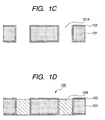
- Fig. 1C is a view showing the method for manufacturing an electronic component of the first exemplary embodiment (part 3);
- Fig. 1D is a view showing the method for manufacturing an electronic component of the first exemplary embodiment (part 4);
- Fig. 1E is a view showing the method for manufacturing an electronic component of the first exemplary embodiment (part 5);
- Fig. 1F is a view showing the method for manufacturing an electronic component of the first exemplary embodiment (part 6);
- Fig. 1 G is a view showing the method for manufacturing an electronic component of the first exemplary embodiment (part 7);
- Fig. 1H is a view showing the method for manufacturing an electronic component of the first exemplary embodiment (part 8);
- Fig. 1 I is a view showing the method for manufacturing an electronic component of the first exemplary embodiment (part 9);
- Fig. 1 J is a view showing the method for manufacturing an electronic component of the first exemplary embodiment (part 10);
- Fig. 2A is a view showing a method for manufacturing an electronic component of a second exemplary embodiment (part 1);
- Fig. 2B is a view showing the method for manufacturing an electronic component of the second exemplary embodiment (part 2);
- Fig. 2C is a view showing the method for manufacturing an electronic component of the second exemplary embodiment (part 3);
- Fig. 2D is a view showing the method for manufacturing an electronic component of the second exemplary embodiment (part 4);
- Fig. 2E is a view showing the method for manufacturing an electronic component of the second exemplary embodiment (part 5);
- Fig. 2F is a view showing the method for manufacturing an electronic component of the second exemplary embodiment (part 6);
- Fig. 2G is a view showing the method for manufacturing an electronic component of the second exemplary embodiment (part 7);
- Fig. 2H is a view showing the method for manufacturing an electronic component of the second exemplary embodiment (part 8);
- Fig. 2I is a view showing the method for manufacturing an electronic component of the second exemplary embodiment (part 9);
- Fig. 2J is a view showing the method for manufacturing an electronic component of the second exemplary embodiment (part 10);
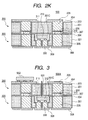
- Fig. 2K is a view showing the method for manufacturing an electronic component of the second exemplary embodiment (part 11);
- Fig. 3 is a view showing an electronic component of a third exemplary embodiment;
- Fig. 4 is a view showing an electronic component of a fourth exemplary embodiment; and
- Fig. 5 is a view showing an electronic component of a fifth exemplary embodiment.
- According to the present invention, a method of manufacturing an electronic component includes the steps of:
- a) forming a plurality of wiring boards that include first through holes penetrating through a semiconductor substrate and conductive material buried in the first through holes;
- b) providing conductive projections on any of the conductive material of the plurality of wiring boards; and
- c) bonding the plurality of wiring boards to each other and electrically connecting the conductive material of the respective wiring boards by the projections.
- Namely, according to the above manufacturing method, an electronic component having a multilayer structure can be readily fabricated by means of bonding the plurality of semiconductor substrates and electrically interconnecting the conductive material buried in the through holes of the plurality of semiconductor substrates. Therefore, related-art complicated processes employed when a multilayer structure is formed in a semiconductor substrate are not required, and the electronic component can be manufactured by way of simple manufacturing processes. Consequently, the cost of manufacture of an electronic component is reduced, and the reliability of an electronic component to be fabricated becomes enhanced.
- Further, according to the above manufacturing method, bonding the plurality of wiring boards facilitates sealing of an electronic element into a predetermined space (e.g., a cavity formed in the wiring board). For instance, in the case of a related-art substrate formed from a resin material, it is difficult to seal (enclose) an element to be mounted while preventing intrusion of oxygen, a moisture content, and the like.
- In the meantime, according to the manufacturing method, an electronic element can be easily sealed by forming a substrate from a semiconductor material; for example, silicon, and bonding a plurality of substrates.
- Namely, the above manufacturing method is characterized by the ability to essentially simultaneously perform 1) bonding of wiring boards, 2) electrical connection of a conductive material (wiring, via plugs, and the like), and 3) sealing of an electronic element to be mounted. Therefore, an electronic component in which an electronic component is sealed and which has a multilayer structure can be readily manufactured.
- The manufacturing method and the configuration of an electronic component fabricated thereby will now be described by reference to the drawings.
- Figs. 1 A through 1J are views showing a method for manufacturing an electronic component of a first exemplary embodiment and the configuration of an electronic component manufactured under the manufacturing method.
- In relation to the drawings provided below, there are occasions where the previously-described elements are assigned with the same reference numerals and where their repeated explanations are omitted (the same also applies to embodiments provided below).
- First, in a process shown in Fig. 1A, a
mask pattern 102 havingopenings 102A is formed over a semiconductor substrate 101 (e.g., a silicon wafer) made of; e.g., silicon. Themask pattern 102 can be formed by bonding; for example, a film-like resist (a dry film resist) or by patterning a resist layer which is formed by application of liquid resist coating through development and exposure by means of photolithography. - In a process shown in Fig. 1B, the
semiconductor substrate 101 is subjected to pattern etching (RIE: Reactive Ion Etching) while themask pattern 102 serves as a mask. By means of etching, through holes (via holes) 101A penetrating through thesemiconductor substrate 101 are formed. Themask pattern 102 is removed (exfoliated) after etching. - In a step shown in Fig. 1C, an
insulation film 103 made of; e.g. a silicon oxide film, is formed on the surface of thesemiconductor substrate 101 including interior wall surfaces of the throughholes 101 A. - In a step shown in Fig. 1D, a conductive material (a via plug) 104 formed from; e.g., Cu, is buried in the through
holes 101A. When the conductive material (the via plug) 104 is formed, the essential requirement is to perform processing provided below. - First, a seed layer (a feeding layer) is formed on the
insulation film 103 by means of electroless deposition, and a mask pattern is formed on the seed layer. Subsequently, theconductive material 104 is formed by means of electrolytic plating. The mask pattern and excessive areas of the seed layer which will be exposed as a result of removal of the mask pattern are removed. Thus, awiring board 100 shown in Fig. 1D is formed. - In following steps, the
wiring board 100 is additionally provided with a structure which facilitates electrical connection of thewiring board 100. - In a step shown in Fig. 1E,
metal layers conductive material 104. - In this case, the
metal layer 105 formed on a surface of theconductive material 104 to which another wiring board is to be bonded in a subsequent step is preferably formed so as not to protrude from the through hole; for example, in such a way that the surface of themetal layer 105 becomes substantially flush with the surface of the semiconductor substrate 101 (the insulation film 103). - Further, the
metal layer 106 formed on the lower end of theconductive material 104 opposite to its upper end is formed so as to extend from theconductive material layer 104 toward theinsulation film 103 located outside of theconductive material 104, to thus enable easy formation of an external connection terminal; for example, a solder bump. - Moreover, a projection (which will be sometimes called an electrical connection member or a bump) formed from a bonding wire made of; e.g., Au, is formed on the
metal layer 105 by use of; for example, a wire bonding apparatus. Theprojections 107 are formed by means of continuous connection of the bonding wire to the metal layers 105 and disconnection of the bonding wire. Therefore, theprojection 107 is formed in a convex shape (the shape of a projection) upwardly from a bonded portion. - In a step shown in Fig. 1F and subsequent steps, a wiring board to be bonded to the
wiring board 100 is formed. - In a step shown in Fig. 1F, a
mask pattern 202 havingopenings 202A is formed, in the same manner as in the step shown in Fig. 1A, over a semiconductor substrate (e.g., a silicon wafer) 201 made of; e.g., silicon. Themask pattern 202 can be formed by bonding; for example, a film-like resist (a dry film resist) or by patterning a resist layer which is formed by coating liquid resist through development and exposure by means of photolithography. - In a step shown in Fig. 1G, through holes (via holes) 201A, an
insulation film 203, and aconductive film 204 are formed on thesemiconductor substrate 201 in the same manner as in the previously-described processes shown in Figs. 1B to 1D. The throughholes 201 A, theinsulation film 203, and theconductive material 204 shown in the drawing can be formed in the same manner as are the throughholes 101A, theinsulation film 103, and theconductive material 104 in the processes shown in Figs. 1B to 1D. Thus, awiring board 200 shown in the drawing can be formed. - In the case shown in the drawing, the side (i.e., the lower end in the drawing) of the
conductive material 204 that is to be connected to theprojection 107 in a subsequent step is preferably formed so as to become recessed in the throughhole 201 by a predetermined amount (a height H). The reason for this is that, when thewiring board 100 and thewiring board 200 are bonded to each other, providing a space where theprojections 107 are present (pressed) is ensured. - Next, in a step shown in Fig. 1H,
metal layers conductive material 204 in order to facilitate electrical connection. - In this case, the
metal layer 206 provided on the side (the lower end in the drawing) of theconductive material 204 to which another wiring board is bonded in a subsequent step is formed in a position recessed in the through hole by a predetermined amount. Moreover, themetal layer 205 formed on the upper end of theconductive material 204 opposite to its lower end is formed so as to extend from theconductive material 204 toward theinsulation film 203 located outside of theconductive material 204, to thus enable easy formation of an external connection terminal; for example, a solder bump. - In a step shown in Fig. 1I, the
wiring board 100 and thewiring board 200 are bonded together by means of pressing (pressurization) and heating after being positioned in such a way that theprojections 107 correspond to themetal layer 206. - For example, when the
insulation films insulation films insulation films wiring board 100 and thewiring board 200 may also be removed, to thus bring silicon in contact with the silicon oxide film, and these may also be bonded together by means of anodic bonding. - In this process, the projection (the electrical connection member) 107 sandwiched between the conductive material 104 (the metal layer 105) and the conductive material 204 (the metal layer 206) becomes flat by pressurization and heating, to thus be bonded to the
metal layer 206. Consequently, theconductive material 104 and theconductive material 204 are electrically connected together through theprojection 107. - As mentioned above, an
electronic component 400 shown in Fig. 1 J can be manufactured. Theelectronic component 400 shown in Fig. 1J is structured such that thewiring board 100 having a structure in which theconductive material 104 is buried in the through holes penetrating through thesemiconductor substrate 101 is bonded to thewiring board 200 having a structure in which theconductive material 204 is buried in the through holes penetrating through the semiconductor. By means of the projections (the electrical connection sections) 107 which are pressed by means of the above bonding, the conductive material (the via plugs) 104 and the conductive material (the via plugs) 204 are electrically connected to each other. - For example, various electronic elements (e.g., semiconductor elements and the like) are mounted on the
metal layer 205, and themetal layer 106 can be electrically connected to an object of connection, such as a mother board, by use of solder bumps. Namely, theelectronic component 400 can be used as an interposer which is formed by employing a semiconductor substrate and which has a multilayer structure. - According to the method for manufacturing an electronic component, the plurality of semiconductor substrates (silicon substrates) 100 and 200 are bonded together, and the
conductive materials respective wiring boards conductive material 107, so that an electronic component having a multilayer structure can be fabricated readily. - Specifically, when compared with a related-art method, the method for forming a multilayer structure is made simpler in terms of processes. Hence, the cost of manufacture of an electronic component can be curtailed. Moreover, since the manufacturing processes become simple, the reliability of a manufactured electronic component is enhanced.
- Moreover, since the semiconductor material (for example, silicon) exhibits superior thermal conductivity when compared with that exhibited by a ceramic material or a resin material, the semiconductor material has the advantage of effecting superior heat dissipation when a mounted electronic element has generated heat. In short, the semiconductor material is suitable for a case where a high-performance electronic element generating large amounts of heat is mounted.
- According to a characteristic of a substrate formed from a semiconductor substrate, it is easier to precision-fabricate the substrate than a ceramic material or a resin material and a minute structure is easily formed. Specifically, the substrate is suitable for a case where a miniaturized high-performance electronic element is mounted.
- According to the manufacturing method of the present invention, sealing an electronic element in a predetermined space (e.g. a recess formed in a wiring board) is facilitated by means of bonding a plurality of wiring boards. An embodiment, i.e. a second exemplary embodiment, where an electronic element is sealed in a predetermined space will now be described.
- First, in a step shown in Fig. 2A, a
mask pattern 302 havingopenings mask pattern 302 can be formed, for example, by bonding a film-like resist (a dry film resist) or by patterning a resist layer which is formed by coating liquid resist through development and exposure by means of photolithography. - In a step shown in Fig. 2B, a
semiconductor substrate 301 is subjected to pattern etching (RIE) while themask pattern 302 serves as a mask. Through holes (via holes) 301A and 301B penetrating through thesemiconductor substrate 301 are formed by means of etching. Further, the throughhole 301B is a through hole for mounting an element, and it is used in forming a via plug to which an electronic element mounted in a subsequent step is connected. - After removal (exfoliation) of the
mask pattern 302 in a step shown in Fig. 2C, anew mask pattern 303 is formed on thesemiconductor substrate 301. Themask pattern 303 can be formed in the same manner that themask pattern 302 is formed. Further, themask pattern 303 is formed so as to be provided withopenings opening 303B corresponds to a recess portion (cavity) which will be formed in a subsequent step and where an electronic element is mounted. - Next, in a step shown in Fig. 2D, the
semiconductor substrate 301 is subjected to pattern etching (RIE) while themask pattern 303 serves as a mask. A recess (cavity) 301C of a predetermined depth is formed in thesemiconductor substrate 301. The throughholes 301B penetrate through a bottom portion (the semiconductor substrate 301) of therecess 301C. After the above etching, themask pattern 303 is exfoliated. - Next, in a step shown in Fig. 2E, an
insulation film 304 formed from (for example, a silicon oxide film) is formed on the surface of thesemiconductor substrate 301 including an interior wall surface of therecess 301C. - Next, in a step shown in Fig. 2F, a
conductive material 305 made of; e.g., Cu, is buried in the throughhole 301A, and aconductive material 306 made of; e.g., Cu, is buried in the throughhole 301B. The conductive materials (via plugs) 305 and 306 are formed as follows: - First, a seed layer (a feeding layer) is formed on the
insulation film 304 by means of electroless plating, and a mask pattern is formed on the seed layer. Subsequently, the conductive materials (via plugs) 305 and 306 are formed by means of electrolytic plating. Further, the mask pattern and excessive areas of the seed layer exposed as a result of removal of the mask pattern are removed. Thus, awiring board 300 shown in Fig. 2F can be formed. - In subsequent steps, the
wiring board 300 is additionally provided with a structure which facilitates electrical connection of thewiring board 300, and an electronic element is further mounted thereon. - In a step shown in Fig. 2G,
metal layers conductive material 305 in order to facilitate electrical connection. - In this case, the
metal layer 105 formed on the side (the upper end in the drawing) of theconductive material 305 to which another wiring board is bonded in a subsequent step is formed so as not to protrude from the through hole. For example, it is preferable that the surface of themetal layer 307 becomes substantially flush with the surface of the semiconductor substrate 301 (the insulation film 304). - Moreover, the
metal layer 308 formed on the lower end of theconductive material 305 opposite to its upper end is formed so as to extend from theconductive material 305 toward theinsulation film 304 located outside of theconductive material 305, to thus enable easy formation of an external connection terminal such as a solder bump. Further, ametal layer 309 is formed also on the lower end of theconductive material 306 as in the case of the lower end of theconductive material 305. - Next, projections (sometimes called electrical connection members or bumps) 310 and 311 formed from a bonding wire (Au) are formed on the
metal layer 307 and theconductive material 306, by use of the wire bonding apparatus. As in the case of theprojections 107 of the first exemplary embodiment, theprojections - Next, in a step shown in Fig. 2I, an electronic element (e.g., a semiconductor element) 312 is mounted in a recess (cavity) 301C. The
electronic element 312 is electrically connected to theconductive material 306 through theprojection 311. - In a step shown in Fig. 2J, the
wiring board 300 and thewiring board 200 shown in Fig. 1H of the first exemplary embodiment are positioned so that theprojection 310 and themetal layer 206 correspond to each other, and the wiring boards are bonded together by pressing (pressurization) and heating. - When the
insulation films wiring board 300 and thewiring board 200 may also be bonded to each other with silicon being exposed, by removing theinsulation films wiring board 300 and thewiring board 200 may also be removed, to thus bring silicon in contact with the silicon oxide film, and these may also be bonded together by means of anodic bonding. - In this process, the projection (the electrical connection member) 310 located between the conductive material 305 (the metal layer 307) and the conductive material 204 (the metal layer 206) is subjected to pressurization and heating, to thus become flat and connected to the
metal layer 206. Consequently, theconductive material 305 and theconductive material 204 are electrically connected together through theprojection 310. - Further, in this step, the
electronic element 312 mounted in therecess 301C of thesemiconductor substrate 301 is sealed (enclosed) in therecess 301C as a result of bonding the wiring board 300 (the semiconductor substrate 301) and the wiring board 200 (the semiconductor substrate 201) together. - An
electronic component 500 shown in Fig. 2K can be thus manufactured. Theelectronic component 500 shown in Fig. 2K is structured such that thewiring board 300 having a structure in which theconductive material 305 is buried in through holes penetrating through thesemiconductor substrate 301 is bonded to thewiring board 200 having a structure in which theconductive material 204 is buried in through holes penetrating through thesemiconductor substrate 201. Further, by means of the projection (the electrical connection member) 310 which is pressed by means of the above bonding, the electronic component has a structure of the conductive material (the via plug) 305 and the conductive material (the via plug) 204 being electrically connected together. - The
electronic element 500 of the present embodiment is characterized in that theelectronic element 311 is sealed in therecess 301C of thewiring board 300. - According to the above-described manufacturing method, in addition to yielding the same characteristics and advantages as those described in connection with the first exemplary embodiment, the method for manufacturing an electronic component facilitates sealing of an electronic element in a predetermined space (e.g., a recess formed in a wiring board) by means of bonding a plurality of wiring boards.
- Namely, the manufacturing method is characterized by substantially simultaneously performing, in the step shown in Fig. 2J, 1) bonding of the
wiring board 300 and the wiring board 200 (thesemiconductor substrate 301 and the semiconductor substrate 201), 2) electrical connection of theconductive materials respective wiring boards electronic element 311 to be mounted. - Therefore, an electronic component in which an electronic element is sealed and which has a multilayer structure can be manufactured readily.
- For example, in the case of a substrate made of a related-art resin material, it is difficult to seal (enclose) an element to be mounted with avoiding from intrusion of oxygen or a moisture.
- In the meantime, according to the above-described manufacturing method, sealing of an electronic element, which is preferably used in a sealed manner, is facilitated by using a semiconductor material (e.g., silicon). And then, the electronic element is typified by an MEMS (Micro Electro Mechanical Systems) element and an optical-functional element (a light-emitting element or a light-receiving element).
- Further, for example, the manufacturing method (or the electronic component) of the present embodiment can be modified or altered as follows.
- Fig. 3 is a view showing an
electronic component 500A of a third exemplary embodiment. By reference to Fig. 3, theelectronic component 500A of the present embodiment differs from theelectronic component 500 of the second exemplary embodiment in following points. - First, in the present embodiment,
openings 501 penetrating through thesemiconductor substrate 201 are formed in the semiconductor substrate 201 (the wiring board 200). - For example, when the
electronic element 312 is an optical-functional element, theopenings 501 serve as opening sections for allowing entrance of light into the optical-functional element (the electronic element 312) or exit of light from the optical-functional element. Namely, when theelectronic element 312 is a light-receiving element, theopenings 501 are used for allowing entrance of light into a light-receiving element. When theelectronic element 312 is a light-emitting element, theopenings 501 are used for allowing exit of light from the light-emitting element. - In the steps shown in Figs. 1F and 1G of the first exemplary embodiment, it is required to form the
openings 501 simultaneously with formation of the throughholes 201 A. In order to seal theelectronic element 312, an optically-transparent cover may also be provided on each of the openingsections 501. - In the
electronic component 500A of the present embodiment, anelectronic element 502 is mounted on a surface opposite to the surface of the wiring board 200 (the semiconductor substrate 201) facing therecess 301C, wherein thewiring board 200 is bonded to thewiring board 300 having therecess 301C formed therein. - As mentioned above, the electronic component of the present invention can mount not only an electronic element to be sealed but also various other electronic elements. For instance, when the
electronic element 312 is an MEMS element, a drive element of the MEMS element can be mounted as in the case of the electronic element 512. - Fig. 4 is a view showing an
electronic component 500B of a fourth exemplary embodiment. By reference to Fig. 4, theelectronic component 500B of the present embodiment differs from theelectronic component 500A of the third exemplary embodiment in the following points. - First, in the present embodiment, there are a plurality of electronic elements to be mounted in a
recess 301C (i.e.,electronic elements openings electronic element 312A is a light-emitting element, theopening 501A is used for allowing exit of light from the light-emitting element. Moreover, when theelectronic element 312B is a light-receiving element, theopening section 501B is used for allowing entrance of light to the light-receiving element. As mentioned above, the plurality of electronic elements, such as a light-emitting element and a light-receiving element, may also be mounted on an electronic component. Further, when there are a plurality of light-emitting elements to be mounted, a plurality of openings may also be formed in correspondence to the elements in the wiring board. - In addition to the previously-descried
electronic element 502, theelectronic component 500B of the present embodiment is provided with anelectronic element 503. As mentioned above, the number of electronic elements mounted on thewiring board 200 is not limited to one, and the electronic elements may also be in numbers. - Fig. 5 is a view showing an
electronic component 500C of a fifth exemplary embodiment. By reference to Fig. 5, theelectronic component 500C of the present embodiment differs from theelectronic component 500A of the third exemplary embodiment in the following points. - The
electronic component 500C of the present embodiment is characterized in that a device (e.g., a Zener diode) 504 having a plurality of dopant diffusion areas of different concentrations or conductivity types is fabricated in the semiconductor substrate 201 (the wiring board 200). - Namely, the
electronic component 500C of the present embodiment is characterized in that a predetermined device (a diode, or the like) is fabricated by use of a semiconductor material (silicon) constituting a semiconductor substrate on which electronic elements are mounted. The device is used with being connected with electronic elements to be mounted on the semiconductor substrate. - Therefore, in the
electronic device 500C of the present embodiment, the number of elements to be surface-mounted is reduced. Specifically, the present embodiment enables miniaturization and weight-reduction of an electronic component. - In the present embodiments, the number of semiconductor substrates to be bonded together is not limited to two. An electronic element having a larger number of layers may also be configured by means of bonding three or more semiconductor substrates. Furthermore, the semiconductor substrate used in the above manufacturing method (or the electronic component) is not limited to a silicon substrate, and another semiconductor substrate (e.g. , SiGe or the like) may also be used.
- According to the present invention, it is possible to provide a highly-reliable electronic component which is formed by use of a semiconductor substrate and which has a multilayer structure and a method for manufacturing the component.
- While there has been described in connection with the exemplary embodiments of the present invention, it will be obvious to those skilled in the art that various changes and modification may be made therein without departing from the present invention. It is aimed, therefore, to cover in the appended claim all such changes and modifications as fall within the true spirit and scope of the present invention.
Claims (10)
- A method of manufacturing an electronic component (400; 500; 500A-C), comprising the steps of:a) forming a plurality of wiring boards (100, 200; 300) that include first through holes (101A, 201A; 301A) penetrating through a semiconductor substrate (101, 201; 301) and conductive material (104, 204; 305) buried in the first through holes;b) providing conductive projections (107; 310) on the conductive material of any of the plurality of wiring boards; andc) bonding the plurality of wiring boards to each other and electrically connecting the conductive material of the respective wiring boards by the projections.
- The method for manufacturing an electronic component according to Claim 1, wherein
the projections are formed from a bonding wire. - The method for manufacturing an electronic component according to any of Claims 1 to 2, wherein
in the step c), the projections are depressed so that the conductive material of the respective wiring boards are electrically connected to each other. - The method for manufacturing an electronic component according to any of Claims 1 to 3, further comprising:d) forming a recess portion (301C) for mounting an electronic element (312) in any of the plurality of semiconductor substrates;e) mounting the electronic element on the recess portionwherein
in the step c), the electronic element is sealed in the recess portion as a result of the plurality of semiconductor substrates being bonded together. - The method for manufacturing an electronic component according to Claim 4, wherein, in the step a), a second through hole (301B) for mounting an element is formed in a bottom of the recess along with the first through holes, and the conductive material (306) is buried in the second through hole, and
the electronic element is connected to the conductive material buried in the second through hole and the electronic element is mounted. - The method for manufacturing an electronic component according to any of Claims 4 to 5, wherein
the electronic element is an optical-functional element, and
in the step a), an opening (501; 501A, 501B) used for entrance/exit of light into/from the optical-functional element is formed in any of the plurality of semiconductor substrates. - An electronic component (400; 500; 500A-C) comprising:a plurality of wiring boards (100, 200; 300) that are provided with through holes (101A, 201A; 301A) penetrating through a semiconductor substrate, the through holes being filled with conductive material (104, 204; 305); andelectrical connection members (107; 310) provided on any of the conductive material of the plurality of wiring boards, whereinthe plurality of wiring boards are bonded to each other, andthe conductive material of the respective wiring boards are electrically connected to each other by the electrical connection members which are pressed by bonding of the plurality of wiring boards.
- The electronic component according to claim 7, wherein
an electronic element (312) is mounted in a recess portion formed in any of the plurality of semiconductor substrates, and
the electronic element is sealed in the recess by bonding the plurality of semiconductor substrates. - The electronic component according to claim 8, wherein
the electronic element is an optical-functional element, and
an opening (501; 501A, 501B) used for entrance/exit of light into/from the optical-functional element is formed in any of the plurality of wiring boards. - The electronic component according to any of claims 8 to 9, wherein
another electronic element (502) is mounted on a surface of the wiring board opposite to its surface facing the recess, the wiring board being bonded to the wiring board including the recess formed therein.
Applications Claiming Priority (1)
| Application Number | Priority Date | Filing Date | Title |
|---|---|---|---|
| JP2006316202A JP5064768B2 (en) | 2006-11-22 | 2006-11-22 | Electronic component and method for manufacturing electronic component |
Publications (3)
| Publication Number | Publication Date |
|---|---|
| EP1926136A2 true EP1926136A2 (en) | 2008-05-28 |
| EP1926136A3 EP1926136A3 (en) | 2008-10-29 |
| EP1926136B1 EP1926136B1 (en) | 2017-01-11 |
Family
ID=39185720
Family Applications (1)
| Application Number | Title | Priority Date | Filing Date |
|---|---|---|---|
| EP07022679.0A Active EP1926136B1 (en) | 2006-11-22 | 2007-11-22 | Electronic component and method for manufacturing the same |
Country Status (5)
| Country | Link |
|---|---|
| US (1) | US7894201B2 (en) |
| EP (1) | EP1926136B1 (en) |
| JP (1) | JP5064768B2 (en) |
| KR (1) | KR101436034B1 (en) |
| TW (1) | TWI442529B (en) |
Families Citing this family (19)
| Publication number | Priority date | Publication date | Assignee | Title |
|---|---|---|---|---|
| US8072079B2 (en) * | 2008-03-27 | 2011-12-06 | Stats Chippac, Ltd. | Through hole vias at saw streets including protrusions or recesses for interconnection |
| US11302617B2 (en) * | 2008-09-06 | 2022-04-12 | Broadpak Corporation | Scalable semiconductor interposer integration |
| US8664750B2 (en) * | 2008-11-17 | 2014-03-04 | Advanpack Solutions Pte. Ltd. | Semiconductor substrate, package and device |
| JP5568169B2 (en) * | 2009-02-23 | 2014-08-06 | 新光電気工業株式会社 | Wiring board and manufacturing method thereof |
| JP5367616B2 (en) | 2009-02-23 | 2013-12-11 | 新光電気工業株式会社 | Wiring board and manufacturing method thereof |
| US8804368B2 (en) * | 2009-04-30 | 2014-08-12 | Sony Corporation | Downward-facing optical component module |
| TWI430422B (en) * | 2009-09-01 | 2014-03-11 | 國立大學法人東北大學 | Wiring connection method and function device |
| US20110175218A1 (en) | 2010-01-18 | 2011-07-21 | Shiann-Ming Liou | Package assembly having a semiconductor substrate |
| US20110186960A1 (en) * | 2010-02-03 | 2011-08-04 | Albert Wu | Techniques and configurations for recessed semiconductor substrates |
| US8847376B2 (en) | 2010-07-23 | 2014-09-30 | Tessera, Inc. | Microelectronic elements with post-assembly planarization |
| JP2012049298A (en) * | 2010-08-26 | 2012-03-08 | Tohoku Univ | Device using porous metal for electrical connection and wiring connection method |
| US9029689B2 (en) * | 2010-12-23 | 2015-05-12 | Sunpower Corporation | Method for connecting solar cells |
| DE102012107668A1 (en) | 2012-08-21 | 2014-03-20 | Epcos Ag | component assembly |
| EP3104410B1 (en) * | 2014-03-10 | 2022-12-07 | Mitsubishi Heavy Industries, Ltd. | Multi-chip module, on-board computer, sensor interface substrate, and multi-chip module manufacturing method |
| US9481572B2 (en) | 2014-07-17 | 2016-11-01 | Texas Instruments Incorporated | Optical electronic device and method of fabrication |
| FR3042064B1 (en) * | 2015-10-05 | 2019-06-14 | Commissariat A L'energie Atomique Et Aux Energies Alternatives | DEVICE FOR CONNECTING AT LEAST ONE NANO-OBJECT ASSOCIATED WITH A CHIP ENABLING A CONNECTION TO AT LEAST ONE EXTERNAL ELECTRICAL SYSTEM AND ITS IMPLEMENTATION METHOD |
| US11600432B2 (en) | 2016-02-24 | 2023-03-07 | Murata Manufacturing Co., Ltd. | Substrate-embedded transformer with improved isolation |
| US11355427B2 (en) * | 2016-07-01 | 2022-06-07 | Intel Corporation | Device, method and system for providing recessed interconnect structures of a substrate |
| EP3483921B1 (en) * | 2017-11-11 | 2026-01-07 | AT & S Austria Technologie & Systemtechnik Aktiengesellschaft | Embedding known-good component in known-good cavity of known-good component carrier material with pre-formed electric connection structure |
Citations (2)
| Publication number | Priority date | Publication date | Assignee | Title |
|---|---|---|---|---|
| JP2000039371A (en) | 1998-07-21 | 2000-02-08 | Denso Corp | Semiconductor pressure sensor and method of manufacturing the same |
| JP2006316202A (en) | 2005-05-13 | 2006-11-24 | Takashi Sawaguchi | Terminal reactive oligomer having terminal vinylidene group |
Family Cites Families (14)
| Publication number | Priority date | Publication date | Assignee | Title |
|---|---|---|---|---|
| US5061987A (en) * | 1990-01-09 | 1991-10-29 | Northrop Corporation | Silicon substrate multichip assembly |
| JP2940269B2 (en) | 1990-12-26 | 1999-08-25 | 日本電気株式会社 | Connecting method of integrated circuit element |
| JP2001135785A (en) * | 1999-11-08 | 2001-05-18 | Seiko Epson Corp | Semiconductor chip, multi-chip package, semiconductor device, and electronic device, and manufacturing method thereof |
| DE10163799B4 (en) * | 2000-12-28 | 2006-11-23 | Matsushita Electric Works, Ltd., Kadoma | Semiconductor chip mounting substrate and method of manufacturing such a mounting substrate |
| JP2002290030A (en) * | 2001-03-23 | 2002-10-04 | Ngk Spark Plug Co Ltd | Wiring board |
| US6873529B2 (en) * | 2002-02-26 | 2005-03-29 | Kyocera Corporation | High frequency module |
| US7485489B2 (en) * | 2002-06-19 | 2009-02-03 | Bjoersell Sten | Electronics circuit manufacture |
| JP3908147B2 (en) * | 2002-10-28 | 2007-04-25 | シャープ株式会社 | Multilayer semiconductor device and manufacturing method thereof |
| US7361593B2 (en) * | 2002-12-17 | 2008-04-22 | Finisar Corporation | Methods of forming vias in multilayer substrates |
| JP2004273690A (en) * | 2003-03-07 | 2004-09-30 | Stanley Electric Co Ltd | Minimal light source LED element and method of manufacturing the same |
| JP2004363351A (en) * | 2003-06-05 | 2004-12-24 | Mitsubishi Electric Corp | Stacked semiconductor device |
| JP4312631B2 (en) * | 2004-03-03 | 2009-08-12 | 三菱電機株式会社 | Wafer level package structure and manufacturing method thereof, and device divided from wafer level package structure |
| JP4354398B2 (en) * | 2004-12-27 | 2009-10-28 | 三菱重工業株式会社 | Semiconductor device and manufacturing method thereof |
| US7262622B2 (en) * | 2005-03-24 | 2007-08-28 | Memsic, Inc. | Wafer-level package for integrated circuits |
-
2006
- 2006-11-22 JP JP2006316202A patent/JP5064768B2/en active Active
-
2007
- 2007-10-31 KR KR1020070109932A patent/KR101436034B1/en active Active
- 2007-11-20 US US11/943,194 patent/US7894201B2/en active Active
- 2007-11-20 TW TW096143839A patent/TWI442529B/en active
- 2007-11-22 EP EP07022679.0A patent/EP1926136B1/en active Active
Patent Citations (2)
| Publication number | Priority date | Publication date | Assignee | Title |
|---|---|---|---|---|
| JP2000039371A (en) | 1998-07-21 | 2000-02-08 | Denso Corp | Semiconductor pressure sensor and method of manufacturing the same |
| JP2006316202A (en) | 2005-05-13 | 2006-11-24 | Takashi Sawaguchi | Terminal reactive oligomer having terminal vinylidene group |
Also Published As
| Publication number | Publication date |
|---|---|
| TW200828545A (en) | 2008-07-01 |
| US20080117607A1 (en) | 2008-05-22 |
| EP1926136B1 (en) | 2017-01-11 |
| TWI442529B (en) | 2014-06-21 |
| EP1926136A3 (en) | 2008-10-29 |
| US7894201B2 (en) | 2011-02-22 |
| KR20080046558A (en) | 2008-05-27 |
| JP5064768B2 (en) | 2012-10-31 |
| KR101436034B1 (en) | 2014-09-01 |
| JP2008130934A (en) | 2008-06-05 |
Similar Documents
| Publication | Publication Date | Title |
|---|---|---|
| EP1926136B1 (en) | Electronic component and method for manufacturing the same | |
| US9865548B2 (en) | Polymer member based interconnect | |
| US8344492B2 (en) | Semiconductor device and method of manufacturing the same, and electronic apparatus | |
| US8859912B2 (en) | Coreless package substrate and fabrication method thereof | |
| US8669653B2 (en) | Semiconductor device having electronic component in through part, electronic device, and manufacturing method of semiconductor | |
| CN109003963B (en) | Semiconductor packaging and methods of manufacturing same | |
| US8294253B2 (en) | Semiconductor device, electronic device and method of manufacturing semiconductor device, having electronic component, sealing resin and multilayer wiring structure | |
| US20120049366A1 (en) | Package structure having through-silicon-via (tsv) chip embedded therein and fabrication method thereof | |
| US10002825B2 (en) | Method of fabricating package structure with an embedded electronic component | |
| EP1898462A2 (en) | Semiconductor apparatus | |
| CN102119588A (en) | Method for manufacturing module with built-in component, and module with built-in component | |
| CN101515574A (en) | Chip package carrier, chip package and manufacturing method thereof | |
| US8334590B1 (en) | Semiconductor device having insulating and interconnection layers | |
| JPWO2009041159A1 (en) | Device mounting substrate and manufacturing method thereof, circuit device and manufacturing method thereof, portable device | |
| TWI624011B (en) | Package structure and its manufacturing method | |
| KR100923542B1 (en) | Embedded Semiconductor Package Device Using Release Material and Its Manufacturing Method | |
| US7772689B2 (en) | Semiconductor package with a conductive post and wiring pattern | |
| US20040256715A1 (en) | Wiring board, semiconductor device and process of fabricating wiring board | |
| KR20170124769A (en) | Electric component module and manufacturing method threrof | |
| US20110216514A1 (en) | Combined multilayer circuit board having embedded components and manufacturing method of the same | |
| KR101582548B1 (en) | Method for manufacturing interposer and method for manufacturing semiconductor package using the same | |
| CN217883966U (en) | Component carrier comprising at least two components | |
| KR101579434B1 (en) | Method for manufacturing led package | |
| CN100441069C (en) | Electronic component mounting and mounting method | |
| CN119108357A (en) | Packaging structure, packaging method and electronic device |
Legal Events
| Date | Code | Title | Description |
|---|---|---|---|
| PUAI | Public reference made under article 153(3) epc to a published international application that has entered the european phase |
Free format text: ORIGINAL CODE: 0009012 |
|
| AK | Designated contracting states |
Kind code of ref document: A2 Designated state(s): AT BE BG CH CY CZ DE DK EE ES FI FR GB GR HU IE IS IT LI LT LU LV MC MT NL PL PT RO SE SI SK TR |
|
| AX | Request for extension of the european patent |
Extension state: AL BA HR MK RS |
|
| PUAL | Search report despatched |
Free format text: ORIGINAL CODE: 0009013 |
|
| AK | Designated contracting states |
Kind code of ref document: A3 Designated state(s): AT BE BG CH CY CZ DE DK EE ES FI FR GB GR HU IE IS IT LI LT LU LV MC MT NL PL PT RO SE SI SK TR |
|
| AX | Request for extension of the european patent |
Extension state: AL BA HR MK RS |
|
| RIC1 | Information provided on ipc code assigned before grant |
Ipc: H01L 21/48 20060101AFI20080325BHEP Ipc: H01L 23/538 20060101ALI20080919BHEP Ipc: H01L 23/14 20060101ALI20080919BHEP Ipc: H01L 23/498 20060101ALI20080919BHEP Ipc: H01L 25/16 20060101ALI20080919BHEP Ipc: H01L 23/13 20060101ALN20080325BHEP |
|
| 17P | Request for examination filed |
Effective date: 20090427 |
|
| AKX | Designation fees paid |
Designated state(s): DE |
|
| 17Q | First examination report despatched |
Effective date: 20150820 |
|
| REG | Reference to a national code |
Ref country code: DE Ref legal event code: R079 Ref document number: 602007049474 Country of ref document: DE Free format text: PREVIOUS MAIN CLASS: H01L0021480000 Ipc: H01L0023020000 |
|
| GRAP | Despatch of communication of intention to grant a patent |
Free format text: ORIGINAL CODE: EPIDOSNIGR1 |
|
| RIC1 | Information provided on ipc code assigned before grant |
Ipc: H05K 3/46 20060101ALI20160531BHEP Ipc: H01L 23/02 20060101AFI20160531BHEP Ipc: H01L 21/48 20060101ALI20160531BHEP Ipc: H05K 3/40 20060101ALI20160531BHEP Ipc: H01L 23/13 20060101ALI20160531BHEP Ipc: H01L 25/16 20060101ALI20160531BHEP Ipc: H01L 23/538 20060101ALI20160531BHEP Ipc: H01L 23/14 20060101ALI20160531BHEP Ipc: H01L 23/498 20060101ALI20160531BHEP Ipc: H01L 25/00 20060101ALI20160531BHEP Ipc: H01L 33/48 20100101ALI20160531BHEP |
|
| INTG | Intention to grant announced |
Effective date: 20160615 |
|
| GRAS | Grant fee paid |
Free format text: ORIGINAL CODE: EPIDOSNIGR3 |
|
| GRAA | (expected) grant |
Free format text: ORIGINAL CODE: 0009210 |
|
| AK | Designated contracting states |
Kind code of ref document: B1 Designated state(s): DE |
|
| REG | Reference to a national code |
Ref country code: DE Ref legal event code: R096 Ref document number: 602007049474 Country of ref document: DE |
|
| REG | Reference to a national code |
Ref country code: DE Ref legal event code: R097 Ref document number: 602007049474 Country of ref document: DE |
|
| PLBE | No opposition filed within time limit |
Free format text: ORIGINAL CODE: 0009261 |
|
| STAA | Information on the status of an ep patent application or granted ep patent |
Free format text: STATUS: NO OPPOSITION FILED WITHIN TIME LIMIT |
|
| 26N | No opposition filed |
Effective date: 20171012 |
|
| PGFP | Annual fee paid to national office [announced via postgrant information from national office to epo] |
Ref country code: DE Payment date: 20241001 Year of fee payment: 18 |
|
| REG | Reference to a national code |
Ref country code: DE Ref legal event code: R079 Ref document number: 602007049474 Country of ref document: DE Free format text: PREVIOUS MAIN CLASS: H01L0023020000 Ipc: H10W0076100000 |