EP1923918A2 - Graded hybrid amorphous silicon nanowire solar cells - Google Patents
Graded hybrid amorphous silicon nanowire solar cells Download PDFInfo
- Publication number
- EP1923918A2 EP1923918A2 EP07120384A EP07120384A EP1923918A2 EP 1923918 A2 EP1923918 A2 EP 1923918A2 EP 07120384 A EP07120384 A EP 07120384A EP 07120384 A EP07120384 A EP 07120384A EP 1923918 A2 EP1923918 A2 EP 1923918A2
- Authority
- EP
- European Patent Office
- Prior art keywords
- amorphous layer
- layer
- graded
- nanostructures
- doping
- Prior art date
- Legal status (The legal status is an assumption and is not a legal conclusion. Google has not performed a legal analysis and makes no representation as to the accuracy of the status listed.)
- Withdrawn
Links
- 239000002070 nanowire Substances 0.000 title description 36
- 229910021417 amorphous silicon Inorganic materials 0.000 title description 13
- 239000002086 nanomaterial Substances 0.000 claims abstract description 68
- 239000004065 semiconductor Substances 0.000 claims abstract description 58
- 238000000034 method Methods 0.000 claims abstract description 25
- 239000000758 substrate Substances 0.000 claims description 47
- 239000002019 doping agent Substances 0.000 claims description 21
- 239000000203 mixture Substances 0.000 claims description 17
- 238000000151 deposition Methods 0.000 claims description 13
- 238000004519 manufacturing process Methods 0.000 claims description 13
- 239000002243 precursor Substances 0.000 claims description 13
- 230000001965 increasing effect Effects 0.000 claims description 10
- 239000004020 conductor Substances 0.000 claims description 9
- 230000008021 deposition Effects 0.000 claims description 6
- 238000000623 plasma-assisted chemical vapour deposition Methods 0.000 claims description 5
- 238000004050 hot filament vapor deposition Methods 0.000 claims description 4
- 238000004544 sputter deposition Methods 0.000 claims description 3
- 239000012780 transparent material Substances 0.000 claims description 3
- 238000002488 metal-organic chemical vapour deposition Methods 0.000 claims 1
- 239000002356 single layer Substances 0.000 abstract description 8
- 239000010410 layer Substances 0.000 description 120
- 239000000463 material Substances 0.000 description 24
- 230000006798 recombination Effects 0.000 description 20
- 238000005215 recombination Methods 0.000 description 20
- XUIMIQQOPSSXEZ-UHFFFAOYSA-N Silicon Chemical compound [Si] XUIMIQQOPSSXEZ-UHFFFAOYSA-N 0.000 description 18
- 229910052710 silicon Inorganic materials 0.000 description 18
- 239000010703 silicon Substances 0.000 description 18
- 239000002800 charge carrier Substances 0.000 description 14
- 229910052751 metal Inorganic materials 0.000 description 14
- 239000002184 metal Substances 0.000 description 14
- 230000007547 defect Effects 0.000 description 12
- 230000000694 effects Effects 0.000 description 10
- 239000010408 film Substances 0.000 description 10
- 238000006243 chemical reaction Methods 0.000 description 8
- 238000000576 coating method Methods 0.000 description 8
- 239000010409 thin film Substances 0.000 description 8
- -1 GaInP Chemical compound 0.000 description 7
- 239000012535 impurity Substances 0.000 description 7
- 239000011669 selenium Substances 0.000 description 7
- UFHFLCQGNIYNRP-UHFFFAOYSA-N Hydrogen Chemical compound [H][H] UFHFLCQGNIYNRP-UHFFFAOYSA-N 0.000 description 6
- XLOMVQKBTHCTTD-UHFFFAOYSA-N Zinc monoxide Chemical compound [Zn]=O XLOMVQKBTHCTTD-UHFFFAOYSA-N 0.000 description 6
- 239000001257 hydrogen Substances 0.000 description 6
- 229910052739 hydrogen Inorganic materials 0.000 description 6
- 238000002161 passivation Methods 0.000 description 6
- 239000011248 coating agent Substances 0.000 description 5
- 230000005611 electricity Effects 0.000 description 5
- 239000011521 glass Substances 0.000 description 5
- 229910052698 phosphorus Inorganic materials 0.000 description 5
- 238000012545 processing Methods 0.000 description 5
- 230000009467 reduction Effects 0.000 description 5
- OAICVXFJPJFONN-UHFFFAOYSA-N Phosphorus Chemical compound [P] OAICVXFJPJFONN-UHFFFAOYSA-N 0.000 description 4
- VYPSYNLAJGMNEJ-UHFFFAOYSA-N Silicium dioxide Chemical compound O=[Si]=O VYPSYNLAJGMNEJ-UHFFFAOYSA-N 0.000 description 4
- 238000003491 array Methods 0.000 description 4
- 238000005229 chemical vapour deposition Methods 0.000 description 4
- 238000013461 design Methods 0.000 description 4
- 239000011574 phosphorus Substances 0.000 description 4
- 238000002360 preparation method Methods 0.000 description 4
- 229910052714 tellurium Inorganic materials 0.000 description 4
- MARUHZGHZWCEQU-UHFFFAOYSA-N 5-phenyl-2h-tetrazole Chemical compound C1=CC=CC=C1C1=NNN=N1 MARUHZGHZWCEQU-UHFFFAOYSA-N 0.000 description 3
- PZNSFCLAULLKQX-UHFFFAOYSA-N Boron nitride Chemical compound N#B PZNSFCLAULLKQX-UHFFFAOYSA-N 0.000 description 3
- PXHVJJICTQNCMI-UHFFFAOYSA-N Nickel Chemical compound [Ni] PXHVJJICTQNCMI-UHFFFAOYSA-N 0.000 description 3
- 239000006096 absorbing agent Substances 0.000 description 3
- 230000003667 anti-reflective effect Effects 0.000 description 3
- 238000000429 assembly Methods 0.000 description 3
- 230000000712 assembly Effects 0.000 description 3
- 238000005452 bending Methods 0.000 description 3
- 230000008901 benefit Effects 0.000 description 3
- 230000015572 biosynthetic process Effects 0.000 description 3
- 239000000356 contaminant Substances 0.000 description 3
- 238000005137 deposition process Methods 0.000 description 3
- 238000005516 engineering process Methods 0.000 description 3
- 239000002082 metal nanoparticle Substances 0.000 description 3
- 238000012986 modification Methods 0.000 description 3
- 230000004048 modification Effects 0.000 description 3
- 230000005693 optoelectronics Effects 0.000 description 3
- 239000011148 porous material Substances 0.000 description 3
- 230000008569 process Effects 0.000 description 3
- 230000004044 response Effects 0.000 description 3
- 229910052711 selenium Inorganic materials 0.000 description 3
- XKRFYHLGVUSROY-UHFFFAOYSA-N Argon Chemical compound [Ar] XKRFYHLGVUSROY-UHFFFAOYSA-N 0.000 description 2
- JBRZTFJDHDCESZ-UHFFFAOYSA-N AsGa Chemical compound [As]#[Ga] JBRZTFJDHDCESZ-UHFFFAOYSA-N 0.000 description 2
- OKTJSMMVPCPJKN-UHFFFAOYSA-N Carbon Chemical compound [C] OKTJSMMVPCPJKN-UHFFFAOYSA-N 0.000 description 2
- 241000272194 Ciconiiformes Species 0.000 description 2
- RYGMFSIKBFXOCR-UHFFFAOYSA-N Copper Chemical compound [Cu] RYGMFSIKBFXOCR-UHFFFAOYSA-N 0.000 description 2
- 229910000530 Gallium indium arsenide Inorganic materials 0.000 description 2
- JMASRVWKEDWRBT-UHFFFAOYSA-N Gallium nitride Chemical compound [Ga]#N JMASRVWKEDWRBT-UHFFFAOYSA-N 0.000 description 2
- GPXJNWSHGFTCBW-UHFFFAOYSA-N Indium phosphide Chemical compound [In]#P GPXJNWSHGFTCBW-UHFFFAOYSA-N 0.000 description 2
- 229910017231 MnTe Inorganic materials 0.000 description 2
- 229910052581 Si3N4 Inorganic materials 0.000 description 2
- BLRPTPMANUNPDV-UHFFFAOYSA-N Silane Chemical compound [SiH4] BLRPTPMANUNPDV-UHFFFAOYSA-N 0.000 description 2
- 229910000577 Silicon-germanium Inorganic materials 0.000 description 2
- 229910007709 ZnTe Inorganic materials 0.000 description 2
- FTWRSWRBSVXQPI-UHFFFAOYSA-N alumanylidynearsane;gallanylidynearsane Chemical compound [As]#[Al].[As]#[Ga] FTWRSWRBSVXQPI-UHFFFAOYSA-N 0.000 description 2
- 238000004458 analytical method Methods 0.000 description 2
- 238000013459 approach Methods 0.000 description 2
- NWAIGJYBQQYSPW-UHFFFAOYSA-N azanylidyneindigane Chemical compound [In]#N NWAIGJYBQQYSPW-UHFFFAOYSA-N 0.000 description 2
- AQCDIIAORKRFCD-UHFFFAOYSA-N cadmium selenide Chemical compound [Cd]=[Se] AQCDIIAORKRFCD-UHFFFAOYSA-N 0.000 description 2
- 229910052799 carbon Inorganic materials 0.000 description 2
- 239000000969 carrier Substances 0.000 description 2
- 238000010205 computational analysis Methods 0.000 description 2
- 229910052802 copper Inorganic materials 0.000 description 2
- 239000010949 copper Substances 0.000 description 2
- PMHQVHHXPFUNSP-UHFFFAOYSA-M copper(1+);methylsulfanylmethane;bromide Chemical compound Br[Cu].CSC PMHQVHHXPFUNSP-UHFFFAOYSA-M 0.000 description 2
- 239000013078 crystal Substances 0.000 description 2
- 238000009792 diffusion process Methods 0.000 description 2
- 230000006870 function Effects 0.000 description 2
- HZXMRANICFIONG-UHFFFAOYSA-N gallium phosphide Chemical compound [Ga]#P HZXMRANICFIONG-UHFFFAOYSA-N 0.000 description 2
- 239000010931 gold Substances 0.000 description 2
- 230000006872 improvement Effects 0.000 description 2
- AMGQUBHHOARCQH-UHFFFAOYSA-N indium;oxotin Chemical group [In].[Sn]=O AMGQUBHHOARCQH-UHFFFAOYSA-N 0.000 description 2
- 239000002071 nanotube Substances 0.000 description 2
- 230000005855 radiation Effects 0.000 description 2
- 238000000926 separation method Methods 0.000 description 2
- 229910000077 silane Inorganic materials 0.000 description 2
- 239000000377 silicon dioxide Substances 0.000 description 2
- HQVNEWCFYHHQES-UHFFFAOYSA-N silicon nitride Chemical compound N12[Si]34N5[Si]62N3[Si]51N64 HQVNEWCFYHHQES-UHFFFAOYSA-N 0.000 description 2
- 241000894007 species Species 0.000 description 2
- 239000011787 zinc oxide Substances 0.000 description 2
- 229910000980 Aluminium gallium arsenide Inorganic materials 0.000 description 1
- BSYNRYMUTXBXSQ-UHFFFAOYSA-N Aspirin Chemical compound CC(=O)OC1=CC=CC=C1C(O)=O BSYNRYMUTXBXSQ-UHFFFAOYSA-N 0.000 description 1
- 239000005552 B01AC04 - Clopidogrel Substances 0.000 description 1
- 229910052582 BN Inorganic materials 0.000 description 1
- ZOXJGFHDIHLPTG-UHFFFAOYSA-N Boron Chemical compound [B] ZOXJGFHDIHLPTG-UHFFFAOYSA-N 0.000 description 1
- 229910002601 GaN Inorganic materials 0.000 description 1
- 229910005540 GaP Inorganic materials 0.000 description 1
- GYHNNYVSQQEPJS-UHFFFAOYSA-N Gallium Chemical compound [Ga] GYHNNYVSQQEPJS-UHFFFAOYSA-N 0.000 description 1
- 229910001218 Gallium arsenide Inorganic materials 0.000 description 1
- XEEYBQQBJWHFJM-UHFFFAOYSA-N Iron Chemical compound [Fe] XEEYBQQBJWHFJM-UHFFFAOYSA-N 0.000 description 1
- BUGBHKTXTAQXES-UHFFFAOYSA-N Selenium Chemical compound [Se] BUGBHKTXTAQXES-UHFFFAOYSA-N 0.000 description 1
- GWEVSGVZZGPLCZ-UHFFFAOYSA-N Titan oxide Chemical compound O=[Ti]=O GWEVSGVZZGPLCZ-UHFFFAOYSA-N 0.000 description 1
- 230000002411 adverse Effects 0.000 description 1
- 229910052782 aluminium Inorganic materials 0.000 description 1
- 229910052786 argon Inorganic materials 0.000 description 1
- 229910052785 arsenic Inorganic materials 0.000 description 1
- 238000000231 atomic layer deposition Methods 0.000 description 1
- QVGXLLKOCUKJST-UHFFFAOYSA-N atomic oxygen Chemical compound [O] QVGXLLKOCUKJST-UHFFFAOYSA-N 0.000 description 1
- 230000004888 barrier function Effects 0.000 description 1
- 230000005540 biological transmission Effects 0.000 description 1
- 229910052796 boron Inorganic materials 0.000 description 1
- 238000004364 calculation method Methods 0.000 description 1
- 239000012159 carrier gas Substances 0.000 description 1
- 230000008859 change Effects 0.000 description 1
- 238000005234 chemical deposition Methods 0.000 description 1
- 239000013626 chemical specie Substances 0.000 description 1
- 239000002131 composite material Substances 0.000 description 1
- 229910021419 crystalline silicon Inorganic materials 0.000 description 1
- 230000007423 decrease Effects 0.000 description 1
- 238000011161 development Methods 0.000 description 1
- 238000004070 electrodeposition Methods 0.000 description 1
- 230000008030 elimination Effects 0.000 description 1
- 238000003379 elimination reaction Methods 0.000 description 1
- 238000011049 filling Methods 0.000 description 1
- 229910052733 gallium Inorganic materials 0.000 description 1
- 239000007789 gas Substances 0.000 description 1
- 229910052732 germanium Inorganic materials 0.000 description 1
- GNPVGFCGXDBREM-UHFFFAOYSA-N germanium atom Chemical compound [Ge] GNPVGFCGXDBREM-UHFFFAOYSA-N 0.000 description 1
- PCHJSUWPFVWCPO-UHFFFAOYSA-N gold Chemical compound [Au] PCHJSUWPFVWCPO-UHFFFAOYSA-N 0.000 description 1
- 229910052737 gold Inorganic materials 0.000 description 1
- 229910052734 helium Inorganic materials 0.000 description 1
- 239000001307 helium Substances 0.000 description 1
- SWQJXJOGLNCZEY-UHFFFAOYSA-N helium atom Chemical compound [He] SWQJXJOGLNCZEY-UHFFFAOYSA-N 0.000 description 1
- BHEPBYXIRTUNPN-UHFFFAOYSA-N hydridophosphorus(.) (triplet) Chemical compound [PH] BHEPBYXIRTUNPN-UHFFFAOYSA-N 0.000 description 1
- 238000005286 illumination Methods 0.000 description 1
- 229910052738 indium Inorganic materials 0.000 description 1
- APFVFJFRJDLVQX-UHFFFAOYSA-N indium atom Chemical compound [In] APFVFJFRJDLVQX-UHFFFAOYSA-N 0.000 description 1
- 230000001939 inductive effect Effects 0.000 description 1
- 239000012212 insulator Substances 0.000 description 1
- 230000003993 interaction Effects 0.000 description 1
- 150000002739 metals Chemical class 0.000 description 1
- 229910021424 microcrystalline silicon Inorganic materials 0.000 description 1
- 239000002073 nanorod Substances 0.000 description 1
- 229910052759 nickel Inorganic materials 0.000 description 1
- 229910052757 nitrogen Inorganic materials 0.000 description 1
- TWNQGVIAIRXVLR-UHFFFAOYSA-N oxo(oxoalumanyloxy)alumane Chemical compound O=[Al]O[Al]=O TWNQGVIAIRXVLR-UHFFFAOYSA-N 0.000 description 1
- 229910052760 oxygen Inorganic materials 0.000 description 1
- 239000001301 oxygen Substances 0.000 description 1
- 238000013082 photovoltaic technology Methods 0.000 description 1
- 238000010248 power generation Methods 0.000 description 1
- 238000011160 research Methods 0.000 description 1
- 235000012239 silicon dioxide Nutrition 0.000 description 1
- 229910052709 silver Inorganic materials 0.000 description 1
- 229910000679 solder Inorganic materials 0.000 description 1
- 230000003595 spectral effect Effects 0.000 description 1
- 238000003786 synthesis reaction Methods 0.000 description 1
- OGIDPMRJRNCKJF-UHFFFAOYSA-N titanium oxide Inorganic materials [Ti]=O OGIDPMRJRNCKJF-UHFFFAOYSA-N 0.000 description 1
- 230000007704 transition Effects 0.000 description 1
- 239000011800 void material Substances 0.000 description 1
- XLYOFNOQVPJJNP-UHFFFAOYSA-N water Chemical compound O XLYOFNOQVPJJNP-UHFFFAOYSA-N 0.000 description 1
Images


Classifications
-
- H—ELECTRICITY
- H10—SEMICONDUCTOR DEVICES; ELECTRIC SOLID-STATE DEVICES NOT OTHERWISE PROVIDED FOR
- H10F—INORGANIC SEMICONDUCTOR DEVICES SENSITIVE TO INFRARED RADIATION, LIGHT, ELECTROMAGNETIC RADIATION OF SHORTER WAVELENGTH OR CORPUSCULAR RADIATION
- H10F10/00—Individual photovoltaic cells, e.g. solar cells
-
- H—ELECTRICITY
- H10—SEMICONDUCTOR DEVICES; ELECTRIC SOLID-STATE DEVICES NOT OTHERWISE PROVIDED FOR
- H10F—INORGANIC SEMICONDUCTOR DEVICES SENSITIVE TO INFRARED RADIATION, LIGHT, ELECTROMAGNETIC RADIATION OF SHORTER WAVELENGTH OR CORPUSCULAR RADIATION
- H10F77/00—Constructional details of devices covered by this subclass
- H10F77/10—Semiconductor bodies
- H10F77/14—Shape of semiconductor bodies; Shapes, relative sizes or dispositions of semiconductor regions within semiconductor bodies
-
- H—ELECTRICITY
- H10—SEMICONDUCTOR DEVICES; ELECTRIC SOLID-STATE DEVICES NOT OTHERWISE PROVIDED FOR
- H10F—INORGANIC SEMICONDUCTOR DEVICES SENSITIVE TO INFRARED RADIATION, LIGHT, ELECTROMAGNETIC RADIATION OF SHORTER WAVELENGTH OR CORPUSCULAR RADIATION
- H10F10/00—Individual photovoltaic cells, e.g. solar cells
- H10F10/10—Individual photovoltaic cells, e.g. solar cells having potential barriers
- H10F10/13—Photovoltaic cells having absorbing layers comprising graded bandgaps
-
- H—ELECTRICITY
- H10—SEMICONDUCTOR DEVICES; ELECTRIC SOLID-STATE DEVICES NOT OTHERWISE PROVIDED FOR
- H10F—INORGANIC SEMICONDUCTOR DEVICES SENSITIVE TO INFRARED RADIATION, LIGHT, ELECTROMAGNETIC RADIATION OF SHORTER WAVELENGTH OR CORPUSCULAR RADIATION
- H10F10/00—Individual photovoltaic cells, e.g. solar cells
- H10F10/10—Individual photovoltaic cells, e.g. solar cells having potential barriers
- H10F10/16—Photovoltaic cells having only PN heterojunction potential barriers
- H10F10/164—Photovoltaic cells having only PN heterojunction potential barriers comprising heterojunctions with Group IV materials, e.g. ITO/Si or GaAs/SiGe photovoltaic cells
-
- H—ELECTRICITY
- H10—SEMICONDUCTOR DEVICES; ELECTRIC SOLID-STATE DEVICES NOT OTHERWISE PROVIDED FOR
- H10F—INORGANIC SEMICONDUCTOR DEVICES SENSITIVE TO INFRARED RADIATION, LIGHT, ELECTROMAGNETIC RADIATION OF SHORTER WAVELENGTH OR CORPUSCULAR RADIATION
- H10F71/00—Manufacture or treatment of devices covered by this subclass
-
- B—PERFORMING OPERATIONS; TRANSPORTING
- B82—NANOTECHNOLOGY
- B82Y—SPECIFIC USES OR APPLICATIONS OF NANOSTRUCTURES; MEASUREMENT OR ANALYSIS OF NANOSTRUCTURES; MANUFACTURE OR TREATMENT OF NANOSTRUCTURES
- B82Y40/00—Manufacture or treatment of nanostructures
-
- Y—GENERAL TAGGING OF NEW TECHNOLOGICAL DEVELOPMENTS; GENERAL TAGGING OF CROSS-SECTIONAL TECHNOLOGIES SPANNING OVER SEVERAL SECTIONS OF THE IPC; TECHNICAL SUBJECTS COVERED BY FORMER USPC CROSS-REFERENCE ART COLLECTIONS [XRACs] AND DIGESTS
- Y02—TECHNOLOGIES OR APPLICATIONS FOR MITIGATION OR ADAPTATION AGAINST CLIMATE CHANGE
- Y02E—REDUCTION OF GREENHOUSE GAS [GHG] EMISSIONS, RELATED TO ENERGY GENERATION, TRANSMISSION OR DISTRIBUTION
- Y02E10/00—Energy generation through renewable energy sources
- Y02E10/50—Photovoltaic [PV] energy
Definitions
- the present invention relates generally to photovoltaic devices, and specifically to such photovoltaic devices comprising elongated silicon nanostructures as active elements within the device.
- Si silicon
- Si is the most commonly used material in the fabrication of solar cells, such solar cells being used for converting sunlight into electricity.
- Single and multi-junction p-n solar cells are used for this purpose, but none are efficient enough to significantly reduce the costs involved in the production and use of this technology. Consequently, competition from conventional sources of electricity precludes the widespread use of such solar cell technology.
- the primary loss process in existing solar cells occurs when a photo-excited electron quickly loses any energy it may have in excess of the bandgap due to interactions with lattice vibrations, known as phonons, resulting in increased recombination. This loss alone limits the conversion efficiency of a standard cell to about 44%. Additionally, recombination of photo-generated electrons and holes with trap states in the semiconductor crystal associated with point defects (interstitial impurities), metal clusters, line defects (dislocations), planar defects (stacking faults), and/or grain boundaries reduces the efficiency further.
- Silicon nanowires have been described in p-n junction diode arrays ( Peng et al., "Fabrication of large-Area Silicon Nanowire p-n Junction Diode Arrays," Adv. Mater., 2004, vol. 16, pp. 73-76 ). Such arrays, however, were not configured for use in photovoltaic devices, nor was it suggested how such arrays might serve to increase the efficiency of solar cells.
- Si nanowires have been described in solar cell devices ( Ji et al., "Silicon Nanostructures by Metal Induced Growth (MIG) for Solar Cell Emitters," Proc. IEEE, 2002, pp. 1314-1317 ).
- Si nanowires can be formed, embedded in microcrystalline Si thin films, by sputtering Si onto a nickel (Ni) pre-layer, the thickness of which determines whether the Si nanowires grow inside the film or not.
- Ni nickel
- such nanowires are not active photovoltaic (PV) elements; they merely serve in an anti-reflective capacity.
- Solar cells comprising silicon nanostructures, where the nanostuctures are active PV elements, have been described in commonly-assigned co-pending United States Patent Application Serial No. 11/081,967, filed March 16, 2005 .
- the charge separating junctions are largely contained within the nanostructures themselves, generally requiring doping changes during the synthesis of such nanostructures.
- Defect states due to structural imperfections or impurity atoms can reside on the surface and within the bulk of monocrystalline semiconductors.
- polycrystalline semiconductor materials are comprised of randomly-oriented crystal grains with grain boundaries, the grain boundaries inducing a large number of bulk and surface defect states. Because charge carriers can recombine at defect sites and are therefore lost as current carriers, defects typically adversely affect the operation or performance of electronic and/or optoelectronic devices such as solar cells. Accordingly, the surfaces of monocrystalline or polycrystalline semiconductor substrates are often passivated during device fabrication in order to minimize the negative effects of surface defects.
- One method for surface passivation is by forming a layer of intrinsic (undoped) amorphous semiconductor material on the monocrystalline or polycrystalline semiconductor substrate. This decreases the recombination of charge carriers at the substrate surface and improves the performance of the device.
- a material of one conductivity type is placed in contact with a material of the opposite conductivity type to form a heterojunction.
- Abrupt band bending at the heterojunction due to a change in conductivity type and/or variations in band gap leads to a high density of interface states that result in charge carrier recombination.
- interruptions between processing steps during device fabrication allow impurity atoms and/or spurious contaminants to be trapped in the interfaces of a multilayer structure. These defects can act as sites for charge carrier recombination that degrade device performance. Accordingly, a device design that eliminates the interfaces between distinct layers would be quite useful.
- a p-i-n thin film solar cell having an i-type semiconductor absorber layer formed of a variable bandgap material, said i-layer being positioned between a p-type semiconductor layer and an n-type semiconductor layer has been described. See United States Patent No. 5,252,142 .
- a variable bandgap i-layer absorber provides for improved photoelectric conversion efficiency.
- Embodiments of the present invention are generally directed to compositionally-graded hybrid photovoltaic nanostructure-based devices, methods of making such devices, and to systems and applications incorporating such devices.
- such above-mentioned nanostructure-based devices are comprised of a semiconductor nanowire (or other suitable elongated nanostructure) film of one conductivity type on a semiconductor, metal, or glass substrate; and an amorphous semiconductor layer that is compositionally graded across its thickness from substantially intrinsic at the interface with the substrate/nanowire film to substantially conductive at the opposite side.
- a heterojunction is formed when the amorphous semiconductor layer is compositionally graded to the opposite conductivity type as that of the substrate/nanowire film.
- the present invention is directed to a photovoltaic device comprising: (a) a plurality of elongated semiconducting nanostructures (of which nanowires are a species) disposed on a substrate, the elongated semiconducting nanostructures having a doping of a first type; and (b) a single amorphous layer of semiconducting material disposed conformally on the elongated semiconducting nanostructures and having an interface between the amorphous layer and the elongated semiconducting nanostructures, wherein the amorphous layer is compositionally graded from substantially intrinsic at the interface to substantially conducting on the amorphous layer's opposing side, and wherein the graded composition of the amorphous layer is provided by a doping of a second type.
- such a compositionally graded amorphous layer provides a band gap with a continuous variation of localized states.
- a layer of transparent conductive material (TCM) is deposited on the amorphous layer.
- top and bottom contacts are typically provided which are operable for connecting the device to an external circuit, wherein the bottom electrode is typically (but not always) integrated with the substrate.
- compositional grading is achieved by adjusting the doping levels during fabrication of the amorphous semiconductor layer.
- the graded amorphous layers are disposed on the semiconductor nanostructure/substrate surfaces in a conformal fashion, wherein a single compositionally graded layer is employed (in contrast to prior art methods which use a combination of distinct, individual layers to form the hybrid device, none of which are on a nanowire (or other nanostructure variant) film active layer).
- the present invention is directed to a method comprising the steps of: (a) providing a plurality of elongated semiconducting nanostructures on a substrate, the elongated semiconducting nanostructures having a doping of a first type; and (b) conformally-depositing an amorphous layer of semiconducting material on the elongated semicondcuting nanostructures such that they form an interface, wherein the amorphous layer is compositionally graded from substantially intrinsic at the interface to substantially conducting on the amorphous layer's opposing side, and wherein the graded composition of the amorphous layer is provided by a doping of a second type.
- the present invention is directed to assemblies of photovoltaic devices or solar cells (in the form of modules or solar panels), and to the use of such assemblies on building roofs, wherein such assemblies can be connected through an inverter to the electricity grid.
- the present invention is directed to photovoltaic (PV) devices comprising silicon (Si) nanowires (or elongated nanostructures of other semiconducting material) and a compositionally-graded amorphous layer conformally disposed on the nanowires.
- the amorphous layer is of the same or similar bulk composition as the nanowires, but while the nanowires are uniformly doped, the amorphous layer has a doping (of opposite type so as to establish a charge-separating junction) that varies (in terms of amount) across the layer, from substantially intrinsic at the nanowire/amorphous layer interface to substantially conducting on the opposite side of the layer.
- a “photovoltaic device,” as defined herein, is a device comprising at least one photodiode and which utilizes the photovoltaic effect to produce an electromotive force (e.m.f.). See Penguin Dictionary of Electronics, Third Edition, V. Illingworth, Ed., Penguin Books, London, 1998 .
- An exemplary such device is a "solar cell,” wherein a solar cell is a photodiode whose spectral response has been optimized for daytime radiation from the sun.
- Nanoscale as defined herein, generally refers to dimensions below 1 ⁇ m.
- Nanostructures generally refer to structures that are nanoscale in at least two dimensions.
- Elongated nanostructures are nanostructures that are nanoscale in at least two dimensions. Exemplary such elongated nanostructures include, but are not limited to, nanowires, nanorods, nanotubes, and the like.
- Nanowires are generally elongated nanostructures typically being sub-micron ( ⁇ 1 ⁇ m) in at least two dimensions and having a largely cylindrical shape.
- Conformal as defined herein, pertains to coatings that largely adopt (i.e., conform to) the shape of the structures which they coat. This term should be interpreted broadly, however, permitting the substantial filling of void space between the coated structures-at least in some embodiments.
- semiconductor material is material that has a conductivity that is generally intermediate between metals and insulators, and wherein such a material has an energy gap, or "bandgap,” between its valence and conduction bands. In its pure, undoped state, such semiconducting material is typically referred to as being "intrinsic.”
- p-doping refers to doping of semiconducting material with impurities that introduce holes effective for increasing the conductivity of the intrinsic semiconducting material and moving the Fermi level towards the valence band such that a junction can be formed.
- An exemplary such p-doping is the addition of small quantities of boron (B) to silicon (Si).
- n-doping refers to doping of semiconducting material with impurities that introduce electrons effective for increasing the conductivity of the intrinsic semiconducting material and moving the Fermi level towards the conduction band such that a junction can be formed.
- An exemplary such n-doping is the addition of small quantities of phosphorous (P) to silicon (Si).
- a “charge separating junction,” as defined herein, comprises a boundary between materials of different type (e.g., differing dopants and/or bulk composition) that allows for the separation of electrons and holes.
- a “heterojunction,” as defined herein and pertaining to photovoltaic devices, is a charge separating junction established via the contact of two differing semiconductor materials having differing bandgaps.
- Active PV elements are those elements of a PV device responsible for establishing a charge-separating junction.
- a "p-n photovoltaic device,” as defined herein, is a device comprising at least one photodiode comprising a charge-separating junction established via the contact of a p-doped semiconductor and an n-doped semiconductor.
- a "p-i-n photovoltaic device,” as defined herein, is a stack of three materials with one layer being doped p-type (primarily hole conduction), one being undoped (i.e., intrinsic), and the other being doped n-type (primarily electron conduction).
- compositionally-graded as defined herein and relating to the conformal amorphous layer of the PV devices described herein, means that the bulk semiconductor material comprises a dopant concentration that varies across the thickness of the layer such that it is substantially intrinsic at the interface with the elongated nanostructures (having a doping of a first type, e.g., p-doping) and progressively more heavily doped (with a dopant of a second type, e.g., n-doping) across the thickness of the layer such that on the opposite side it has a doping level that is sufficient to establish a charge separating junction in the PV device within which it resides.
- Compositionally-graded hybrid as defined herein and relating to the PV devices described herein, means that a compositionally-graded amorphous layer occurs in conjunction with the underlying silicon nanostructures or nanowires.
- Silicon cells as defined herein, is essentially a photovoltaic device that is optimized for energy conversion from solar radiation.
- Nanoplates are inorganic or organic films comprising an array of pores or columns having nanoscale dimensions.
- the present invention is directed to a compositionally-graded hybrid nanostructure-based photovoltaic device comprising: (a) a plurality of elongated semiconducting nanostructures 101 disposed on a substrate 102, the elongated semiconducting nanostructures having a doping of a first type; and (b) an amorphous layer 103 of semiconducting material disposed conformally on the elongated semiconducting nanostructures and having an interface between the amorphous layer and the elongated semiconducting nanostructures, wherein the amorphous layer is compositionally graded from substantially intrinsic at the interface to substantially conducting on the amorphous layer's opposing side, and wherein the graded composition of the amorphous layer is provided by a doping of a second type.
- the compositionally graded amorphous layer provides a band gap with a continuous variation of localized states, and a heterojunction is formed when the amorphous semiconductor layer is compositionally-graded to the opposite conductivity type as that of the semiconducting nanowires.
- a layer of transparent conductive material (TCM) 104 is deposited on the amorphous layer 103.
- top 105 and bottom contacts are typically provided operable for connecting the device to an external circuit, wherein the bottom electrode is typically (but not always) integrated with the substrate (vide infra).
- the elongated semiconducting nanostructures 101 can be comprised of any material which suitably provides for a PV device in accordance with embodiments of the present invention.
- Suitable materials include, but are not limited to, silicon (Si), SiGe, gallium arsenide (GaAs), gallium phosphide (GaP), indium phosphide (InP), GaInP, germanium (Ge), GaInAs, aluminum gallium arsenide (AIGaAs), zinc oxide (ZnO), gallium nitride (GaN), aluminum nitride (A1N), indium nitride (InN), boron nitride (BN), selenium (Se), cadmium selenide (CdSe), cadmium telluride (CdTe), Cd-O-Te, Cd-Mn-O-Te, ZnTe, Zn-O-Te, Zn-Mn-O-Te,
- the nanostructures 101 typically comprise a length in the range of from about 100 nm to about 100 ⁇ m, and a width in the range of from about 5 nm to about 1 ⁇ m.
- the nanostructures are arranged on the substrate in a substantially vertical orientation, i.e., in relation to the plane of the substrate, a majority of said nanostructures form an angle of greater than 45°.
- the nanostructures are disposed on the substrate in a largely random manner.
- the above devices further comprise a nanoporous template residing on, or integral with, the substrate, from which the elongated semiconducting nanostructures emanate. This is often the case when such nanostructures are grown in the template.
- layered substrate 102 can comprise a nanoporous template 102c and/or a conductive layer 102b residing on a substrate support 102a.
- the porous nanotemplate 102c comprises a material selected from the group consisting of anodized aluminum oxide (AAO), silicon dioxide (SiO 2 ), boron nitride (BN), silicon nitride (Si 3 N 4 ), and the like.
- the porous nanotemplate 102c comprises a thickness (or an average thickness) of between about 0.1 ⁇ m and about 100 ⁇ m, wherein the porous nanotemplate comprises a pore diameter (or an average diameter) of between about 1 nm and about 1 ⁇ m, and wherein the porous nanotemplate comprises a pore density between about 10 5 per cm 2 and about 10 11 per cm 2 .
- the elongated semiconducting nanostructures are p-doped, although they could also be n-doped.
- the doping of the nanostructures should be opposite that of the graded doping of the amorphous layer.
- the amorphous layer 103 comprises a semiconducting material selected from the group consisting of silicon, GaAs, GaP,
- the amorphous layer comprises a relative thickness in the range of 20 ⁇ to 200 ⁇
- the amorphous layer 103 is compositionally-graded (in terms of dopant concentration) across its thickness A, wherein the dopant concentration typically increases from almost zero near the nanostructures 101 and surface 102 to an amount sufficient to establish a charge separating junction at opposite side of the layer.
- doping is n-doping comprising n-dopants (e.g., N, P, As, etc.), but such doping could alternatively be p-doping in the situation where the nanostructures 101 where n-doped.
- the transparent conductive material can be a transparent conductive oxide (TCO).
- TCO transparent conductive oxide
- ITO indium-tin-oxide
- the transparent conductive oxide is doped ZnO.
- the transparent conductive material comprises a thickness between about 0.05 ⁇ m and about 1 ⁇ m.
- the substrate provides a bottom contact.
- the layer of transparent conductive material provides a top contact.
- the device can be configured for either top and/or bottom illumination.
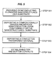
- the present invention is directed to methods for making the above-described compositionally-graded hybrid nanostructure-based photovoltaic devices, such methods comprising the steps of: (Step 501) providing a plurality of elongated semiconducting nanostructures on a substrate, the elongated semiconducting nanostructures having a doping of a first type; (Step 502) conformally-depositing an amorphous layer of semiconducting material on the elongated semicondcuting nanostructures such that they form an interface, wherein the amorphous layer is compositionally graded from substantially intrinsic at the interface to substantially conducting on the amorphous layer's opposing side, and wherein the graded composition of the amorphous layer is provided by a doping of a second type; (Step 503) depositing a conductive transparent material as a layer on the amorphous layer; and (Step 504) establishing top and bottom contacts operable for connecting the device to an external circuit.
- the elongated nanostructures are provided by growing them via a method selected from the group consisting of chemical vapor deposition (CVD), metal-organic chemical vapor deposition (MOCVD), plasma-enhanced chemical vapor deposition (PECVD), hot wire chemical vapor deposition (HWCVD), atomic layer deposition, electrochemical deposition, solution chemical deposition, and combinations thereof.
- CVD chemical vapor deposition
- MOCVD metal-organic chemical vapor deposition
- PECVD plasma-enhanced chemical vapor deposition
- HWCVD hot wire chemical vapor deposition
- atomic layer deposition electrochemical deposition
- electrochemical deposition solution chemical deposition, and combinations thereof.
- the elongated nanostructures are provided by catalytically growing them from metal nanoparticles, where the metal nanoparticles may reside in a nanoporous template, and wherein the metal nanoparticles may comprise a metal selected from the group consisting of gold (Au), indium (In), gallium (Ga), and iron (Fe).
- a nanoporous template is employed to grow elongated nanostructures such as is described in commonly-assigned United States Patent Application Serial No. 11/141,613, filed 27th May, 2005 .
- the step of conformally-depositing the amorphous layer is carried out using a technique selected from the group consisting of CVD, MOCVD, PECVD, HWCVD, sputtering, and combinations thereof.
- the amorphous layer is compositionally graded by doping with a dopant precursor that decomposes to a dopant species upon being deposited, and wherein the doping is provided in a graded manner during deposition by progressively increasing the dopant precursor concentration as the amorphous layer is deposited.
- Suitable dopant precursors include, but are not limited to, B 2 H 6 , B(CH 3 ) 3 , PH 3 , and the like.
- the present invention is directed to a solar panel comprising at least one compositionally-graded hybrid nanowire-based photovoltaic device, wherein the solar panel isolates such devices from their surrounding atmospheric environment and permits the generation of electrical power.
- a traditional (prior art) hybrid photovoltaic device is comprised of a semiconductor substrate of one conductivity type, and an amorphous semiconductor layer of the opposite conductivity type placed in contact with the substrate to form a heterojunction.
- the substrate may be n-type or p-type monocrystalline or polycrystalline semiconductor material.
- a compositionally-graded hybrid photovoltaic nanostructure-based device typically comprises a semiconductor nanowire (or nanostructure variant) film (or array) of one conductivity type on a semiconductor, metal, or glass substrate; and an amorphous semiconductor layer that is compositionally-graded across its thickness from substantially intrinsic at the interface with the substrate to substantially conductive at the opposite side.
- a heterojunction is formed when the amorphous semiconductor layer is compositionally-graded to the opposite conductivity type as that of the substrate.
- Compositional grading is achieved by adjusting the doping levels during fabrication of the amorphous semiconductor layer.
- the graded amorphous layering is generally disposed on the semiconductor nanowire/substrate surfaces in a conformal fashion.
- compositionally-graded layer distinguishes the approach described herein from that employed by Sanyo Electric Co. (see Background), the latter of which uses a combination of distinct, individual layers to form the hybrid device, none of which are on a nanowire film active layer (i.e., using nanowires as active PV elements).
- devices of the present invention comprise a single compositionally graded semiconductor layer with intrinsic properties at one surface region and conductive properties at the opposite surface region.
- the graded layer is formed between a thin film comprised of semiconductor nanowires grown on a substrate that acts as the absorber, and the transparent conducting coating that serves as the electrode.
- This single layer simultaneously provides three important features: (1) passivation of the nanowire surface, (2) elimination of extra interfaces inherent in multilayer structures, and (3) efficient separation of charge generated in the nanowires by virtue of the close proximity of the p-n junction. Combining these two characteristics using a single layer results in a unique design to minimize carrier recombination, and thereby maximize hybrid photovoltaic device performance.
- the compositionally graded single layer is fabricated such that the substantially intrinsic region is in contact with the nanowire thin film surfaces in a conformal fashion (see above). This provides the required surface passivation and thereby reduces charge carrier recombination.
- interface recombination is largely due to two effects.
- the first is structural: abrupt band bending at a heterojunction (e.g., a p/i or n/i junction) leads to a high density of interface states that result in charge carrier recombination.
- Grading the dopant concentration through a single layer provides continuous variation of localized states in the energy band gap. The gradual transition of localized energy states in the band gap eliminates abrupt band bending and reduces charge carrier recombination.
- the second is processing: during device fabrication interruptions between processing steps allow impurity atoms and/or spurious contaminants to be trapped in the interfaces of a multilayer structure. These defects can act as sites for charge carrier recombination that degrade device performance.
- the continuous formation of the single graded (in terms of dopant concentration) layer removes the discontinuity in the processing sequence, thereby eliminating the interface(s) of a multilayer design and reducing charge carrier recombination.
- This Example serves to illustrate process steps for fabricating compositionally graded hybrid nanowire photovoltaic devices, in accordance with some embodiments of the present invention.
- Silicon nanowire films of one conductivity type on glass, metal, or semiconductor substrate are placed in a plasma reaction chamber (e.g., a plasma enhanced chemical vapor deposition system).
- a vacuum pump removes atmospheric gases from the chamber.
- the substrates to be processed are preheated to 120 - 240°C.
- a hydrogen plasma surface preparation step is performed prior to the deposition of the compositionally graded layer.
- H 2 is introduced into the chamber at a flow rate of 50 - 500 sccm (standard cubic centimeters per minute).
- a throttle valve is used to maintain a constant processing pressure in the 200 - 800 mTorr range.
- Alternating frequency input power with a power density in the 6-50 mW/cm 2 range is used to ignite and maintain the plasma.
- Applied input power can be from 100 kHz to 2.45 GHz.
- Hydrogen plasma surface preparation time is 1 - 60 seconds.
- silane (SiH 4 ) is introduced into the process chamber at a flow rate of 10 - 60 sccm. This will initiate the deposition of the compositionally graded single amorphous semiconductor layer. Because no dopant precursors are included in the plasma, initially the composition of the amorphous layer is intrinsic (undoped), thus serving to passivate the surface of the semiconductor substrate. As the deposition process progresses, a dopant precursor is subsequently added to the plasma mixture. Examples of dopant precursors are: B 2 H 6 , B(CH 3 ) 3 , and PH 3 . These may be in pure form or diluted with a carrier gas such as argon, hydrogen or helium.
- a carrier gas such as argon, hydrogen or helium.
- the flow rate of the precursor is increased over the course of the compositionally graded layer deposition. This increasing dopant precursor flow forms a gradient in the doping concentration through the single amorphous layer (as it is deposited). At the conclusion of the graded layer deposition process, concentrations of dopant precursor in the plasma are such that substantially doped amorphous semiconductor properties are achieved.
- a p-type silicon nanowire film is used as the absorbing layer.
- the compositionally graded amorphous semiconductor single layer deposition is initiated.
- a mixture of pure hydrogen and silane may be used initially to form intrinsic (undoped) material properties that serve to passivate the substrate surface.
- a phosphorus-containing precursor is incrementally introduced to the plasma. Since phosphorus acts as a n-type dopant the amorphous material begins to take on n-type electrical properties. This process proceeds with increasing phosphorus-containing precursor flows until substantially conductive material properties are achieved. As a result, a compositionally graded layer comprising a phosphorus concentration that continuously varies across its thickness is obtained.
- the thickness of the graded layer is optimally ⁇ 200 ⁇ . In some such embodiments, this layer will form part of the front structure of the compositionally graded hybrid device. In other such embodiments, this layer will form part of the rear structure of the compositionally graded hybrid device (depending on the orientation of the device to a light source).
- a transparent conductive oxide (TCO) coating is deposited on the compositionally graded layers in order to form electrodes.
- These coatings may be, for example, indium tin oxide (ITO) or zinc oxide (ZnO).
- ITO indium tin oxide
- ZnO zinc oxide
- the TCO properties, including thickness, can be selected such that these layers act as antireflective (AR) coatings.
- Metal contacts e.g., Al, Ag, and the like are formed on the top and bottom (front and rear) electrodes so as to convey the electric current generated by the device.
- This Example serves to illustrate an exemplary application in which photovoltaic device 100 (or variants thereof) may find use, in accordance with some embodiments of the present invention.
- Photovoltaic modules containing a plurality of photovoltaic devices 100 are typically mounted onto the roofs of homes for grid-connected power generation.
- the modules are mounted by several methods to yield functional and aesthetic qualities.
- the module provides power that may be stored or sold back to the electric company for a profit, as is currently done with standard residential solar cell modules.
- the solar cells may be cut into standard sizes and mounted in a module frame and connected in series using standard solder-based interconnect schemes, in some cases with bypass diodes to minimize shading effects.
- the full glass substrate may be directly used in the framed module, or the glass may be laminated and used as the module without the need for a frame.
- a laser scribing method typically known in the art may be used for front and backside contact to interconnect solar cell segments in series.
- Si nanowires have been used in many of the embodiments described above, they are merely representative of a larger class of semiconductor-based elongated nanostructures. Accordingly, as will be recognized by one of skill in the art, many of the above-described embodiments can be varied to include elongated nanostructures comprising materials other than silicon. Such variant embodiments would have correspondingly different (from silicon) compositionally-graded amorphous layers.
- FIGURE 4 illustrates a variation on the conformal nature of the amorphous layer depicted in FIGURE 1.
- amorphous layer 403 substantially fills the voids between the nanotubes 101.
- a layer of transparent conductive material 404 can be deposited on the amorphous layer 403, as can top and bottom electrodes (not shown).
- the present invention is directed to compositionally-graded hybrid nanostructure-based photovoltaic devices comprising elongated semiconductor nanostructures and an amorphous semiconductor single layer with continuous gradation of doping concentration across its thickness from substantially intrinsic to substantially conductive.
- the present invention is directed to methods of making such photovoltaic devices, as well as to applications which utilize such devices (e.g., solar cell modules).
- the present invention provides for the use of a continuous, compositionally graded single semiconductor layer whose intrinsic properties near one surface region provide passivation of the semiconductor substrate reduce charge carrier recombination, and whose conductive properties near the opposite surface region provide the electrical characteristics required to form an electronic or opto-electronic device.
- the present invention provides for the removal of the interface between an intrinsic amorphous layer and a conductive amorphous layer where charge carrier recombination may occur.
- the present invention provides for removal of impurity atoms and/or spurious contaminants at the interface between an intrinsic amorphous layer and a conductive amorphous layer formed during device fabrication that result in increased charge carrier recombination.
- the present invention provides gradation of localized energy states in the energy band gap of the compositionally graded single amorphous layer, wherein this eliminates discontinuities in localized energy states that cause charge carrier recombination at the interface(s) between layers with different band gaps and/or conductivity types.
- the present invention provides for utilization of a one-step plasma deposition process for fabricating a compositionally-graded single layer.
Landscapes
- Photovoltaic Devices (AREA)
Applications Claiming Priority (1)
| Application Number | Priority Date | Filing Date | Title |
|---|---|---|---|
| US11/599,722 US20080135089A1 (en) | 2006-11-15 | 2006-11-15 | Graded hybrid amorphous silicon nanowire solar cells |
Publications (1)
| Publication Number | Publication Date |
|---|---|
| EP1923918A2 true EP1923918A2 (en) | 2008-05-21 |
Family
ID=39103185
Family Applications (1)
| Application Number | Title | Priority Date | Filing Date |
|---|---|---|---|
| EP07120384A Withdrawn EP1923918A2 (en) | 2006-11-15 | 2007-11-09 | Graded hybrid amorphous silicon nanowire solar cells |
Country Status (5)
| Country | Link |
|---|---|
| US (1) | US20080135089A1 (enExample) |
| EP (1) | EP1923918A2 (enExample) |
| JP (1) | JP2008177539A (enExample) |
| KR (1) | KR20080044181A (enExample) |
| CN (1) | CN101183689B (enExample) |
Cited By (4)
| Publication number | Priority date | Publication date | Assignee | Title |
|---|---|---|---|---|
| WO2008156421A3 (en) * | 2007-06-19 | 2009-02-26 | Qunano Ab | Nanowire-based solar cell structure |
| GB2462108A (en) * | 2008-07-24 | 2010-01-27 | Sharp Kk | Deposition of a thin film on a nanostructured surface |
| WO2011092601A3 (en) * | 2010-01-29 | 2011-11-10 | King Abdullah University Of Science And Technology | Bio-inspired nanostructures for implementing vertical pn-junctions |
| EP2615649A3 (en) * | 2012-01-10 | 2013-10-23 | The Boeing Company | Lateral solar cell structure |
Families Citing this family (79)
| Publication number | Priority date | Publication date | Assignee | Title |
|---|---|---|---|---|
| KR100593264B1 (ko) * | 2003-06-26 | 2006-06-26 | 학교법인 포항공과대학교 | p-타입 반도체 박막과 n-타입 산화아연(ZnO)계나노막대의 이종접합 구조체, 이의 제법 및 이를 이용한소자 |
| US8003883B2 (en) * | 2007-01-11 | 2011-08-23 | General Electric Company | Nanowall solar cells and optoelectronic devices |
| US20080264479A1 (en) * | 2007-04-25 | 2008-10-30 | Nanoco Technologies Limited | Hybrid Photovoltaic Cells and Related Methods |
| KR101503557B1 (ko) * | 2007-09-25 | 2015-03-17 | 퍼스트 솔라, 인코포레이티드 | 계면 층을 포함한 광기전 장치 |
| US8106289B2 (en) * | 2007-12-31 | 2012-01-31 | Banpil Photonics, Inc. | Hybrid photovoltaic device |
| KR100935322B1 (ko) * | 2008-01-02 | 2010-01-06 | 삼성전기주식회사 | 고효율 태양전지 및 이의 제조방법 |
| CN101561194B (zh) * | 2008-04-18 | 2010-12-29 | 清华大学 | 太阳能集热器 |
| US7902540B2 (en) * | 2008-05-21 | 2011-03-08 | International Business Machines Corporation | Fast P-I-N photodetector with high responsitivity |
| WO2009151979A2 (en) * | 2008-06-09 | 2009-12-17 | 4Power, Llc | High-efficiency solar cell structures and methods |
| US20100012190A1 (en) * | 2008-07-16 | 2010-01-21 | Hajime Goto | Nanowire photovoltaic cells and manufacture method thereof |
| KR101613083B1 (ko) * | 2008-08-21 | 2016-04-20 | 삼성전자주식회사 | 디지털 저작권 관리에서 컨텐츠 정보를 사용하기 위한 장치및 방법 |
| US20100139747A1 (en) * | 2008-08-28 | 2010-06-10 | The Penn State Research Foundation | Single-crystal nanowires and liquid junction solar cells |
| KR101002682B1 (ko) * | 2008-08-28 | 2010-12-21 | 삼성전기주식회사 | 태양전지 및 그 제조방법 |
| WO2010071658A1 (en) * | 2008-12-19 | 2010-06-24 | Hewlett-Packard Development Company, Hewlett-Packard Development Company, L.P. | Photovoltaic structure and method of fabrication employing nanowire on stub |
| CN102325719A (zh) * | 2008-12-30 | 2012-01-18 | 3M创新有限公司 | 纳米结构化制品和制备纳米结构化制品的方法 |
| KR101915868B1 (ko) * | 2008-12-30 | 2018-11-06 | 쓰리엠 이노베이티브 프로퍼티즈 컴파니 | 반사방지 용품 및 이의 제조 방법 |
| TWI447917B (zh) * | 2009-01-10 | 2014-08-01 | Nexpower Technology Corp | 薄膜太陽能電池及其前電極層之製作方法 |
| KR101040956B1 (ko) * | 2009-02-26 | 2011-06-16 | 전자부품연구원 | 산화아연 나노와이어를 이용한 박막 실리콘 태양전지 및 그의 제조방법 |
| US20110124146A1 (en) * | 2009-05-29 | 2011-05-26 | Pitera Arthur J | Methods of forming high-efficiency multi-junction solar cell structures |
| US8211735B2 (en) * | 2009-06-08 | 2012-07-03 | International Business Machines Corporation | Nano/microwire solar cell fabricated by nano/microsphere lithography |
| KR101033028B1 (ko) * | 2009-06-25 | 2011-05-09 | 한양대학교 산학협력단 | 태양 전지 및 그 제조 방법 |
| US8933526B2 (en) * | 2009-07-15 | 2015-01-13 | First Solar, Inc. | Nanostructured functional coatings and devices |
| KR101103264B1 (ko) * | 2009-07-29 | 2012-01-11 | 한국기계연구원 | 기능성 표면의 제조방법 |
| WO2011019608A1 (en) * | 2009-08-10 | 2011-02-17 | First Solar, Inc | Photovoltaic device back contact |
| KR20110018764A (ko) | 2009-08-18 | 2011-02-24 | 삼성전자주식회사 | 나노와이어를 포함하는 태양전지 및 나노와이어의 형성방법 |
| DE102009029017A1 (de) * | 2009-08-31 | 2011-03-03 | Robert Bosch Gmbh | Halbleiter-Schichtmaterial und Heteroübergangs-Solarzelle |
| KR101539670B1 (ko) | 2009-10-13 | 2015-07-27 | 삼성전자주식회사 | 전기에너지 발생장치 |
| WO2011066570A2 (en) * | 2009-11-30 | 2011-06-03 | California Institute Of Technology | Semiconductor wire array structures, and solar cells and photodetectors based on such structures |
| KR101658534B1 (ko) * | 2009-12-15 | 2016-09-23 | 엘지디스플레이 주식회사 | 태양전지 및 그 제조방법 |
| KR101652406B1 (ko) * | 2010-02-19 | 2016-08-30 | 삼성전자주식회사 | 전기 에너지 발생 장치 |
| WO2011156042A2 (en) | 2010-03-23 | 2011-12-15 | California Institute Of Technology | Heterojunction wire array solar cells |
| KR101069066B1 (ko) | 2010-04-23 | 2011-09-29 | 전북대학교산학협력단 | 알루미늄이 도핑된 산화아연 나노로드 기반 실리콘 태양전지의 투명전도성기판 제조방법 |
| US8431817B2 (en) * | 2010-06-08 | 2013-04-30 | Sundiode Inc. | Multi-junction solar cell having sidewall bi-layer electrical interconnect |
| US8476637B2 (en) | 2010-06-08 | 2013-07-02 | Sundiode Inc. | Nanostructure optoelectronic device having sidewall electrical contact |
| US8659037B2 (en) | 2010-06-08 | 2014-02-25 | Sundiode Inc. | Nanostructure optoelectronic device with independently controllable junctions |
| KR20130136906A (ko) | 2010-06-18 | 2013-12-13 | 글로 에이비 | 나노와이어 led 구조와 이를 제조하기 위한 방법 |
| US9249017B2 (en) * | 2010-07-12 | 2016-02-02 | Board Of Regents, The University Of Texas System | Nanowires and methods of making and using |
| TWI400352B (zh) * | 2010-07-29 | 2013-07-01 | Atomic Energy Council | 提純冶金級矽基板矽奈米線太陽電池元件之製備方法 |
| TWI424575B (zh) * | 2010-08-02 | 2014-01-21 | Univ Feng Chia | A solar cell having an electrode of a micrometer or micrometer or lower conductive line |
| WO2012067687A2 (en) * | 2010-08-26 | 2012-05-24 | The Ohio State University | Nanoscale emitters with polarization grading |
| WO2012035243A1 (fr) * | 2010-09-14 | 2012-03-22 | Commissariat A L'energie Atomique Et Aux Energies Alternatives | Dispositif optoelectronique a base de nanofils pour l'émission de lumière |
| US8207013B2 (en) * | 2010-09-17 | 2012-06-26 | Atomic Energy Council Institute Of Nuclear Energy Research | Method of fabricating silicon nanowire solar cell device having upgraded metallurgical grade silicon substrate |
| US8604330B1 (en) | 2010-12-06 | 2013-12-10 | 4Power, Llc | High-efficiency solar-cell arrays with integrated devices and methods for forming them |
| WO2012078063A1 (en) * | 2010-12-09 | 2012-06-14 | Faculdade De Ciências E Tecnologia Da Universidade Nova De Lisboa | Mesoscopic optoelectronic devices comprising arrays of semiconductor pillars deposited from a suspension and production method thereof |
| US20140096816A1 (en) * | 2010-12-22 | 2014-04-10 | Harry A. Atwater | Heterojunction microwire array semiconductor devices |
| FR2972852B1 (fr) * | 2011-03-17 | 2013-04-12 | Commissariat Energie Atomique | Dispositif a base de nano/microfils stabilise mecaniquement et aux proprietes optiques ameliorees et son procede de realisation |
| WO2013130027A1 (en) * | 2011-05-20 | 2013-09-06 | Zena Technologies, Inc. | Light absorption and filtering properties of vertically oriented semiconductor nano wires |
| EP2717322A4 (en) * | 2011-05-25 | 2015-01-21 | Hitachi Ltd | SOLAR CELL |
| US20120298169A1 (en) * | 2011-05-26 | 2012-11-29 | Guo George X | Multi-junction Photovoltaic Cells |
| WO2013003828A2 (en) * | 2011-06-30 | 2013-01-03 | California Institute Of Technology | A tandem solar cell using a silicon microwire array and amorphous silicon photovoltaic layer |
| DK2736837T3 (da) * | 2011-07-26 | 2021-10-25 | Oned Mat Inc | Fremgangsmåde til fremstilling af nanosiliciumtråde |
| KR101120009B1 (ko) * | 2011-08-03 | 2012-03-16 | 한국기계연구원 | 나노 돌기를 갖는 태양 전지 및 이의 제조 방법 |
| KR101316375B1 (ko) | 2011-08-19 | 2013-10-08 | 포항공과대학교 산학협력단 | 태양전지 및 이의 제조방법 |
| CN102368506A (zh) * | 2011-09-26 | 2012-03-07 | 浙江大学 | 一种n-氧化锌/p-硅纳米线三维异质结太阳能转换装置 |
| US8350249B1 (en) * | 2011-09-26 | 2013-01-08 | Glo Ab | Coalesced nanowire structures with interstitial voids and method for manufacturing the same |
| US9035278B2 (en) | 2011-09-26 | 2015-05-19 | Glo Ab | Coalesced nanowire structures with interstitial voids and method for manufacturing the same |
| US20130081679A1 (en) * | 2011-09-30 | 2013-04-04 | Ut-Battelle, Llc | Multijunction hybrid solar cell incorporating vertically-aligned silicon nanowires with thin films |
| KR101435458B1 (ko) * | 2011-12-12 | 2014-09-01 | 동국대학교 산학협력단 | 나노로드를 이용한 태양전지 및 그의 제조 방법 |
| CN102569508B (zh) * | 2011-12-29 | 2014-10-22 | 中山大学 | 一种纳米线阵列结构薄膜太阳能光伏电池及其制备方法 |
| WO2013126432A1 (en) | 2012-02-21 | 2013-08-29 | California Institute Of Technology | Axially-integrated epitaxially-grown tandem wire arrays |
| WO2013152043A1 (en) | 2012-04-02 | 2013-10-10 | California Institute Of Technology | Solar fuels generator |
| WO2013152132A1 (en) * | 2012-04-03 | 2013-10-10 | The California Institute Of Technology | Semiconductor structures for fuel generation |
| CN102637755B (zh) * | 2012-04-28 | 2014-05-07 | 中山大学 | 一种纳米结构czts薄膜光伏电池及其制备方法 |
| WO2013190646A1 (ja) * | 2012-06-20 | 2013-12-27 | 株式会社日立製作所 | 太陽電池セルおよびその製造方法 |
| CN102856430B (zh) * | 2012-07-25 | 2015-04-22 | 常州大学 | 一种铁酸铋纳米线太阳能电池的制备方法 |
| CN102891191A (zh) * | 2012-09-29 | 2013-01-23 | 中国科学院半导体研究所 | 非晶硅中间带太阳能电池及其制备方法 |
| US9553223B2 (en) | 2013-01-24 | 2017-01-24 | California Institute Of Technology | Method for alignment of microwires |
| KR101590224B1 (ko) * | 2013-04-11 | 2016-01-29 | 제일모직주식회사 | 태양전지 전극 형성용 조성물 및 이로부터 제조된 전극 |
| GB2517186A (en) * | 2013-08-14 | 2015-02-18 | Norwegian University Of Science And Technology | Radial P-N junction nanowire solar cells |
| JPWO2017145906A1 (ja) * | 2016-02-25 | 2018-12-27 | 株式会社ソシオネクスト | 半導体集積回路装置 |
| FR3048241B1 (fr) * | 2016-02-29 | 2021-12-31 | Commissariat Energie Atomique | Procede de preparation de nanofils de silicium et/ou de germanium |
| ES3032418T3 (en) | 2016-07-15 | 2025-07-18 | Oned Mat Inc | Manufacturing apparatus and method for making silicon nanowires on carbon based powders for use in batteries |
| CN107331715B (zh) * | 2017-07-03 | 2020-06-30 | 京东方科技集团股份有限公司 | 一种太阳能电池及其制作方法 |
| US10490682B2 (en) | 2018-03-14 | 2019-11-26 | National Mechanical Group Corp. | Frame-less encapsulated photo-voltaic solar panel supporting solar cell modules encapsulated within multiple layers of optically-transparent epoxy-resin materials |
| US11362229B2 (en) * | 2018-04-04 | 2022-06-14 | California Institute Of Technology | Epitaxy-free nanowire cell process for the manufacture of photovoltaics |
| US11041338B2 (en) | 2018-08-21 | 2021-06-22 | California Institute Of Technology | Windows implementing effectively transparent conductors and related methods of manufacturing |
| CN111863933B (zh) * | 2019-04-29 | 2023-07-14 | 中芯国际集成电路制造(上海)有限公司 | 半导体结构及其形成方法 |
| US12402418B2 (en) | 2020-06-12 | 2025-08-26 | California Institute Of Technology | Systems and methods for non-epitaxial high Schottky-barrier heterojunction solar cells |
| CN115271223A (zh) * | 2022-08-04 | 2022-11-01 | 国网安徽省电力有限公司宣城供电公司 | 基于工业园区屋顶最大利用面积的太阳能资源评估方法 |
Family Cites Families (14)
| Publication number | Priority date | Publication date | Assignee | Title |
|---|---|---|---|---|
| EP0198196B1 (de) * | 1985-04-11 | 1993-02-03 | Siemens Aktiengesellschaft | Solarzelle mit einem aus amorphen Silizium bestehenden Halbleiterkörper der Schichtenfolge p-SiC/i/n |
| US5213628A (en) * | 1990-09-20 | 1993-05-25 | Sanyo Electric Co., Ltd. | Photovoltaic device |
| JP2719230B2 (ja) * | 1990-11-22 | 1998-02-25 | キヤノン株式会社 | 光起電力素子 |
| JPH0878659A (ja) * | 1994-09-02 | 1996-03-22 | Sanyo Electric Co Ltd | 半導体デバイス及びその製造方法 |
| JP3876021B2 (ja) * | 1995-08-22 | 2007-01-31 | 松下電器産業株式会社 | シリコン構造体、その製造方法及びその製造装置、並びにシリコン構造体を用いた太陽電池 |
| JP3490964B2 (ja) * | 2000-09-05 | 2004-01-26 | 三洋電機株式会社 | 光起電力装置 |
| JP3702240B2 (ja) * | 2002-03-26 | 2005-10-05 | 三洋電機株式会社 | 半導体素子及びその製造方法 |
| US6878871B2 (en) * | 2002-09-05 | 2005-04-12 | Nanosys, Inc. | Nanostructure and nanocomposite based compositions and photovoltaic devices |
| US7015640B2 (en) * | 2002-09-11 | 2006-03-21 | General Electric Company | Diffusion barrier coatings having graded compositions and devices incorporating the same |
| US6969897B2 (en) * | 2002-12-10 | 2005-11-29 | Kim Ii John | Optoelectronic devices employing fibers for light collection and emission |
| US20050072456A1 (en) * | 2003-01-23 | 2005-04-07 | Stevenson Edward J. | Integrated photovoltaic roofing system |
| US20060207647A1 (en) * | 2005-03-16 | 2006-09-21 | General Electric Company | High efficiency inorganic nanorod-enhanced photovoltaic devices |
| WO2006138671A2 (en) * | 2005-06-17 | 2006-12-28 | Illuminex Corporation | Photovoltaic wire |
| US7635600B2 (en) * | 2005-11-16 | 2009-12-22 | Sharp Laboratories Of America, Inc. | Photovoltaic structure with a conductive nanowire array electrode |
-
2006
- 2006-11-15 US US11/599,722 patent/US20080135089A1/en not_active Abandoned
-
2007
- 2007-11-09 EP EP07120384A patent/EP1923918A2/en not_active Withdrawn
- 2007-11-14 KR KR1020070115979A patent/KR20080044181A/ko not_active Withdrawn
- 2007-11-15 CN CN2007101944570A patent/CN101183689B/zh not_active Expired - Fee Related
- 2007-11-15 JP JP2007296263A patent/JP2008177539A/ja active Pending
Cited By (9)
| Publication number | Priority date | Publication date | Assignee | Title |
|---|---|---|---|---|
| WO2008156421A3 (en) * | 2007-06-19 | 2009-02-26 | Qunano Ab | Nanowire-based solar cell structure |
| US10128394B2 (en) | 2007-06-19 | 2018-11-13 | Qunano Ab | Nanowire-based solar cell structure |
| GB2462108A (en) * | 2008-07-24 | 2010-01-27 | Sharp Kk | Deposition of a thin film on a nanostructured surface |
| EP2319069A4 (en) * | 2008-07-24 | 2013-01-09 | Sharp Kk | METHOD FOR BREEDING A THIN FILM, METHOD FOR PRODUCING A STRUCTURE AND DEVICE |
| US8778781B2 (en) | 2008-07-24 | 2014-07-15 | Sharp Kabushiki Kaisha | Method of growing a thin film, a method of forming a structure and a device |
| WO2011092601A3 (en) * | 2010-01-29 | 2011-11-10 | King Abdullah University Of Science And Technology | Bio-inspired nanostructures for implementing vertical pn-junctions |
| EP2615649A3 (en) * | 2012-01-10 | 2013-10-23 | The Boeing Company | Lateral solar cell structure |
| US9911886B2 (en) | 2012-01-10 | 2018-03-06 | The Boeing Company | Lateral solar cell structure |
| TWI667799B (zh) * | 2012-01-10 | 2019-08-01 | 美商波音公司 | 橫向太陽能電池結構 |
Also Published As
| Publication number | Publication date |
|---|---|
| CN101183689A (zh) | 2008-05-21 |
| KR20080044181A (ko) | 2008-05-20 |
| CN101183689B (zh) | 2012-08-01 |
| US20080135089A1 (en) | 2008-06-12 |
| JP2008177539A (ja) | 2008-07-31 |
Similar Documents
| Publication | Publication Date | Title |
|---|---|---|
| EP1923918A2 (en) | Graded hybrid amorphous silicon nanowire solar cells | |
| AU2007254673B2 (en) | Nanowall solar cells and optoelectronic devices | |
| AU2007234548B2 (en) | Amorphous-crystalline tandem nanostructured solar cells | |
| US7977568B2 (en) | Multilayered film-nanowire composite, bifacial, and tandem solar cells | |
| AU2007211902B2 (en) | Nanowires in thin-film silicon solar cells | |
| EP1892769A2 (en) | Single conformal junction nanowire photovoltaic devices | |
| US8912424B2 (en) | Multi-junction photovoltaic device and fabrication method | |
| US20100229927A1 (en) | Heterojunction solar cell based on epitaxial crystalline-silicon thin film on metallurgical silicon substrate design | |
| CN1402361A (zh) | 光电装置 | |
| CN102456763A (zh) | 包含异质结的光电子器件 | |
| Wanlass et al. | High-performance, 0.6-eV, Ga 0.32 In 0.68 As/InAs 0.32 P 0.68 thermophotovoltaic converters and monolithically interconnected modules |
Legal Events
| Date | Code | Title | Description |
|---|---|---|---|
| PUAI | Public reference made under article 153(3) epc to a published international application that has entered the european phase |
Free format text: ORIGINAL CODE: 0009012 |
|
| AK | Designated contracting states |
Kind code of ref document: A2 Designated state(s): AT BE BG CH CY CZ DE DK EE ES FI FR GB GR HU IE IS IT LI LT LU LV MC MT NL PL PT RO SE SI SK TR |
|
| AX | Request for extension of the european patent |
Extension state: AL BA HR MK RS |
|
| STAA | Information on the status of an ep patent application or granted ep patent |
Free format text: STATUS: THE APPLICATION IS DEEMED TO BE WITHDRAWN |
|
| 18D | Application deemed to be withdrawn |
Effective date: 20130601 |