EP1918069A1 - Double side polishing method for wafer - Google Patents
Double side polishing method for wafer Download PDFInfo
- Publication number
- EP1918069A1 EP1918069A1 EP06767473A EP06767473A EP1918069A1 EP 1918069 A1 EP1918069 A1 EP 1918069A1 EP 06767473 A EP06767473 A EP 06767473A EP 06767473 A EP06767473 A EP 06767473A EP 1918069 A1 EP1918069 A1 EP 1918069A1
- Authority
- EP
- European Patent Office
- Prior art keywords
- slurry
- wafer
- polishing
- supply holes
- amount
- Prior art date
- Legal status (The legal status is an assumption and is not a legal conclusion. Google has not performed a legal analysis and makes no representation as to the accuracy of the status listed.)
- Granted
Links
Images




Classifications
-
- B—PERFORMING OPERATIONS; TRANSPORTING
- B24—GRINDING; POLISHING
- B24B—MACHINES, DEVICES, OR PROCESSES FOR GRINDING OR POLISHING; DRESSING OR CONDITIONING OF ABRADING SURFACES; FEEDING OF GRINDING, POLISHING, OR LAPPING AGENTS
- B24B37/00—Lapping machines or devices; Accessories
- B24B37/04—Lapping machines or devices; Accessories designed for working plane surfaces
- B24B37/07—Lapping machines or devices; Accessories designed for working plane surfaces characterised by the movement of the work or lapping tool
- B24B37/08—Lapping machines or devices; Accessories designed for working plane surfaces characterised by the movement of the work or lapping tool for double side lapping
-
- B—PERFORMING OPERATIONS; TRANSPORTING
- B24—GRINDING; POLISHING
- B24B—MACHINES, DEVICES, OR PROCESSES FOR GRINDING OR POLISHING; DRESSING OR CONDITIONING OF ABRADING SURFACES; FEEDING OF GRINDING, POLISHING, OR LAPPING AGENTS
- B24B37/00—Lapping machines or devices; Accessories
- B24B37/04—Lapping machines or devices; Accessories designed for working plane surfaces
-
- B—PERFORMING OPERATIONS; TRANSPORTING
- B24—GRINDING; POLISHING
- B24B—MACHINES, DEVICES, OR PROCESSES FOR GRINDING OR POLISHING; DRESSING OR CONDITIONING OF ABRADING SURFACES; FEEDING OF GRINDING, POLISHING, OR LAPPING AGENTS
- B24B57/00—Devices for feeding, applying, grading or recovering grinding, polishing or lapping agents
-
- H—ELECTRICITY
- H10—SEMICONDUCTOR DEVICES; ELECTRIC SOLID-STATE DEVICES NOT OTHERWISE PROVIDED FOR
- H10P—GENERIC PROCESSES OR APPARATUS FOR THE MANUFACTURE OR TREATMENT OF DEVICES COVERED BY CLASS H10
- H10P52/00—Grinding, lapping or polishing of wafers, substrates or parts of devices
-
- H—ELECTRICITY
- H10—SEMICONDUCTOR DEVICES; ELECTRIC SOLID-STATE DEVICES NOT OTHERWISE PROVIDED FOR
- H10P—GENERIC PROCESSES OR APPARATUS FOR THE MANUFACTURE OR TREATMENT OF DEVICES COVERED BY CLASS H10
- H10P90/00—Preparation of wafers not covered by a single main group of this subclass, e.g. wafer reinforcement
- H10P90/12—Preparing bulk and homogeneous wafers
- H10P90/129—Preparing bulk and homogeneous wafers by polishing
Definitions
- the present invention relates to a method of polishing both surfaces of a wafer, and more particularly to a double-side polishing method which can suppress outer peripheral sag of a wafer by improving a method of supplying a slurry to the wafer.
- FIG. 8 is a schematic explanatory drawing showing an example of a conventional double-side polishing apparatus.
- a double-side polishing apparatus 201 is an apparatus which enables rotation and revolution of a carrier 208 meshed between a sun gear 206 and an internal gear 207 by driving rotation of the sun gear 206 and rotates a lower turn table 202 and an upper turn table 203 in opposite directions to simultaneously polish both surfaces of a wafer W by polishing pads 204 attached to the upper and lower turn tables.
- a slurry supplying mechanism that supplies to a wafer W a slurry which increases a polishing efficiency for the wafer W and reduces heat generated in the upper and lower turn tables 202 and 203 is provided in the double-side polishing apparatus 201.
- This slurry supplying mechanism is a mechanism that supplies a slurry to slurry supply holes 205 provided in the upper turn table 203 from a slurry tank 209 through a slurry supply duct 210, powder rings 212, and slurry supply tubes 213 and allows the slurry to flow out from lower end openings of the slurry supply holes 205 toward the wafer W.
- both surfaces of a wafer are polished while uniformly supplying the same amount of slurry from each supply hole by using such a double-side polishing apparatus.
- Japanese Patent Application Laid-open No. 2004-142040 or Japanese Patent Application Laid-open No. H11-262862 discloses a double-side polishing method using a double-side polishing apparatus having a different structure adopting, e.g., a compression transport scheme in relation to a slurry supply scheme.
- the amount of the slurry supplied from the supply holes provided on the outer side of the upper turn table is twice or more of the amount of the slurry supplied from the slurry supply holes provided on the inner side of the same.
- the amount of the slurry supplied from the supply holes provided on the outer side of the upper turn table is twice or more of the amount of the slurry supplied from the slurry supply holes provided on the inner side of the same in this manner, the outer peripheral sag of the wafer can be more assuredly suppressed, thereby providing the high-quality wafer with a high degree of flatness. Further, since the slurry can be supplied from the supply holes on the inner side and the outer side of the upper turn table at a more appropriate rate, productivity of the wafer can be further improved.
- both surfaces of a processing target wafer can be polished to provide a high-quality wafer in which sag at an outer periphery is suppressed. Furthermore, since the slurry can be appropriately adjusted in terms of supply positions and amounts and supplied to a space between the upper and lower turn tables at the time of polishing, sag at the wafer outer peripheral portion can be arbitrarily controlled, thus improving productivity of the wafer.
- the present inventors has revealed that, by supplying a slurry in such a manner that an amount of the slurry supplied from slurry supply holes provided on an outer side relative to the center of rotation of an upper turn table becomes larger than an amount of the slurry supplied from slurry supply holes provided on an inner side relative to the same, a polishing amount at an outer peripheral portion of the wafer can be adjusted to obtain the high-quality wafer in which sag at the outer peripheral portion thereof is suppressed and the slurry can be appropriately supplied to polish both surfaces of a wafer efficiently, and hence they have brought the present invention to completion.
- FIG. 1 is a schematic explanatory drawing showing an example of a double-side polishing apparatus, which can be used when carrying out a double-side polishing method according to the present invention.
- This double-side polishing apparatus 1 includes a lower turn table 2 and an upper turn table 3 which are vertically provided to face each other, and polishing pads 4 are attached to opposed sides of the respective turn tables 2 and 3.
- a plurality of slurry supply holes 5 and 5' from which a polishing slurry is supplied are provided in the upper turn table 3 on an inner side and an outer side relative to the center of rotation of the upper turn table 3.
- a sun gear 6 is provided at a central part between the upper turn table 3 and the lower turn table 2
- an internal gear 7 is provided at a rim portion
- a processing target wafer W is held in a holding hole of a carrier 8 and sandwiched between the upper turn table 3 and the lower turn table 2.
- a planetary type double-side polishing apparatus is used in this example, but the present invention is not restricted to the planetary type, and an swinging type double-side polishing apparatus may be adopted, for example.
- a supplying mechanism for a slurry will now be explained.
- the slurry supplied to a space between the upper and lower turn tables at the time of double-side polishing is stored in a slurry tank 9, and a slurry supply duct 10 through which the slurry is supplied is extended from this slurry tank 9. Further, this supply duct 10 diverges into two toward the supply holes 5 provided on the inner side relative to the center of rotation of the upper turn table 3 and the supply holes 5' provided on the outer side relative to the same. Valves 11 and 11' which are used to adjust flow volumes of the slurry are arranged in the diverging supply ducts, respectively.
- Each diverging supply duct 10 is coupled with three slurry supply tubes 13 with a powder ring 12 interposed, and the other end of each supply tube 13 is connected with each supply hole 5 or 5' in the upper turn table 3.
- an amount of the slurry supplied from the supply holes 5' placed on the outer side can be adjusted to be larger than an amount of the slurry supplied from the supply holes 5 placed on the inner side.
- valves 11 and 11' or the powder rings 12 a mechanism which can appropriately control a flow volume of the slurry or that which can divide and flow the slurry to each supply tube 13 without clogging can suffice, and these members are not restricted in particular.
- the supply duct 10 diverges first into two from the slurry tank 9 in this example, but it may diverge in accordance with the number of the supply holes 5 and 5' provided in the upper turn table 3, valves may be provided in the respective diverging supply ducts 10, and these ducts may be coupled with the supply tubes 13 to be connected with the supply holes so that supply amounts of the slurry can be individually adjusted in accordance with the respective supply holes, for example.
- the double-side polishing apparatus which can be used in the present invention is not restricted to the above apparatus, and any apparatus can be adopted as long as it has a structure where the slurry can be supplied in such a manner that an amount of the slurry supplied from the slurry supply holes 5' provided on the outer side relative to the center of rotation of the upper turn table becomes larger than an amount of the slurry supplied from the slurry supply holes 5 provided on the inner side relative to the same.
- a method of polishing both surfaces of a wafer W based on the double-side polishing method according to the present invention will now be explained in relation to an example where the double-side polishing apparatus 1 depicted in FIG. 1 is used.
- the processing target wafer W is held in the carrier 8, and the carrier 8 is sandwiched between the upper turn table 3 and the lower turn table 2.
- Outer peripheral teeth of the carrier 8 mesh with respective tooth portions of the sun gear 6 and the internal gear 7, and the carrier 8 rotates around the sun gear 6 while rotating on its axis when the upper turn table 3 and the lower turn table 2 are rotated by a non-illustrated driving source.
- both surfaces of the wafer W held in the carrier 8 are simultaneously polished by the polishing pads 4 attached to the upper and lower turn tables 2 and 3.
- the slurry is supplied from the supply holes 5 and 5'. It is to be noted that the present invention is not restricted to such a planetary type as explained above.
- the slurry stored in the slurry tank 9 is flowed through the supply duct 10 and divided into two directions.
- One is a flow path leading to the supply holes 5 provided on the inner side relative to the center of rotation of the upper turn table 3, and the other is a flow path leading to the supply holes 5' provided on the outer side.
- the valves 11 and 11' provided in the respective diverging supply ducts 10 are used to independently control flow volumes of the slurry flowing through the respective flow paths.
- the flow paths are further divided by the powder rings 12, and the slurry is supplied to the wafer W between the upper and lower turn tables 2 and 3 from the respective supply holes 5 and 5' via the respective supply tubes 13.
- the flow volumes of the slurry flowing through the respective supply ducts 10 leading to the supply holes 5 and 5' on the inner and outer sides are adjusted by using the valves 11 and 11' in such a manner that an amount supplied to the space between the upper and lower turn tables 2 and 3 from the supply holes 5' provided on the outer side becomes larger than an amount supplied from the supply holes 5 provided on the inner side.
- the same amounts of the slurry are supplied from the respective supply holes in the conventional example, it is good enough to supply a larger amount of the slurry from at least one of the supply holes 5' on the outer side than amounts supplied from the other supply holes so that the supply amount of the slurry from the supply holes 5' on the outer side becomes larger than the amount of the slurry supplied from the supply holes 5 on the inner side.
- the supply holes 5 and 5' on the inner and outer sides can be divided at, e.g., a position corresponding to 1/2 of a radius of the upper turn table 3.
- a polishing amount at the outer peripheral portion of the processing target wafer can be adjusted, and the high-quality wafer in which outer peripheral sag of the wafer is suppressed can be obtained, thereby improving a production yield. Furthermore, when a rate of the amounts of the slurry supplied to the inner side and the outer side is changed, an amount of sag at the outer peripheral portion can be controlled so that double-side polishing can be performed to obtain the wafer having a desired shape. Therefore, the high-quality wafer without outer peripheral sag can be obtained, and productivity of the wafer can be improved.
- Supply amounts of a slurry from supply holes provided on an inner side and an outer side relative to the center of rotation of an upper turn table were individually set/adjusted and both surfaces of each sample wafer were polished by using the double-side polishing apparatus depicted in FIG. 1 .
- an amount fed from a slurry tank was set to 3.5 1/min, and five patterns of a rate of a total amount supplied from supply holes 5 provided on the inner side of the upper turn table and a total amount supplied from supply holes 5' provided on the outer side of the same, i.e., 3:1 (Comparative Example 1), 2:1 (Comparative Example 2), 1:1 (Comparative Example 3), 1:2 (Example 1), and 1:3 (Example 2) were prepared.
- each sample wafer a P-type highly-doped product having a diameter of 300 mm, an orientation ⁇ 100>, and a resistivity of 0.01 ⁇ cm was prepared as each sample wafer.
- a polyurethane foam was used for a polishing pad, and colloidal silica was used as the slurry.
- each sample wafer was held in a carrier and sandwiched between upper and lower turn tables, the upper and lower turn tables were rotated in opposite directions at a rotating speed of 35 rpm with a polishing pressure of 140 g/cm 2 while supplying the slurry, both surfaces of the sample wafer were polished in each of the five slurry supply scheme patterns, and a shape of the polished sample wafer was measured to obtain outer peripheral sag.
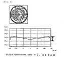
- FIG. 2 (Comparative Example 1), FIG. 3 (Comparative Example 2), FIG. 4 (Comparative Example 3), FIG. 5 (Example 1), FIG. 6 (Example 2), and FIG. 7 show measurement results of Examples 1 and 2 and Comparative Examples 1 to 3.
- FIGS. 2 to 6 show shapes of polished sample wafers (contour maps and cross-sectional shapes). Additionally, FIG. 7 shows an outer peripheral sag amount in each example in the form of a graph, and a relationship between a slurry supply rate from the inner and outer supply holes provided in the upper turn table and the outer peripheral sag amount.
- the supply total amounts of the slurry are equal in the respective examples, it can be understood that changing a supply rate from the inner and outer supply holes of the upper turn table enables varying the outer peripheral sag amount and controlling the outer peripheral sag amount of the wafer subjected to double-side polishing in accordance with each purpose.
Landscapes
- Engineering & Computer Science (AREA)
- Mechanical Engineering (AREA)
- Finish Polishing, Edge Sharpening, And Grinding By Specific Grinding Devices (AREA)
- Mechanical Treatment Of Semiconductor (AREA)
- Grinding-Machine Dressing And Accessory Apparatuses (AREA)
Abstract
Description
- The present invention relates to a method of polishing both surfaces of a wafer, and more particularly to a double-side polishing method which can suppress outer peripheral sag of a wafer by improving a method of supplying a slurry to the wafer.
-
FIG. 8 is a schematic explanatory drawing showing an example of a conventional double-side polishing apparatus. As shown inFIG. 8 , a double-side polishing apparatus 201 is an apparatus which enables rotation and revolution of acarrier 208 meshed between asun gear 206 and aninternal gear 207 by driving rotation of thesun gear 206 and rotates a lower turn table 202 and an upper turn table 203 in opposite directions to simultaneously polish both surfaces of a wafer W bypolishing pads 204 attached to the upper and lower turn tables. - Further, a slurry supplying mechanism that supplies to a wafer W a slurry which increases a polishing efficiency for the wafer W and reduces heat generated in the upper and lower turn tables 202 and 203 is provided in the double-
side polishing apparatus 201. This slurry supplying mechanism is a mechanism that supplies a slurry to slurrysupply holes 205 provided in the upper turn table 203 from aslurry tank 209 through aslurry supply duct 210,powder rings 212, andslurry supply tubes 213 and allows the slurry to flow out from lower end openings of theslurry supply holes 205 toward the wafer W. - According to a conventional technology, both surfaces of a wafer are polished while uniformly supplying the same amount of slurry from each supply hole by using such a double-side polishing apparatus. Further,
Japanese Patent Application Laid-open No. 2004-142040 Japanese Patent Application Laid-open No. H11-262862 - However, in the conventional method or the double-sides polishing method disclosed above, when both surfaces of a wafer are polished, sag frequently occurs at an outer peripheral portion of the wafer after polishing, and a shape of a wafer surface is not flat, resulting in a problem of a quality.
- In view of the above-explained problem, it is an object of the present invention to provide a double-side polishing method which can suppress occurrence of outer peripheral sag of a wafer when the processing target wafer is subjected to double-side polishing.
- To achieve this object, according to the present invention, there is provided a double-side polishing method for a wafer of sandwiching a wafer held in a carrier between upper and lower turn tables each having a polishing pad attached thereto and simultaneously polishing both surfaces of the wafer while supplying a slurry to a space between the upper and lower turn tables from a plurality of slurry supply holes provided in the upper turn table, wherein a polishing amount at an outer peripheral portion of the wafer to be polished is adjusted and outer peripheral sag of the wafer is suppressed by supplying the slurry in such a manner that an amount of the slurry supplied from the slurry supply holes provided on an outer side relative to the center of rotation of the upper turn table becomes larger than an amount of the slurry supplied from the slurry supply holes provided on an inner side relative to the same at the time of polishing both the surfaces of the wafer.
- When polishing both surfaces of a wafer in this manner, by supplying a slurry in such a manner that an amount of the slurry supplied from the slurry supply holes provided on the outer side relative to the center of rotation of the upper turn table becomes larger than an amount of the slurry supplied from the slurry supply holes provided on the inner side relative to the same, a polishing amount at the outer peripheral portion of the wafer to be polished can be adjusted and outer peripheral sag of the wafer can be suppressed. Therefore, double-side polishing can be performed to provide the high-quality wafer in which sag at the outer peripheral portion is suppressed.
In particular, changing a rate of the slurry supply amount on the outer side and that on the inner side enables arbitrarily controlling the polishing amount at the wafer outer peripheral portion. - At this time, it is desirable that the amount of the slurry supplied from the supply holes provided on the outer side of the upper turn table is twice or more of the amount of the slurry supplied from the slurry supply holes provided on the inner side of the same.
- When the amount of the slurry supplied from the supply holes provided on the outer side of the upper turn table is twice or more of the amount of the slurry supplied from the slurry supply holes provided on the inner side of the same in this manner, the outer peripheral sag of the wafer can be more assuredly suppressed, thereby providing the high-quality wafer with a high degree of flatness. Further, since the slurry can be supplied from the supply holes on the inner side and the outer side of the upper turn table at a more appropriate rate, productivity of the wafer can be further improved.
- According to the double-side polishing method of the present invention, both surfaces of a processing target wafer can be polished to provide a high-quality wafer in which sag at an outer periphery is suppressed. Furthermore, since the slurry can be appropriately adjusted in terms of supply positions and amounts and supplied to a space between the upper and lower turn tables at the time of polishing, sag at the wafer outer peripheral portion can be arbitrarily controlled, thus improving productivity of the wafer.
-
-
FIG. 1 is a schematic explanatory drawing showing an example of a double-side polishing apparatus used in the present invention; -
FIG. 2 is a measurement chart of a wafer shape in Comparative Example 1; -
FIG. 3 is a measurement chart of a wafer shape in Comparative Example 2; -
FIG. 4 is a measurement chart of a wafer shape in Comparative Example 3; -
FIG. 5 is a measurement chart of a wafer shape in Example 1; -
FIG. 6 is a measurement chart of a wafer shape in Example 2; -
FIG. 7 is a graph showing a relationship between a supply rate of a slurry from supply holes on an inner side and an outer side of an upper turn table and an outer peripheral sag amount of a wafer; and -
FIG. 8 is a schematic explanatory drawing showing an example of a conventional double-side polishing apparatus. - Although embodiments according to the present invention will now be explained hereinafter, the present invention is not restricted thereto.
When both surfaces of a wafer are polished by a conventional double-side polishing method, there is a problem that sag occurs at an outer peripheral portion of the wafer. - As a result of keen examination about occurrence of sag at an outer peripheral portion of a wafer in double-side polishing, the present inventors have discovered that a method of supplying a slurry to a wafer between upper and lower turn tables in double-side polishing is correlated with outer peripheral sag which occurs in a processing target wafer.
- Furthermore, the present inventors has revealed that, by supplying a slurry in such a manner that an amount of the slurry supplied from slurry supply holes provided on an outer side relative to the center of rotation of an upper turn table becomes larger than an amount of the slurry supplied from slurry supply holes provided on an inner side relative to the same, a polishing amount at an outer peripheral portion of the wafer can be adjusted to obtain the high-quality wafer in which sag at the outer peripheral portion thereof is suppressed and the slurry can be appropriately supplied to polish both surfaces of a wafer efficiently, and hence they have brought the present invention to completion.
- An embodiment according to the present invention will now be specifically explained hereinafter with reference to the drawings.
First,FIG. 1 is a schematic explanatory drawing showing an example of a double-side polishing apparatus, which can be used when carrying out a double-side polishing method according to the present invention. This double-side polishing apparatus 1 includes a lower turn table 2 and an upper turn table 3 which are vertically provided to face each other, andpolishing pads 4 are attached to opposed sides of the respective turn tables 2 and 3. Moreover, a plurality ofslurry supply holes 5 and 5' from which a polishing slurry is supplied are provided in the upper turn table 3 on an inner side and an outer side relative to the center of rotation of the upper turn table 3. Additionally, a sun gear 6 is provided at a central part between the upper turn table 3 and the lower turn table 2, aninternal gear 7 is provided at a rim portion, and a processing target wafer W is held in a holding hole of acarrier 8 and sandwiched between the upper turn table 3 and the lower turn table 2. It is to be noted that a planetary type double-side polishing apparatus is used in this example, but the present invention is not restricted to the planetary type, and an swinging type double-side polishing apparatus may be adopted, for example. - A supplying mechanism for a slurry will now be explained. The slurry supplied to a space between the upper and lower turn tables at the time of double-side polishing is stored in a slurry tank 9, and a
slurry supply duct 10 through which the slurry is supplied is extended from this slurry tank 9. Further, thissupply duct 10 diverges into two toward thesupply holes 5 provided on the inner side relative to the center of rotation of the upper turn table 3 and the supply holes 5' provided on the outer side relative to the same.Valves 11 and 11' which are used to adjust flow volumes of the slurry are arranged in the diverging supply ducts, respectively. Each divergingsupply duct 10 is coupled with threeslurry supply tubes 13 with apowder ring 12 interposed, and the other end of eachsupply tube 13 is connected with eachsupply hole 5 or 5' in the upper turn table 3. - Therefore, when a flow volume of the slurry flowing through each diverging
slurry supply duct 10 is changed by thevalve 11 or 11', an amount of the slurry supplied from the supply holes 5' placed on the outer side can be adjusted to be larger than an amount of the slurry supplied from thesupply holes 5 placed on the inner side. - As the
valves 11 and 11' or thepowder rings 12, a mechanism which can appropriately control a flow volume of the slurry or that which can divide and flow the slurry to eachsupply tube 13 without clogging can suffice, and these members are not restricted in particular.
Further, thesupply duct 10 diverges first into two from the slurry tank 9 in this example, but it may diverge in accordance with the number of thesupply holes 5 and 5' provided in the upper turn table 3, valves may be provided in the respective divergingsupply ducts 10, and these ducts may be coupled with thesupply tubes 13 to be connected with the supply holes so that supply amounts of the slurry can be individually adjusted in accordance with the respective supply holes, for example. - The double-side polishing apparatus which can be used in the present invention is not restricted to the above apparatus, and any apparatus can be adopted as long as it has a structure where the slurry can be supplied in such a manner that an amount of the slurry supplied from the slurry supply holes 5' provided on the outer side relative to the center of rotation of the upper turn table becomes larger than an amount of the slurry supplied from the
slurry supply holes 5 provided on the inner side relative to the same. - A method of polishing both surfaces of a wafer W based on the double-side polishing method according to the present invention will now be explained in relation to an example where the double-
side polishing apparatus 1 depicted inFIG. 1 is used.
First, the processing target wafer W is held in thecarrier 8, and thecarrier 8 is sandwiched between the upper turn table 3 and the lower turn table 2. Outer peripheral teeth of thecarrier 8 mesh with respective tooth portions of the sun gear 6 and theinternal gear 7, and thecarrier 8 rotates around the sun gear 6 while rotating on its axis when the upper turn table 3 and the lower turn table 2 are rotated by a non-illustrated driving source. As a result, both surfaces of the wafer W held in thecarrier 8 are simultaneously polished by thepolishing pads 4 attached to the upper and lower turn tables 2 and 3. At the time of this polishing, the slurry is supplied from thesupply holes 5 and 5'. It is to be noted that the present invention is not restricted to such a planetary type as explained above. - Supply of the slurry at the time of polishing will now be explained. In the double-
side polishing apparatus 1 depicted inFIG. 1 , the slurry stored in the slurry tank 9 is flowed through thesupply duct 10 and divided into two directions. One is a flow path leading to thesupply holes 5 provided on the inner side relative to the center of rotation of the upper turn table 3, and the other is a flow path leading to the supply holes 5' provided on the outer side. Thevalves 11 and 11' provided in the respective divergingsupply ducts 10 are used to independently control flow volumes of the slurry flowing through the respective flow paths. Thereafter, the flow paths are further divided by thepowder rings 12, and the slurry is supplied to the wafer W between the upper and lower turn tables 2 and 3 from therespective supply holes 5 and 5' via therespective supply tubes 13. - At this time, the flow volumes of the slurry flowing through the
respective supply ducts 10 leading to thesupply holes 5 and 5' on the inner and outer sides are adjusted by using thevalves 11 and 11' in such a manner that an amount supplied to the space between the upper and lower turn tables 2 and 3 from the supply holes 5' provided on the outer side becomes larger than an amount supplied from thesupply holes 5 provided on the inner side.
Although the same amounts of the slurry are supplied from the respective supply holes in the conventional example, it is good enough to supply a larger amount of the slurry from at least one of the supply holes 5' on the outer side than amounts supplied from the other supply holes so that the supply amount of the slurry from the supply holes 5' on the outer side becomes larger than the amount of the slurry supplied from thesupply holes 5 on the inner side.
Thesupply holes 5 and 5' on the inner and outer sides can be divided at, e.g., a position corresponding to 1/2 of a radius of the upper turn table 3.
As explained above, when supplying the slurry, it is good enough to, e.g., independently adjust the supply amount of the slurry to the supply holes 5 on the inner side of the upper turn table 3 and the supply amount of the slurry to the supply holes 5' on the outer side of the same so that a larger amount of the slurry can be supplied to the supply holes 5' on the outer side than that supplied to the supply holes 5 on the inner side, and a method of adjusting flow volumes of the slurry, flow paths, and others are not restricted in particular.
Both the surfaces of the wafer W are polished while supplying the slurry in this manner. - According to the double-side polishing method, a polishing amount at the outer peripheral portion of the processing target wafer can be adjusted, and the high-quality wafer in which outer peripheral sag of the wafer is suppressed can be obtained, thereby improving a production yield. Furthermore, when a rate of the amounts of the slurry supplied to the inner side and the outer side is changed, an amount of sag at the outer peripheral portion can be controlled so that double-side polishing can be performed to obtain the wafer having a desired shape. Therefore, the high-quality wafer without outer peripheral sag can be obtained, and productivity of the wafer can be improved.
- At this time, it is good enough to increase the amount of the slurry supplied from the supply holes provided on the outer side of the upper turn table to be twice or more of the amount of the slurry supplied from the slurry supply holes provided on the inner side.
When double-side polishing is carried out in this manner, outer peripheral sag of the wafer can be further assuredly suppressed, and the good-quality wafer with less sag at the outer peripheral portion and a high degree of flatness can be obtained, thereby further improving a production efficiency. - Although the present invention will now be explained in more detail based on examples and comparative examples, the present invention is not restricted thereto.
- Supply amounts of a slurry from supply holes provided on an inner side and an outer side relative to the center of rotation of an upper turn table were individually set/adjusted and both surfaces of each sample wafer were polished by using the double-side polishing apparatus depicted in
FIG. 1 . - In regard to supply of the slurry, an amount fed from a slurry tank was set to 3.5 1/min, and five patterns of a rate of a total amount supplied from
supply holes 5 provided on the inner side of the upper turn table and a total amount supplied from supply holes 5' provided on the outer side of the same, i.e., 3:1 (Comparative Example 1), 2:1 (Comparative Example 2), 1:1 (Comparative Example 3), 1:2 (Example 1), and 1:3 (Example 2) were prepared. - It is to be noted that a P-type highly-doped product having a diameter of 300 mm, an orientation <100>, and a resistivity of 0.01 Ωcm was prepared as each sample wafer.
A polyurethane foam was used for a polishing pad, and colloidal silica was used as the slurry.
Moreover, each sample wafer was held in a carrier and sandwiched between upper and lower turn tables, the upper and lower turn tables were rotated in opposite directions at a rotating speed of 35 rpm with a polishing pressure of 140 g/cm2 while supplying the slurry, both surfaces of the sample wafer were polished in each of the five slurry supply scheme patterns, and a shape of the polished sample wafer was measured to obtain outer peripheral sag. -
FIG. 2 (Comparative Example 1),FIG. 3 (Comparative Example 2),FIG. 4 (Comparative Example 3),FIG. 5 (Example 1),FIG. 6 (Example 2), andFIG. 7 show measurement results of Examples 1 and 2 and Comparative Examples 1 to 3.
FIGS. 2 to 6 show shapes of polished sample wafers (contour maps and cross-sectional shapes).
Additionally,FIG. 7 shows an outer peripheral sag amount in each example in the form of a graph, and a relationship between a slurry supply rate from the inner and outer supply holes provided in the upper turn table and the outer peripheral sag amount. - It can be confirmed from these drawings that large outer peripheral sag occurred in the sample wafer in each comparative example. On the other hand, it can be understood in each of Examples 1 and 2 that sag at the outer peripheral portion can be hardly observed and the outer peripheral sag is greatly suppressed as compared with each comparative example. Carrying out the double-side polishing method according to the present invention in this manner enables obtaining the high-quality wafer in which sag at the outer peripheral portion is suppressed.
- Further, although the supply total amounts of the slurry are equal in the respective examples, it can be understood that changing a supply rate from the inner and outer supply holes of the upper turn table enables varying the outer peripheral sag amount and controlling the outer peripheral sag amount of the wafer subjected to double-side polishing in accordance with each purpose.
- It is to be noted that the present invention is not restricted to the foregoing embodiment. The foregoing embodiment is just an example, and any embodiment having substantially the same structure and the same functions and effects as those in the technical concept explained in claims of the present invention is included in the technical scope of the present invention.
Claims (2)
- A double-side polishing method for a wafer of sandwiching a wafer held in a carrier between upper and lower turn tables each having a polishing pad attached thereto and simultaneously polishing both surfaces of the wafer while supplying a slurry to a space between the upper and lower turn tables from a plurality of slurry supply holes provided in the upper turn table, wherein a polishing amount at an outer peripheral portion of the wafer to be polished is adjusted and outer peripheral sag of the wafer is suppressed by supplying the slurry in such a manner that an amount of the slurry supplied from the slurry supply holes provided on an outer side relative to the center of rotation of the upper turn table becomes larger than an amount of the slurry supplied from the slurry supply holes provided on an inner side relative to the same at the time of polishing both the surfaces of the wafer.
- The double-side polishing method for a wafer according to claim 1, wherein the amount of the slurry supplied from the supply holes provided on the outer side of the upper turn table is twice or more of the amount of the slurry supplied from the slurry supply holes provided on the inner side of the same.
Applications Claiming Priority (2)
| Application Number | Priority Date | Filing Date | Title |
|---|---|---|---|
| JP2005209216A JP2007021680A (en) | 2005-07-19 | 2005-07-19 | Wafer double-side polishing method |
| PCT/JP2006/312856 WO2007010717A1 (en) | 2005-07-19 | 2006-06-28 | Double side polishing method for wafer |
Publications (3)
| Publication Number | Publication Date |
|---|---|
| EP1918069A1 true EP1918069A1 (en) | 2008-05-07 |
| EP1918069A4 EP1918069A4 (en) | 2009-01-21 |
| EP1918069B1 EP1918069B1 (en) | 2010-12-29 |
Family
ID=37668603
Family Applications (1)
| Application Number | Title | Priority Date | Filing Date |
|---|---|---|---|
| EP06767473A Ceased EP1918069B1 (en) | 2005-07-19 | 2006-06-28 | Double side polishing method for wafer |
Country Status (8)
| Country | Link |
|---|---|
| US (1) | US7727053B2 (en) |
| EP (1) | EP1918069B1 (en) |
| JP (1) | JP2007021680A (en) |
| KR (1) | KR20080033275A (en) |
| CN (1) | CN101223006B (en) |
| DE (1) | DE602006019273D1 (en) |
| TW (1) | TWI390617B (en) |
| WO (1) | WO2007010717A1 (en) |
Cited By (1)
| Publication number | Priority date | Publication date | Assignee | Title |
|---|---|---|---|---|
| WO2011054481A1 (en) * | 2009-11-05 | 2011-05-12 | Peter Wolters Gmbh | Device and method for the double-sided processing of flat work pieces with optimized supply of the liquid working medium |
Families Citing this family (18)
| Publication number | Priority date | Publication date | Assignee | Title |
|---|---|---|---|---|
| JP5399109B2 (en) * | 2009-03-25 | 2014-01-29 | Hoya株式会社 | Mask blank substrate manufacturing method, mask blank manufacturing method, and mask manufacturing method |
| DE102010013519B4 (en) | 2010-03-31 | 2012-12-27 | Siltronic Ag | Method for polishing a semiconductor wafer |
| JP5505713B2 (en) * | 2010-04-26 | 2014-05-28 | 株式会社Sumco | Polishing liquid distributor and polishing apparatus provided with the same |
| CN102465413B (en) * | 2010-11-03 | 2014-04-16 | 无锡华润上华半导体有限公司 | Slurry supply system |
| JP5671735B2 (en) * | 2011-01-18 | 2015-02-18 | 不二越機械工業株式会社 | Double-side polishing equipment |
| DE102011082777A1 (en) * | 2011-09-15 | 2012-02-09 | Siltronic Ag | Method for double-sided polishing of semiconductor wafer e.g. silicon wafer, involves forming channel-shaped recesses in surface of polishing cloth of semiconductor wafer |
| US9427841B2 (en) | 2013-03-15 | 2016-08-30 | Ii-Vi Incorporated | Double-sided polishing of hard substrate materials |
| JP5688820B2 (en) * | 2013-10-23 | 2015-03-25 | Hoya株式会社 | Polishing equipment |
| JP6197598B2 (en) * | 2013-11-18 | 2017-09-20 | 株式会社Sumco | Double-side polishing apparatus and double-side polishing method for work |
| CN103692338B (en) * | 2013-12-31 | 2016-03-09 | 镇江市港南电子有限公司 | A kind of grinder |
| KR101660898B1 (en) * | 2014-08-13 | 2016-09-28 | 주식회사 엘지실트론 | Apparatus for supplying slurry and polishing apparatus including the same |
| JP6424809B2 (en) | 2015-12-11 | 2018-11-21 | 信越半導体株式会社 | Double sided polishing method of wafer |
| CN105881166A (en) * | 2016-03-02 | 2016-08-24 | 国轩新能源(苏州)有限公司 | Polishing machine of cylindrical battery polar column |
| JP2019136837A (en) | 2018-02-14 | 2019-08-22 | 信越半導体株式会社 | Double-sided polishing method |
| CN112930248B (en) * | 2019-04-01 | 2023-05-02 | 株式会社村田制作所 | Polishing agent supply device, polishing device, and polishing agent supply method |
| CN110315425B (en) * | 2019-07-10 | 2020-08-28 | 衢州学院 | Grinding equipment for free abrasive of sapphire wafer |
| CN112108949B (en) * | 2020-09-10 | 2022-05-20 | 肇庆中彩机电技术研发有限公司 | Precision bearing width grinding device and grinding method thereof |
| CN116141189A (en) * | 2023-04-21 | 2023-05-23 | 西安奕斯伟材料科技股份有限公司 | Polishing table, polishing equipment and polishing method |
Family Cites Families (9)
| Publication number | Priority date | Publication date | Assignee | Title |
|---|---|---|---|---|
| US5595529A (en) * | 1994-03-28 | 1997-01-21 | Speedfam Corporation | Dual column abrading machine |
| JP3291946B2 (en) * | 1994-12-12 | 2002-06-17 | ソニー株式会社 | Chemical mechanical polishing apparatus and chemical mechanical polishing method |
| US6045437A (en) * | 1996-03-01 | 2000-04-04 | Tan Thap, Inc. | Method and apparatus for polishing a hard disk substrate |
| JPH11262862A (en) | 1998-03-17 | 1999-09-28 | Speedfam Co Ltd | Double side polishing device and slurry supply method |
| JP2000271857A (en) * | 1999-03-25 | 2000-10-03 | Super Silicon Kenkyusho:Kk | Double side machining method and device for large diameter wafer |
| DE10060697B4 (en) * | 2000-12-07 | 2005-10-06 | Siltronic Ag | Double-sided polishing method with reduced scratch rate and apparatus for carrying out the method |
| JP4163485B2 (en) | 2002-10-25 | 2008-10-08 | 不二越機械工業株式会社 | Double-side polishing apparatus and polishing method using the same |
| JP2004283929A (en) * | 2003-03-20 | 2004-10-14 | Shin Etsu Handotai Co Ltd | Wafer holding carrier, double-side polishing apparatus and wafer double-side polishing method using the same |
| JP5128793B2 (en) * | 2006-09-01 | 2013-01-23 | 不二越機械工業株式会社 | Double-side polishing apparatus and double-side polishing method |
-
2005
- 2005-07-19 JP JP2005209216A patent/JP2007021680A/en active Pending
-
2006
- 2006-06-28 DE DE602006019273T patent/DE602006019273D1/en active Active
- 2006-06-28 CN CN2006800261293A patent/CN101223006B/en not_active Expired - Fee Related
- 2006-06-28 WO PCT/JP2006/312856 patent/WO2007010717A1/en not_active Ceased
- 2006-06-28 EP EP06767473A patent/EP1918069B1/en not_active Ceased
- 2006-06-28 US US11/988,830 patent/US7727053B2/en not_active Expired - Fee Related
- 2006-06-28 KR KR1020087001296A patent/KR20080033275A/en not_active Ceased
- 2006-07-10 TW TW095125111A patent/TWI390617B/en not_active IP Right Cessation
Non-Patent Citations (2)
| Title |
|---|
| No further relevant documents disclosed * |
| See also references of WO2007010717A1 * |
Cited By (3)
| Publication number | Priority date | Publication date | Assignee | Title |
|---|---|---|---|---|
| WO2011054481A1 (en) * | 2009-11-05 | 2011-05-12 | Peter Wolters Gmbh | Device and method for the double-sided processing of flat work pieces with optimized supply of the liquid working medium |
| US20120220197A1 (en) * | 2009-11-05 | 2012-08-30 | Peter Wolters Gmbh | Device and Method for the Double-Sided Processing of Flat Work Pieces |
| DE102009052070B4 (en) * | 2009-11-05 | 2026-02-12 | Lapmaster Wolters Gmbh | Device and method for double-sided machining of flat workpieces |
Also Published As
| Publication number | Publication date |
|---|---|
| CN101223006A (en) | 2008-07-16 |
| CN101223006B (en) | 2011-04-13 |
| WO2007010717A1 (en) | 2007-01-25 |
| EP1918069A4 (en) | 2009-01-21 |
| DE602006019273D1 (en) | 2011-02-10 |
| JP2007021680A (en) | 2007-02-01 |
| TWI390617B (en) | 2013-03-21 |
| EP1918069B1 (en) | 2010-12-29 |
| US20090124175A1 (en) | 2009-05-14 |
| US7727053B2 (en) | 2010-06-01 |
| KR20080033275A (en) | 2008-04-16 |
| TW200707571A (en) | 2007-02-16 |
Similar Documents
| Publication | Publication Date | Title |
|---|---|---|
| US7727053B2 (en) | Double-side polishing method for wafer | |
| KR100932741B1 (en) | Wafer double side polishing device and double side polishing method | |
| TWI500479B (en) | Double-side grinding device and double-side grinding method | |
| US8480456B1 (en) | Ultra-flat, high throughput wafer lapping process | |
| JP2009289925A (en) | Method of grinding semiconductor wafers, grinding surface plate, and grinding device | |
| JP6153931B2 (en) | Susceptor | |
| US7485029B2 (en) | Double face polishing apparatus | |
| JP2009285768A (en) | Method and device for grinding semiconductor wafer | |
| JP2018202580A (en) | Polishing device | |
| KR20050108394A (en) | Wafer-retaining carrier, double side-grinding device using the same, and double side-grinding method for wafer | |
| WO2015136840A1 (en) | Method for manufacturing double-sided polishing device carrier, double-sided polishing device carrier, and double-sided polishing method | |
| TW202222489A (en) | Polishing head, chemical mechanical polishing apparatus and method | |
| CN109414799B (en) | Double-sided grinding device | |
| JP6197598B2 (en) | Double-side polishing apparatus and double-side polishing method for work | |
| JP2003285262A (en) | Duplex polishing apparatus and duplex polishing method for wafer | |
| JP2007268679A (en) | Correction implement for polishing pad for double-sided polishing device and double-sided polishing device equipped therewith | |
| WO2006115039A1 (en) | Carrier for double side polishing apparatus, and double side polishing apparatus and double side polishing method using such carrier | |
| JP2018078267A (en) | Substrate holding device, elastic film, polishing device, and method for replacing elastic film | |
| JP2010263095A (en) | Manufacturing method of silicon epitaxial wafer | |
| CN115635415B (en) | Grinding wheel, grinding device, grinding method and silicon wafer | |
| KR100899637B1 (en) | Wafer doubleside polishing device | |
| JP2000218521A (en) | Surface plate repair carrier for double-side polishing | |
| JP4342528B2 (en) | Polishing method | |
| JP2004291115A (en) | Lapping machine | |
| JP2014200868A (en) | Polishing device |
Legal Events
| Date | Code | Title | Description |
|---|---|---|---|
| PUAI | Public reference made under article 153(3) epc to a published international application that has entered the european phase |
Free format text: ORIGINAL CODE: 0009012 |
|
| 17P | Request for examination filed |
Effective date: 20080117 |
|
| AK | Designated contracting states |
Kind code of ref document: A1 Designated state(s): DE |
|
| DAX | Request for extension of the european patent (deleted) | ||
| RBV | Designated contracting states (corrected) |
Designated state(s): DE |
|
| A4 | Supplementary search report drawn up and despatched |
Effective date: 20081229 |
|
| 17Q | First examination report despatched |
Effective date: 20091012 |
|
| GRAP | Despatch of communication of intention to grant a patent |
Free format text: ORIGINAL CODE: EPIDOSNIGR1 |
|
| GRAS | Grant fee paid |
Free format text: ORIGINAL CODE: EPIDOSNIGR3 |
|
| GRAA | (expected) grant |
Free format text: ORIGINAL CODE: 0009210 |
|
| AK | Designated contracting states |
Kind code of ref document: B1 Designated state(s): DE |
|
| REF | Corresponds to: |
Ref document number: 602006019273 Country of ref document: DE Date of ref document: 20110210 Kind code of ref document: P |
|
| REG | Reference to a national code |
Ref country code: DE Ref legal event code: R096 Ref document number: 602006019273 Country of ref document: DE Effective date: 20110210 |
|
| PLBE | No opposition filed within time limit |
Free format text: ORIGINAL CODE: 0009261 |
|
| STAA | Information on the status of an ep patent application or granted ep patent |
Free format text: STATUS: NO OPPOSITION FILED WITHIN TIME LIMIT |
|
| 26N | No opposition filed |
Effective date: 20110930 |
|
| REG | Reference to a national code |
Ref country code: DE Ref legal event code: R097 Ref document number: 602006019273 Country of ref document: DE Effective date: 20110930 |
|
| PGFP | Annual fee paid to national office [announced via postgrant information from national office to epo] |
Ref country code: DE Payment date: 20230502 Year of fee payment: 18 |
|
| REG | Reference to a national code |
Ref country code: DE Ref legal event code: R119 Ref document number: 602006019273 Country of ref document: DE |
|
| PG25 | Lapsed in a contracting state [announced via postgrant information from national office to epo] |
Ref country code: DE Free format text: LAPSE BECAUSE OF NON-PAYMENT OF DUE FEES Effective date: 20250101 |