EP1916713A2 - Semiconductor package and stacked layer type semiconductor package formed with it - Google Patents
Semiconductor package and stacked layer type semiconductor package formed with it Download PDFInfo
- Publication number
- EP1916713A2 EP1916713A2 EP07021111A EP07021111A EP1916713A2 EP 1916713 A2 EP1916713 A2 EP 1916713A2 EP 07021111 A EP07021111 A EP 07021111A EP 07021111 A EP07021111 A EP 07021111A EP 1916713 A2 EP1916713 A2 EP 1916713A2
- Authority
- EP
- European Patent Office
- Prior art keywords
- semiconductor package
- semiconductor chip
- wiring line
- semiconductor
- packages
- Prior art date
- Legal status (The legal status is an assumption and is not a legal conclusion. Google has not performed a legal analysis and makes no representation as to the accuracy of the status listed.)
- Withdrawn
Links
Images


Classifications
-
- H—ELECTRICITY
- H10—SEMICONDUCTOR DEVICES; ELECTRIC SOLID-STATE DEVICES NOT OTHERWISE PROVIDED FOR
- H10W—GENERIC PACKAGES, INTERCONNECTIONS, CONNECTORS OR OTHER CONSTRUCTIONAL DETAILS OF DEVICES COVERED BY CLASS H10
- H10W90/00—Package configurations
-
- H—ELECTRICITY
- H10—SEMICONDUCTOR DEVICES; ELECTRIC SOLID-STATE DEVICES NOT OTHERWISE PROVIDED FOR
- H10W—GENERIC PACKAGES, INTERCONNECTIONS, CONNECTORS OR OTHER CONSTRUCTIONAL DETAILS OF DEVICES COVERED BY CLASS H10
- H10W70/00—Package substrates; Interposers; Redistribution layers [RDL]
- H10W70/60—Insulating or insulated package substrates; Interposers; Redistribution layers
-
- H—ELECTRICITY
- H10—SEMICONDUCTOR DEVICES; ELECTRIC SOLID-STATE DEVICES NOT OTHERWISE PROVIDED FOR
- H10W—GENERIC PACKAGES, INTERCONNECTIONS, CONNECTORS OR OTHER CONSTRUCTIONAL DETAILS OF DEVICES COVERED BY CLASS H10
- H10W70/00—Package substrates; Interposers; Redistribution layers [RDL]
- H10W70/60—Insulating or insulated package substrates; Interposers; Redistribution layers
- H10W70/67—Insulating or insulated package substrates; Interposers; Redistribution layers characterised by their insulating layers or insulating parts
- H10W70/68—Shapes or dispositions thereof
- H10W70/682—Shapes or dispositions thereof comprising holes having chips therein
-
- H—ELECTRICITY
- H10—SEMICONDUCTOR DEVICES; ELECTRIC SOLID-STATE DEVICES NOT OTHERWISE PROVIDED FOR
- H10W—GENERIC PACKAGES, INTERCONNECTIONS, CONNECTORS OR OTHER CONSTRUCTIONAL DETAILS OF DEVICES COVERED BY CLASS H10
- H10W72/00—Interconnections or connectors in packages
- H10W72/50—Bond wires
- H10W72/551—Materials of bond wires
- H10W72/552—Materials of bond wires comprising metals or metalloids, e.g. silver
-
- H—ELECTRICITY
- H10—SEMICONDUCTOR DEVICES; ELECTRIC SOLID-STATE DEVICES NOT OTHERWISE PROVIDED FOR
- H10W—GENERIC PACKAGES, INTERCONNECTIONS, CONNECTORS OR OTHER CONSTRUCTIONAL DETAILS OF DEVICES COVERED BY CLASS H10
- H10W72/00—Interconnections or connectors in packages
- H10W72/851—Dispositions of multiple connectors or interconnections
- H10W72/874—On different surfaces
- H10W72/884—Die-attach connectors and bond wires
-
- H—ELECTRICITY
- H10—SEMICONDUCTOR DEVICES; ELECTRIC SOLID-STATE DEVICES NOT OTHERWISE PROVIDED FOR
- H10W—GENERIC PACKAGES, INTERCONNECTIONS, CONNECTORS OR OTHER CONSTRUCTIONAL DETAILS OF DEVICES COVERED BY CLASS H10
- H10W74/00—Encapsulations, e.g. protective coatings
- H10W74/10—Encapsulations, e.g. protective coatings characterised by their shape or disposition
- H10W74/111—Encapsulations, e.g. protective coatings characterised by their shape or disposition the semiconductor body being completely enclosed
- H10W74/114—Encapsulations, e.g. protective coatings characterised by their shape or disposition the semiconductor body being completely enclosed by a substrate and the encapsulations
- H10W74/117—Encapsulations, e.g. protective coatings characterised by their shape or disposition the semiconductor body being completely enclosed by a substrate and the encapsulations the substrate having spherical bumps for external connection
-
- H—ELECTRICITY
- H10—SEMICONDUCTOR DEVICES; ELECTRIC SOLID-STATE DEVICES NOT OTHERWISE PROVIDED FOR
- H10W—GENERIC PACKAGES, INTERCONNECTIONS, CONNECTORS OR OTHER CONSTRUCTIONAL DETAILS OF DEVICES COVERED BY CLASS H10
- H10W74/00—Encapsulations, e.g. protective coatings
- H10W74/10—Encapsulations, e.g. protective coatings characterised by their shape or disposition
- H10W74/15—Encapsulations, e.g. protective coatings characterised by their shape or disposition on active surfaces of flip-chip devices, e.g. underfills
-
- H—ELECTRICITY
- H10—SEMICONDUCTOR DEVICES; ELECTRIC SOLID-STATE DEVICES NOT OTHERWISE PROVIDED FOR
- H10W—GENERIC PACKAGES, INTERCONNECTIONS, CONNECTORS OR OTHER CONSTRUCTIONAL DETAILS OF DEVICES COVERED BY CLASS H10
- H10W90/00—Package configurations
- H10W90/20—Configurations of stacked chips
- H10W90/28—Configurations of stacked chips the stacked chips having different sizes, e.g. chip stacks having a pyramidal shape
-
- H—ELECTRICITY
- H10—SEMICONDUCTOR DEVICES; ELECTRIC SOLID-STATE DEVICES NOT OTHERWISE PROVIDED FOR
- H10W—GENERIC PACKAGES, INTERCONNECTIONS, CONNECTORS OR OTHER CONSTRUCTIONAL DETAILS OF DEVICES COVERED BY CLASS H10
- H10W90/00—Package configurations
- H10W90/701—Package configurations characterised by the relative positions of pads or connectors relative to package parts
- H10W90/721—Package configurations characterised by the relative positions of pads or connectors relative to package parts of bump connectors
- H10W90/722—Package configurations characterised by the relative positions of pads or connectors relative to package parts of bump connectors between stacked chips
-
- H—ELECTRICITY
- H10—SEMICONDUCTOR DEVICES; ELECTRIC SOLID-STATE DEVICES NOT OTHERWISE PROVIDED FOR
- H10W—GENERIC PACKAGES, INTERCONNECTIONS, CONNECTORS OR OTHER CONSTRUCTIONAL DETAILS OF DEVICES COVERED BY CLASS H10
- H10W90/00—Package configurations
- H10W90/701—Package configurations characterised by the relative positions of pads or connectors relative to package parts
- H10W90/721—Package configurations characterised by the relative positions of pads or connectors relative to package parts of bump connectors
- H10W90/724—Package configurations characterised by the relative positions of pads or connectors relative to package parts of bump connectors between a chip and a stacked insulating package substrate, interposer or RDL
-
- H—ELECTRICITY
- H10—SEMICONDUCTOR DEVICES; ELECTRIC SOLID-STATE DEVICES NOT OTHERWISE PROVIDED FOR
- H10W—GENERIC PACKAGES, INTERCONNECTIONS, CONNECTORS OR OTHER CONSTRUCTIONAL DETAILS OF DEVICES COVERED BY CLASS H10
- H10W90/00—Package configurations
- H10W90/701—Package configurations characterised by the relative positions of pads or connectors relative to package parts
- H10W90/731—Package configurations characterised by the relative positions of pads or connectors relative to package parts of die-attach connectors
- H10W90/732—Package configurations characterised by the relative positions of pads or connectors relative to package parts of die-attach connectors between stacked chips
-
- H—ELECTRICITY
- H10—SEMICONDUCTOR DEVICES; ELECTRIC SOLID-STATE DEVICES NOT OTHERWISE PROVIDED FOR
- H10W—GENERIC PACKAGES, INTERCONNECTIONS, CONNECTORS OR OTHER CONSTRUCTIONAL DETAILS OF DEVICES COVERED BY CLASS H10
- H10W90/00—Package configurations
- H10W90/701—Package configurations characterised by the relative positions of pads or connectors relative to package parts
- H10W90/731—Package configurations characterised by the relative positions of pads or connectors relative to package parts of die-attach connectors
- H10W90/734—Package configurations characterised by the relative positions of pads or connectors relative to package parts of die-attach connectors between a chip and a stacked insulating package substrate, interposer or RDL
-
- H—ELECTRICITY
- H10—SEMICONDUCTOR DEVICES; ELECTRIC SOLID-STATE DEVICES NOT OTHERWISE PROVIDED FOR
- H10W—GENERIC PACKAGES, INTERCONNECTIONS, CONNECTORS OR OTHER CONSTRUCTIONAL DETAILS OF DEVICES COVERED BY CLASS H10
- H10W90/00—Package configurations
- H10W90/701—Package configurations characterised by the relative positions of pads or connectors relative to package parts
- H10W90/751—Package configurations characterised by the relative positions of pads or connectors relative to package parts of bond wires
- H10W90/754—Package configurations characterised by the relative positions of pads or connectors relative to package parts of bond wires between a chip and a stacked insulating package substrate, interposer or RDL
Definitions
- the present invention generally relates to a semiconductor package.
- the present invention is related to a semiconductor package constructed by mounting a semiconductor chip on a substrate, and a stacked layer type semiconductor package with employment of the above-described semiconductor package. More specifically, it relates to a semiconductor package and a stacked layer type semiconductor package.
- PoP package-on-package
- stacked layer type packages have such structures constructed in such a manner that plural pieces of packages containing semiconductor chips are stacked on each other, since various types of packages can be combined with each other, these stacked layer type packages can be easily adapted to high-performance electronic appliances manufactured in various specifications.
- general-purpose semiconductor chips are manufactured by silicon.
- the interposers are made of resin materials employed in general-purpose packages.
- the present invention has a unified object to provide a semiconductor package and a stacked layer type semiconductor package, which can solve the above-described problems, and are novel and useful.
- a concrete object of the present invention is to provide both a semiconductor package having superior reliability, which is made compact and slim, and also a stacked layer type semiconductor package having superior reliability, which is made compact and slim.
- a semiconductor package featured including:
- a stacked layer type semiconductor package constructed by stacking a plurality of packages with each other, wherein the plurality of packages which is a semiconductor package, including:
- the semiconductor package having superior reliability which is made compact and slim
- the stacked layer type semiconductor package having superior reliability which is made compact and slim
- a semiconductor package is featured by including: a semiconductor chip; a substrate in which a concave portion has been formed, the semiconductor chip being mounted in the concave portion; and a wiring line structure constructed in such a manner that the wiring line structure can be externally connected to the semiconductor chip at least just above and just under the semiconductor chip.
- the wiring line structure can be externally connected to the semiconductor chip at least at positions located just above and just under the semiconductor chip (external connection terminal is provided).
- connection terminals can be arranged on both a first major plane and a second major plane in a so-called "full grid array" form.
- such a stacked layer type semiconductor package can be constructed in a compact and slim size, and can be adapted to a device having high performance (typically known as semiconductor chip having multiple pins) and also a mobile appliance.
- a silicon substrate may be preferably employed as the substrate in which the concave portion for mounting the semiconductor chip has been formed.
- the substrate in which the concave portion for mounting the semiconductor chip has been formed.
- a heat radiation amount thereof is increased.
- problems may occur, namely, wiring lines of the package are disconnected, or are damaged due to a difference in thermal expansion coefficients between silicon for constructing the semiconductor chip and the resin material for constructing the substrate.
- glass and ceramics may be alternatively employed.
- thermal expansion coefficients thereof may be approximated to that of the semiconductor chip (silicon)
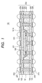
- Fig. 1 is a sectional view for schematically indicating a semiconductor package 100 according to an embodiment 1 of the present invention.
- the semiconductor package 100 according to the embodiment 1 has been schematically manufactured by that a concave portion 101A is formed in a substrate 101 made of silicon, and a semiconductor chip 301 mounted in such a manner that this chip 301 is stored in the concave portion 101A.
- a wiring line structure 200 has been formed in such a manner that on the side of a first major plane (namely, major plane located on opening side of concave portion 101A) and on the side of a second major plane (namely, major plane located on opposite side with respect to opening side of concave portion 101A), the wiring line structure 200 can be externally connected to the semiconductor chip 301.
- a plurality of external connection terminals (bumps) 208 and 210 to be formed on the wiring line structure 200 have been arranged on the first major plane and the second major plane, respectively.
- the above-described external connection terminals 208 and 210 have been arrayed in an array shape as viewed from the plane, namely in a so-termed "full grid array shape.”
- the above-described wiring line structure 200 has been manufactured in accordance with the following feature point: the wiring line structure 200 can be externally connected to the semiconductor chip 301 not only at peripheral portions of the first major plane and the second major plane, but also at least at portions located just above and just under the semiconductor chip 301.
- the above-described wiring line structure 200 has such a structure that while the wiring line structure 200 has via plugs 201 penetrated through the substrate 101, both via plugs and pattern wiring lines for connecting the via plugs 201 to the external terminals 208 and 210 have been formed in/on both planes of the substrate 101, respectively.
- a pattern wiring line 202 which is connected to the via plugs 201 has been formed on the front plane side (namely, side on which semiconductor chip 301 has been mounted) of the substrate 101, and an insulating layer 102 has been formed on this front plane side in such a manner that the insulating layer 102 covers the pattern wiring line 202.
- via plugs 203 have been formed in such a manner that these via plugs 203 penetrate through the insulating layer 102, and a pattern wiring line (electrode pad) 204 which is connected to the via plugs 203 has been formed on the insulating layer 102.
- the external connection terminals (solder bumps) 208 have been formed on the pattern wiring line 204, while the external connection terminals 208 have been arrayed in the full grid array in such a manner that the arrangements of these external connection terminal 208 become the grid shape, as viewed from the plane.
- a connection layer 207 has been formed between the external connection terminals 208 and the pattern wiring line 204.
- the connection layer 207 is made of, for instance, Au/Ni (stacked layer structure made of Au layer and Ni layer in such a manner that Au is located on side of external connection terminals).
- a solder resist layer 103 has been formed around the external connection terminals 208 in such a manner that the solder resist layer 103 covers a portion of the insulating layer 102 and a portion of the pattern wiring line 204.
- an insulating layer 104 has been formed on the side of the rear plane of the substrate 101 (namely, opposite side as to side where semiconductor chip 301 is mounted).
- via plugs 205 which are connected to the via plugs 201 are formed in such a manner that these via plugs 205 penetrate through the insulating layer 104, and also, a pattern wiring line (electrode pad) 206 which is connected to the via plugs 205 has been formed on the insulating layer 104.
- the external connection terminals (solder bumps) 210 have been formed on the pattern wiring line 206, while the external connection terminals 210 have been arrayed in the full grid array in such a manner that the arrangements of these external connection terminal 210 become the grid shape, as viewed from the plane.
- a connection layer 209 has been formed between the external connection terminals 210 and the pattern wiring line 206.
- the connection layer 209 is made of, for instance, Au/Ni (stacked layer structure made of Au layer and Ni layer in such a manner that Au is located on side of external connection terminals).
- a solder resist layer 105 has been formed around the external connection terminals 210 in such a manner that the solder resist layer 105 covers a portion of the insulating layer 104 and a portion of the pattern wiring line 206.
- the insulating layers 102 and 104 are formed of such a material, for example, an epoxy-series resin material is employed as a maj or material which is called as a "build-up" material.
- the wiring line structure 200 (constructed of via plugs 201, 203, 205, and pattern wiring lines 202, 204, 206) is made of, for example, Cu.
- the above-described material is one example, and thus, the present invention is not limited only to these materials.
- the semiconductor chip 301 has been mounted in the concave portion 101A under such a condition that the device plane thereof is directed to a lower direction (bottom plane side of concave portion 101A), namely under a so-called "face down” condition.
- Bumps 302 connected to electrode pads (not shown) formed on the device plane of the semiconductor chip 301 have been connected to the pattern wiring line 202, and an under fill resin (resin material) 303 has been filled between the semiconductor chip 301 and the substrate 101.
- the via plugs 201 which constitute the above-described wiring line structure 200 are formed in a substantially entire plane of the silicon substrate 101 as viewed in the plane, for example, are formed in both such a portion at the bottom portion of the concave portion 101A, the silicon thickness of which is thin, and another portion around the concave portion 101A, the silicon thickness of which is thick.
- the pattern wiring line 202 which is connected to the via plugs 201 and the semiconductor chip 301 has been formed by containing, for example, such a portion which is formed on a side wall surface of the concave portion 101A.
- the pattern wiring line 202 has been connected to both the via plugs 201 and the semiconductor chip 301 (bumps 302) on the bottom plane of the concave portion 101A.
- the pattern wiring line 202 has been formed from the bottom plane of the concave portion 101A to the side wall surface of the concave portion 101A along the inner wall plane of the concave portion 101A, and further, has been formed toward the outer side of the concave portion 101A in such a manner that the pattern wiring line 202 is elongated over the surface of the substrate 101.
- the pattern wiring line 204 which is formed on the insulating layer 101 contains such a portion formed in such a manner that this portion is elongated from a portion which is located outside the concave portion to another portion (located just above semiconductor chip 301) which is overlapped with the concave portion 101A.
- the external connection terminals 208 which are connected to the wiring line structure 200 can be manufactured on the substantially entire plane as to the first major plane, which contains the plane located just above the semiconductor chip 301, in such a manner that these external connection terminals 208 are arranged in the so-called "full grid array.”
- the external connection terminals 210 which are connected to the wiring line structure 200 can be manufactured on the substantially entire plane as to the second major plane, which contains the plane located just under the semiconductor chip 301, in such a manner that these external connection terminals 210 are arranged in the so-called "full grid array.” Further, if necessary, such a pattern wiring line which corresponds to the pattern wiring line 202 and is connected to the via plug 201 may be alternatively provided on the rear plane of the substrate 101.
- the semiconductor package 100 Since the above-described semiconductor package 100 has been constructed in such a manner that the semiconductor chip 301 can be externally connected to the wiring line structure 200 just above and just under this semiconductor chip 301 (for example, has been arranged in full grid array), the semiconductor package 100 can be readily adapted to the multiple pins of the semiconductor chip 301 (namely, total number of bumps 302 is increased).
- a semiconductor package is adapted to a semiconductor chip manufactured with multiple pins, an increasing amount of an area of the semiconductor package can be suppressed and the semiconductor package can have a compact structure. Furthermore, since the above-described semiconductor package is employed, a stacked layer type semiconductor package can be made compact. That is to say, in such a case that the above-described semiconductor packages are stacked with each other, since both planes (namely, first major plane and second major plane) are the full grid array, these semiconductor packages can be connected to each other in a higher efficiency under space saving condition.
- the semiconductor package 100 since the semiconductor chip 301 has been mounted in the concave portion 101A of the silicon substrate 101, the semiconductor package 100 (stacked layer type semiconductor package using semiconductor package 100) can be made slim.
- this semiconductor package 100 can be adapted to such a device having higher performance which is typically known as the semiconductor chip 301 manufactured with the multiple pins, and furthermore, such a stacked layer type semiconductor package capable of accepting both slim and compact requirements (required in mobile appliance etc.) can be constructed.
- the substrate 101 is made of silicon, which may also constitute a feature.
- a semiconductor chip having high performance and multiple pins namely, semiconductor chip 301
- a heat radiation amount thereof is increased.
- both the semiconductor chips 301 formed by employing silicon and the substrate 101 made of silicon have been constituted in such a manner that there is substantially no difference in the thermal expansion coefficients between the semiconductor chip 301 and the substrate 101.
- reliability in the case that a semiconductor chip having high performance which is typically known as a semiconductor chip manufactured with multiple pins is mounted may become superior.
- the wiring line structure 200 is arranged in such a manner that an operation test for the semiconductor chip 301 can be accepted, so that the operation test for the semiconductor chip 301 can also be carried out.
- operation tests for packages are individually carried out with respect to these plural semiconductor chips 301 before these semiconductor packages 100 are stacked with each other. As a result, a manufacturing yield of the resultant stacked layer type semiconductor package can be improved.
- the above-described semiconductor package 100 can be manufactured in accordance with known manufacturing methods (for example, RIE (Reactive Ion Etching) method of silicon, forming of wiring line structure 200 by plating method etc.). Referring now to Fig. 1, manufacturing of the semiconductor package 100 will be schematically and simply explained.
- RIE reactive Ion Etching
- both a structure corresponding to a concave portion 101A and through holes which penetrate through a substrate 101 are firstly formed in the substrate 101 (for example, silicon wafer etc.) made of silicon by an RIE (reactive ion etching) method. Furthermore, after a thermal oxide film (not shown in Fig. 1) has been formed so as to insulate the surface of the substrate 101, via plugs 201 which are made of Cu and are embedded in the through holes are formed by a plating method.
- a pattern wiring line 202 made of Cu is formed by a semi-additive method.
- a pattern wiring line may be alternatively formed also on the rear plane of the substrate 101, if necessary.
- bumps 302 (Au) of a semiconductor chip 301 are joined to the pattern wiring line 202 by applying ultrasonic waves, or by performing a heating method, and then, an under fill resin 303 (fluid resin) is filled between the semiconductor chip 301 and the substrate 101 (flip chip mounting).
- insulating layers 102 and 104 are formed on both planes of the substrate 101 are formed respectively by laminating resin films at a vacuum atmosphere, and then, these formed insulating layers 102 and 104 are heated so as to be hardened. It should be noted that the insulating layers 102 and 104 may be alternatively formed by coating and heating resins. Moreover, after through holes are formed in the insulating layers 102 and 104 (desmear processing is further carried out, if necessary), via plugs 203 and 205, and pattern wiring lines 204 and 206 are formed by the semi-additive method.
- connection layers 207 and 209 are formed respectively on the pattern wiring lines 204 and 206 which are exposed from the solder resist layers 103 and 105 by performing, for example, a plating method, if required.
- external connection terminals 208 and 210 made of solder bumps are formed on the connection layers 207 and 209 (on pattern wiring lines 204 and 206).
- the substrate 101 silicon wafer is diced, so that individual semiconductor packages 100 can be manufactured.
- Fig. 2 is a diagram for showing a stacked layer type package 400 manufactured by employing the semiconductor package 100 formed according to the embodiment 1. It should be noted that the same reference numerals shown in the previous embodiment 1 will be employed as those for denoting the same structural elements, and descriptions thereof will be omitted.
- the stacked layer type semiconductor package 400 has been manufactured by stacking 3 pieces of the above-described semiconductor packages 100 formed according to the embodiment 1 with each other.
- insulating layers UF Under Fill resin
- these insulating layers UF may be omitted.
- the insulating layers UF may be formed by mounting resin films among packages when the packages are stacked with each other.
- an external connection terminal 210 of the semiconductor package 100 located at the lowermost layer has been connected to a mother board S.
- other semiconductor chips, or electronic components such as a capacitor, a resistor, and an inductor may be mounted on a pattern wiring line 204 (connection layer 207) of the semiconductor package 100 located at the uppermost layer.
- the external connection terminal 208 of the semiconductor package 100 provided at the uppermost layer may be omitted from the stacked layer type semiconductor package 400.
- the semiconductor packages 100 manufactured according to the embodiment 1 are employed, it is possible to construct a compact and slim stacked layer type semiconductor package having superior reliability.
- a total number of packages to be stacked with each other is not limited only to 3 pieces.
- a total number of the semiconductor packages 100 to be stacked with each other may be selected to be 2.
- a total quantity of the semiconductor packages 100 to be stacked with each other may be selected to be 4, or more pieces.
- Fig. 3 is a diagram for showing a stacked layer type package 600 manufactured by employing the semiconductor package 100 formed according to the embodiment 1. It should be noted that the same reference numerals shown in the previous embodiment 1 will be employed as those for denoting the same structural elements, and descriptions thereof will be omitted.
- the stacked layer type semiconductor package 600 according to the embodiment 3 has been constructed by stacking a semiconductor package 500 which is different from the semiconductor package 100 on the above-described semiconductor package 100 according to the embodiment 1.
- the above-described semiconductor package 500 has a so-called "F-BGA" structure, namely, such a structure that semiconductor chips 502 and 503 have been stacked on an interposer 501. Further, while the semiconductor chips 502 and 503 have been electrically connected to the interposer 501 by wires 504 and 505 respectively, these semiconductor chips 502 and 503 have been sealed on the interposer 501 by a molding resin 506.
- the above-explained structure may be changed into another structure in which the semiconductor chip 502 is flip-chip-connected to the interposer 501, and the semiconductor chip 503 mounted on a rear plane (upper plane) of the semiconductor chip 502 is connected to the interposer 501 by a wire.
- a plurality of semiconductor chips for instance, stacked type semiconductor chips
- a plurality of concave portions 101A may be alternatively formed in the substrate 101, a plurality of semiconductor chips may be alternatively mounted.
- a stacked layer type semiconductor package constructed by stacking a plurality of packages with each other, the plurality of packages include a semiconductor package including: a semiconductor chip; a substrate in which a concave portion has been formed, the semiconductor chip being mounted in the concave portion; and a wiring line structure constructed in such a manner that the wiring line structure can be externally connected to the semiconductor chip at least just above and just under the semiconductor chip.
- the semiconductor package having superior reliability which is made compact and slim
- the stacked layer type semiconductor package having superior reliability which is made compact and slim
Landscapes
- Production Of Multi-Layered Print Wiring Board (AREA)
- Wire Bonding (AREA)
- Structures Or Materials For Encapsulating Or Coating Semiconductor Devices Or Solid State Devices (AREA)
- Internal Circuitry In Semiconductor Integrated Circuit Devices (AREA)
Abstract
Description
- The present invention generally relates to a semiconductor package. In particular the present invention is related to a semiconductor package constructed by mounting a semiconductor chip on a substrate, and a stacked layer type semiconductor package with employment of the above-described semiconductor package. More specifically, it relates to a semiconductor package and a stacked layer type semiconductor package.
- While various types of structures of packages for semiconductor chips have been proposed, since electronic appliances on which packages are mounted are manufactured with high performance, there are some cases that, for instance, stacked layer type packages (will also be referred to as "package-on-package (PoP)") made by stacking conventional packages with each other are employed.
- While stacked layer type packages have such structures constructed in such a manner that plural pieces of packages containing semiconductor chips are stacked on each other, since various types of packages can be combined with each other, these stacked layer type packages can be easily adapted to high-performance electronic appliances manufactured in various specifications.
- For example, see
JP-A-2005-347229 - However, among current semiconductor chips, total numbers of connection terminals are increased in connection with high performance of these semiconductor chips, namely, a so-called "multiple pin" of semiconductor chips have been popularized. When packages are constructed which can be adapted to semiconductor chips manufactured with the above-described "multiple pins", total numbers of connection terminals employed in these packages are increased. As a result, there is such a problem that these packages can be hardly stacked with each other.
- For example, when packages manufactured with so-called "multiple pins" are stacked with each other, areas used to electrically connect these packages with each other must be secured. As a result, there is another problem that stacked layer type packages become bulky. Further, since there is such a problem that thickness of the stacked layer type packages are increased, there is a further problem that these stacked layer packages can be hardly made thicker. As previously described, no concrete structural example has been proposed as to such stacked layer type packages capable of being adapted to the "multiple pins" and also capable of being made compact.
- Further, in the above-described semiconductor chips having high performance and manufactured with the multiple pins, since heat generation amounts of the semiconductor chips are increased, there are some possibilities that various package failures may occur due to thermal cycles of the semiconductor chips.
- For instance, general-purpose semiconductor chips are manufactured by silicon. As a result, there is a large difference in thermal expansion coefficients between the silicon and interposers. The interposers are made of resin materials employed in general-purpose packages.
- As a consequence, when heat radiation and heat dissipation of the semiconductor chips are repeatedly performed, there is a risk that wire disconnections of packages occur and the packages are broken due to differences in the thermal expansion coefficients between the semiconductor chips and the interposers. Thus, there is another problem that reliability of these packages is lowered.
- In light of the above, a semiconductor package according to independent claim 1, and a stacked layer type semiconductor package according to claim 5 are provided.
- Further advantages, features, aspects and details are evident from the dependent claims, the description and the drawings.
- As a consequence, the present invention has a unified object to provide a semiconductor package and a stacked layer type semiconductor package, which can solve the above-described problems, and are novel and useful.
- A concrete object of the present invention is to provide both a semiconductor package having superior reliability, which is made compact and slim, and also a stacked layer type semiconductor package having superior reliability, which is made compact and slim.
- According to a first aspect of the present invention, the above-described problems are solved by a semiconductor package featured including:
- a semiconductor chip;
- a substrate provided with a concave portion in which the semiconductor chip is mounted; and
- a wiring line structure constructed in such a manner that the wiring line structure can be externally connected to the semiconductor chip at least just above and just under the semiconductor chip.
- Further, according to a second aspect of the present invention, the above-described problems are solved by such a stacked layer type semiconductor package constructed by stacking a plurality of packages with each other, wherein
the plurality of packages which is a semiconductor package, including: - a semiconductor chip;
- a substrate provided with a concave portion in which the semiconductor chip is mounted; and
- a wiring line structure constructed in such a manner that the wiring line structure can be externally connected to the semiconductor chip at least just above and just under the semiconductor chip.
- In accordance with the present invention, it is possible to provide the semiconductor package having superior reliability, which is made compact and slim, and also the stacked layer type semiconductor package having superior reliability, which is made compact and slim.
- The invention will be better understood by reference to the following description of embodiments of the invention taken in conjunction with the accompanying drawings, wherein:
- Fig. 1 is a diagram for indicating a semiconductor package according to an embodiment 1.
- Fig. 2 is a diagram for showing a stacked layer type semiconductor package according to an embodiment 2.
- Fig. 3 is a diagram for showing a stacked layer type semiconductor package according to an embodiment 3.
- A semiconductor package, according to the present invention, is featured by including: a semiconductor chip; a substrate in which a concave portion has been formed, the semiconductor chip being mounted in the concave portion; and a wiring line structure constructed in such a manner that the wiring line structure can be externally connected to the semiconductor chip at least just above and just under the semiconductor chip.
- In the above-described semiconductor package, the wiring line structure can be externally connected to the semiconductor chip at least at positions located just above and just under the semiconductor chip (external connection terminal is provided). For example, in the above-described semiconductor package, connection terminals can be arranged on both a first major plane and a second major plane in a so-called "full grid array" form. As a result, if the above-described semiconductor package is employed, then a stacked layer type semiconductor package can be made compact. Further, since the semiconductor chip has been mounted in the concave portion of the silicon substrate in the above-described semiconductor chip, a semiconductor package (stacked layer type semiconductor package) can be made slim.
- In other words, since the above-described semiconductor package is employed, such a stacked layer type semiconductor package can be constructed in a compact and slim size, and can be adapted to a device having high performance (typically known as semiconductor chip having multiple pins) and also a mobile appliance.
- Further, in the above-described semiconductor package, a silicon substrate may be preferably employed as the substrate in which the concave portion for mounting the semiconductor chip has been formed. For example, as to the previously explained semiconductor chip having high performance, there are some cases that a heat radiation amount thereof is increased. As a result, in such a package with employment of a substrate (interposer) made of the conventional resin material, there is such a risk that problems may occur, namely, wiring lines of the package are disconnected, or are damaged due to a difference in thermal expansion coefficients between silicon for constructing the semiconductor chip and the resin material for constructing the substrate.
- On the other hand, in the above-described semiconductor package according to the present invention, since there is substantially no difference in thermal expansion coefficients between the semiconductor chip and the substrate, there is such an advantage that reliability can become superior in such a case that a semiconductor chip having high performance is mounted which is typically known as a semiconductor chip equipped with multiple pins.
- Further, as the material for constructing the above-described substrate, for example, glass and ceramics may be alternatively employed. For instance, since compositions of glass and ceramics are adjusted, thermal expansion coefficients thereof may be approximated to that of the semiconductor chip (silicon)
- Next, a concrete description is made of a structural example with respect to the above-explained semiconductor package and the above-explained stacked layer type semiconductor package using the semiconductor package with reference to drawings.
- Fig. 1 is a sectional view for schematically indicating a
semiconductor package 100 according to an embodiment 1 of the present invention. Referring now to Fig. 1, thesemiconductor package 100 according to the embodiment 1 has been schematically manufactured by that aconcave portion 101A is formed in asubstrate 101 made of silicon, and asemiconductor chip 301 mounted in such a manner that thischip 301 is stored in theconcave portion 101A. - Further, in the
semiconductor package 100, awiring line structure 200 has been formed in such a manner that on the side of a first major plane (namely, major plane located on opening side ofconcave portion 101A) and on the side of a second major plane (namely, major plane located on opposite side with respect to opening side ofconcave portion 101A), thewiring line structure 200 can be externally connected to thesemiconductor chip 301. For example, a plurality of external connection terminals (bumps) 208 and 210 to be formed on thewiring line structure 200 have been arranged on the first major plane and the second major plane, respectively. - The above-described
external connection terminals wiring line structure 200 has been manufactured in accordance with the following feature point: thewiring line structure 200 can be externally connected to thesemiconductor chip 301 not only at peripheral portions of the first major plane and the second major plane, but also at least at portions located just above and just under thesemiconductor chip 301. - For instance, the above-described
wiring line structure 200 has such a structure that while thewiring line structure 200 has viaplugs 201 penetrated through thesubstrate 101, both via plugs and pattern wiring lines for connecting the viaplugs 201 to theexternal terminals substrate 101, respectively. - For instance, a
pattern wiring line 202 which is connected to thevia plugs 201 has been formed on the front plane side (namely, side on whichsemiconductor chip 301 has been mounted) of thesubstrate 101, and aninsulating layer 102 has been formed on this front plane side in such a manner that theinsulating layer 102 covers thepattern wiring line 202. Furthermore, viaplugs 203 have been formed in such a manner that these viaplugs 203 penetrate through theinsulating layer 102, and a pattern wiring line (electrode pad) 204 which is connected to thevia plugs 203 has been formed on theinsulating layer 102. - Further, the external connection terminals (solder bumps) 208 have been formed on the
pattern wiring line 204, while theexternal connection terminals 208 have been arrayed in the full grid array in such a manner that the arrangements of theseexternal connection terminal 208 become the grid shape, as viewed from the plane. Further, if necessary, aconnection layer 207 has been formed between theexternal connection terminals 208 and thepattern wiring line 204. Theconnection layer 207 is made of, for instance, Au/Ni (stacked layer structure made of Au layer and Ni layer in such a manner that Au is located on side of external connection terminals). Moreover, asolder resist layer 103 has been formed around theexternal connection terminals 208 in such a manner that thesolder resist layer 103 covers a portion of theinsulating layer 102 and a portion of thepattern wiring line 204. - Further, an
insulating layer 104 has been formed on the side of the rear plane of the substrate 101 (namely, opposite side as to side wheresemiconductor chip 301 is mounted). In addition, viaplugs 205 which are connected to thevia plugs 201 are formed in such a manner that these viaplugs 205 penetrate through theinsulating layer 104, and also, a pattern wiring line (electrode pad) 206 which is connected to thevia plugs 205 has been formed on theinsulating layer 104. - Further, as previously described, the external connection terminals (solder bumps) 210 have been formed on the
pattern wiring line 206, while theexternal connection terminals 210 have been arrayed in the full grid array in such a manner that the arrangements of theseexternal connection terminal 210 become the grid shape, as viewed from the plane. Further, if necessary, aconnection layer 209 has been formed between theexternal connection terminals 210 and thepattern wiring line 206. Theconnection layer 209 is made of, for instance, Au/Ni (stacked layer structure made of Au layer and Ni layer in such a manner that Au is located on side of external connection terminals). Moreover, a solder resistlayer 105 has been formed around theexternal connection terminals 210 in such a manner that the solder resistlayer 105 covers a portion of the insulatinglayer 104 and a portion of thepattern wiring line 206. - In the above-described structure, the insulating
layers plugs pattern wiring lines - The
semiconductor chip 301 has been mounted in theconcave portion 101A under such a condition that the device plane thereof is directed to a lower direction (bottom plane side ofconcave portion 101A), namely under a so-called "face down" condition.Bumps 302 connected to electrode pads (not shown) formed on the device plane of thesemiconductor chip 301 have been connected to thepattern wiring line 202, and an under fill resin (resin material) 303 has been filled between thesemiconductor chip 301 and thesubstrate 101. - The via plugs 201 which constitute the above-described
wiring line structure 200 are formed in a substantially entire plane of thesilicon substrate 101 as viewed in the plane, for example, are formed in both such a portion at the bottom portion of theconcave portion 101A, the silicon thickness of which is thin, and another portion around theconcave portion 101A, the silicon thickness of which is thick. - Further, the
pattern wiring line 202 which is connected to the via plugs 201 and the semiconductor chip 301 (bumps 302) has been formed by containing, for example, such a portion which is formed on a side wall surface of theconcave portion 101A. For instance, thepattern wiring line 202 has been connected to both the via plugs 201 and the semiconductor chip 301 (bumps 302) on the bottom plane of theconcave portion 101A. Further, thepattern wiring line 202 has been formed from the bottom plane of theconcave portion 101A to the side wall surface of theconcave portion 101A along the inner wall plane of theconcave portion 101A, and further, has been formed toward the outer side of theconcave portion 101A in such a manner that thepattern wiring line 202 is elongated over the surface of thesubstrate 101. - On the other hand, the
pattern wiring line 204 which is formed on the insulatinglayer 101 contains such a portion formed in such a manner that this portion is elongated from a portion which is located outside the concave portion to another portion (located just above semiconductor chip 301) which is overlapped with theconcave portion 101A. - Since the
wiring line structure 200 has been formed in the above-described manner, theexternal connection terminals 208 which are connected to thewiring line structure 200 can be manufactured on the substantially entire plane as to the first major plane, which contains the plane located just above thesemiconductor chip 301, in such a manner that theseexternal connection terminals 208 are arranged in the so-called "full grid array." - Further, in the above-described
semiconductor package 100, theexternal connection terminals 210 which are connected to thewiring line structure 200 can be manufactured on the substantially entire plane as to the second major plane, which contains the plane located just under thesemiconductor chip 301, in such a manner that theseexternal connection terminals 210 are arranged in the so-called "full grid array." Further, if necessary, such a pattern wiring line which corresponds to thepattern wiring line 202 and is connected to the viaplug 201 may be alternatively provided on the rear plane of thesubstrate 101. - Since the above-described
semiconductor package 100 has been constructed in such a manner that thesemiconductor chip 301 can be externally connected to thewiring line structure 200 just above and just under this semiconductor chip 301 (for example, has been arranged in full grid array), thesemiconductor package 100 can be readily adapted to the multiple pins of the semiconductor chip 301 (namely, total number ofbumps 302 is increased). - As a consequence, even in such a case that a semiconductor package is adapted to a semiconductor chip manufactured with multiple pins, an increasing amount of an area of the semiconductor package can be suppressed and the semiconductor package can have a compact structure. Furthermore, since the above-described semiconductor package is employed, a stacked layer type semiconductor package can be made compact. That is to say, in such a case that the above-described semiconductor packages are stacked with each other, since both planes (namely, first major plane and second major plane) are the full grid array, these semiconductor packages can be connected to each other in a higher efficiency under space saving condition.
- Further, in the above-described
semiconductor package 100, since thesemiconductor chip 301 has been mounted in theconcave portion 101A of thesilicon substrate 101, the semiconductor package 100 (stacked layer type semiconductor package using semiconductor package 100) can be made slim. - In other words, since the above-described
semiconductor package 100 is employed, thissemiconductor package 100 can be adapted to such a device having higher performance which is typically known as thesemiconductor chip 301 manufactured with the multiple pins, and furthermore, such a stacked layer type semiconductor package capable of accepting both slim and compact requirements (required in mobile appliance etc.) can be constructed. - Further, in the above-described
semiconductor package 100, thesubstrate 101 is made of silicon, which may also constitute a feature. For instance, there are some cases that in a semiconductor chip having high performance and multiple pins (namely, semiconductor chip 301), a heat radiation amount thereof is increased. In order to solve such a large heat radiation problem, in the above-describedsemiconductor package 100, both thesemiconductor chips 301 formed by employing silicon and thesubstrate 101 made of silicon have been constituted in such a manner that there is substantially no difference in the thermal expansion coefficients between thesemiconductor chip 301 and thesubstrate 101. As a consequence, reliability in the case that a semiconductor chip having high performance which is typically known as a semiconductor chip manufactured with multiple pins is mounted may become superior. - Further, in the above-explained
semiconductor package 100, thewiring line structure 200 is arranged in such a manner that an operation test for thesemiconductor chip 301 can be accepted, so that the operation test for thesemiconductor chip 301 can also be carried out. For example, in the case that a plurality of the semiconductor packages 100 are stacked with each other so as to construct a stacked layer type semiconductor package, operation tests for packages are individually carried out with respect to theseplural semiconductor chips 301 before thesesemiconductor packages 100 are stacked with each other. As a result, a manufacturing yield of the resultant stacked layer type semiconductor package can be improved. - The above-described
semiconductor package 100 can be manufactured in accordance with known manufacturing methods (for example, RIE (Reactive Ion Etching) method of silicon, forming ofwiring line structure 200 by plating method etc.). Referring now to Fig. 1, manufacturing of thesemiconductor package 100 will be schematically and simply explained. - In such a case that the above-described
semiconductor package 100 is manufactured, both a structure corresponding to aconcave portion 101A and through holes which penetrate through asubstrate 101 are firstly formed in the substrate 101 (for example, silicon wafer etc.) made of silicon by an RIE (reactive ion etching) method. Furthermore, after a thermal oxide film (not shown in Fig. 1) has been formed so as to insulate the surface of thesubstrate 101, viaplugs 201 which are made of Cu and are embedded in the through holes are formed by a plating method. - Next, a
pattern wiring line 202 made of Cu is formed by a semi-additive method. In this case, a pattern wiring line may be alternatively formed also on the rear plane of thesubstrate 101, if necessary. Subsequently, bumps 302 (Au) of asemiconductor chip 301 are joined to thepattern wiring line 202 by applying ultrasonic waves, or by performing a heating method, and then, an under fill resin 303 (fluid resin) is filled between thesemiconductor chip 301 and the substrate 101 (flip chip mounting). - Next, insulating
layers substrate 101 are formed respectively by laminating resin films at a vacuum atmosphere, and then, these formed insulatinglayers layers layers 102 and 104 (desmear processing is further carried out, if necessary), viaplugs pattern wiring lines - Next, after solder resist
layers pattern wiring lines layers external connection terminals pattern wiring lines 204 and 206). Thereafter, the substrate 101 (silicon wafer) is diced, so thatindividual semiconductor packages 100 can be manufactured. - Fig. 2 is a diagram for showing a stacked
layer type package 400 manufactured by employing thesemiconductor package 100 formed according to the embodiment 1. It should be noted that the same reference numerals shown in the previous embodiment 1 will be employed as those for denoting the same structural elements, and descriptions thereof will be omitted. - Referring now to Fig. 2, the stacked layer
type semiconductor package 400, according to this embodiment 2 of the present invention, has been manufactured by stacking 3 pieces of the above-describedsemiconductor packages 100 formed according to the embodiment 1 with each other. Although insulating layers UF (Under Fill resin) have been formed among the semiconductor packages 100 to be stacked each other, into which fluid resins have been filled and hardened, these insulating layers UF may be omitted. Alternatively, the insulating layers UF may be formed by mounting resin films among packages when the packages are stacked with each other. - In the above-described structure, an
external connection terminal 210 of thesemiconductor package 100 located at the lowermost layer has been connected to a mother board S. Further, for example, other semiconductor chips, or electronic components (surface packaging components) such as a capacitor, a resistor, and an inductor may be mounted on a pattern wiring line 204 (connection layer 207) of thesemiconductor package 100 located at the uppermost layer. Further, theexternal connection terminal 208 of thesemiconductor package 100 provided at the uppermost layer may be omitted from the stacked layertype semiconductor package 400. - As previously described, since the semiconductor packages 100 manufactured according to the embodiment 1 are employed, it is possible to construct a compact and slim stacked layer type semiconductor package having superior reliability.
- Further, a total number of packages to be stacked with each other is not limited only to 3 pieces. For example, a total number of the semiconductor packages 100 to be stacked with each other may be selected to be 2. Alternatively, a total quantity of the semiconductor packages 100 to be stacked with each other may be selected to be 4, or more pieces.
- Fig. 3 is a diagram for showing a stacked
layer type package 600 manufactured by employing thesemiconductor package 100 formed according to the embodiment 1. It should be noted that the same reference numerals shown in the previous embodiment 1 will be employed as those for denoting the same structural elements, and descriptions thereof will be omitted. - Referring to Fig. 3, the stacked layer
type semiconductor package 600 according to the embodiment 3 has been constructed by stacking asemiconductor package 500 which is different from thesemiconductor package 100 on the above-describedsemiconductor package 100 according to the embodiment 1. - The above-described
semiconductor package 500 has a so-called "F-BGA" structure, namely, such a structure thatsemiconductor chips interposer 501. Further, while thesemiconductor chips interposer 501 bywires semiconductor chips interposer 501 by amolding resin 506. - Alternatively, the above-explained structure may be changed into another structure in which the
semiconductor chip 502 is flip-chip-connected to theinterposer 501, and thesemiconductor chip 503 mounted on a rear plane (upper plane) of thesemiconductor chip 502 is connected to theinterposer 501 by a wire. - As previously described, as a package which is stacked on the
semiconductor package 100 according to the embodiment 1, such package having various structures and various arrangements may be selected. - While the present invention has been described with reference to the preferred embodiments, the present invention is not limited only to the above-described specific embodiments, but may be modified and changed in various manners within the gist described in the scope of claims.
- For example, a plurality of semiconductor chips (for instance, stacked type semiconductor chips) to be mounted in the
concave portion 101A may be alternatively employed. Further, while a plurality ofconcave portions 101A may be alternatively formed in thesubstrate 101, a plurality of semiconductor chips may be alternatively mounted. - According to embodiments described herein, it can be provided in a stacked layer type semiconductor package constructed by stacking a plurality of packages with each other, the plurality of packages include a semiconductor package including: a semiconductor chip; a substrate in which a concave portion has been formed, the semiconductor chip being mounted in the concave portion; and a wiring line structure constructed in such a manner that the wiring line structure can be externally connected to the semiconductor chip at least just above and just under the semiconductor chip.
- In accordance with the present invention, it is possible to provide the semiconductor package having superior reliability, which is made compact and slim, and also the stacked layer type semiconductor package having superior reliability, which is made compact and slim.
Claims (5)
- A semiconductor package (100) comprising:a semiconductor chip (301);a substrate provided with a concave portion (101A) in which the semiconductor chip is mounted; anda wiring line structure (200) constructed in such a manner that the wiring line structure can be externally connected to the semiconductor chip at least just above and just under the semiconductor chip.
- The semiconductor package as claimed in claim 1, wherein
the semiconductor chip (301) is mounted in the concave portion under face down condition. - The semiconductor package as claimed in any of claims 1 to 2, wherein
the wiring line structure contains a via plug (201) which penetrates through a bottom portion of the concave portion of the substrate. - The semiconductor package as claimed in claim 3, wherein
the wiring line structure (200) has a pattern wiring line (202) which contains a portion formed on a side wall surface of the concave portion (101A). - A stacked layer type semiconductor package (400; 600) constructed by stacking a plurality of packages (100) with each other, wherein
the plurality of packages which is a semiconductor package (100) according to any of claims 1 to 4.
Applications Claiming Priority (1)
| Application Number | Priority Date | Filing Date | Title |
|---|---|---|---|
| JP2006292820A JP5042591B2 (en) | 2006-10-27 | 2006-10-27 | Semiconductor package and stacked semiconductor package |
Publications (2)
| Publication Number | Publication Date |
|---|---|
| EP1916713A2 true EP1916713A2 (en) | 2008-04-30 |
| EP1916713A3 EP1916713A3 (en) | 2010-01-27 |
Family
ID=39106100
Family Applications (1)
| Application Number | Title | Priority Date | Filing Date |
|---|---|---|---|
| EP07021111A Withdrawn EP1916713A3 (en) | 2006-10-27 | 2007-10-29 | Semiconductor package and stacked layer type semiconductor package formed with it |
Country Status (6)
| Country | Link |
|---|---|
| US (1) | US8253229B2 (en) |
| EP (1) | EP1916713A3 (en) |
| JP (1) | JP5042591B2 (en) |
| KR (1) | KR101412718B1 (en) |
| CN (1) | CN101170095B (en) |
| TW (1) | TW200820417A (en) |
Families Citing this family (47)
| Publication number | Priority date | Publication date | Assignee | Title |
|---|---|---|---|---|
| US8118950B2 (en) * | 2007-12-04 | 2012-02-21 | Alcoa Inc. | Aluminum-copper-lithium alloys |
| US8618669B2 (en) * | 2008-01-09 | 2013-12-31 | Ibiden Co., Ltd. | Combination substrate |
| US8378475B1 (en) * | 2008-05-30 | 2013-02-19 | Wavefront Research, Inc. | Optoelectronic chip carriers |
| CN101872749B (en) * | 2009-04-24 | 2012-05-23 | 南茂科技股份有限公司 | Recess chip packaging structure and laminated packaging structure using same |
| CN101872757B (en) * | 2009-04-24 | 2012-05-23 | 南茂科技股份有限公司 | Recess chip packaging structure and laminated packaging structure using same |
| US8310835B2 (en) * | 2009-07-14 | 2012-11-13 | Apple Inc. | Systems and methods for providing vias through a modular component |
| US8895358B2 (en) * | 2009-09-11 | 2014-11-25 | Stats Chippac, Ltd. | Semiconductor device and method of forming cavity in PCB containing encapsulant or dummy die having CTE similar to CTE of large array WLCSP |
| KR101046713B1 (en) * | 2009-12-17 | 2011-07-06 | 삼성전기주식회사 | Package Substrate and Manufacturing Method of Package Substrate |
| KR101676620B1 (en) * | 2010-02-05 | 2016-11-16 | 에스케이하이닉스 주식회사 | Stacked semiconductor package |
| JP5218460B2 (en) | 2010-03-26 | 2013-06-26 | セイコーエプソン株式会社 | Pyroelectric detector, pyroelectric detector and electronic device |
| CN102215043A (en) * | 2010-04-09 | 2011-10-12 | 国民技术股份有限公司 | Wireless communication module |
| JP5517800B2 (en) * | 2010-07-09 | 2014-06-11 | キヤノン株式会社 | Member for solid-state imaging device and method for manufacturing solid-state imaging device |
| US8847376B2 (en) * | 2010-07-23 | 2014-09-30 | Tessera, Inc. | Microelectronic elements with post-assembly planarization |
| CN102403275B (en) * | 2010-09-17 | 2014-01-15 | 深南电路有限公司 | Package on package structure and fabricating method for same |
| CN102064159B (en) * | 2010-11-05 | 2013-09-18 | 中国兵器工业集团第二一四研究所苏州研发中心 | Multi-module packaged component |
| JP5357241B2 (en) * | 2011-08-10 | 2013-12-04 | 新光電気工業株式会社 | Semiconductor device and manufacturing method of semiconductor device |
| WO2013070207A1 (en) * | 2011-11-09 | 2013-05-16 | Intel Corporation | Thermal expansion compensators for controlling microelectronic package warpage |
| US8749043B2 (en) | 2012-03-01 | 2014-06-10 | Taiwan Semiconductor Manufacturing Company, Ltd. | Package on package structure |
| CN103811444B (en) * | 2012-11-07 | 2016-11-23 | 环旭电子股份有限公司 | The manufacture method of electronic installation, system-in-package module and system-in-package module |
| US9627325B2 (en) * | 2013-03-06 | 2017-04-18 | Taiwan Semiconductor Manufacturing Company, Ltd. | Package alignment structure and method of forming same |
| JP2014209091A (en) * | 2013-03-25 | 2014-11-06 | ローム株式会社 | Semiconductor device |
| CN103390717B (en) * | 2013-07-30 | 2016-02-03 | 广东洲明节能科技有限公司 | Lamination LED illuminating module and manufacture method |
| CN103579206B (en) * | 2013-11-07 | 2016-09-21 | 华进半导体封装先导技术研发中心有限公司 | Stack packaged device and manufacture method thereof |
| JP5958454B2 (en) * | 2013-12-05 | 2016-08-02 | 株式会社村田製作所 | Built-in module |
| TW201526198A (en) * | 2013-12-18 | 2015-07-01 | 標準科技股份有限公司 | Package module with stacked components |
| DE102014206608A1 (en) | 2014-04-04 | 2015-10-08 | Siemens Aktiengesellschaft | A method of mounting an electrical component using a hood and a hood suitable for use in this method |
| DE102014206601A1 (en) * | 2014-04-04 | 2015-10-08 | Siemens Aktiengesellschaft | A method of mounting an electrical component using a hood and a hood suitable for use in this method |
| KR101565690B1 (en) * | 2014-04-10 | 2015-11-03 | 삼성전기주식회사 | Circuit board, method for menufacturing of circuit board, electronic component package and method for menufacturing of electronic component package |
| KR102262907B1 (en) * | 2014-05-30 | 2021-06-09 | 삼성전기주식회사 | Package substrate, package, package on package and maunfacutring method of package substrate |
| JP6554338B2 (en) * | 2014-07-28 | 2019-07-31 | ローム株式会社 | Semiconductor device |
| TWI571185B (en) * | 2014-10-15 | 2017-02-11 | 矽品精密工業股份有限公司 | Electronic package and its manufacturing method |
| JP6606331B2 (en) * | 2015-02-16 | 2019-11-13 | ローム株式会社 | Electronic equipment |
| JP6557481B2 (en) * | 2015-02-26 | 2019-08-07 | ローム株式会社 | Electronic equipment |
| JP6676308B2 (en) * | 2015-08-07 | 2020-04-08 | ローム株式会社 | Semiconductor device |
| JP2017037900A (en) * | 2015-08-07 | 2017-02-16 | ローム株式会社 | Semiconductor device and manufacturing method thereof |
| CN105118815B (en) * | 2015-08-13 | 2017-09-29 | 上海航天电子通讯设备研究所 | A kind of three-dimension packaging vertical interconnecting structure based on aluminium base and preparation method thereof |
| CN105489589B (en) * | 2016-01-26 | 2018-06-01 | 兰微悦美(北京)科技有限公司 | Stackable integrated circuit and its method for packing |
| JP2017175000A (en) * | 2016-03-24 | 2017-09-28 | ローム株式会社 | Electronic component, manufacturing method thereof, and interposer |
| JP6770331B2 (en) * | 2016-05-02 | 2020-10-14 | ローム株式会社 | Electronic components and their manufacturing methods |
| US10497846B2 (en) * | 2017-07-11 | 2019-12-03 | Lg Innotek Co., Ltd. | Light emitting device package |
| KR102448248B1 (en) * | 2018-05-24 | 2022-09-27 | 삼성전자주식회사 | Package-on-package type semiconductor package and method for fabricating the same |
| US11309285B2 (en) * | 2019-06-13 | 2022-04-19 | Micron Technology, Inc. | Three-dimensional stacking semiconductor assemblies and methods of manufacturing the same |
| KR102785840B1 (en) * | 2019-12-13 | 2025-03-26 | 삼성전자주식회사 | Semiconductor package |
| CN111446215A (en) * | 2020-05-11 | 2020-07-24 | 苏州融睿电子科技有限公司 | Packaging structure, method and packaging device of packaging device |
| US20220254945A1 (en) * | 2021-02-08 | 2022-08-11 | The Hong Kong University Of Science And Technology | Low-power photonic demodulator |
| US12399334B2 (en) * | 2021-09-22 | 2025-08-26 | Intel Corporation | Photonic integrated circuit packaging architectures |
| US12392970B2 (en) | 2021-09-22 | 2025-08-19 | Intel Corporation | Photonic integrated circuit packaging architectures |
Family Cites Families (26)
| Publication number | Priority date | Publication date | Assignee | Title |
|---|---|---|---|---|
| DE69633324T2 (en) * | 1995-06-06 | 2005-09-15 | The Chamberlain Group, Inc., Elmhurst | MOVABLE BARRIER OPERATING DEVICE WITH LEARNING FOR POWER AND POSITION |
| JPH11168150A (en) * | 1997-12-04 | 1999-06-22 | Mitsubishi Electric Corp | Semiconductor integrated circuit device |
| JPH11289023A (en) | 1998-04-02 | 1999-10-19 | Oki Electric Ind Co Ltd | Semiconductor device and manufacturing method thereof |
| TW388201B (en) * | 1998-04-22 | 2000-04-21 | World Wiser Electronics Inc | Method for producing thermal structure of printed circuit board |
| KR100266693B1 (en) * | 1998-05-30 | 2000-09-15 | 김영환 | Stackable ball grid array semiconductor package and fabrication method thereof |
| TW399309B (en) * | 1998-09-30 | 2000-07-21 | World Wiser Electronics Inc | Cavity-down package structure with thermal via |
| JP2001230515A (en) * | 2000-02-15 | 2001-08-24 | Matsushita Electric Ind Co Ltd | Electronic component mounted body, electronic component mounted body manufacturing method, and secondary mounted structure of mounted body. |
| WO2001063991A1 (en) | 2000-02-25 | 2001-08-30 | Ibiden Co., Ltd. | Multilayer printed wiring board and method for producing multilayer printed wiring board |
| JP2001274324A (en) * | 2000-03-24 | 2001-10-05 | Hitachi Chem Co Ltd | Semiconductor mounting substrate for stacked semiconductor device, semiconductor device, and stacked semiconductor device |
| CN1543298A (en) * | 2000-06-27 | 2004-11-03 | ���µ�����ҵ��ʽ���� | Ceramic laminated device |
| JP2002026187A (en) * | 2000-07-07 | 2002-01-25 | Sony Corp | Semiconductor package and method of manufacturing semiconductor package |
| US20020020898A1 (en) * | 2000-08-16 | 2002-02-21 | Vu Quat T. | Microelectronic substrates with integrated devices |
| EP1400820A1 (en) * | 2002-09-20 | 2004-03-24 | Corning O.T.I. SRL | Integrated optical chip |
| WO2004047167A1 (en) * | 2002-11-21 | 2004-06-03 | Nec Corporation | Semiconductor device, wiring substrate, and method for manufacturing wiring substrate |
| JP4137659B2 (en) * | 2003-02-13 | 2008-08-20 | 新光電気工業株式会社 | Electronic component mounting structure and manufacturing method thereof |
| KR20040078807A (en) * | 2003-03-05 | 2004-09-13 | 삼성전자주식회사 | Ball Grid Array Stack Package |
| US7070207B2 (en) * | 2003-04-22 | 2006-07-04 | Ibiden Co., Ltd. | Substrate for mounting IC chip, multilayerd printed circuit board, and device for optical communication |
| JP2004363351A (en) * | 2003-06-05 | 2004-12-24 | Mitsubishi Electric Corp | Stacked semiconductor device |
| JP4298559B2 (en) * | 2004-03-29 | 2009-07-22 | 新光電気工業株式会社 | Electronic component mounting structure and manufacturing method thereof |
| JP2005347299A (en) * | 2004-05-31 | 2005-12-15 | Shinko Electric Ind Co Ltd | Manufacturing method of chip embedded substrate |
| JP2005347229A (en) | 2004-06-04 | 2005-12-15 | Teruo Kamagata | Remote controlled luminaire of no need for dedicated remote control |
| KR100673354B1 (en) * | 2004-06-18 | 2007-01-24 | 주식회사 네패스 | Semiconductor imaging device package and manufacturing method thereof |
| DE602004016483D1 (en) * | 2004-07-16 | 2008-10-23 | St Microelectronics Sa | Electronic circuit arrangement, apparatus with such an arrangement and manufacturing method |
| KR100669830B1 (en) * | 2004-11-16 | 2007-04-16 | 삼성전자주식회사 | Multilayer Package Using Anisotropic Conductive Film |
| KR100618892B1 (en) * | 2005-04-13 | 2006-09-01 | 삼성전자주식회사 | Semiconductor package achieves fan-out structure through wire bonding |
| JP2006351565A (en) | 2005-06-13 | 2006-12-28 | Shinko Electric Ind Co Ltd | Stacked semiconductor package |
-
2006
- 2006-10-27 JP JP2006292820A patent/JP5042591B2/en active Active
-
2007
- 2007-10-23 US US11/976,249 patent/US8253229B2/en active Active
- 2007-10-25 KR KR1020070107806A patent/KR101412718B1/en active Active
- 2007-10-26 CN CN200710163745XA patent/CN101170095B/en active Active
- 2007-10-26 TW TW096140212A patent/TW200820417A/en unknown
- 2007-10-29 EP EP07021111A patent/EP1916713A3/en not_active Withdrawn
Also Published As
| Publication number | Publication date |
|---|---|
| CN101170095B (en) | 2010-11-10 |
| JP5042591B2 (en) | 2012-10-03 |
| US20080290491A1 (en) | 2008-11-27 |
| TW200820417A (en) | 2008-05-01 |
| EP1916713A3 (en) | 2010-01-27 |
| JP2008109046A (en) | 2008-05-08 |
| CN101170095A (en) | 2008-04-30 |
| KR20080038035A (en) | 2008-05-02 |
| US8253229B2 (en) | 2012-08-28 |
| KR101412718B1 (en) | 2014-06-27 |
Similar Documents
| Publication | Publication Date | Title |
|---|---|---|
| US8253229B2 (en) | Semiconductor package and stacked layer type semiconductor package | |
| US6558978B1 (en) | Chip-over-chip integrated circuit package | |
| KR101461630B1 (en) | Wafer level chip on chip package, package on package improving solder joint reliability but reducing mounting height and manufacturing method thereof | |
| US7915077B2 (en) | Methods of making metal core foldover package structures | |
| US7683459B2 (en) | Bonding method for through-silicon-via based 3D wafer stacking | |
| TWI469309B (en) | Integrated circuit packaging system | |
| US7656031B2 (en) | Stackable semiconductor package having metal pin within through hole of package | |
| US20050205968A1 (en) | Multi-chip package (MCP) with a conductive bar and method for manufacturing the same | |
| JP2007506278A (en) | Integrated electronic chip and interconnect device, and method for manufacturing the same | |
| CN110335859B (en) | Multi-chip packaging structure based on TSV and preparation method thereof | |
| WO2009146587A1 (en) | Bongding method for through-silicon-via based 3d wafer stacking | |
| CN111128914A (en) | A low warpage multi-chip package structure and its manufacturing method | |
| US9917073B2 (en) | Reconstituted wafer-level package dram with conductive interconnects formed in encapsulant at periphery of the package | |
| CN104882417A (en) | Integrated Passive Flip Chip Package | |
| CN114725035A (en) | Fan-out type double-sided packaging structure and preparation method thereof | |
| CN115394768B (en) | A multi-layer high bandwidth memory and a manufacturing method thereof | |
| CN113990815A (en) | Silicon-based micro-module plastic package structure and preparation method thereof | |
| CN114725036A (en) | Fan-out type double-sided packaging structure and preparation method thereof | |
| US20120168936A1 (en) | Multi-chip stack package structure and fabrication method thereof | |
| KR100639702B1 (en) | Packaged semiconductor die and manufacturing method thereof | |
| US7265441B2 (en) | Stackable single package and stacked multi-chip assembly | |
| CN110211954A (en) | A kind of multichip packaging structure and its manufacturing method | |
| JP3850712B2 (en) | Multilayer semiconductor device |
Legal Events
| Date | Code | Title | Description |
|---|---|---|---|
| PUAI | Public reference made under article 153(3) epc to a published international application that has entered the european phase |
Free format text: ORIGINAL CODE: 0009012 |
|
| AK | Designated contracting states |
Kind code of ref document: A2 Designated state(s): AT BE BG CH CY CZ DE DK EE ES FI FR GB GR HU IE IS IT LI LT LU LV MC MT NL PL PT RO SE SI SK TR |
|
| AX | Request for extension of the european patent |
Extension state: AL BA HR MK RS |
|
| PUAL | Search report despatched |
Free format text: ORIGINAL CODE: 0009013 |
|
| AK | Designated contracting states |
Kind code of ref document: A3 Designated state(s): AT BE BG CH CY CZ DE DK EE ES FI FR GB GR HU IE IS IT LI LT LU LV MC MT NL PL PT RO SE SI SK TR |
|
| AX | Request for extension of the european patent |
Extension state: AL BA HR MK RS |
|
| 17P | Request for examination filed |
Effective date: 20100719 |
|
| AKX | Designation fees paid |
Designated state(s): DE |
|
| STAA | Information on the status of an ep patent application or granted ep patent |
Free format text: STATUS: THE APPLICATION HAS BEEN WITHDRAWN |
|
| 18W | Application withdrawn |
Effective date: 20150318 |