EP1908110B1 - Nonvolatile memory cell comprising switchable resistor and transistor - Google Patents
Nonvolatile memory cell comprising switchable resistor and transistor Download PDFInfo
- Publication number
- EP1908110B1 EP1908110B1 EP06774623A EP06774623A EP1908110B1 EP 1908110 B1 EP1908110 B1 EP 1908110B1 EP 06774623 A EP06774623 A EP 06774623A EP 06774623 A EP06774623 A EP 06774623A EP 1908110 B1 EP1908110 B1 EP 1908110B1
- Authority
- EP
- European Patent Office
- Prior art keywords
- voltage magnitude
- switchable resistor
- memory element
- resistance
- transistor
- Prior art date
- Legal status (The legal status is an assumption and is not a legal conclusion. Google has not performed a legal analysis and makes no representation as to the accuracy of the status listed.)
- Active
Links
Images


Classifications
-
- H—ELECTRICITY
- H10—SEMICONDUCTOR DEVICES; ELECTRIC SOLID-STATE DEVICES NOT OTHERWISE PROVIDED FOR
- H10N—ELECTRIC SOLID-STATE DEVICES NOT OTHERWISE PROVIDED FOR
- H10N70/00—Solid-state devices having no potential barriers, and specially adapted for rectifying, amplifying, oscillating or switching
- H10N70/20—Multistable switching devices, e.g. memristors
- H10N70/24—Multistable switching devices, e.g. memristors based on migration or redistribution of ionic species, e.g. anions, vacancies
- H10N70/245—Multistable switching devices, e.g. memristors based on migration or redistribution of ionic species, e.g. anions, vacancies the species being metal cations, e.g. programmable metallization cells
-
- G—PHYSICS
- G11—INFORMATION STORAGE
- G11C—STATIC STORES
- G11C13/00—Digital stores characterised by the use of storage elements not covered by groups G11C11/00, G11C23/00, or G11C25/00
- G11C13/0002—Digital stores characterised by the use of storage elements not covered by groups G11C11/00, G11C23/00, or G11C25/00 using resistive RAM [RRAM] elements
- G11C13/0007—Digital stores characterised by the use of storage elements not covered by groups G11C11/00, G11C23/00, or G11C25/00 using resistive RAM [RRAM] elements comprising metal oxide memory material, e.g. perovskites
-
- G—PHYSICS
- G11—INFORMATION STORAGE
- G11C—STATIC STORES
- G11C13/00—Digital stores characterised by the use of storage elements not covered by groups G11C11/00, G11C23/00, or G11C25/00
- G11C13/0002—Digital stores characterised by the use of storage elements not covered by groups G11C11/00, G11C23/00, or G11C25/00 using resistive RAM [RRAM] elements
- G11C13/0009—RRAM elements whose operation depends upon chemical change
- G11C13/0011—RRAM elements whose operation depends upon chemical change comprising conductive bridging RAM [CBRAM] or programming metallization cells [PMCs]
-
- H—ELECTRICITY
- H10—SEMICONDUCTOR DEVICES; ELECTRIC SOLID-STATE DEVICES NOT OTHERWISE PROVIDED FOR
- H10B—ELECTRONIC MEMORY DEVICES
- H10B63/00—Resistance change memory devices, e.g. resistive RAM [ReRAM] devices
- H10B63/30—Resistance change memory devices, e.g. resistive RAM [ReRAM] devices comprising selection components having three or more electrodes, e.g. transistors
- H10B63/34—Resistance change memory devices, e.g. resistive RAM [ReRAM] devices comprising selection components having three or more electrodes, e.g. transistors of the vertical channel field-effect transistor type
-
- H—ELECTRICITY
- H10—SEMICONDUCTOR DEVICES; ELECTRIC SOLID-STATE DEVICES NOT OTHERWISE PROVIDED FOR
- H10B—ELECTRONIC MEMORY DEVICES
- H10B63/00—Resistance change memory devices, e.g. resistive RAM [ReRAM] devices
- H10B63/80—Arrangements comprising multiple bistable or multi-stable switching components of the same type on a plane parallel to the substrate, e.g. cross-point arrays
-
- H—ELECTRICITY
- H10—SEMICONDUCTOR DEVICES; ELECTRIC SOLID-STATE DEVICES NOT OTHERWISE PROVIDED FOR
- H10N—ELECTRIC SOLID-STATE DEVICES NOT OTHERWISE PROVIDED FOR
- H10N70/00—Solid-state devices having no potential barriers, and specially adapted for rectifying, amplifying, oscillating or switching
- H10N70/011—Manufacture or treatment of multistable switching devices
- H10N70/041—Modification of switching materials after formation, e.g. doping
-
- H—ELECTRICITY
- H10—SEMICONDUCTOR DEVICES; ELECTRIC SOLID-STATE DEVICES NOT OTHERWISE PROVIDED FOR
- H10N—ELECTRIC SOLID-STATE DEVICES NOT OTHERWISE PROVIDED FOR
- H10N70/00—Solid-state devices having no potential barriers, and specially adapted for rectifying, amplifying, oscillating or switching
- H10N70/011—Manufacture or treatment of multistable switching devices
- H10N70/061—Shaping switching materials
- H10N70/063—Shaping switching materials by etching of pre-deposited switching material layers, e.g. lithography
-
- H—ELECTRICITY
- H10—SEMICONDUCTOR DEVICES; ELECTRIC SOLID-STATE DEVICES NOT OTHERWISE PROVIDED FOR
- H10N—ELECTRIC SOLID-STATE DEVICES NOT OTHERWISE PROVIDED FOR
- H10N70/00—Solid-state devices having no potential barriers, and specially adapted for rectifying, amplifying, oscillating or switching
- H10N70/801—Constructional details of multistable switching devices
- H10N70/821—Device geometry
- H10N70/826—Device geometry adapted for essentially vertical current flow, e.g. sandwich or pillar type devices
-
- H—ELECTRICITY
- H10—SEMICONDUCTOR DEVICES; ELECTRIC SOLID-STATE DEVICES NOT OTHERWISE PROVIDED FOR
- H10N—ELECTRIC SOLID-STATE DEVICES NOT OTHERWISE PROVIDED FOR
- H10N70/00—Solid-state devices having no potential barriers, and specially adapted for rectifying, amplifying, oscillating or switching
- H10N70/801—Constructional details of multistable switching devices
- H10N70/841—Electrodes
- H10N70/8416—Electrodes adapted for supplying ionic species
-
- H—ELECTRICITY
- H10—SEMICONDUCTOR DEVICES; ELECTRIC SOLID-STATE DEVICES NOT OTHERWISE PROVIDED FOR
- H10N—ELECTRIC SOLID-STATE DEVICES NOT OTHERWISE PROVIDED FOR
- H10N70/00—Solid-state devices having no potential barriers, and specially adapted for rectifying, amplifying, oscillating or switching
- H10N70/801—Constructional details of multistable switching devices
- H10N70/881—Switching materials
- H10N70/882—Compounds of sulfur, selenium or tellurium, e.g. chalcogenides
- H10N70/8822—Sulfides, e.g. CuS
-
- H—ELECTRICITY
- H10—SEMICONDUCTOR DEVICES; ELECTRIC SOLID-STATE DEVICES NOT OTHERWISE PROVIDED FOR
- H10N—ELECTRIC SOLID-STATE DEVICES NOT OTHERWISE PROVIDED FOR
- H10N70/00—Solid-state devices having no potential barriers, and specially adapted for rectifying, amplifying, oscillating or switching
- H10N70/801—Constructional details of multistable switching devices
- H10N70/881—Switching materials
- H10N70/882—Compounds of sulfur, selenium or tellurium, e.g. chalcogenides
- H10N70/8825—Selenides, e.g. GeSe
-
- H—ELECTRICITY
- H10—SEMICONDUCTOR DEVICES; ELECTRIC SOLID-STATE DEVICES NOT OTHERWISE PROVIDED FOR
- H10N—ELECTRIC SOLID-STATE DEVICES NOT OTHERWISE PROVIDED FOR
- H10N70/00—Solid-state devices having no potential barriers, and specially adapted for rectifying, amplifying, oscillating or switching
- H10N70/801—Constructional details of multistable switching devices
- H10N70/881—Switching materials
- H10N70/882—Compounds of sulfur, selenium or tellurium, e.g. chalcogenides
- H10N70/8828—Tellurides, e.g. GeSbTe
-
- H—ELECTRICITY
- H10—SEMICONDUCTOR DEVICES; ELECTRIC SOLID-STATE DEVICES NOT OTHERWISE PROVIDED FOR
- H10W—GENERIC PACKAGES, INTERCONNECTIONS, CONNECTORS OR OTHER CONSTRUCTIONAL DETAILS OF DEVICES COVERED BY CLASS H10
- H10W10/00—Isolation regions in semiconductor bodies between components of integrated devices
- H10W10/01—Manufacture or treatment
- H10W10/011—Manufacture or treatment of isolation regions comprising dielectric materials
- H10W10/012—Manufacture or treatment of isolation regions comprising dielectric materials using local oxidation of silicon [LOCOS]
- H10W10/0121—Manufacture or treatment of isolation regions comprising dielectric materials using local oxidation of silicon [LOCOS] in regions recessed from the surface, e.g. in trenches or grooves
-
- G—PHYSICS
- G11—INFORMATION STORAGE
- G11C—STATIC STORES
- G11C13/00—Digital stores characterised by the use of storage elements not covered by groups G11C11/00, G11C23/00, or G11C25/00
- G11C13/0002—Digital stores characterised by the use of storage elements not covered by groups G11C11/00, G11C23/00, or G11C25/00 using resistive RAM [RRAM] elements
- G11C13/0004—Digital stores characterised by the use of storage elements not covered by groups G11C11/00, G11C23/00, or G11C25/00 using resistive RAM [RRAM] elements comprising amorphous/crystalline phase transition cells
-
- G—PHYSICS
- G11—INFORMATION STORAGE
- G11C—STATIC STORES
- G11C2213/00—Indexing scheme relating to G11C13/00 for features not covered by this group
- G11C2213/30—Resistive cell, memory material aspects
- G11C2213/31—Material having complex metal oxide, e.g. perovskite structure
-
- G—PHYSICS
- G11—INFORMATION STORAGE
- G11C—STATIC STORES
- G11C2213/00—Indexing scheme relating to G11C13/00 for features not covered by this group
- G11C2213/30—Resistive cell, memory material aspects
- G11C2213/33—Material including silicon
-
- G—PHYSICS
- G11—INFORMATION STORAGE
- G11C—STATIC STORES
- G11C2213/00—Indexing scheme relating to G11C13/00 for features not covered by this group
- G11C2213/70—Resistive array aspects
- G11C2213/71—Three dimensional array
-
- G—PHYSICS
- G11—INFORMATION STORAGE
- G11C—STATIC STORES
- G11C2213/00—Indexing scheme relating to G11C13/00 for features not covered by this group
- G11C2213/70—Resistive array aspects
- G11C2213/79—Array wherein the access device being a transistor
Definitions
- the invention relates to a nonvolatile memory cell.
- This class of materials can be switched from a high-resistivity state to a low-resistivity state by applying a voltage magnitude across the material in a first direction. To switch the material from the low-resistivity state back to a high-resistivity state, the voltage magnitude can be reversed.
- EP 1 441 361 discloses a method according to the preamble of Claim 9.
- US 2004/0041761 discloses a memory element provided in series with a thin film transistor. The memory element has a varying resistance depending on the magnitude of the voltage applied to it.
- the present invention is defined by the following claims, and nothing in this section should be taken as a limitation on those claims.
- the invention is directed to a non-volatile memory cells adapted for use in a rewriteable memory array.
- a non-volatile memory cell comprising: a switchable resistor memory element and a transistor comprising a channel region.
- the switchable resistor memory element and the transistor are arranged in series, wherein the transistor is electrically connected between a data line and a reference line. Both of the data line and the reference line extending in a first direction, wherein, when the transistor is on, current flows through the channel region in a second direction. The second direction substantially perpendicular to the first direction.
- the switchable resistor memory element decreases resistance when subjected to a set voltage magnitude and increases resistance when subjected to a reset voltage magnitude. The polarities of the set voltage magnitude and the reset voltage magnitude are opposite.
- the data line and the reference line are below the channel region.
- a method for forming, setting and resetting a non-volatile memory cell and associated conductors comprises forming a first data line extending in a first direction forming a first reference line extending in the first direction, forming a transistor having a channel region, the channel region disposed electrically between the first data line and the first reference line; forming a switchable resistor memory element disposed between the channel region and the data line, the switchable resistor memory element having a first resistance, forming a first select line extending in a second direction different from the first direction, applying a set voltage magnitude across the switchable resistor memory element wherein, after application of the set voltage magnitude, the resistive switching memory element has a second resistance lower than the first resistance, and applying a reset voltage magnitude across the switchable resistor memory element wherein, after application of the reset voltage magnitude, the switchable resistor memory element has a third resistance higher than the second resistance, and wherein the polarity of the set voltage magnitude and the reset voltage magnitude
- the nonvolatile memory cell may be formed above a substrate, the memory cell comprising a thin film transistor comprising a channel region, the channel region comprising a deposited semiconductor material, wherein the semiconductor material is silicon, germanium or a silicon-germanium alloy.
- a monolithic three dimensional memory array comprising a) a first memory level formed above a substrate, the first memory level comprising a first plurality of memory cells, each first memory cell comprising: i) a field effect transistor; and ii) a switchable resistor memory element, wherein the switchable resistor memory element decreases resistance when subjected to a set voltage magnitude and increases resistance when subjected to a reset voltage magnitude, and wherein polarity of the set voltage magnitude and the reset voltage magnitude are opposite; and b) a second memory level monolithically formed above the first memory level.
- a monolithic three dimensional memory array comprising a first plurality of substantially parallel, substantially coplanar lines extending in a first direction; a second plurality of substantially parallel, substantially coplanar lines extending in a second direction; a first plurality of switchable resistor memory elements, each switchable resistor memory element disposed electrically between one of the first lines and one of the second lines, the first switchable resistor memory elements at a first height above a substrate; and a second plurality of switchable resistor memory elements, the second switchable resistor memory elements at a second height above the first height, wherein the switchable resistor memory elements decrease resistance when subjected to a set voltage magnitude and increase resistance when subjected to a reset voltage magnitude, and wherein polarity of the set voltage magnitude and the reset voltage magnitude are opposite.
- a method for forming, setting and resetting a nonvolatile memory cell and associated conductors comprises forming a first data line extending in a first direction; forming a first reference line extending in the first direction; forming a thin film transistor having a channel region, the channel region disposed electrically between the first data line and the first reference line; forming a switchable resistor memory element disposed between the channel region and the data line, the switchable resistor memory element having a first resistance; forming a first select line extending in a second direction different from the first direction; applying a set voltage magnitude across the switchable resistor memory element wherein, after application of the set voltage magnitude, the resistive switching memory element has a second resistance lower than the first resistance; and applying a reset voltage magnitude across the switchable resistor memory element wherein, after application of the reset voltage magnitude, the switchable resistor memory element has a third resistance higher than the second resistance, and wherein the polarity of the set voltage magnitude and the reset voltage magnitude are opposite.
- Fig. 1a-1d are cross-sectional views illustrating formation and dissolution of a conductive bridge in a switchable resistor memory element for use in a memory cell formed according to a preferred embodiment of the present invention.
- Fig. 2 is a cross-sectional view of a memory level formed according to a preferred embodiment of the present invention.
- Figs. 3a , 3b, and 3c are views of a memory level formed according to an example.
- Figs. 3a and 3c are cross-sectional views, while Fig. 3b is a plan view.
- Figs. 4a-4f are cross-sectional views illustrating stages in formation of a memory level according to a preferred embodiment of the present invention.
- Figs. 5a-5j are views illustrating stages in formation of a memory level according to an example.
- Figs. 5c and 5j are plan views, while the remainder are cross-sectional views.
- Fig. 6 is a cross-sectional view illustrating two memory levels sharing reference lines according to an example.
- Fig. 7a is a cross-sectional view illustrating two memory levels sharing data lines according to an example
- Fig. 7b is a cross-sectional view illustrating two memory levels not sharing data lines according to a different example.
- the conversion from a high-resistivity state to low-resistivity state is affected by applying a voltage of a certain magnitude, called a set voltage magnitude, in one direction, while the reverse conversion, from a low-resistivity state to a high resistivity state, is affected by applying a voltage magnitude, called a reset voltage magnitude, in the opposite direction.
- a voltage magnitude called a reset voltage magnitude
- These materials thus are bi-directional.
- One such material is amorphous silicon doped with V, Co, Ni, Pd, Fe or Mn (these materials are described more fully in Rose et al., US Patent No. 5,541,869 .)
- Another class of material is taught by Ignatiev et al. in US Patent No.
- variable-resistance material is a carbon-polymer film comprising carbon black particulates or graphite, for example, mixed into a plastic polymer, as taught by Jacobson et al. in US Patent No. 6,072,716 .
- a preferred material is taught by Campbell et al. in US Patent Application No. 09/943190 ( granted as US 6,881,623 ), and by Campbell in US Patent Application No. 09/941544 ( published as US 2003/047 765 ).
- This materials is doped chalcogenide glass of the formula A X B Y , where A includes at least one element from Group IIIA (B, Al, Ga, In, Ti), Group IVA (C, Si, Ge, Sn, Pb), Group VA (N, P, As, Sb, Bi), or Group VIIA (F, Cl, Br, I, At) of the periodic table, where B is selected from among S, Se and Te and mixtures thereof
- the dopant is selected from among the noble metals and transition metals, including Ag, Au, Pt, Cu, Cd, Ir, Ru, Co, Cr, Mn or Ni.
- this chalcogenide glass (amorphous chalcogenide, not in as crystalline state) is formed in a memory cell adjacent to a reservoir of mobile metal ions.
- Some other solid electrolyte material could substitute for chalcogenide glass.
- Fig. 1a shows a switchable resistor memory element 8 including chalcogenide layer 10 located between two electrodes.
- Chalcogenide layer 10 is amorphous, and is high-resistivity as formed, so switchable resistor memory element 8 is in a high-resistance state.
- Electrode 12 is a source of mobile metal ions, preferably silver.
- Electrode 14 is any conductor which will not readily provide mobile metal ions, for example tungsten, aluminum, nickel, platinum, or heavily doped semiconductor material.
- Fig. 1b when a positive voltage is applied to silver electrode 12 and a negative voltage to electrode 14, electrons flow toward electrode 12, while silver ions (shown as small circles) migrate from electrode 12 into chalcogenide layer 10.
- Fig. 1c the silver forms a conductive bridge across chalcogenide layer 10, and switchable resistor memory element 8 is in a low-resistance state.
- the memory cell including switchable resistor memory element 8 has been set, or converted to a low-resistance state.
- the difference in resistance between the low-resistance and high-resistance states of switchable resistor memory element 8 is readily and repeatably detectable, and in this way a memory state (data "0" or data "1", for example) can be stored and read.
- Fig. 1d to reset the memory cell, the voltage is reversed. A negative voltage is applied to electrode 12 and a positive voltage to electrode 14. Electrons flow toward electrode 14, the silver in chalcogenide layer 12 is oxidized, and silver ions migrate back into electrode 12, breaking the conductive bridge, leaving chalcogenide layer 12 once again high-resistance. This set and reset cycle can be repeated many times.
- the present invention describes a nonvolatile memory cell that stores a data state in the state of a switchable resistor memory element, wherein the switchable resistor memory element decreases resistance when subjected to a set voltage magnitude and increases resistance when subjected to a reset voltage magnitude, and wherein polarity of the set voltage and the reset voltage are opposite.
- the memory cell of preferred embodiments of the present invention is adapted to be formed in large arrays, allowing for precise control of voltage conditions on each cell.
- a memory cell in a large array may be disturbed when voltage is applied to neighboring cells, for example to a cell on a shared conductor.
- arrays such as that taught in, for example, Herner et al., US Patent Application No. 11/125,939 , "Rewriteable Memory Cell Comprising a Diode and a Resistance-Switching Material," filed May 9, 2005 (published as US 2006/0250836 ) a resistance-switching material is paired with a diode to provide electrical isolation.
- a diode is not the most advantageous choice to use with materials such as those described herein.
- the resistance-switching materials of the present invention require bi-directional voltage or current, while a diode is a one-way device.
- the relatively low switching voltages of some of the resistance-switching materials used in the present invention are difficult to achieve given the relatively high turn-on voltages associated with conventional diodes.
- a bi-directional switchable resistor memory element is paired with a MOSFET.
- the MOSFET is a thin-film transistor adapted to be formed in a monolithic three dimensional memory array, forming a highly dense memory device.
- the bias polarities for the read, set, and reset operations are chosen to avoid accidental disturb of the stored memory states during normal operation of the memory and thereby allow the use bi-directional switching resistor elements that switch resistance state at very low voltage in a TFT memory array.
- the set bias is positive and the reset and read bias negative.
- a first embodiment includes memory cells in a TFT array, each having a transistor and a switchable resistor memory element in series. It will be understood that many other embodiments may fall within the scope of the invention. These embodiments are provided for clarity and are not intended to be limiting.
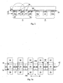
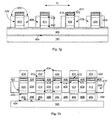
- Substantially parallel rails 20 include a plurality of line sets 21, each line set 21 consisting of two data lines 22 (22a and 22b, for example) and one reference line 24, reference line 24 immediately adjacent to and between the two data lines 22a and 22b.
- substantially parallel select lines 26 Above the rails 20 and preferably extending perpendicular to them are substantially parallel select lines 26.
- Select lines 26 are coextensive with gate dielectric layer 28 and channel layer 30. Transistors are formed between each adjacent data line and reference line pair. Transistor 34 includes channel region 41 between source region 40 and drain region 42. Each select line 26 controls the transistors it is associated with. Switchable resistor memory element 36 is disposed between channel region 41 and data line 22b. In this embodiment, adjacent transistors share a reference line; for example transistor 38 shares a reference line 24 with transistor 34. Transistor 38 also includes a switchable resistor memory element 36 between channel region 41 and data line 22a. No transistor exists between adjacent data lines 22b and 22c. As will be described, in preferred embodiments, a leakage path between data lines 22b and 22c is prevented either by doping channel layer 30 in this region or by removing this section of channel layer 30 using a channel trim masking step.
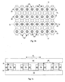
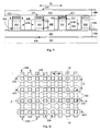
- Fig. 3a is a cross-sectional view of an example not part of the invention, in which the transistor is oriented substantially vertically.
- a plurality of substantially parallel data lines 50 is formed.
- Semiconductor pillars 52 are formed, each above one of the data lines 50.
- Each pillar 52 includes heavily doped regions 54 and 58 which serve as drain and source regions, and a lightly doped or undoped region 56 which serves as a channel region.
- region 56 could also be a stack of a plurality of thin doped semiconductor regions separated by a plurality of thin tunneling dielectric layers. Such a stack is preferred for very low leakage vertical TFT switches.
- a gate electrode 60 surrounds each pillar 52.
- Fig. 3b shows the cells of Fig. 3a viewed from above.
- pitch is the distance between a feature and the next occurrence of the same feature.
- the pitch of pillars 52 is the distance between the center of one pillar and the center of the adjacent pillar.
- pillars 52 In one direction pillars 52 have a first pitch P 1 , while in other direction, pillars 52 have a larger pitch P 2 ; for example P 2 may be 1.5 times larger than P 1 .
- Feature size is the width of the smallest feature or gap formed by photolithography in a device. Stated another way, pitch P 1 may be double the feature size, while pitch P 2 is three times the feature size.
- Fig. 3a shows the structure in cross-section along line X-X' of Fig. 3b
- Fig. 3c shows the structure in cross-section along line Y-Y' of Fig. 3b
- For readability reference lines 64 are omitted from Fig. 3b .
- reference lines 64 preferably parallel to data lines 50, are formed above the pillars 52, such that each pillar 52 is vertically disposed between one of the data lines 50 and one of the reference lines 54.
- a switchable resistor memory element 66 is formed in each memory cell between source region 58 and a reference line 64, for example.
- a switchable resistor memory element can be formed between drain region 54 and data line 50.
- Each memory cell of this embodiment has a vertically oriented transistor having a polycrystalline channel region and a switchable resistor memory element, the two electrically in series.
- the overall channel orientation is lateral, not vertical.
- Both of these embodiments is based on a nonvolatile memory cell comprising a switchable resistor memory element; and a thin film transistor having a channel region, wherein the switchable resistor memory element is disposed in series with the thin film transistor, wherein the switchable resistor memory element decreases resistance when a set voltage magnitude is applied across the resistive memory element, and wherein the switchable resistor memory element increases resistance when an reset voltage magnitude is applied across the switchable resistor memory element, and wherein the polarity of the set voltage magnitude is opposite the polarity of the reset voltage magnitude.
- the transistor and switchable resistor memory element are electrically disposed between a data line and a reference line, the reference line substantially parallel to the data line.
- the channel region of the transistor is electrically disposed between the data line and the reference line.
- the select line comprises the gate electrodes of the transistors it selects.
- the thin film transistor of the present invention it is preferred for the thin film transistor of the present invention to have low threshold voltage and high current.
- the channel region of each transistor may be formed of silicon, in preferred embodiments, channel region is germanium or a silicon-germanium alloy.
- This substrate 100 can be any semiconducting substrate as known in the art, such as monocrystalline silicon, IV-IV compounds like silicon-germanium or silicon-germanium-carbon, III-V compounds, II-VII compounds, epitaxial layers over such substrates, or any other semiconducting material.
- the substrate may include integrated circuits fabricated therein.
- the insulating layer 102 is formed over substrate 100.
- the insulating layer 102 can be silicon oxide, silicon nitride, high-dielectric film, Si-C-O-H film, or any other suitable insulating material.
- Conductive material 104 is deposited on insulating layer 102.
- Conductive material 104 is of any appropriate conductive material or stack of materials. At least the top portion of conductive material 104 is preferably heavily doped silicon.
- conductive material 104 is a layer of in situ doped silicon, preferably heavily doped with an n-type dopant such as phosphorus.
- Conductive material 104 can be any appropriate thickness, for example between about 100 and about 250 nm thick.
- a reservoir of mobile metal ions 106 is deposited. This layer is between about 1 and about 100 nm thick, preferably between about 10 and about 30 nm thick. Ion reservoir 106 is any material that can provide suitable mobile metal ions, preferably silver ions.
- Layer 108 is a solid electrolyte material, preferably comprising chalcogenide glass, of the formula A X B Y , where A includes at least one element from Group IIIA (B, Al, Ga, In, Ti), Group IVA (C, Si, Ge, Sn, Pb), Group VA (N, P, As, Sb, Bi), or Group VIIA (F, Cl, Br, I, At) of the periodic table, where B is selected from among S, Se and Te and mixtures thereof.
- the dopant is selected from among the noble metals and transition metals, including Ag, Au, Pt, Cu, Cd, Ir, Ru, Co, Cr, Mn or Ni.
- Chalcogenide layer 108 is preferably formed in an amorphous state. Layer 108 is in contact with ion reservoir 106.
- chalcogenide memories operate by undergoing phase change between an amorphous and a crystalline state.
- the memory cells of embodiments of the present invention have a different mechanism, formation and dissolution of a conductive bridge, and should not undergo phase change.
- chalcogenides that enter the crystalline phase less easily may be preferred.
- chalcogenide other materials that can support formation and dissolution of a conductive bridge may be substituted for a chalcogenide.
- layer 108 this description will refer to layer 108 as a chalcogenide layer, but it will be understood that other materials can be used instead.
- Chalcogenide layer 108 is preferably between about 10 and about 50 nm thick, preferably about 35 nm thick.
- Top electrode 110 is any appropriate electrode material. This should be a material that will not readily provide mobile metal ions to chalcogenide layer 108 under an electric field.
- Top electrode 110 can be, for example, tungsten, nickel, molybdenum, platinum, metal silicides, conductive nitrides such as titanium nitride, or heavily doped polysilicon.
- Top electrode 110 is preferably between about 10 and about 50 nm thick.
- top electrode 110 is not formed of heavily doped n-type polysilicon, a thin layer 112 of heavily doped n-type (N+) polysilicon is deposited next. This layer can be in situ doped or doped through ion implantation. Other appropriate barrier layers, adhesion layers, or etch stop layers may be included in addition to the layers described.
- conductive material 104, ion reservoir 106, chalcogenide layer 108, top electrode 110, and N+ layer 112 are patterned and etched into a plurality of substantially parallel, substantially coplanar lines 200.
- Dielectric fill 114 for example HDP oxide, is deposited over and between lines 200, filling gaps between them.
- the overfill of dielectric fill 114 is removed to expose N+ layer 112 at the tops of lines 200, and a planarizing step, for example by chemical-mechanical planarization (CMP) or etchback, coexposes N+ layers 112 and dielectric fill 114 at a substantially planar surface.
- CMP chemical-mechanical planarization
- etchback coexposes N+ layers 112 and dielectric fill 114 at a substantially planar surface.
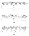
- the structure at this point is shown in Fig. 4a .
- a masking step is performed to expose every third line among lines 200, and N+ layer 112, top electrode 110, chalcogenide layer 108, and ion reservoir 106 are etched and removed from the exposed lines only.
- the exposed lines will be reference lines in the completed array.
- layers 112, 110, 108, and 106 remain on the other two of three lines, which will become data lines in the completed array.
- Ion reservoir 106, chalcogenide layer 108, and electrode layer 110 form a switchable resistor memory element.
- a channel layer 116 is deposited.
- This layer is a semiconductor material, preferably lightly doped with a p-type dopant, and is preferably between about 10 and about 50 nm thick. In preferred embodiments, channel layer 116 is between about 10 and about 20 nm thick.
- Channel layer 116 is a semiconductor material, and can be silicon, germanium, or an alloy of silicon, germanium, or silicon and germanium. In preferred embodiments, channel layer 116 is amorphous as deposited, and will be crystallized in a following anneal step or during subsequent thermal processing, and after recrystallization will be polycrystalline. Methods to maximize grain size in deposited semiconductor channel layers are described in Gu, US Patent No.
- n-type dopant atoms will diffuse up from N+ layers 112 and from N+ material 104 to form N+ regions in channel layer 116, which will behave as source and drain regions in the completed device.
- Channel layer 116 is conformal, following the topography over which it is deposited. At the top of reference lines R 1 and R 2 where layers 112, 110, 108, and 106 were removed, then, channel layer 116 has a corrugated shape. This corrugated shape increases effective channel length, which may improve device performance at very small dimensions.
- transistors will be formed between adjacent data lines and reference lines, but there should be no device formed between adjacent data lines, for example between data line D 2 and data line D 3 . Leakage between these lines can be prevented by a masking step and an ion implantation step, implanting a p-type dopant in the channel layer between data line D 2 and D 3 as shown in Fig. 4c .
- channel layer 116 can be selectively removed in region 117 between data lines D 2 and D 3 using conventional pattern and etch techniques.
- gate dielectric 120 is formed next.
- channel layer 116 is silicon or a silicon-rich alloy
- gate dielectric 120 may be a layer of silicon dioxide grown by an oxidation process such as thermal or plasma oxidation. In other embodiments, this layer is a deposited dielectric, for example silicon dioxide or higher-K dielectric materials such as Si 3 N 4 , Al 2 O 3 , HfO 2 , HfSiON, or Ta 2 O 5 .
- Gate dielectric layer 120 is preferably between about 2 and about 10 nm. Higher-K dielectric gate dielectrics may be thicker than a gate dielectric formed of silicon dioxide.
- Word line material 122 can be any conductive material, including tungsten, aluminum, or heavily doped semiconductor material, for example polysilicon.
- word line material 122 includes a first layer of n-type polysilicon, a thin layer of titanium, a thin layer of titanium nitride, and a second layer of n-type polysilicon. The titanium and titanium nitride will react with the surrounding polysilicon to form a titanium silicide layer, providing lower resistance.
- word lines 300 are formed. This etch continues through gate dielectric layer 120, channel layer 116, and through N+ layer 112 and top electrode 110. In preferred embodiments, etching continues through chalcogenide layer 108 as well. Word lines 300 must be fully isolated; chalcogenide layer 108 is typically high-resistance, but in a very large array even the low-conductance paths afforded by remaining chalcogenide material between adjacent word lines may be disadvantageous. Ion reservoir 106 is optionally etched as well. Fig. 4e shows the structure at ninety degrees along line L-L' to the view shown in Fig. 4d after the word line etch is completed.
- a dielectric material 124 is deposited over and between word lines 300, filling gaps between them.
- a planarizing step for example by CMP, forms a substantially planar surface on an interlevel dielectric formed of dielectric material 124.
- a first memory level has been formed. Additional memory levels can be formed above this level.
- chalcogenide layer 108 is replaced with amorphous silicon doped with V, Co, Ni, Pd, Fe or Mn, and is sandwiched between appropriate electrode layers.
- chalcogenide layer 108 is replaced with one of the perovskite materials named earlier. Any appropriate electrode materials may be used with a perovskite material, for example aluminum, titanium, vanadium, manganese, copper, niobium, zirconium, silver, tin, indium, hafnium, tantalum, or tungsten.
- a carbon polymer may replace chalcogenide layer 108 in another embodiment.
- the data line and the reference line are below the channel region and substantially parallel.
- a first voltage is applied to the data line and a second voltage is applied to the reference line, the first voltage higher than the second voltage.
- a third voltage is applied to the data line and a fourth voltage is applied to the reference line, the fourth voltage higher than the third voltage.
- fabrication begins over a suitable substrate 100 and insulating layer 102.
- substrate 100 may include integrated circuits fabricated therein.
- Data lines 400 are formed over the substrate 100 and insulator 102.
- An adhesion layer 404 may be included between the insulating layer 102 and the conducting layer 406 to help the conducting layer 406 adhere.
- a preferred material for the adhesion layer 404 is titanium nitride, though other materials may be used, or this layer may be omitted.
- Adhesion layer 404 can be deposited by any conventional method, for example by sputtering.
- the thickness of adhesion layer 404 can range from about 20 to about 500 angstroms (2 to 50 nm), and is preferably between about 10 and about 40 nm, most preferably about 20 nm.
- Conducting layer 406 can comprise any conducting material known in the art, such as doped semiconductor material, metals such as tungsten, or conductive metal silicides, or aluminum.
- the thickness of conducting layer 406 can depend, in part, on the desired sheet resistance and therefore can be any thickness that provides the desired sheet resistance. In one embodiment, the thickness of conducting layer 406 can range from about 50 to about 300 nm, preferably between about 100 and about 200 nm, most preferably about 120 nm.
- Another layer 410 preferably of titanium nitride, is deposited on conducting layer 406. It may have thickness comparable to that of layer 404.
- the layers will be patterned and etched using any suitable masking and etching process to form substantially parallel, substantially coplanar data lines 400, shown in Fig. 5a in cross-section.
- Dielectric material 408 is deposited over and between data lines 400.
- Dielectric material 408 can be any known electrically insulating material, such as HDP oxide.
- the width of data lines 400 can be as desired.
- data lines 200 can have a width between about 20 and about 250 nm, preferably between about 45 and about 90 nm.
- the gaps between data lines 400 have about the same width as data lines 400, though it may be greater or less.
- the pitch of data lines 200 is between about 40 nm and about 500 nm, preferably between about 90 nm and about 180 nm.
- Fig. 5b vertical pillars will be formed above completed data lines 400.
- Semiconductor material that will be patterned into pillars is deposited.
- the semiconductor material can be silicon, germanium, or an alloy of silicon, germanium, or silicon and germanium.
- the semiconductor pillar comprises a bottom heavily doped region of a first conductivity type, a middle lightly doped or undoped region of a second conductivity type, and a top heavily doped region of the first conductivity type.
- bottom heavily doped region 412 is heavily doped n-type germanium.
- heavily doped region 412 is deposited and doped with an n-type dopant such as phosphorus by any conventional method, preferably by in situ doping, though alternatively through some other method, such as ion implantation.
- This layer is preferably between about 10 and about 80 nm, most preferably between about 20 and about 30 nm. Bottom heavily doped region 412 will behave as a source or drain region for the transistor to be formed.
- the lightly doped region 414 will preferably be between about 60 and about 200 nm thick, preferably between about 90 and about 150 nm thick.
- the top heavily doped region 416 should be between about 10 and about 50 nm thick, preferably between about 20 and about 30 nm thick. Thus between about 70 and about 200 nm of germanium should be deposited to complete the thickness required for the pillar.
- This germanium layer 414 is preferably lightly doped p-type germanium, and is preferably in-situ doped.
- the channel region of the transistor to be formed will be in germanium layer 414.
- a subsequent planarization step will remove some germanium, so in this case an extra thickness is deposited. If the planarization step is performed using a conventional CMP method, about 800 angstroms (80 nm) of thickness may be lost (this is an average; the amount varies across the wafer. Depending on the slurry and methods used during CMP, the germanium loss may be more or less.) If the planarization step is performed by an etchback method, only about 40 nm of germanium or less may be removed.
- top heavily doped n-type region 416 is formed at this point by ion implantation.
- Heavily doped region 416 which will serve as a source/drain region for the transistor to be formed, is preferably between about 20 and about 30 nm thick.
- a layer 421 of a reservoir of mobile metal ions is deposited.
- This layer is between about 1 and about 100 nm thick, preferably between about 10 and about 30 nm thick.
- Ion reservoir 421 is any material that can provide suitable mobile metal ions, preferably silver ions.
- a layer 418 of an ion conductor preferably a chalcogenide (corresponding to chalcogenide layer 108 in the previous embodiment) is deposited on and in contact with ion reservoir 421.
- the thickness and composition of layer 418 may be as described in the previous embodiment. For simplicity, this discussion will refer to ion conductor layer 418 as a chalcogenide layer, but it will be understood that other materials can be used instead.
- Next electrode layer 423 is deposited on chalcogenide layer 418.
- Layer 423 is any of the materials described for use in the top electrode layer of the previous embodiment.
- a pattern and etch step is performed to etch pillars 500.
- Layers 423, 418, 421, 416, 414, and 412 are etched in this etch step.
- the pillars 500 can be formed using any suitable masking and etching process.
- photoresist can be deposited, patterned using standard photolithography techniques, and etched, then the photoresist removed.
- a hard mask of some other material for example silicon dioxide, can be formed on top of the semiconductor layer stack, with bottom antireflective coating (BARC) on top, then patterned and etched.
- BARC bottom antireflective coating
- DARC dielectric antireflective coating
- pillars 500 include bottom heavily doped region n-type region 412, middle lightly doped p-type region 414, top heavily doped n-type region 416, ion reservoir 421, chalcogenide layer 418, and top electrode 423. In some embodiments other layers, for example barrier layers, may be included.
- the pillars 500 are preferably about the same width as data lines 400.
- Fig. 5c which shows the structure viewed from above, it will be seen that pillars 500 have a first pitch P 3 in one direction and a second, larger pitch P 4 in the other direction.
- Pillars 500 are pictured, in Fig. 5c , as substantially cylindrical. At small feature sizes, the photolithographic process tends to round comers; thus independently patterned pillars will tend to be cylindrical.
- the views of Figs. 5a and 5b show pillars at the smaller pitch P 3 , along line Z-Z' of Fig. 5c .
- Pitch P 3 measured in the direction perpendicular to data lines 400, should be about the same as the pitch of data lines 400 (preferably between about 180 and 360 nm), so that each pillar 500 is on top of one of the data lines 400. Some misalignment can be tolerated.
- Pitch P 4 measured parallel to data lines 400, should be larger than pitch P 3 , preferably about 1.5 times P 3 , though if desired it may be larger or smaller.
- Gate dielectric layer 426 is conformally deposited over pillars 500, surrounding and in contact with each pillar 500.
- Gate dielectric layer 426 can be any appropriate material, for example silicon dioxide, and may have any appropriate thickness, for example between about and about 80 angstroms (2-8 nm), preferably about 50 angstroms (5 nm).
- Gate material layer 428 is deposited over gate dielectric layer 426, over and between first pillars 500.
- Gate material layer 428 is preferably tantalum nitride, though any other suitable conductive material, for example heavily doped silicon or a metal, can be used instead.
- Fig. 5e shows the structure of Fig. 5d viewed at 90 degrees, along line W-W' of Fig. 5c .
- the thickness of tantalum nitride layer 428 is selected so that the sidewalls merge in one direction (having smaller pitch P 3 ) but not in the other direction (having larger pitch P 4 ).
- pitch P 3 is 180 nm
- pitch P 4 is 270 nm.
- the width of pillars 500 is about 90 nm, and the gap between them, in the direction of smaller pitch P 3 , is about 90 nm; thus the gap between pillars 300 in the P 4 pitch direction is 180 nm.
- a thickness of about 45 nm of tantalum nitride layer 428 will just fill gaps in the P 3 pitch direction (shown in Fig. 5d ), and will leave a gap G of 90 nm in the P 4 pitch direction (shown in Fig. 5e .)
- the thickness of tantalum nitride layer 428 is between one-half the width of pillars 500 and about three-quarters the width of pillars 500.
- the preferred thickness of tantalum nitride layer 428 is between about 45 nm and about 72 nm, preferably about 60 nm.
- a thickness of 60 nm will leave a gap of about 60 nm in the P 4 pitch direction.
- etching is performed to recess tantalum nitride layer 428 and to isolate select lines 430.
- Select lines 430 consist of merged tantalum nitride layer 428 in the P 3 pitch direction ( Fig. 5f ), but should be fully separate in the P 4 pitch direction ( Fig. 5g ).
- Select lines 430 are substantially parallel and substantially coplanar.
- tantalum nitride layer 428 is preferably at least 50 nm below the top of top electrode 423. This 50 nm gap will be filled with dielectric, and will serve to isolate select lines 430 from overlying conductors yet to be formed. Tantalum nitride layer 428 should not be etched so far, however, that it fails to reach the lower edge of heavily doped region 416, which will be the source/drain region of the transistor.
- dielectric material 408 is deposited over and between pillars 500 and tantalum nitride layer 428, filling the gaps between them.
- Dielectric material 408 can be any known electrically insulating material, for example HDP oxide.
- dielectric material on top of the pillars 500 is removed, exposing top electrodes 423 separated by dielectric material 138.
- Gate dielectric layer 426 is removed from above top electrode 423 at the same time. This removal of dielectric overfill and planarization can be performed by any process known in the art, such as CMP or etchback.
- Substantially parallel, substantially coplanar reference line 600 can be formed by any suitable method.
- Reference lines 600 can be formed using the methods used to form data lines 400: Deposit titanium nitride layer 432, deposit conductive layer 434, deposit titanium nitride layer 436, then pattern and etch to form reference lines 600.
- Reference lines 600 are preferably parallel to data lines 400, though, in an alternative embodiment, reference lines 600 could be formed perpendicular to data lines 400 if preferred.
- a dielectric material (not shown) is deposited over and between reference lines 600.
- reference lines 600 can be formed by a damascene method.
- Reference lines 600 preferably have about the same width as data lines 400.
- the pitch of reference lines should be pitch P 3 , so that each pillar 500 is vertically disposed between one of the data lines 400 and one of the reference lines 600. Some misalignment can be tolerated.
- reference lines 600 can be formed by a damascene method, for example comprising copper. If reference lines 600 are formed by a damascene method, they will be formed by depositing a dielectric material; etching substantially parallel trenches in the dielectric material; depositing a conductive material on the dielectric material, filling the trenches; and planarizing to expose the dielectric material and form the reference lines 600.
- Fig. 5j shows the structure viewed from above.
- the view of Fig. 5h is along line Z-Z'
- the view of Fig. 5i is along line W-W'.
- one of the data line and the reference line is below the channel region and the other is above the channel region.
- Figs. 5h and 5i What has been formed in Figs. 5h and 5i is a first memory level.
- tantalum nitride layer 428 serves as a gate electrode.
- threshold voltage is applied to gate electrode 428, a vertical conductive channel is formed at the surface of channel region 414, and current may flow between source/drain regions 412 and 416.
- Each gate electrode is a portion of one of the select lines 430.
- Ion reservoir 421, chalcogenide layer 418, and top electrode 423 serve as a switchable resistor memory element. Additional memory levels can be formed above this memory level, using the methods described.
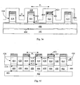
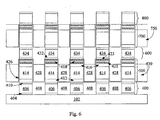
- FIG. 6 shows two memory levels sharing reference lines 600.
- FIG. 7a shows four memory levels: Memory levels M 1 and M 2 share reference lines 610, memory levels M 2 and M 3 share data lines 710, and memory levels M 3 and M 4 share reference lines 810.
- Fig. 7b shows four memory levels in which reference lines (610 and 810) are shared, but data lines (710 and 712) are not shared between the memory levels M 2 and M 3 .
- the arrangement of Fig. 7a requires fewer masking steps, and may be preferable for that reason.
- control circuitry is formed in the substrate beneath the memory, and electrical connections must be made from the ends of the data lines, reference lines, and select lines of the array to this circuitry.
- Advantageous schemes for making these connections while minimizing use of substrate area are described in Scheuerlein et al., US Patent No. 6,879,505 , "Word line arrangement having multi-layer word line segments for three-dimensional memory array; and in Scheuerlein et al., US Patent Application No. 10/403,752 , “Three-Dimensional Memory Device Incorporating Segmented Bit Line Memory Array,” filed March 31, 2003 (published as US 7,233,024 ), both owned by the assignee of the present invention and hereby incorporated by reference.
- the arrangement of Fig. 7b while requiring more masking steps, can make use of the techniques described by Scheuerlein et al., and my be preferred for that reason.
- Both of the embodiments described include a nonvolatile memory cell comprising a switchable resistor memory element; and a transistor comprising a channel region, the switchable resistor memory element and the transistor arranged in series, wherein the transistor is electrically connected between a data line and a reference line, both data line and reference line extending in a first direction, wherein, when the transistor is on, current flows through the channel region in a second direction, the second direction substantially perpendicular to the first direction, wherein the switchable resistor memory element decreases resistance when subjected to a set voltage magnitude and increases resistance when subjected to a reset voltage magnitude, and wherein polarity of the set voltage magnitude and the reset voltage magnitude are opposite.
- data lines and reference lines are parallel and are preferably perpendicular to select lines. This is advantageous because many cells can be selected by a select line. All of these cells have some current activity, and if a reference line were parallel to such a select line, all those currents would pass through the reference line, and the I-R drop would be multiplied many times.
- the data line and reference line are perpendicular to the direction of current flow through the channel of the transistor.
- DRAM devices having a similar configuration are described in Scheuerlein, US Patent Application No. 11/157,293 , “Floating Body Memory Cell System and Method of Manufacture,” (published as US 2006/285422 ) and in Scheuerlein US Patent Application No. 11/157,317 , “Volatile Memory Cell Two-Pass Writing Method,” (published as US 7,317,641 ), both filed June 20, 2005.
- Resistance across the thin film transistor of the present invention is important to device performance. For reasons described more fully in the related applications filed on even date herewith, it is preferable for the resistance of the thin film transistor to comparable to the low-resistance state of the switchable resistor memory element.
- resistance of the channel region is decreased by use of germanium or silicon-germanium alloys.
- use of very thin gate dielectrics and of high-K dielectric gate materials helps keep resistance of the transistor low.
- the set voltage magnitude and the reset voltage magnitude used in preferred embodiments of the present invention in general are less than about 2 volts, preferably less than about 1 volt.
- a monolithic three dimensional memory array is one in which multiple memory levels are formed above a single substrate, such as a wafer, with no intervening substrates.
- the layers forming one memory level are deposited or grown directly over the layers of an existing level or levels.
- stacked memories have been constructed by forming memory levels on separate substrates and adhering the memory levels atop each other, as in Leedy, US Patent No. 5,915,167 , "Three dimensional structure memory.”
- the substrates may be thinned or removed from the memory levels before bonding, but as the memory levels are initially formed over separate substrates, such memories are not true monolithic three dimensional memory arrays.
- a monolithic three dimensional memory array formed above a substrate comprises at least a first memory level formed at a first height above the substrate and a second memory level formed at a second height different from the first height. Three, four, eight, or indeed any number of memory levels can be formed above the substrate in such a multilevel array.
- Examples include a monolithic three dimensional memory array comprising: a) a first memory level formed above a substrate, the first memory level comprising a first plurality of memory cells, each first memory cell comprising: i) a field effect transistor; and ii) a switchable resistor memory element, wherein the switchable resistor memory element decreases resistance when subjected to a set voltage magnitude and increases resistance when subjected to a reset voltage magnitude, and wherein polarity of the set voltage magnitude and the reset voltage magnitude are opposite; and b) a second memory level monolithically formed above the first memory level.
- the second memory level comprises a second plurality of memory cells.
- first, second, and additional pluralities of switchable resistor memory elements may be formed at different heights above a substrate.
- Embodiments of the present invention provide for a method for forming, setting and resetting a nonvolatile memory cell and associated conductors, the method comprising: forming a first data line extending in a first direction; forming a first reference line extending in the first direction; forming a thin film transistor having a channel region, the channel region disposed electrically between the first data line and the first reference line; forming a switchable resistor memory element disposed between the channel region and the data line, the resistive switching memory element having a first resistance; forming a first select line extending in a second direction different from the first direction; applying a set voltage magnitude across the switchable resistor memory element wherein, after application of the set voltage magnitude, the switchable resistor memory element has a second resistance lower than the first resistance; and applying a reset voltage magnitude across the switchable resistor memory element wherein, after application of the reset voltage magnitude, the switchable resistor memory element has a third resistance higher than the second resistance, and wherein the polarity of the set voltage magnitude and
Landscapes
- Engineering & Computer Science (AREA)
- Manufacturing & Machinery (AREA)
- Chemical & Material Sciences (AREA)
- Materials Engineering (AREA)
- Semiconductor Memories (AREA)
- Semiconductor Integrated Circuits (AREA)
- Read Only Memory (AREA)
- Non-Volatile Memory (AREA)
Abstract
Description
- The invention relates to a nonvolatile memory cell.
- There are materials that have at least two distinct stable resistivity states. This class of materials can be switched from a high-resistivity state to a low-resistivity state by applying a voltage magnitude across the material in a first direction. To switch the material from the low-resistivity state back to a high-resistivity state, the voltage magnitude can be reversed.
- Some of these materials can be switched between resistivity states at relatively low applied voltages, for example two volts or less, and preferably one volt or less. These properties would make these materials attractive for use in nonvolatile memory arrays, which retain their memory state even when power is removed from the device. Low-voltage switching is advantageous to reduce power consumption in devices, but many challenges must be overcome to provide the low voltages and reversible voltages required to operate cells incorporating such material, and to avoid accidental change of state during read or during the writing of other cells in a large array of cells.
[0004A] ZHUANG W W ET AL : "Novel colossal magnetoresistive thin film non-volatile resistance random access memory (RRAM)" International Electron Devices Meeting 2002. IEDM. Technical Digest. San Francisco, CA, Dec. 8-11, 2002, New York, NY : IEEE, US, 8 December 2002 (2002-12-08), pages 193-196 discloses a non-volatile memory cell according to the preamble of Claim 1.
[0004B]EP 1 441 361 discloses a method according to the preamble of Claim 9.
[0004C]US 2004/0041761 discloses a memory element provided in series with a thin film transistor. The memory element has a varying resistance depending on the magnitude of the voltage applied to it. - The present invention is defined by the following claims, and nothing in this section should be taken as a limitation on those claims. In general, the invention is directed to a non-volatile memory cells adapted for use in a rewriteable memory array.
- According to an aspect of the present invention there is provided a non-volatile memory cell comprising: a switchable resistor memory element and a transistor comprising a channel region. The switchable resistor memory element and the transistor are arranged in series, wherein the transistor is electrically connected between a data line and a reference line. Both of the data line and the reference line extending in a first direction, wherein, when the transistor is on, current flows through the channel region in a second direction. The second direction substantially perpendicular to the first direction. The switchable resistor memory element decreases resistance when subjected to a set voltage magnitude and increases resistance when subjected to a reset voltage magnitude. The polarities of the set voltage magnitude and the reset voltage magnitude are opposite. The data line and the reference line are below the channel region.
- According to another aspect of the present invention there is provided a method for forming, setting and resetting a non-volatile memory cell and associated conductors. The method comprises forming a first data line extending in a first direction forming a first reference line extending in the first direction, forming a transistor having a channel region, the channel region disposed electrically between the first data line and the first reference line; forming a switchable resistor memory element disposed between the channel region and the data line, the switchable resistor memory element having a first resistance, forming a first select line extending in a second direction different from the first direction, applying a set voltage magnitude across the switchable resistor memory element wherein, after application of the set voltage magnitude, the resistive switching memory element has a second resistance lower than the first resistance, and applying a reset voltage magnitude across the switchable resistor memory element wherein, after application of the reset voltage magnitude, the switchable resistor memory element has a third resistance higher than the second resistance, and wherein the polarity of the set voltage magnitude and the reset voltage magnitude are opposite. The transistor is a thin film transistor. The data line and the reference line are below the channel region.
- The nonvolatile memory cell may be formed above a substrate, the memory cell comprising a thin film transistor comprising a channel region, the channel region comprising a deposited semiconductor material, wherein the semiconductor material is silicon, germanium or a silicon-germanium alloy.
- Further disclosed but not part of the invention is a monolithic three dimensional memory array comprising a) a first memory level formed above a substrate, the first memory level comprising a first plurality of memory cells, each first memory cell comprising: i) a field effect transistor; and ii) a switchable resistor memory element, wherein the switchable resistor memory element decreases resistance when subjected to a set voltage magnitude and increases resistance when subjected to a reset voltage magnitude, and wherein polarity of the set voltage magnitude and the reset voltage magnitude are opposite; and b) a second memory level monolithically formed above the first memory level.
- Further disclosed but not part of the invention is a monolithic three dimensional memory array comprising a first plurality of substantially parallel, substantially coplanar lines extending in a first direction; a second plurality of substantially parallel, substantially coplanar lines extending in a second direction; a first plurality of switchable resistor memory elements, each switchable resistor memory element disposed electrically between one of the first lines and one of the second lines, the first switchable resistor memory elements at a first height above a substrate; and a second plurality of switchable resistor memory elements, the second switchable resistor memory elements at a second height above the first height, wherein the switchable resistor memory elements decrease resistance when subjected to a set voltage magnitude and increase resistance when subjected to a reset voltage magnitude, and wherein polarity of the set voltage magnitude and the reset voltage magnitude are opposite.
- A method for forming, setting and resetting a nonvolatile memory cell and associated conductors is also disclosed. The method comprises forming a first data line extending in a first direction; forming a first reference line extending in the first direction; forming a thin film transistor having a channel region, the channel region disposed electrically between the first data line and the first reference line; forming a switchable resistor memory element disposed between the channel region and the data line, the switchable resistor memory element having a first resistance; forming a first select line extending in a second direction different from the first direction; applying a set voltage magnitude across the switchable resistor memory element wherein, after application of the set voltage magnitude, the resistive switching memory element has a second resistance lower than the first resistance; and applying a reset voltage magnitude across the switchable resistor memory element wherein, after application of the reset voltage magnitude, the switchable resistor memory element has a third resistance higher than the second resistance, and wherein the polarity of the set voltage magnitude and the reset voltage magnitude are opposite.
- Each of the aspects and embodiments of the invention described herein can be used alone or in combination with one another.
- The preferred aspects and embodiments will now be described with reference to the attached drawings.
-
Fig. 1a-1d are cross-sectional views illustrating formation and dissolution of a conductive bridge in a switchable resistor memory element for use in a memory cell formed according to a preferred embodiment of the present invention. -
Fig. 2 is a cross-sectional view of a memory level formed according to a preferred embodiment of the present invention. -
Figs. 3a ,3b, and 3c are views of a memory level formed according to an example.Figs. 3a and3c are cross-sectional views, whileFig. 3b is a plan view. -
Figs. 4a-4f are cross-sectional views illustrating stages in formation of a memory level according to a preferred embodiment of the present invention. -
Figs. 5a-5j are views illustrating stages in formation of a memory level according to an example.Figs. 5c and5j are plan views, while the remainder are cross-sectional views. -
Fig. 6 is a cross-sectional view illustrating two memory levels sharing reference lines according to an example. -
Fig. 7a is a cross-sectional view illustrating two memory levels sharing data lines according to an example, whileFig. 7b is a cross-sectional view illustrating two memory levels not sharing data lines according to a different example. - It has been noted that some materials can be reversibly switched between more than one stable resistivity state, for example between a high-resistivity state and a low-resistivity state. The conversion from a high-resistivity state to a low-resistivity state will be called the set conversion, while the conversion from a low-resistivity state to a high-resistivity state will be called the reset conversion. Petti,
US Patent Application No. 11/143,269 US 2006/0273298 ), describes a monolithic three dimensional memory array comprising transistors and resistance-switching memory elements, wherein setting and resetting can be performed with the same voltage polarity on the resistance-switching memory element. The resistance-switching memory elements of Petti require relatively large voltages (2-3 volts, for example) and currents for either the set or the reset conversion. - For certain materials, in contrast to those preferred in Petti, the conversion from a high-resistivity state to low-resistivity state is affected by applying a voltage of a certain magnitude, called a set voltage magnitude, in one direction, while the reverse conversion, from a low-resistivity state to a high resistivity state, is affected by applying a voltage magnitude, called a reset voltage magnitude, in the opposite direction. These materials thus are bi-directional. One such material is amorphous silicon doped with V, Co, Ni, Pd, Fe or Mn (these materials are described more fully in Rose et al.,
US Patent No. 5,541,869 .) Another class of material is taught byIgnatiev et al. in US Patent No. 6,473,332 : these are perovskite materials such as Pr1-XCaXMnO3, La1-XCaXMnO3 (LCMO), LaSrMnO3 (LSMO), or GdBaCoXOY (GBCO). Another option for this variable-resistance material is a carbon-polymer film comprising carbon black particulates or graphite, for example, mixed into a plastic polymer, as taught byJacobson et al. in US Patent No. 6,072,716 . - A preferred material is taught by
Campbell et al. in US Patent Application No. 09/943190 granted as US 6,881,623 ), and byCampbell in US Patent Application No. 09/941544 published as US 2003/047 765 ). This materials is doped chalcogenide glass of the formula AXBY, where A includes at least one element from Group IIIA (B, Al, Ga, In, Ti), Group IVA (C, Si, Ge, Sn, Pb), Group VA (N, P, As, Sb, Bi), or Group VIIA (F, Cl, Br, I, At) of the periodic table, where B is selected from among S, Se and Te and mixtures thereof The dopant is selected from among the noble metals and transition metals, including Ag, Au, Pt, Cu, Cd, Ir, Ru, Co, Cr, Mn or Ni. As will be described, in an embodiment of the present invention this chalcogenide glass (amorphous chalcogenide, not in as crystalline state) is formed in a memory cell adjacent to a reservoir of mobile metal ions. Some other solid electrolyte material could substitute for chalcogenide glass. -
Fig. 1a shows a switchableresistor memory element 8 includingchalcogenide layer 10 located between two electrodes.Chalcogenide layer 10 is amorphous, and is high-resistivity as formed, so switchableresistor memory element 8 is in a high-resistance state.Electrode 12 is a source of mobile metal ions, preferably silver.Electrode 14 is any conductor which will not readily provide mobile metal ions, for example tungsten, aluminum, nickel, platinum, or heavily doped semiconductor material. - Turning to
Fig. 1b , when a positive voltage is applied tosilver electrode 12 and a negative voltage toelectrode 14, electrons flow towardelectrode 12, while silver ions (shown as small circles) migrate fromelectrode 12 intochalcogenide layer 10. As shown inFig. 1c , the silver forms a conductive bridge acrosschalcogenide layer 10, and switchableresistor memory element 8 is in a low-resistance state. The memory cell including switchableresistor memory element 8 has been set, or converted to a low-resistance state. The difference in resistance between the low-resistance and high-resistance states of switchableresistor memory element 8 is readily and repeatably detectable, and in this way a memory state (data "0" or data "1", for example) can be stored and read. - Referring to
Fig. 1d , to reset the memory cell, the voltage is reversed. A negative voltage is applied toelectrode 12 and a positive voltage toelectrode 14. Electrons flow towardelectrode 14, the silver inchalcogenide layer 12 is oxidized, and silver ions migrate back intoelectrode 12, breaking the conductive bridge, leavingchalcogenide layer 12 once again high-resistance. This set and reset cycle can be repeated many times. - It is important to carefully control the circuit conditions experienced by each cell during read, set, and reset. If, during set, too little current is used to form the conductive bridge, the cell will not be highly conductive, and the difference between the programmed and unprogrammed state will be difficult to detect. If too much current is applied, the conductive bridge formed across the chalcogenide layer becomes so conductive that when a reset is attempted, the resistance of the conductive bridge is too low (the current is too high) to allow enough voltage to build up to cause the silver in the bridge to oxidize and to migrate back to
electrode 12. - During a read operation, voltage must be applied across the cell to detect current flow and hence the resistance of the switchable resistor memory element, and from the resistance to determine the corresponding data state of the memory cell. If too much voltage is applied, however, there is danger that an undesired high-to-low-resistance or low-to-high-resistance conversion will inadvertently be triggered.
- When many cells including such switchable resistor memory elements are included in a large memory array, control of the voltages experienced by each cell becomes more difficult. The present invention describes a nonvolatile memory cell that stores a data state in the state of a switchable resistor memory element, wherein the switchable resistor memory element decreases resistance when subjected to a set voltage magnitude and increases resistance when subjected to a reset voltage magnitude, and wherein polarity of the set voltage and the reset voltage are opposite. The memory cell of preferred embodiments of the present invention is adapted to be formed in large arrays, allowing for precise control of voltage conditions on each cell.
- A memory cell in a large array may be disturbed when voltage is applied to neighboring cells, for example to a cell on a shared conductor. In arrays such as that taught in, for example,
Herner et al., US Patent Application No. 11/125,939 US 2006/0250836 ) a resistance-switching material is paired with a diode to provide electrical isolation. A diode is not the most advantageous choice to use with materials such as those described herein. The resistance-switching materials of the present invention require bi-directional voltage or current, while a diode is a one-way device. In addition, the relatively low switching voltages of some of the resistance-switching materials used in the present invention are difficult to achieve given the relatively high turn-on voltages associated with conventional diodes. - In preferred embodiments of the present invention, a bi-directional switchable resistor memory element is paired with a MOSFET. In preferred embodiments, the MOSFET is a thin-film transistor adapted to be formed in a monolithic three dimensional memory array, forming a highly dense memory device. As described in more in more detail in related
US patent application no. 11/179,123 US 7,345,907 )US patent application no. 11/179,077 US 7,362,604 ) the bias polarities for the read, set, and reset operations are chosen to avoid accidental disturb of the stored memory states during normal operation of the memory and thereby allow the use bi-directional switching resistor elements that switch resistance state at very low voltage in a TFT memory array. In an exemplary embodiment, the set bias is positive and the reset and read bias negative. - Two families of embodiments will be described. Turning to
Fig. 2 , a first embodiment includes memory cells in a TFT array, each having a transistor and a switchable resistor memory element in series. It will be understood that many other embodiments may fall within the scope of the invention. These embodiments are provided for clarity and are not intended to be limiting. Substantially parallel rails 20 (shown in cross section, extending out of the page) include a plurality of line sets 21, each line set 21 consisting of two data lines 22 (22a and 22b, for example) and onereference line 24,reference line 24 immediately adjacent to and between the twodata lines 22a and 22b. Above therails 20 and preferably extending perpendicular to them are substantially parallelselect lines 26.Select lines 26 are coextensive withgate dielectric layer 28 andchannel layer 30. Transistors are formed between each adjacent data line and reference line pair.Transistor 34 includes channel region 41 betweensource region 40 and drainregion 42. Eachselect line 26 controls the transistors it is associated with. Switchableresistor memory element 36 is disposed between channel region 41 and data line 22b. In this embodiment, adjacent transistors share a reference line; forexample transistor 38 shares areference line 24 withtransistor 34.Transistor 38 also includes a switchableresistor memory element 36 between channel region 41 anddata line 22a. No transistor exists betweenadjacent data lines 22b and 22c. As will be described, in preferred embodiments, a leakage path betweendata lines 22b and 22c is prevented either bydoping channel layer 30 in this region or by removing this section ofchannel layer 30 using a channel trim masking step. -
Fig. 3a is a cross-sectional view of an example not part of the invention, in which the transistor is oriented substantially vertically. A plurality of substantiallyparallel data lines 50 is formed.Semiconductor pillars 52 are formed, each above one of the data lines 50. Eachpillar 52 includes heavily dopedregions undoped region 56 which serves as a channel region. In an alternative embodiment,region 56 could also be a stack of a plurality of thin doped semiconductor regions separated by a plurality of thin tunneling dielectric layers. Such a stack is preferred for very low leakage vertical TFT switches. Agate electrode 60 surrounds eachpillar 52. -
Fig. 3b shows the cells ofFig. 3a viewed from above. In a repeating pattern, pitch is the distance between a feature and the next occurrence of the same feature. For example, the pitch ofpillars 52 is the distance between the center of one pillar and the center of the adjacent pillar. In onedirection pillars 52 have a first pitch P1, while in other direction,pillars 52 have a larger pitch P2; for example P2 may be 1.5 times larger than P1. (Feature size is the width of the smallest feature or gap formed by photolithography in a device. Stated another way, pitch P1 may be double the feature size, while pitch P2 is three times the feature size.) In the direction having the smaller pitch P1, shown inFig. 3a , thegate electrodes 60 of adjacent memory cells merge, forming a singleselect line 62. In the direction having larger pitch P2,gate electrodes 60 of adjacent cells do not merge, and adjacentselect lines 62 are isolated.Fig. 3a shows the structure in cross-section along line X-X' ofFig. 3b , whileFig. 3c shows the structure in cross-section along line Y-Y' ofFig. 3b . Forreadability reference lines 64 are omitted fromFig. 3b . - Referring to
Fig. 3a and3c ,reference lines 64, preferably parallel todata lines 50, are formed above thepillars 52, such that eachpillar 52 is vertically disposed between one of the data lines 50 and one of the reference lines 54. A switchableresistor memory element 66 is formed in each memory cell betweensource region 58 and areference line 64, for example. Alternatively, a switchable resistor memory element can be formed betweendrain region 54 anddata line 50. - Each memory cell of this embodiment has a vertically oriented transistor having a polycrystalline channel region and a switchable resistor memory element, the two electrically in series. In the embodiment of
Fig. 2 , in contrast, the overall channel orientation is lateral, not vertical. - Both of these embodiments is based on a nonvolatile memory cell comprising a switchable resistor memory element; and a thin film transistor having a channel region, wherein the switchable resistor memory element is disposed in series with the thin film transistor, wherein the switchable resistor memory element decreases resistance when a set voltage magnitude is applied across the resistive memory element, and wherein the switchable resistor memory element increases resistance when an reset voltage magnitude is applied across the switchable resistor memory element, and wherein the polarity of the set voltage magnitude is opposite the polarity of the reset voltage magnitude. The transistor and switchable resistor memory element are electrically disposed between a data line and a reference line, the reference line substantially parallel to the data line. Specifically, the channel region of the transistor is electrically disposed between the data line and the reference line. In both embodiments, the select line comprises the gate electrodes of the transistors it selects.
- For reasons to be described herein, and in the related applications, it is preferred for the thin film transistor of the present invention to have low threshold voltage and high current. Thus, while the channel region of each transistor may be formed of silicon, in preferred embodiments, channel region is germanium or a silicon-germanium alloy.
-
Lee et al., US Patent No. 6,881,994 , "Monolithic Three Dimensional Array of Charge Storage Devices Containing a Planarized Surface"; andWalker et al., US Patent Application No. 10/335,089 US 7,005,350 ) owned by the assignee of the present invention, describe monolithic three dimensional memory arrays in which the memory cells comprise transistors. - Detailed examples will be provided, one describing fabrication of a monolithic three dimensional memory array formed according to the embodiment of
Fig. 2 , and another describing fabrication of a monolithic three dimensional memory array formed according to the embodiment ofFigs. 3a-3c . Fabrication techniques described in Lee et al., in Walker et al., and in Petti will prove useful during fabrication of memory arrays. - Turning to
Fig. 4a , formation of the memory begins with asubstrate 100. Thissubstrate 100 can be any semiconducting substrate as known in the art, such as monocrystalline silicon, IV-IV compounds like silicon-germanium or silicon-germanium-carbon, III-V compounds, II-VII compounds, epitaxial layers over such substrates, or any other semiconducting material. The substrate may include integrated circuits fabricated therein. - An insulating
layer 102 is formed oversubstrate 100. The insulatinglayer 102 can be silicon oxide, silicon nitride, high-dielectric film, Si-C-O-H film, or any other suitable insulating material. -
Conductive material 104 is deposited on insulatinglayer 102.Conductive material 104 is of any appropriate conductive material or stack of materials. At least the top portion ofconductive material 104 is preferably heavily doped silicon. In preferred embodiments,conductive material 104 is a layer of in situ doped silicon, preferably heavily doped with an n-type dopant such as phosphorus.Conductive material 104 can be any appropriate thickness, for example between about 100 and about 250 nm thick. - Next a reservoir of
mobile metal ions 106 is deposited. This layer is between about 1 and about 100 nm thick, preferably between about 10 and about 30 nm thick.Ion reservoir 106 is any material that can provide suitable mobile metal ions, preferably silver ions. - An
ion conductor layer 108 is deposited next.Layer 108 is a solid electrolyte material, preferably comprising chalcogenide glass, of the formula AXBY, where A includes at least one element from Group IIIA (B, Al, Ga, In, Ti), Group IVA (C, Si, Ge, Sn, Pb), Group VA (N, P, As, Sb, Bi), or Group VIIA (F, Cl, Br, I, At) of the periodic table, where B is selected from among S, Se and Te and mixtures thereof. The dopant is selected from among the noble metals and transition metals, including Ag, Au, Pt, Cu, Cd, Ir, Ru, Co, Cr, Mn or Ni.Chalcogenide layer 108 is preferably formed in an amorphous state.Layer 108 is in contact withion reservoir 106. - Note that some chalcogenide memories operate by undergoing phase change between an amorphous and a crystalline state. As described, the memory cells of embodiments of the present invention have a different mechanism, formation and dissolution of a conductive bridge, and should not undergo phase change. Thus chalcogenides that enter the crystalline phase less easily may be preferred.
- In other embodiments, other materials that can support formation and dissolution of a conductive bridge may be substituted for a chalcogenide. For simplicity this description will refer to layer 108 as a chalcogenide layer, but it will be understood that other materials can be used instead.
-
Chalcogenide layer 108 is preferably between about 10 and about 50 nm thick, preferably about 35 nm thick. -
Top electrode 110, deposited next, is any appropriate electrode material. This should be a material that will not readily provide mobile metal ions tochalcogenide layer 108 under an electric field.Top electrode 110 can be, for example, tungsten, nickel, molybdenum, platinum, metal silicides, conductive nitrides such as titanium nitride, or heavily doped polysilicon. An electrode that can serve as a diffusion barrier betweenchalcogenide layer 108 and the channel layer yet to be formed, such as titanium nitride, is preferred.Top electrode 110 is preferably between about 10 and about 50 nm thick. - If
top electrode 110 is not formed of heavily doped n-type polysilicon, athin layer 112 of heavily doped n-type (N+) polysilicon is deposited next. This layer can be in situ doped or doped through ion implantation. Other appropriate barrier layers, adhesion layers, or etch stop layers may be included in addition to the layers described. - Next
conductive material 104,ion reservoir 106,chalcogenide layer 108,top electrode 110, andN+ layer 112 are patterned and etched into a plurality of substantially parallel, substantiallycoplanar lines 200. -
Dielectric fill 114, for example HDP oxide, is deposited over and betweenlines 200, filling gaps between them. The overfill ofdielectric fill 114 is removed to exposeN+ layer 112 at the tops oflines 200, and a planarizing step, for example by chemical-mechanical planarization (CMP) or etchback, coexposes N+ layers 112 anddielectric fill 114 at a substantially planar surface. The structure at this point is shown inFig. 4a . - Next, turning to
Fig. 4b , a masking step is performed to expose every third line amonglines 200, andN+ layer 112,top electrode 110,chalcogenide layer 108, andion reservoir 106 are etched and removed from the exposed lines only. The exposed lines will be reference lines in the completed array. As shown, layers 112, 110, 108, and 106 remain on the other two of three lines, which will become data lines in the completed array. -
Ion reservoir 106,chalcogenide layer 108, andelectrode layer 110 form a switchable resistor memory element. - Turning to
Fig. 4c , next achannel layer 116 is deposited. This layer is a semiconductor material, preferably lightly doped with a p-type dopant, and is preferably between about 10 and about 50 nm thick. In preferred embodiments,channel layer 116 is between about 10 and about 20 nm thick.Channel layer 116 is a semiconductor material, and can be silicon, germanium, or an alloy of silicon, germanium, or silicon and germanium. In preferred embodiments,channel layer 116 is amorphous as deposited, and will be crystallized in a following anneal step or during subsequent thermal processing, and after recrystallization will be polycrystalline. Methods to maximize grain size in deposited semiconductor channel layers are described in Gu,US Patent No. 6,713,371 , "Large Grain Size Polysilicon Films Formed by Nuclei-Induced Solid Phase Crystallization"; and inGu et al., US Patent Application No. 10/681,509 US 7,195,992 ) both owned by the assignee of the present invention. - Note that during subsequent thermal steps, n-type dopant atoms will diffuse up from N+ layers 112 and from
N+ material 104 to form N+ regions inchannel layer 116, which will behave as source and drain regions in the completed device. -
Channel layer 116 is conformal, following the topography over which it is deposited. At the top of reference lines R1 and R2 wherelayers channel layer 116 has a corrugated shape. This corrugated shape increases effective channel length, which may improve device performance at very small dimensions. - In the completed array, transistors will be formed between adjacent data lines and reference lines, but there should be no device formed between adjacent data lines, for example between data line D2 and data line D3. Leakage between these lines can be prevented by a masking step and an ion implantation step, implanting a p-type dopant in the channel layer between data line D2 and D3 as shown in
Fig. 4c . - In an alternative embodiment, shown in
Fig. 4f ,channel layer 116 can be selectively removed inregion 117 between data lines D2 and D3 using conventional pattern and etch techniques. - Turning to
Fig. 4d , agate dielectric 120 is formed next. Ifchannel layer 116 is silicon or a silicon-rich alloy,gate dielectric 120 may be a layer of silicon dioxide grown by an oxidation process such as thermal or plasma oxidation. In other embodiments, this layer is a deposited dielectric, for example silicon dioxide or higher-K dielectric materials such as Si3N4, Al2O3, HfO2, HfSiON, or Ta2O5.Gate dielectric layer 120 is preferably between about 2 and about 10 nm. Higher-K dielectric gate dielectrics may be thicker than a gate dielectric formed of silicon dioxide. - Next
word line material 122 is deposited.Word line material 122 can be any conductive material, including tungsten, aluminum, or heavily doped semiconductor material, for example polysilicon. In some embodiments,word line material 122 includes a first layer of n-type polysilicon, a thin layer of titanium, a thin layer of titanium nitride, and a second layer of n-type polysilicon. The titanium and titanium nitride will react with the surrounding polysilicon to form a titanium silicide layer, providing lower resistance. - Finally a pattern and etch step is performed to form word lines 300. This etch continues through
gate dielectric layer 120,channel layer 116, and throughN+ layer 112 andtop electrode 110. In preferred embodiments, etching continues throughchalcogenide layer 108 as well.Word lines 300 must be fully isolated;chalcogenide layer 108 is typically high-resistance, but in a very large array even the low-conductance paths afforded by remaining chalcogenide material between adjacent word lines may be disadvantageous.Ion reservoir 106 is optionally etched as well.Fig. 4e shows the structure at ninety degrees along line L-L' to the view shown inFig. 4d after the word line etch is completed. - A
dielectric material 124 is deposited over and betweenword lines 300, filling gaps between them. A planarizing step, for example by CMP, forms a substantially planar surface on an interlevel dielectric formed ofdielectric material 124. A first memory level has been formed. Additional memory levels can be formed above this level. - Many variations on the embodiment described here can be imagined. In some embodiments,
chalcogenide layer 108 is replaced with amorphous silicon doped with V, Co, Ni, Pd, Fe or Mn, and is sandwiched between appropriate electrode layers. In other embodiments,chalcogenide layer 108 is replaced with one of the perovskite materials named earlier. Any appropriate electrode materials may be used with a perovskite material, for example aluminum, titanium, vanadium, manganese, copper, niobium, zirconium, silver, tin, indium, hafnium, tantalum, or tungsten. A carbon polymer may replacechalcogenide layer 108 in another embodiment. - Note that in the embodiment just described, the data line and the reference line are below the channel region and substantially parallel. In the present embodiment, to convert the switchable resistor memory element of a memory cell from the high-resistance state to the low-resistance state, a first voltage is applied to the data line and a second voltage is applied to the reference line, the first voltage higher than the second voltage. Conversely, to convert the switchable resistor memory element of a memory cell from the low-resistance state to the high-resistance state, a third voltage is applied to the data line and a fourth voltage is applied to the reference line, the fourth voltage higher than the third voltage.
- Turning to
Fig. 5a , as in the prior embodiment, fabrication begins over asuitable substrate 100 and insulatinglayer 102. As described earlier,substrate 100 may include integrated circuits fabricated therein. -
Data lines 400 are formed over thesubstrate 100 andinsulator 102. Anadhesion layer 404 may be included between the insulatinglayer 102 and theconducting layer 406 to help theconducting layer 406 adhere. A preferred material for theadhesion layer 404 is titanium nitride, though other materials may be used, or this layer may be omitted.Adhesion layer 404 can be deposited by any conventional method, for example by sputtering. - The thickness of
adhesion layer 404 can range from about 20 to about 500 angstroms (2 to 50 nm), and is preferably between about 10 and about 40 nm, most preferably about 20 nm. - The next layer to be deposited is conducting
layer 406. Conductinglayer 406 can comprise any conducting material known in the art, such as doped semiconductor material, metals such as tungsten, or conductive metal silicides, or aluminum. The thickness of conductinglayer 406 can depend, in part, on the desired sheet resistance and therefore can be any thickness that provides the desired sheet resistance. In one embodiment, the thickness of conductinglayer 406 can range from about 50 to about 300 nm, preferably between about 100 and about 200 nm, most preferably about 120 nm. - Another
layer 410, preferably of titanium nitride, is deposited on conductinglayer 406. It may have thickness comparable to that oflayer 404. - Once all the layers that will form the
data lines 400 have been deposited, the layers will be patterned and etched using any suitable masking and etching process to form substantially parallel, substantiallycoplanar data lines 400, shown inFig. 5a in cross-section. - Next a
dielectric material 408 is deposited over and between data lines 400.Dielectric material 408 can be any known electrically insulating material, such as HDP oxide. - Finally, excess
dielectric material 408 on top ofdata lines 400 is removed, exposing the tops ofdata lines 400 separated bydielectric material 408, and leaving a substantially planar surface. The resulting structure is shown inFig. 5a . This removal of dielectric overfill to form the planar surface can be performed by any process known in the art, such as etchback or CMP. - The width of
data lines 400 can be as desired. In preferred embodiments,data lines 200 can have a width between about 20 and about 250 nm, preferably between about 45 and about 90 nm. In preferred embodiments, the gaps betweendata lines 400 have about the same width asdata lines 400, though it may be greater or less. In preferred embodiments, the pitch ofdata lines 200 is between about 40 nm and about 500 nm, preferably between about 90 nm and about 180 nm. - Next, turning to
Fig. 5b , vertical pillars will be formed above completeddata lines 400. (To savespace substrate 100 is omitted inFig. 5b and subsequent figures; its presence should be assumed.) Semiconductor material that will be patterned into pillars is deposited. The semiconductor material can be silicon, germanium, or an alloy of silicon, germanium, or silicon and germanium. - In preferred embodiments, the semiconductor pillar comprises a bottom heavily doped region of a first conductivity type, a middle lightly doped or undoped region of a second conductivity type, and a top heavily doped region of the first conductivity type.
- In this example, bottom heavily doped
region 412 is heavily doped n-type germanium. In a most preferred embodiment, heavily dopedregion 412 is deposited and doped with an n-type dopant such as phosphorus by any conventional method, preferably by in situ doping, though alternatively through some other method, such as ion implantation. This layer is preferably between about 10 and about 80 nm, most preferably between about 20 and about 30 nm. Bottom heavily dopedregion 412 will behave as a source or drain region for the transistor to be formed. - Next the germanium that will form the remainder of the pillar,
regions region 414 will preferably be between about 60 and about 200 nm thick, preferably between about 90 and about 150 nm thick. The top heavily dopedregion 416 should be between about 10 and about 50 nm thick, preferably between about 20 and about 30 nm thick. Thus between about 70 and about 200 nm of germanium should be deposited to complete the thickness required for the pillar. Thisgermanium layer 414 is preferably lightly doped p-type germanium, and is preferably in-situ doped. The channel region of the transistor to be formed will be ingermanium layer 414. - In some embodiments a subsequent planarization step will remove some germanium, so in this case an extra thickness is deposited. If the planarization step is performed using a conventional CMP method, about 800 angstroms (80 nm) of thickness may be lost (this is an average; the amount varies across the wafer. Depending on the slurry and methods used during CMP, the germanium loss may be more or less.) If the planarization step is performed by an etchback method, only about 40 nm of germanium or less may be removed.
- In a preferred embodiment, top heavily doped n-
type region 416 is formed at this point by ion implantation. Heavily dopedregion 416, which will serve as a source/drain region for the transistor to be formed, is preferably between about 20 and about 30 nm thick. - Next a
layer 421 of a reservoir of mobile metal ions is deposited. This layer is between about 1 and about 100 nm thick, preferably between about 10 and about 30 nm thick.Ion reservoir 421 is any material that can provide suitable mobile metal ions, preferably silver ions. - A
layer 418 of an ion conductor, preferably a chalcogenide (corresponding tochalcogenide layer 108 in the previous embodiment) is deposited on and in contact withion reservoir 421. The thickness and composition oflayer 418 may be as described in the previous embodiment. For simplicity, this discussion will refer toion conductor layer 418 as a chalcogenide layer, but it will be understood that other materials can be used instead. -
Next electrode layer 423 is deposited onchalcogenide layer 418.Layer 423 is any of the materials described for use in the top electrode layer of the previous embodiment. - Next a pattern and etch step is performed to etch
pillars 500.Layers - The
pillars 500 can be formed using any suitable masking and etching process. For example, photoresist can be deposited, patterned using standard photolithography techniques, and etched, then the photoresist removed. Alternatively, a hard mask of some other material, for example silicon dioxide, can be formed on top of the semiconductor layer stack, with bottom antireflective coating (BARC) on top, then patterned and etched. Similarly, dielectric antireflective coating (DARC) can be used as a hard mask. - After etch,
pillars 500 include bottom heavily doped region n-type region 412, middle lightly doped p-type region 414, top heavily doped n-type region 416,ion reservoir 421,chalcogenide layer 418, andtop electrode 423. In some embodiments other layers, for example barrier layers, may be included. - The photolithography techniques described in
Chen, US Application No. 10/728436 US 7,172,840 ); orChen, US Application No. 10/815312 US 2005/0221200 ), both owned by the assignee of the present invention, can advantageously be used to perform any photolithography step used in formation of a memory array according to the present invention. - The
pillars 500 are preferably about the same width as data lines 400. Turning toFig. 5c , which shows the structure viewed from above, it will be seen thatpillars 500 have a first pitch P3 in one direction and a second, larger pitch P4 in the other direction. (Pillars 500 are pictured, inFig. 5c , as substantially cylindrical. At small feature sizes, the photolithographic process tends to round comers; thus independently patterned pillars will tend to be cylindrical.) The views ofFigs. 5a and 5b show pillars at the smaller pitch P3, along line Z-Z' ofFig. 5c . Pitch P3, measured in the direction perpendicular todata lines 400, should be about the same as the pitch of data lines 400 (preferably between about 180 and 360 nm), so that eachpillar 500 is on top of one of the data lines 400. Some misalignment can be tolerated. Pitch P4, measured parallel todata lines 400, should be larger than pitch P3, preferably about 1.5 times P3, though if desired it may be larger or smaller. - Turning to
Fig. 5d , a thingate dielectric layer 426 is conformally deposited overpillars 500, surrounding and in contact with eachpillar 500.Gate dielectric layer 426 can be any appropriate material, for example silicon dioxide, and may have any appropriate thickness, for example between about and about 80 angstroms (2-8 nm), preferably about 50 angstroms (5 nm). - Next a
gate material layer 428 is deposited overgate dielectric layer 426, over and betweenfirst pillars 500.Gate material layer 428 is preferably tantalum nitride, though any other suitable conductive material, for example heavily doped silicon or a metal, can be used instead. -
Fig. 5e shows the structure ofFig. 5d viewed at 90 degrees, along line W-W' ofFig. 5c . The thickness oftantalum nitride layer 428 is selected so that the sidewalls merge in one direction (having smaller pitch P3) but not in the other direction (having larger pitch P4). For example, suppose pitch P3 is 180 nm and pitch P4 is 270 nm. Suppose further that the width ofpillars 500 is about 90 nm, and the gap between them, in the direction of smaller pitch P3, is about 90 nm; thus the gap betweenpillars 300 in the P4 pitch direction is 180 nm. A thickness of about 45 nm oftantalum nitride layer 428 will just fill gaps in the P3 pitch direction (shown inFig. 5d ), and will leave a gap G of 90 nm in the P4 pitch direction (shown inFig. 5e .) Preferably the thickness oftantalum nitride layer 428 is between one-half the width ofpillars 500 and about three-quarters the width ofpillars 500. Thus ifpillars 500 have a width of about 90 nm, the preferred thickness oftantalum nitride layer 428 is between about 45 nm and about 72 nm, preferably about 60 nm. A thickness of 60 nm will leave a gap of about 60 nm in the P4 pitch direction. - Turning to
Fig. 5f , which shows the structure in the P3 pitch direction, andFig. 5g , which shows the structure in the P4 pitch direction, an etch is performed to recesstantalum nitride layer 428 and to isolateselect lines 430.Select lines 430 consist of mergedtantalum nitride layer 428 in the P3 pitch direction (Fig. 5f ), but should be fully separate in the P4 pitch direction (Fig. 5g ).Select lines 430 are substantially parallel and substantially coplanar. - This etch should be a timed etch, and should be carefully controlled. After the etch is complete,
tantalum nitride layer 428 is preferably at least 50 nm below the top oftop electrode 423. This 50 nm gap will be filled with dielectric, and will serve to isolateselect lines 430 from overlying conductors yet to be formed.Tantalum nitride layer 428 should not be etched so far, however, that it fails to reach the lower edge of heavily dopedregion 416, which will be the source/drain region of the transistor. - Next, turning to
Figs. 5h and5i ,dielectric material 408 is deposited over and betweenpillars 500 andtantalum nitride layer 428, filling the gaps between them.Dielectric material 408 can be any known electrically insulating material, for example HDP oxide. - Next the dielectric material on top of the
pillars 500 is removed, exposingtop electrodes 423 separated by dielectric material 138.Gate dielectric layer 426 is removed from abovetop electrode 423 at the same time. This removal of dielectric overfill and planarization can be performed by any process known in the art, such as CMP or etchback. - Substantially parallel, substantially
coplanar reference line 600 can be formed by any suitable method.Reference lines 600 can be formed using the methods used to form data lines 400: Deposittitanium nitride layer 432, depositconductive layer 434, deposittitanium nitride layer 436, then pattern and etch to form reference lines 600.Reference lines 600 are preferably parallel todata lines 400, though, in an alternative embodiment,reference lines 600 could be formed perpendicular todata lines 400 if preferred. A dielectric material (not shown) is deposited over and betweenreference lines 600. Alternatively,reference lines 600 can be formed by a damascene method.Reference lines 600 preferably have about the same width as data lines 400. The pitch of reference lines should be pitch P3, so that eachpillar 500 is vertically disposed between one of thedata lines 400 and one of the reference lines 600. Some misalignment can be tolerated. - Alternatively,
reference lines 600 can be formed by a damascene method, for example comprising copper. If reference lines 600 are formed by a damascene method, they will be formed by depositing a dielectric material; etching substantially parallel trenches in the dielectric material; depositing a conductive material on the dielectric material, filling the trenches; and planarizing to expose the dielectric material and form the reference lines 600. -
Fig. 5j shows the structure viewed from above. The view ofFig. 5h is along line Z-Z', and the view ofFig. 5i is along line W-W'. - Note that in this embodiment, unlike the prior embodiment, one of the data line and the reference line is below the channel region and the other is above the channel region.
- What has been formed in
Figs. 5h and5i is a first memory level. In each memory cell,tantalum nitride layer 428 serves as a gate electrode. When threshold voltage is applied togate electrode 428, a vertical conductive channel is formed at the surface ofchannel region 414, and current may flow between source/drain regions select lines 430.Ion reservoir 421,chalcogenide layer 418, andtop electrode 423 serve as a switchable resistor memory element. Additional memory levels can be formed above this memory level, using the methods described. - For example, turning to
Fig. 6 , after a planarizing step exposes the tops ofreference lines 600,second pillars 700, surrounded by gate electrode material merging to form secondselect lines 750, can be formed onreference lines 600, andsecond data lines 800 can be formed abovesecond pillars 700.Fig. 6 shows two memory levels sharingreference lines 600. - Additional memory levels can be formed above the first two memory levels pictured in
Fig. 6 . Data lines can be shared as well, or they can be separate.Fig. 7a shows four memory levels: Memory levels M1 and M2share reference lines 610, memory levels M2 and M3share data lines 710, and memory levels M3 and M4 share reference lines 810.Fig. 7b shows four memory levels in which reference lines (610 and 810) are shared, but data lines (710 and 712) are not shared between the memory levels M2 and M3. The arrangement ofFig. 7a requires fewer masking steps, and may be preferable for that reason. - In most preferred embodiments, control circuitry is formed in the substrate beneath the memory, and electrical connections must be made from the ends of the data lines, reference lines, and select lines of the array to this circuitry. Advantageous schemes for making these connections while minimizing use of substrate area are described in
Scheuerlein et al., US Patent No. 6,879,505 , "Word line arrangement having multi-layer word line segments for three-dimensional memory array; and inScheuerlein et al., US Patent Application No. 10/403,752 US 7,233,024 ), both owned by the assignee of the present invention and hereby incorporated by reference. The arrangement ofFig. 7b , while requiring more masking steps, can make use of the techniques described by Scheuerlein et al., and my be preferred for that reason. - Both of the embodiments described include a nonvolatile memory cell comprising a switchable resistor memory element; and a transistor comprising a channel region, the switchable resistor memory element and the transistor arranged in series, wherein the transistor is electrically connected between a data line and a reference line, both data line and reference line extending in a first direction, wherein, when the transistor is on, current flows through the channel region in a second direction, the second direction substantially perpendicular to the first direction, wherein the switchable resistor memory element decreases resistance when subjected to a set voltage magnitude and increases resistance when subjected to a reset voltage magnitude, and wherein polarity of the set voltage magnitude and the reset voltage magnitude are opposite.
- In the memory arrays, data lines and reference lines are parallel and are preferably perpendicular to select lines. This is advantageous because many cells can be selected by a select line. All of these cells have some current activity, and if a reference line were parallel to such a select line, all those currents would pass through the reference line, and the I-R drop would be multiplied many times.
- In preferred embodiments of the present invention the data line and reference line are perpendicular to the direction of current flow through the channel of the transistor. DRAM devices having a similar configuration are described in
Scheuerlein, US Patent Application No. 11/157,293 US 2006/285422 )
and inScheuerlein US Patent Application No. 11/157,317 US 7,317,641 ), both filed June 20, 2005. - Resistance across the thin film transistor of the present invention is important to device performance. For reasons described more fully in the related applications filed on even date herewith, it is preferable for the resistance of the thin film transistor to comparable to the low-resistance state of the switchable resistor memory element. In the memory cell of the present invention, resistance of the channel region is decreased by use of germanium or silicon-germanium alloys. Similarly, use of very thin gate dielectrics and of high-K dielectric gate materials helps keep resistance of the transistor low.
- The set voltage magnitude and the reset voltage magnitude used in preferred embodiments of the present invention in general are less than about 2 volts, preferably less than about 1 volt.
- A monolithic three dimensional memory array is one in which multiple memory levels are formed above a single substrate, such as a wafer, with no intervening substrates. The layers forming one memory level are deposited or grown directly over the layers of an existing level or levels. In contrast, stacked memories have been constructed by forming memory levels on separate substrates and adhering the memory levels atop each other, as in Leedy,
US Patent No. 5,915,167 , "Three dimensional structure memory." The substrates may be thinned or removed from the memory levels before bonding, but as the memory levels are initially formed over separate substrates, such memories are not true monolithic three dimensional memory arrays. - A monolithic three dimensional memory array formed above a substrate comprises at least a first memory level formed at a first height above the substrate and a second memory level formed at a second height different from the first height. Three, four, eight, or indeed any number of memory levels can be formed above the substrate in such a multilevel array.
- Examples include a monolithic three dimensional memory array comprising: a) a first memory level formed above a substrate, the first memory level comprising a first plurality of memory cells, each first memory cell comprising: i) a field effect transistor; and ii) a switchable resistor memory element, wherein the switchable resistor memory element decreases resistance when subjected to a set voltage magnitude and increases resistance when subjected to a reset voltage magnitude, and wherein polarity of the set voltage magnitude and the reset voltage magnitude are opposite; and b) a second memory level monolithically formed above the first memory level. In preferred embodiments the second memory level comprises a second plurality of memory cells.
- Because memory cells are formed above a substrate, first, second, and additional pluralities of switchable resistor memory elements may be formed at different heights above a substrate.
- Embodiments of the present invention provide for a method for forming, setting and resetting a nonvolatile memory cell and associated conductors, the method comprising: forming a first data line extending in a first direction; forming a first reference line extending in the first direction; forming a thin film transistor having a channel region, the channel region disposed electrically between the first data line and the first reference line; forming a switchable resistor memory element disposed between the channel region and the data line, the resistive switching memory element having a first resistance; forming a first select line extending in a second direction different from the first direction; applying a set voltage magnitude across the switchable resistor memory element wherein, after application of the set voltage magnitude, the switchable resistor memory element has a second resistance lower than the first resistance; and applying a reset voltage magnitude across the switchable resistor memory element wherein, after application of the reset voltage magnitude, the switchable resistor memory element has a third resistance higher than the second resistance, and wherein the polarity of the set voltage magnitude and the reset voltage magnitude are opposite. The data line and the reference line are below the channel region. While applying the set voltage magnitude, current flows between the first data line and the first reference line through the channel region and through the switchable resistor memory element.
- Detailed methods of fabrication have been described herein, but any other methods that form the same structures can be used while the results fall within the scope of the invention.
- The foregoing detailed description has described only a few of the many forms that this invention can take. For this reason, this detailed description is intended by way of illustration, and not by way of limitation. It is only the following claims, which are intended to define the scope of this invention.
Claims (21)
- A non-volatile memory cell comprising:a switchable resistor memory element (36; 66); anda transistor (34) comprising a channel region (41; 56), the switchable resistor memory element (36; 66) and the transistor (34) arranged in series,wherein the transistor (34) is electrically connected between a data line (22a-22d; 50) and a reference line (24; 64), both data line (22a-22d; 50) and reference line (24; 64) extending in a first direction,wherein, when the transistor (34) is on, current flows through the channel region (41; 56) in a second direction, the second direction substantially perpendicular to the first direction,wherein the switchable resistor memory element (36; 66) decreases resistance when subjected to a set voltage magnitude and increases resistance when subjected to a reset voltage magnitude, andwherein polarity of the set voltage magnitude and the reset voltage magnitude are opposite;characterised in that:the data line (22a-22d; 50) and the reference line (24; 64) are below the channel region (41; 56).
- A non-volatile memory cell according to Claim 1, wherein the transistor (34) is connected to a select line (26; 62), the select line (26; 62) extending in the second direction and comprising a gate electrode of the transistor (34).
- A non-volatile memory cell according to Claim 1 or 2, wherein the channel region (41; 56) comprises polycrystalline semiconductor material; silicon, germanium; or a silicon-germanium alloy.
- A non-volatile memory cell according to Claim 1, 2 or 3, wherein the channel region (41; 56) is electrically disposed between the data line (22a-22d; 50) and the reference line (24; 64)
- A non-volatile memory cell according to any preceding Claim, wherein the switchable resistor memory element (36; 66) comprises one of:a perovskite material;amorphous silicon doped with an element selected from the group consisting of V, Co, Ni, Pd, Fe, and Mn;a carbon-polymer film; anda solid electrolyte material.
- A non-volatile memory cell according to any of Claims 1 to 4, wherein the switchable resistor memory element (36; 66) is a solid electrolyte material comprising chalcogenide glass having the formula AxBy,
wherein A is selected from the group consisting of B, Al, Ga, In, Ti, C, Si, Ge, Sn, Pb, N, P, As, Sb, Bi, F, Cl, Br, I and At and
wherein B is Si, Se, Te, or alloys or compounds thereof. - A non-volatile memory cell according to Claim 6, wherein the chalcogenide glass is doped with Ag, Au, Pt, Cu, Cd, Ir, Ru, Co, Cr, Mn or Ni.
- A non-volatile memory cell according to any of Claims 1 to 4, wherein the switchable resistor memory element (36; 66) is a solid electrolyte material, and wherein a reservoir of mobile metal ions is in contact with solid electrolyte material.
- A non-volatile memory cell according to Claim 8, wherein the mobile metal ions are silver ions.
- A non-volatile memory cell according to any of Claims 5 to 9, wherein the set voltage magnitude and the reset voltage magnitude are less than 2 Volts.
- A method for forming, setting and resetting a non-volatile memory cell and associated conductors, the method comprising:forming a first data line (22a-22d; 50) extending in a first direction;forming a first reference line (24; 64) extending in the first direction;forming a transistor (34) having a channel region (41; 56), the channel region (41; 56) disposed electrically between the first data line (22a-22d; 50) and the first reference line (24; 64);forming a switchable resistor memory element (36; 66) disposed between the channel region (41; 56) and the data line (22a-22d; 50), the switchable resistor memory element (36; 66) having a first resistance;forming a first select line (26; 62) extending in a second direction different from the first direction;applying a set voltage magnitude across the switchable resistor memory element (36; 66) wherein,after application of the set voltage magnitude, the resistive switching memory element (36; 66) has a second resistance lower than the first resistance: andapplying a reset voltage magnitude across the switchable resistor memory element (36; 66) wherein,after application of the reset voltage magnitude, the switchable resistor memory element (36; 66) has a third resistance higher than the second resistance, and wherein the polarity of the set voltage magnitude and the reset voltage magnitude are opposite;CHARACTERISED IN THAT:the transistor is a thin film transistor; andthe data line (22a-22d; 50) and the reference line (24; 64) are below the channel region (41; 56).
- A method according to Claim 11, wherein, during the step of applying the set voltage magnitude, current flows between the first data line (22a-22d; 50) and the first reference line (24; 64) through the channel region (41; 56) and through the switchable resistor memory element (36; 66).
- A method according to Claim 11 or Claim 12, wherein the switchable resistor memory element (36; 66) comprises a solid electrolyte material in contact with a reservoir of mobile metal ions.
- A method according to Claim 13, wherein during the step of applying the set voltage, metal ions migrate into solid electrolyte material, forming a conductive bridge.
- A method according to Claim 13, wherein during the step of applying the reset voltage magnitude, metal ions migrate from the solid electrolyte material to the reservoir of mobile metal ions.
- A method according to any of Claims 13 to 15, wherein the first resistance and the third resistance are substantially the same.
- A method according to any of Claims 13 to 16, wherein the solid electrolyte materials comprises a layer of chalcogenide glass.
- A method according to any of Claims 11 to 17, wherein the step of forming the thin film transistor (34) comprises depositing a layer of semiconductor material, the layer of semiconductor material comprising silicon, germanium or an alloy of silicon or germanium.
- A method according to Claim 18, wherein the step of forming the thin film transistor (34) further comprises recrystallizing the semiconductor material.
- A method according to any of Claims 11 to 19, wherein the step of applying the set voltage magnitude comprises applying a first voltage to the data line (22a-22d; 50) and a second voltage to the reference line (24; 64), the first voltage higher than the second voltage.
- A method according to Claim 19, wherein the step of applying the reset voltage magnitude comprises applying a third voltage to the data line (22a-22d; 50) and a fourth voltage to the reference line (24; 64), the fourth voltage higher than the third voltage.
Applications Claiming Priority (2)
| Application Number | Priority Date | Filing Date | Title |
|---|---|---|---|
| US11/179,122 US7426128B2 (en) | 2005-07-11 | 2005-07-11 | Switchable resistive memory with opposite polarity write pulses |
| PCT/US2006/026897 WO2007008902A2 (en) | 2005-07-11 | 2006-07-11 | Nonvolatile memory cell comprising switchable resistor and transistor |
Publications (2)
| Publication Number | Publication Date |
|---|---|
| EP1908110A2 EP1908110A2 (en) | 2008-04-09 |
| EP1908110B1 true EP1908110B1 (en) | 2010-12-29 |
Family
ID=37332704
Family Applications (1)
| Application Number | Title | Priority Date | Filing Date |
|---|---|---|---|
| EP06774623A Active EP1908110B1 (en) | 2005-07-11 | 2006-07-11 | Nonvolatile memory cell comprising switchable resistor and transistor |
Country Status (9)
| Country | Link |
|---|---|
| US (1) | US7426128B2 (en) |
| EP (1) | EP1908110B1 (en) |
| JP (1) | JP5122451B2 (en) |
| KR (1) | KR101230874B1 (en) |
| CN (1) | CN101258600B (en) |
| AT (1) | ATE493762T1 (en) |
| DE (1) | DE602006019253D1 (en) |
| TW (1) | TWI317128B (en) |
| WO (1) | WO2007008902A2 (en) |
Families Citing this family (197)
| Publication number | Priority date | Publication date | Assignee | Title |
|---|---|---|---|---|
| EP1643508B1 (en) * | 2004-10-01 | 2013-05-22 | International Business Machines Corporation | Non-volatile memory element with programmable resistance |
| US7579615B2 (en) * | 2005-08-09 | 2009-08-25 | Micron Technology, Inc. | Access transistor for memory device |
| JP4692383B2 (en) * | 2006-05-19 | 2011-06-01 | ソニー株式会社 | Storage element and storage device |
| JP2008016115A (en) * | 2006-07-05 | 2008-01-24 | Toshiba Corp | Nonvolatile memory device |
| US7542338B2 (en) * | 2006-07-31 | 2009-06-02 | Sandisk 3D Llc | Method for reading a multi-level passive element memory cell array |
| US8279704B2 (en) | 2006-07-31 | 2012-10-02 | Sandisk 3D Llc | Decoder circuitry providing forward and reverse modes of memory array operation and method for biasing same |
| US7542337B2 (en) * | 2006-07-31 | 2009-06-02 | Sandisk 3D Llc | Apparatus for reading a multi-level passive element memory cell array |
| US20080079047A1 (en) * | 2006-09-29 | 2008-04-03 | Joerg Dietrich Schmid | Memory device and method of reading/writing data from/into a memory device |
| US10134985B2 (en) * | 2006-10-20 | 2018-11-20 | The Regents Of The University Of Michigan | Non-volatile solid state resistive switching devices |
| DE102006051137A1 (en) * | 2006-10-30 | 2008-05-08 | Qimonda Ag | Electrical circuit for electronic system, has arrangement of vertical selection transistors vertically formed in substrate, and gate-electrode-ditches filled with gate-electrode-material |
| KR100795350B1 (en) * | 2006-11-24 | 2008-01-17 | 삼성전자주식회사 | Nonvolatile memory device, manufacturing method and operating method thereof. |
| KR100799721B1 (en) * | 2006-11-30 | 2008-02-01 | 삼성전자주식회사 | Nonvolatile memory device, manufacturing method and operating method thereof. |
| US7972897B2 (en) * | 2007-02-05 | 2011-07-05 | Intermolecular, Inc. | Methods for forming resistive switching memory elements |
| US7678607B2 (en) | 2007-02-05 | 2010-03-16 | Intermolecular, Inc. | Methods for forming resistive switching memory elements |
| US7704789B2 (en) * | 2007-02-05 | 2010-04-27 | Intermolecular, Inc. | Methods for forming resistive switching memory elements |
| US8097878B2 (en) * | 2007-03-05 | 2012-01-17 | Intermolecular, Inc. | Nonvolatile memory elements with metal-deficient resistive-switching metal oxides |
| US7629198B2 (en) * | 2007-03-05 | 2009-12-08 | Intermolecular, Inc. | Methods for forming nonvolatile memory elements with resistive-switching metal oxides |
| KR101317755B1 (en) * | 2007-03-23 | 2013-10-11 | 삼성전자주식회사 | Nonvolatile memory device having threshold switching resistor, memory array containing the memory device and method for manufacturing the array |
| US20080247215A1 (en) * | 2007-04-03 | 2008-10-09 | Klaus Ufert | Resistive switching element |
| DE102007016066A1 (en) * | 2007-04-03 | 2008-10-09 | Qimonda Ag | Resistance switching element for switching between electrically high and low impedance states, has resistance switching area extending from one electrode to another electrode, where area comprises transition metal oxide nitride |
| US8178379B2 (en) * | 2007-04-13 | 2012-05-15 | Qimonda Ag | Integrated circuit, resistivity changing memory device, memory module, and method of fabricating an integrated circuit |
| US8975613B1 (en) | 2007-05-09 | 2015-03-10 | Intermolecular, Inc. | Resistive-switching memory elements having improved switching characteristics |
| JP5422552B2 (en) * | 2007-05-09 | 2014-02-19 | インターモレキュラー, インコーポレイテッド | Resistive switching nonvolatile memory element |
| US20080135087A1 (en) * | 2007-05-10 | 2008-06-12 | Rangappan Anikara | Thin solar concentrator |
| US7718546B2 (en) * | 2007-06-27 | 2010-05-18 | Sandisk 3D Llc | Method for fabricating a 3-D integrated circuit using a hard mask of silicon-oxynitride on amorphous carbon |
| JP5227544B2 (en) * | 2007-07-12 | 2013-07-03 | 株式会社日立製作所 | Semiconductor device |
| US8101937B2 (en) | 2007-07-25 | 2012-01-24 | Intermolecular, Inc. | Multistate nonvolatile memory elements |
| WO2009015298A2 (en) * | 2007-07-25 | 2009-01-29 | Intermolecular, Inc. | Nonvolatile memory elements |
| JP2009043873A (en) * | 2007-08-08 | 2009-02-26 | Sony Corp | Storage element and storage device |
| JP5194640B2 (en) * | 2007-08-22 | 2013-05-08 | ソニー株式会社 | Storage element and storage device |
| KR100912822B1 (en) * | 2007-11-22 | 2009-08-18 | 한국전자통신연구원 | Solid Electrolyte Memory Device and Manufacturing Method Thereof |
| US8183553B2 (en) * | 2009-04-10 | 2012-05-22 | Intermolecular, Inc. | Resistive switching memory element including doped silicon electrode |
| US7960216B2 (en) * | 2008-05-10 | 2011-06-14 | Intermolecular, Inc. | Confinement techniques for non-volatile resistive-switching memories |
| US8343813B2 (en) * | 2009-04-10 | 2013-01-01 | Intermolecular, Inc. | Resistive-switching memory elements having improved switching characteristics |
| US8110476B2 (en) | 2008-04-11 | 2012-02-07 | Sandisk 3D Llc | Memory cell that includes a carbon-based memory element and methods of forming the same |
| US7961494B2 (en) | 2008-04-11 | 2011-06-14 | Sandisk 3D Llc | Non-volatile multi-level re-writable memory cell incorporating a diode in series with multiple resistors and method for writing same |
| WO2009126489A1 (en) * | 2008-04-11 | 2009-10-15 | Sandisk 3D Llc | Multilevel nonvolatile memory device containing a carbon storage material and methods of making and using same |
| US7830698B2 (en) * | 2008-04-11 | 2010-11-09 | Sandisk 3D Llc | Multilevel nonvolatile memory device containing a carbon storage material and methods of making and using same |
| US8048474B2 (en) * | 2008-04-11 | 2011-11-01 | Sandisk 3D Llc | Method of making nonvolatile memory cell containing carbon resistivity switching as a storage element by low temperature processing |
| US7812335B2 (en) * | 2008-04-11 | 2010-10-12 | Sandisk 3D Llc | Sidewall structured switchable resistor cell |
| US7723180B2 (en) * | 2008-04-11 | 2010-05-25 | Sandisk 3D Llc | Multilevel nonvolatile memory device containing a carbon storage material and methods of making and using same |
| US7859887B2 (en) * | 2008-04-11 | 2010-12-28 | Sandisk 3D Llc | Multilevel nonvolatile memory device containing a carbon storage material and methods of making and using same |
| US8129704B2 (en) * | 2008-05-01 | 2012-03-06 | Intermolecular, Inc. | Non-volatile resistive-switching memories |
| US7977152B2 (en) * | 2008-05-10 | 2011-07-12 | Intermolecular, Inc. | Non-volatile resistive-switching memories formed using anodization |
| US8008096B2 (en) * | 2008-06-05 | 2011-08-30 | Intermolecular, Inc. | ALD processing techniques for forming non-volatile resistive-switching memories |
| US7869258B2 (en) * | 2008-06-27 | 2011-01-11 | Sandisk 3D, Llc | Reverse set with current limit for non-volatile storage |
| US8111539B2 (en) * | 2008-06-27 | 2012-02-07 | Sandisk 3D Llc | Smart detection circuit for writing to non-volatile storage |
| US20100001252A1 (en) * | 2008-07-01 | 2010-01-07 | Ralf Symanczyk | Resistance Changing Memory Cell |
| US20100032639A1 (en) * | 2008-08-07 | 2010-02-11 | Sandisk 3D Llc | Memory cell that includes a carbon-based memory element and methods of forming the same |
| US8130528B2 (en) | 2008-08-25 | 2012-03-06 | Sandisk 3D Llc | Memory system with sectional data lines |
| KR20100038986A (en) * | 2008-10-07 | 2010-04-15 | 삼성전자주식회사 | Multi-layered memory apparatus comprising oxide thin film transistor |
| US8049305B1 (en) | 2008-10-16 | 2011-11-01 | Intermolecular, Inc. | Stress-engineered resistance-change memory device |
| WO2010048127A2 (en) | 2008-10-20 | 2010-04-29 | The Regents Of The University Of Michigan | A silicon based nanoscale crossbar memory |
| KR20100058909A (en) * | 2008-11-25 | 2010-06-04 | 삼성전자주식회사 | Method of forming resistance changable memory device |
| CN102017145B (en) * | 2008-12-04 | 2012-08-01 | 松下电器产业株式会社 | Nonvolatile memory element and nonvolatile memory device |
| JP2012513686A (en) * | 2008-12-23 | 2012-06-14 | ヒューレット−パッカード デベロップメント カンパニー エル.ピー. | Memristor device and method for making and using the device |
| US9000411B2 (en) * | 2009-01-06 | 2015-04-07 | Hewlett-Packard Development Company, L.P. | Memristor devices configured to control bubble formation |
| JP2010165950A (en) * | 2009-01-16 | 2010-07-29 | Toshiba Corp | Nonvolatile semiconductor memory and method of manufacturing the same |
| US8878342B2 (en) * | 2009-01-26 | 2014-11-04 | Hewlett-Packard Development Company, L.P. | Using alloy electrodes to dope memristors |
| US8420478B2 (en) * | 2009-03-31 | 2013-04-16 | Intermolecular, Inc. | Controlled localized defect paths for resistive memories |
| CN102119424B (en) * | 2009-04-15 | 2014-03-26 | 松下电器产业株式会社 | Resistance variable nonvolatile memory device |
| US8279650B2 (en) | 2009-04-20 | 2012-10-02 | Sandisk 3D Llc | Memory system with data line switching scheme |
| KR101584838B1 (en) * | 2009-06-25 | 2016-01-12 | 휴렛-팩커드 디벨롭먼트 컴퍼니, 엘.피. | Switchable junction with intrinsic diodes with different switching thresholds |
| WO2011016794A2 (en) * | 2009-07-28 | 2011-02-10 | Hewlett-Packard Development Company, L.P. | Memristors with asymmetric electrodes |
| JP5419983B2 (en) * | 2009-07-31 | 2014-02-19 | 株式会社東芝 | Nonvolatile memory device |
| US8289749B2 (en) * | 2009-10-08 | 2012-10-16 | Sandisk 3D Llc | Soft forming reversible resistivity-switching element for bipolar switching |
| US8481396B2 (en) * | 2009-10-23 | 2013-07-09 | Sandisk 3D Llc | Memory cell that includes a carbon-based reversible resistance switching element compatible with a steering element, and methods of forming the same |
| US8551855B2 (en) * | 2009-10-23 | 2013-10-08 | Sandisk 3D Llc | Memory cell that includes a carbon-based reversible resistance switching element compatible with a steering element, and methods of forming the same |
| US8233309B2 (en) * | 2009-10-26 | 2012-07-31 | Sandisk 3D Llc | Non-volatile memory array architecture incorporating 1T-1R near 4F2 memory cell |
| US8072795B1 (en) | 2009-10-28 | 2011-12-06 | Intermolecular, Inc. | Biploar resistive-switching memory with a single diode per memory cell |
| TWI406419B (en) * | 2009-11-06 | 2013-08-21 | Chunghwa Picture Tubes Ltd | Vertical thin film transistor and manufacturing method thereof, and display device including the same, and manufacturing method thereof |
| US20110121681A1 (en) * | 2009-11-24 | 2011-05-26 | Joshi Ashok V | Electrochemical-based mechanical oscillator |
| KR20110061912A (en) * | 2009-12-02 | 2011-06-10 | 삼성전자주식회사 | Nonvolatile memory cell and nonvolatile memory device including same |
| US8551850B2 (en) * | 2009-12-07 | 2013-10-08 | Sandisk 3D Llc | Methods of forming a reversible resistance-switching metal-insulator-metal structure |
| KR20110074354A (en) * | 2009-12-24 | 2011-06-30 | 삼성전자주식회사 | Memory device and its operation method |
| US8389375B2 (en) * | 2010-02-11 | 2013-03-05 | Sandisk 3D Llc | Memory cell formed using a recess and methods for forming the same |
| US8437174B2 (en) | 2010-02-15 | 2013-05-07 | Micron Technology, Inc. | Memcapacitor devices, field effect transistor devices, non-volatile memory arrays, and methods of programming |
| US8416609B2 (en) | 2010-02-15 | 2013-04-09 | Micron Technology, Inc. | Cross-point memory cells, non-volatile memory arrays, methods of reading a memory cell, methods of programming a memory cell, methods of writing to and reading from a memory cell, and computer systems |
| US8848430B2 (en) * | 2010-02-23 | 2014-09-30 | Sandisk 3D Llc | Step soft program for reversible resistivity-switching elements |
| US8237146B2 (en) | 2010-02-24 | 2012-08-07 | Sandisk 3D Llc | Memory cell with silicon-containing carbon switching layer and methods for forming the same |
| US20110210306A1 (en) * | 2010-02-26 | 2011-09-01 | Yubao Li | Memory cell that includes a carbon-based memory element and methods of forming the same |
| US8471360B2 (en) | 2010-04-14 | 2013-06-25 | Sandisk 3D Llc | Memory cell with carbon switching material having a reduced cross-sectional area and methods for forming the same |
| US8828788B2 (en) * | 2010-05-11 | 2014-09-09 | Micron Technology, Inc. | Forming electrodes for chalcogenide containing devices |
| US9601692B1 (en) | 2010-07-13 | 2017-03-21 | Crossbar, Inc. | Hetero-switching layer in a RRAM device and method |
| US9570678B1 (en) | 2010-06-08 | 2017-02-14 | Crossbar, Inc. | Resistive RAM with preferental filament formation region and methods |
| JP5508944B2 (en) | 2010-06-08 | 2014-06-04 | 株式会社東芝 | Semiconductor memory device |
| US9012307B2 (en) | 2010-07-13 | 2015-04-21 | Crossbar, Inc. | Two terminal resistive switching device structure and method of fabricating |
| US8946046B1 (en) | 2012-05-02 | 2015-02-03 | Crossbar, Inc. | Guided path for forming a conductive filament in RRAM |
| WO2011156787A2 (en) | 2010-06-11 | 2011-12-15 | Crossbar, Inc. | Pillar structure for memory device and method |
| US8441835B2 (en) | 2010-06-11 | 2013-05-14 | Crossbar, Inc. | Interface control for improved switching in RRAM |
| CN102314940B (en) * | 2010-07-07 | 2014-04-23 | 旺宏电子股份有限公司 | Non-volatile memory device having transistors in parallel with resistance value switching means |
| US8374018B2 (en) | 2010-07-09 | 2013-02-12 | Crossbar, Inc. | Resistive memory using SiGe material |
| US8884261B2 (en) | 2010-08-23 | 2014-11-11 | Crossbar, Inc. | Device switching using layered device structure |
| US8168506B2 (en) | 2010-07-13 | 2012-05-01 | Crossbar, Inc. | On/off ratio for non-volatile memory device and method |
| US8467227B1 (en) | 2010-11-04 | 2013-06-18 | Crossbar, Inc. | Hetero resistive switching material layer in RRAM device and method |
| US8947908B2 (en) | 2010-11-04 | 2015-02-03 | Crossbar, Inc. | Hetero-switching layer in a RRAM device and method |
| US8569172B1 (en) | 2012-08-14 | 2013-10-29 | Crossbar, Inc. | Noble metal/non-noble metal electrode for RRAM applications |
| US8634224B2 (en) * | 2010-08-12 | 2014-01-21 | Micron Technology, Inc. | Memory cells, non-volatile memory arrays, methods of operating memory cells, methods of writing to and reading from a memory cell, and methods of programming a memory cell |
| US8404553B2 (en) * | 2010-08-23 | 2013-03-26 | Crossbar, Inc. | Disturb-resistant non-volatile memory device and method |
| US8889521B1 (en) | 2012-09-14 | 2014-11-18 | Crossbar, Inc. | Method for silver deposition for a non-volatile memory device |
| US9401475B1 (en) | 2010-08-23 | 2016-07-26 | Crossbar, Inc. | Method for silver deposition for a non-volatile memory device |
| US8492195B2 (en) | 2010-08-23 | 2013-07-23 | Crossbar, Inc. | Method for forming stackable non-volatile resistive switching memory devices |
| US8558212B2 (en) | 2010-09-29 | 2013-10-15 | Crossbar, Inc. | Conductive path in switching material in a resistive random access memory device and control |
| US8391049B2 (en) | 2010-09-29 | 2013-03-05 | Crossbar, Inc. | Resistor structure for a non-volatile memory device and method |
| USRE46335E1 (en) | 2010-11-04 | 2017-03-07 | Crossbar, Inc. | Switching device having a non-linear element |
| US8258020B2 (en) | 2010-11-04 | 2012-09-04 | Crossbar Inc. | Interconnects for stacked non-volatile memory device and method |
| US8502185B2 (en) | 2011-05-31 | 2013-08-06 | Crossbar, Inc. | Switching device having a non-linear element |
| US8088688B1 (en) | 2010-11-05 | 2012-01-03 | Crossbar, Inc. | p+ polysilicon material on aluminum for non-volatile memory device and method |
| US8351243B2 (en) | 2010-11-16 | 2013-01-08 | Sandisk 3D Llc | Transistor driven 3D memory |
| US8502343B1 (en) | 2010-11-17 | 2013-08-06 | The University Of Toledo | Nanoelectric memristor device with dilute magnetic semiconductors |
| US8930174B2 (en) | 2010-12-28 | 2015-01-06 | Crossbar, Inc. | Modeling technique for resistive random access memory (RRAM) cells |
| US8815696B1 (en) | 2010-12-31 | 2014-08-26 | Crossbar, Inc. | Disturb-resistant non-volatile memory device using via-fill and etchback technique |
| US9153623B1 (en) | 2010-12-31 | 2015-10-06 | Crossbar, Inc. | Thin film transistor steering element for a non-volatile memory device |
| US8791010B1 (en) | 2010-12-31 | 2014-07-29 | Crossbar, Inc. | Silver interconnects for stacked non-volatile memory device and method |
| US20120241710A1 (en) * | 2011-03-21 | 2012-09-27 | Nanyang Technological University | Fabrication of RRAM Cell Using CMOS Compatible Processes |
| US8450710B2 (en) | 2011-05-27 | 2013-05-28 | Crossbar, Inc. | Low temperature p+ silicon junction material for a non-volatile memory device |
| US8394670B2 (en) | 2011-05-31 | 2013-03-12 | Crossbar, Inc. | Vertical diodes for non-volatile memory device |
| US9620206B2 (en) | 2011-05-31 | 2017-04-11 | Crossbar, Inc. | Memory array architecture with two-terminal memory cells |
| US8619459B1 (en) | 2011-06-23 | 2013-12-31 | Crossbar, Inc. | High operating speed resistive random access memory |
| US9305644B2 (en) | 2011-06-24 | 2016-04-05 | Rambus Inc. | Resistance memory cell |
| US8946669B1 (en) | 2012-04-05 | 2015-02-03 | Crossbar, Inc. | Resistive memory device and fabrication methods |
| US8659929B2 (en) | 2011-06-30 | 2014-02-25 | Crossbar, Inc. | Amorphous silicon RRAM with non-linear device and operation |
| US9564587B1 (en) | 2011-06-30 | 2017-02-07 | Crossbar, Inc. | Three-dimensional two-terminal memory with enhanced electric field and segmented interconnects |
| US9166163B2 (en) | 2011-06-30 | 2015-10-20 | Crossbar, Inc. | Sub-oxide interface layer for two-terminal memory |
| US9627443B2 (en) | 2011-06-30 | 2017-04-18 | Crossbar, Inc. | Three-dimensional oblique two-terminal memory with enhanced electric field |
| EP2735028A4 (en) | 2011-07-22 | 2015-05-06 | Crossbar Inc | SEALING LAYER FOR SILICON-GERMANIUM P + MATERIAL FOR REMAINING MEMORY DEVICE AND ASSOCIATED METHOD |
| US8674724B2 (en) | 2011-07-29 | 2014-03-18 | Crossbar, Inc. | Field programmable gate array utilizing two-terminal non-volatile memory |
| US10056907B1 (en) | 2011-07-29 | 2018-08-21 | Crossbar, Inc. | Field programmable gate array utilizing two-terminal non-volatile memory |
| US9729155B2 (en) | 2011-07-29 | 2017-08-08 | Crossbar, Inc. | Field programmable gate array utilizing two-terminal non-volatile memory |
| US8866121B2 (en) | 2011-07-29 | 2014-10-21 | Sandisk 3D Llc | Current-limiting layer and a current-reducing layer in a memory device |
| US8681530B2 (en) | 2011-07-29 | 2014-03-25 | Intermolecular, Inc. | Nonvolatile memory device having a current limiting element |
| US8659001B2 (en) | 2011-09-01 | 2014-02-25 | Sandisk 3D Llc | Defect gradient to boost nonvolatile memory performance |
| JP5537524B2 (en) * | 2011-09-22 | 2014-07-02 | 株式会社東芝 | Resistance change memory |
| US8994489B2 (en) | 2011-10-19 | 2015-03-31 | Micron Technology, Inc. | Fuses, and methods of forming and using fuses |
| US8723155B2 (en) | 2011-11-17 | 2014-05-13 | Micron Technology, Inc. | Memory cells and integrated devices |
| US9252188B2 (en) | 2011-11-17 | 2016-02-02 | Micron Technology, Inc. | Methods of forming memory cells |
| US8637413B2 (en) | 2011-12-02 | 2014-01-28 | Sandisk 3D Llc | Nonvolatile resistive memory element with a passivated switching layer |
| US9082494B2 (en) * | 2012-01-13 | 2015-07-14 | Micron Technology, Inc. | Memory cells having a common gate terminal |
| US8698119B2 (en) | 2012-01-19 | 2014-04-15 | Sandisk 3D Llc | Nonvolatile memory device using a tunnel oxide as a current limiter element |
| US8576651B2 (en) | 2012-01-20 | 2013-11-05 | Sandisk 3D Llc | Temperature compensation of conductive bridge memory arrays |
| US8686386B2 (en) | 2012-02-17 | 2014-04-01 | Sandisk 3D Llc | Nonvolatile memory device using a varistor as a current limiter element |
| US8975727B2 (en) | 2012-02-28 | 2015-03-10 | Intermolecular, Inc. | Memory cell having an integrated two-terminal current limiting resistor |
| US8563366B2 (en) * | 2012-02-28 | 2013-10-22 | Intermolecular Inc. | Memory device having an integrated two-terminal current limiting resistor |
| US8803124B2 (en) | 2012-02-29 | 2014-08-12 | Intermolecular, Inc. | Creating an embedded reram memory from a high-K metal gate transistor structure |
| CN103296200B (en) * | 2012-03-01 | 2016-08-03 | 旺宏电子股份有限公司 | Devices and circuits with programmable metallization cells and methods of operation and manufacture thereof |
| US8716098B1 (en) | 2012-03-09 | 2014-05-06 | Crossbar, Inc. | Selective removal method and structure of silver in resistive switching device for a non-volatile memory device |
| US9276041B2 (en) | 2012-03-19 | 2016-03-01 | Globalfoundries Singapore Pte Ltd | Three dimensional RRAM device, and methods of making same |
| US9087576B1 (en) | 2012-03-29 | 2015-07-21 | Crossbar, Inc. | Low temperature fabrication method for a three-dimensional memory device and structure |
| US9685608B2 (en) | 2012-04-13 | 2017-06-20 | Crossbar, Inc. | Reduced diffusion in metal electrode for two-terminal memory |
| US8658476B1 (en) | 2012-04-20 | 2014-02-25 | Crossbar, Inc. | Low temperature P+ polycrystalline silicon material for non-volatile memory device |
| US9136467B2 (en) | 2012-04-30 | 2015-09-15 | Micron Technology, Inc. | Phase change memory cells and methods of forming phase change memory cells |
| US8796658B1 (en) | 2012-05-07 | 2014-08-05 | Crossbar, Inc. | Filamentary based non-volatile resistive memory device and method |
| US8765566B2 (en) * | 2012-05-10 | 2014-07-01 | Crossbar, Inc. | Line and space architecture for a non-volatile memory device |
| US9070859B1 (en) | 2012-05-25 | 2015-06-30 | Crossbar, Inc. | Low temperature deposition method for polycrystalline silicon material for a non-volatile memory device |
| JP5909155B2 (en) * | 2012-06-19 | 2016-04-26 | ルネサスエレクトロニクス株式会社 | Resistance change type memory and resistance change element forming method |
| JP5783961B2 (en) * | 2012-07-09 | 2015-09-24 | 株式会社東芝 | Nonvolatile memory device |
| US9741765B1 (en) | 2012-08-14 | 2017-08-22 | Crossbar, Inc. | Monolithically integrated resistive memory using integrated-circuit foundry compatible processes |
| US9583701B1 (en) | 2012-08-14 | 2017-02-28 | Crossbar, Inc. | Methods for fabricating resistive memory device switching material using ion implantation |
| US8946673B1 (en) | 2012-08-24 | 2015-02-03 | Crossbar, Inc. | Resistive switching device structure with improved data retention for non-volatile memory device and method |
| US9472756B2 (en) * | 2012-09-07 | 2016-10-18 | Kabushiki Kaisha Toshiba | Nonvolatile memory device |
| US9312483B2 (en) | 2012-09-24 | 2016-04-12 | Crossbar, Inc. | Electrode structure for a non-volatile memory device and method |
| US9576616B2 (en) | 2012-10-10 | 2017-02-21 | Crossbar, Inc. | Non-volatile memory with overwrite capability and low write amplification |
| US11068620B2 (en) | 2012-11-09 | 2021-07-20 | Crossbar, Inc. | Secure circuit integrated with memory layer |
| US8982647B2 (en) | 2012-11-14 | 2015-03-17 | Crossbar, Inc. | Resistive random access memory equalization and sensing |
| US9412790B1 (en) | 2012-12-04 | 2016-08-09 | Crossbar, Inc. | Scalable RRAM device architecture for a non-volatile memory device and method |
| US8995166B2 (en) * | 2012-12-20 | 2015-03-31 | Intermolecular, Inc. | Multi-level memory array having resistive elements for multi-bit data storage |
| US9406379B2 (en) | 2013-01-03 | 2016-08-02 | Crossbar, Inc. | Resistive random access memory with non-linear current-voltage relationship |
| US9324942B1 (en) | 2013-01-31 | 2016-04-26 | Crossbar, Inc. | Resistive memory cell with solid state diode |
| US9112145B1 (en) | 2013-01-31 | 2015-08-18 | Crossbar, Inc. | Rectified switching of two-terminal memory via real time filament formation |
| US8934280B1 (en) | 2013-02-06 | 2015-01-13 | Crossbar, Inc. | Capacitive discharge programming for two-terminal memory cells |
| US9553262B2 (en) | 2013-02-07 | 2017-01-24 | Micron Technology, Inc. | Arrays of memory cells and methods of forming an array of memory cells |
| US8885400B2 (en) | 2013-02-21 | 2014-11-11 | Sandisk 3D Llc | Compensation scheme for non-volatile memory |
| US8885428B2 (en) | 2013-02-22 | 2014-11-11 | Sandisk 3D Llc | Smart read scheme for memory array sensing |
| US20140241031A1 (en) | 2013-02-28 | 2014-08-28 | Sandisk 3D Llc | Dielectric-based memory cells having multi-level one-time programmable and bi-level rewriteable operating modes and methods of forming the same |
| US9007810B2 (en) | 2013-02-28 | 2015-04-14 | Sandisk 3D Llc | ReRAM forming with reset and iload compensation |
| US9209388B2 (en) * | 2013-11-01 | 2015-12-08 | Micron Technology, Inc. | Memory cells and methods of forming memory cells |
| US9153776B2 (en) * | 2013-11-01 | 2015-10-06 | Micron Technology, Inc. | Memory cells and methods of forming memory cells |
| US8981334B1 (en) * | 2013-11-01 | 2015-03-17 | Micron Technology, Inc. | Memory cells having regions containing one or both of carbon and boron |
| US9269902B2 (en) | 2013-12-26 | 2016-02-23 | Intermolecular, Inc. | Embedded resistors for resistive random access memory cells |
| US10290801B2 (en) | 2014-02-07 | 2019-05-14 | Crossbar, Inc. | Scalable silicon based resistive memory device |
| US9881971B2 (en) | 2014-04-01 | 2018-01-30 | Micron Technology, Inc. | Memory arrays |
| US9362494B2 (en) | 2014-06-02 | 2016-06-07 | Micron Technology, Inc. | Array of cross point memory cells and methods of forming an array of cross point memory cells |
| US9343506B2 (en) | 2014-06-04 | 2016-05-17 | Micron Technology, Inc. | Memory arrays with polygonal memory cells having specific sidewall orientations |
| US9230985B1 (en) * | 2014-10-15 | 2016-01-05 | Sandisk 3D Llc | Vertical TFT with tunnel barrier |
| DE102014119088A1 (en) * | 2014-12-18 | 2016-06-23 | Infineon Technologies Ag | A method of forming a semiconductor device and a semiconductor substrate |
| US9379321B1 (en) | 2015-03-20 | 2016-06-28 | Intel Corporation | Chalcogenide glass composition and chalcogenide switch devices |
| US10134470B2 (en) | 2015-11-04 | 2018-11-20 | Micron Technology, Inc. | Apparatuses and methods including memory and operation of same |
| EP3913631A1 (en) * | 2015-11-25 | 2021-11-24 | Sunrise Memory Corporation | Three-dimensional vertical nor flash thin film transistor strings |
| US10446226B2 (en) | 2016-08-08 | 2019-10-15 | Micron Technology, Inc. | Apparatuses including multi-level memory cells and methods of operation of same |
| US20180144240A1 (en) * | 2016-11-21 | 2018-05-24 | Imec Vzw | Semiconductor cell configured to perform logic operations |
| US10461125B2 (en) * | 2017-08-29 | 2019-10-29 | Micron Technology, Inc. | Three dimensional memory arrays |
| US10297312B1 (en) | 2017-12-06 | 2019-05-21 | Sandisk Technologies Llc | Resistive memory cell programmed by metal alloy formation and method of operating thereof |
| CN110120453A (en) * | 2018-02-05 | 2019-08-13 | 中国科学院上海微系统与信息技术研究所 | A kind of C-Ti-Sb-Te phase-change material |
| US10497867B1 (en) * | 2018-07-02 | 2019-12-03 | Taiwan Semiconductor Manufacturing Co., Ltd. | Multi-layer structure to increase crystalline temperature of a selector device |
| KR102559577B1 (en) | 2018-08-08 | 2023-07-26 | 삼성전자주식회사 | Resistive memory device |
| US11164907B2 (en) * | 2020-03-11 | 2021-11-02 | International Business Machines Corporation | Resistive random access memory integrated with stacked vertical transistors |
| EP4679971A3 (en) * | 2021-05-25 | 2026-03-18 | Innoscience (Suzhou) Technology Co., Ltd. | Nitride-based semiconductor bidirectional switching device and method for manufacturing the same |
Family Cites Families (35)
| Publication number | Priority date | Publication date | Assignee | Title |
|---|---|---|---|---|
| GB9122362D0 (en) * | 1991-10-22 | 1991-12-04 | British Telecomm | Resistive memory element |
| US7052941B2 (en) * | 2003-06-24 | 2006-05-30 | Sang-Yun Lee | Method for making a three-dimensional integrated circuit structure |
| US5915167A (en) * | 1997-04-04 | 1999-06-22 | Elm Technology Corporation | Three dimensional structure memory |
| US6072716A (en) * | 1999-04-14 | 2000-06-06 | Massachusetts Institute Of Technology | Memory structures and methods of making same |
| JP2002026283A (en) * | 2000-06-30 | 2002-01-25 | Seiko Epson Corp | Multi-layered memory device and method of manufacturing the same |
| CN100358147C (en) * | 2000-08-14 | 2007-12-26 | 矩阵半导体公司 | Dense array and charge storage device and method of manufacturing the same |
| US6473332B1 (en) * | 2001-04-04 | 2002-10-29 | The University Of Houston System | Electrically variable multi-state resistance computing |
| US6881623B2 (en) * | 2001-08-29 | 2005-04-19 | Micron Technology, Inc. | Method of forming chalcogenide comprising devices, method of forming a programmable memory cell of memory circuitry, and a chalcogenide comprising device |
| US20030047765A1 (en) * | 2001-08-30 | 2003-03-13 | Campbell Kristy A. | Stoichiometry for chalcogenide glasses useful for memory devices and method of formation |
| US7009235B2 (en) * | 2003-11-10 | 2006-03-07 | Unity Semiconductor Corporation | Conductive memory stack with non-uniform width |
| US7326979B2 (en) * | 2002-08-02 | 2008-02-05 | Unity Semiconductor Corporation | Resistive memory device with a treated interface |
| JP4119198B2 (en) * | 2002-08-09 | 2008-07-16 | 株式会社日立製作所 | Image display device and image display module |
| JP2004185755A (en) * | 2002-12-05 | 2004-07-02 | Sharp Corp | Nonvolatile semiconductor memory device |
| JP4124635B2 (en) * | 2002-12-05 | 2008-07-23 | シャープ株式会社 | Semiconductor memory device and memory cell array erasing method |
| US7005350B2 (en) * | 2002-12-31 | 2006-02-28 | Matrix Semiconductor, Inc. | Method for fabricating programmable memory array structures incorporating series-connected transistor strings |
| JP4167513B2 (en) * | 2003-03-06 | 2008-10-15 | シャープ株式会社 | Nonvolatile semiconductor memory device |
| JP4541651B2 (en) * | 2003-03-13 | 2010-09-08 | シャープ株式会社 | Resistance change function body, memory, manufacturing method thereof, semiconductor device, and electronic apparatus |
| US6713371B1 (en) * | 2003-03-17 | 2004-03-30 | Matrix Semiconductor, Inc. | Large grain size polysilicon films formed by nuclei-induced solid phase crystallization |
| US6879505B2 (en) * | 2003-03-31 | 2005-04-12 | Matrix Semiconductor, Inc. | Word line arrangement having multi-layer word line segments for three-dimensional memory array |
| US7233024B2 (en) * | 2003-03-31 | 2007-06-19 | Sandisk 3D Llc | Three-dimensional memory device incorporating segmented bit line memory array |
| JP4113493B2 (en) * | 2003-06-12 | 2008-07-09 | シャープ株式会社 | Nonvolatile semiconductor memory device and control method thereof |
| JP4545397B2 (en) * | 2003-06-19 | 2010-09-15 | 株式会社 日立ディスプレイズ | Image display device |
| CN1717748A (en) * | 2003-06-25 | 2006-01-04 | 松下电器产业株式会社 | Method of driving a non-volatile memory |
| US7195992B2 (en) * | 2003-10-07 | 2007-03-27 | Sandisk 3D Llc | Method of uniform seeding to control grain and defect density of crystallized silicon for use in sub-micron thin film transistors |
| US7172840B2 (en) * | 2003-12-05 | 2007-02-06 | Sandisk Corporation | Photomask features with interior nonprinting window using alternating phase shifting |
| JP4385778B2 (en) * | 2004-01-29 | 2009-12-16 | ソニー株式会社 | Storage device |
| JP4529493B2 (en) * | 2004-03-12 | 2010-08-25 | 株式会社日立製作所 | Semiconductor device |
| US20050221200A1 (en) * | 2004-04-01 | 2005-10-06 | Matrix Semiconductor, Inc. | Photomask features with chromeless nonprinting phase shifting window |
| US20060250836A1 (en) * | 2005-05-09 | 2006-11-09 | Matrix Semiconductor, Inc. | Rewriteable memory cell comprising a diode and a resistance-switching material |
| US20060273298A1 (en) * | 2005-06-02 | 2006-12-07 | Matrix Semiconductor, Inc. | Rewriteable memory cell comprising a transistor and resistance-switching material in series |
| US7764549B2 (en) * | 2005-06-20 | 2010-07-27 | Sandisk 3D Llc | Floating body memory cell system and method of manufacture |
| US7317641B2 (en) * | 2005-06-20 | 2008-01-08 | Sandisk Corporation | Volatile memory cell two-pass writing method |
| US7362604B2 (en) * | 2005-07-11 | 2008-04-22 | Sandisk 3D Llc | Apparatus and method for programming an array of nonvolatile memory cells including switchable resistor memory elements |
| US20070007579A1 (en) * | 2005-07-11 | 2007-01-11 | Matrix Semiconductor, Inc. | Memory cell comprising a thin film three-terminal switching device having a metal source and /or drain region |
| US7345907B2 (en) * | 2005-07-11 | 2008-03-18 | Sandisk 3D Llc | Apparatus and method for reading an array of nonvolatile memory cells including switchable resistor memory elements |
-
2005
- 2005-07-11 US US11/179,122 patent/US7426128B2/en active Active
-
2006
- 2006-07-11 WO PCT/US2006/026897 patent/WO2007008902A2/en not_active Ceased
- 2006-07-11 AT AT06774623T patent/ATE493762T1/en not_active IP Right Cessation
- 2006-07-11 KR KR1020087003254A patent/KR101230874B1/en not_active Expired - Fee Related
- 2006-07-11 DE DE602006019253T patent/DE602006019253D1/en active Active
- 2006-07-11 TW TW095125294A patent/TWI317128B/en not_active IP Right Cessation
- 2006-07-11 JP JP2008521531A patent/JP5122451B2/en not_active Expired - Fee Related
- 2006-07-11 CN CN2006800299248A patent/CN101258600B/en active Active
- 2006-07-11 EP EP06774623A patent/EP1908110B1/en active Active
Also Published As
| Publication number | Publication date |
|---|---|
| EP1908110A2 (en) | 2008-04-09 |
| JP2009500867A (en) | 2009-01-08 |
| US20070008773A1 (en) | 2007-01-11 |
| KR20080027932A (en) | 2008-03-28 |
| ATE493762T1 (en) | 2011-01-15 |
| JP5122451B2 (en) | 2013-01-16 |
| KR101230874B1 (en) | 2013-02-15 |
| WO2007008902A2 (en) | 2007-01-18 |
| CN101258600B (en) | 2011-03-30 |
| TW200741716A (en) | 2007-11-01 |
| DE602006019253D1 (en) | 2011-02-10 |
| WO2007008902A3 (en) | 2007-09-07 |
| US7426128B2 (en) | 2008-09-16 |
| TWI317128B (en) | 2009-11-11 |
| CN101258600A (en) | 2008-09-03 |
Similar Documents
| Publication | Publication Date | Title |
|---|---|---|
| EP1908110B1 (en) | Nonvolatile memory cell comprising switchable resistor and transistor | |
| US7834338B2 (en) | Memory cell comprising nickel-cobalt oxide switching element | |
| US20060273298A1 (en) | Rewriteable memory cell comprising a transistor and resistance-switching material in series | |
| US7808810B2 (en) | Multilevel nonvolatile memory cell comprising a resistivity-switching oxide or nitride and an antifuse | |
| US9437658B2 (en) | Fully isolated selector for memory device | |
| US7351992B2 (en) | Forming nonvolatile phase change memory cell having a reduced thermal contact area | |
| CN101313423B (en) | Memory cells incorporating nickel-cobalt oxide switching elements | |
| US8687410B2 (en) | Nonvolatile memory cell comprising a diode and a resistance-switching material | |
| JP5042233B2 (en) | Deposited semiconductor structure and fabrication method for minimizing n-type dopant diffusion | |
| US20070007579A1 (en) | Memory cell comprising a thin film three-terminal switching device having a metal source and /or drain region | |
| US20090086521A1 (en) | Multiple antifuse memory cells and methods to form, program, and sense the same | |
| US20050158950A1 (en) | Non-volatile memory cell comprising a dielectric layer and a phase change material in series | |
| US20120135580A1 (en) | Three-Dimensional Memory Structures Having Shared Pillar Memory Cells | |
| KR20090006839A (en) | Nonvolatile Rewritable Memory Cells with Resistivity-Switching Oxide or Nitride and Antifuse | |
| CN101685827A (en) | Storage device and manufacturing method thereof |
Legal Events
| Date | Code | Title | Description |
|---|---|---|---|
| PUAI | Public reference made under article 153(3) epc to a published international application that has entered the european phase |
Free format text: ORIGINAL CODE: 0009012 |
|
| 17P | Request for examination filed |
Effective date: 20080111 |
|
| AK | Designated contracting states |
Kind code of ref document: A2 Designated state(s): AT BE BG CH CY CZ DE DK EE ES FI FR GB GR HU IE IS IT LI LT LU LV MC NL PL PT RO SE SI SK TR |
|
| AX | Request for extension of the european patent |
Extension state: AL BA HR MK RS |
|
| 17Q | First examination report despatched |
Effective date: 20080623 |
|
| GRAP | Despatch of communication of intention to grant a patent |
Free format text: ORIGINAL CODE: EPIDOSNIGR1 |
|
| DAX | Request for extension of the european patent (deleted) | ||
| GRAS | Grant fee paid |
Free format text: ORIGINAL CODE: EPIDOSNIGR3 |
|
| GRAA | (expected) grant |
Free format text: ORIGINAL CODE: 0009210 |
|
| AK | Designated contracting states |
Kind code of ref document: B1 Designated state(s): AT BE BG CH CY CZ DE DK EE ES FI FR GB GR HU IE IS IT LI LT LU LV MC NL PL PT RO SE SI SK TR |
|
| REG | Reference to a national code |
Ref country code: GB Ref legal event code: FG4D |
|
| REG | Reference to a national code |
Ref country code: CH Ref legal event code: EP |
|
| REG | Reference to a national code |
Ref country code: IE Ref legal event code: FG4D |
|
| REF | Corresponds to: |
Ref document number: 602006019253 Country of ref document: DE Date of ref document: 20110210 Kind code of ref document: P |
|
| REG | Reference to a national code |
Ref country code: DE Ref legal event code: R096 Ref document number: 602006019253 Country of ref document: DE Effective date: 20110210 |
|
| REG | Reference to a national code |
Ref country code: NL Ref legal event code: T3 |
|
| PG25 | Lapsed in a contracting state [announced via postgrant information from national office to epo] |
Ref country code: LT Free format text: LAPSE BECAUSE OF FAILURE TO SUBMIT A TRANSLATION OF THE DESCRIPTION OR TO PAY THE FEE WITHIN THE PRESCRIBED TIME-LIMIT Effective date: 20101229 |
|
| LTIE | Lt: invalidation of european patent or patent extension |
Effective date: 20101229 |
|
| PG25 | Lapsed in a contracting state [announced via postgrant information from national office to epo] |
Ref country code: CY Free format text: LAPSE BECAUSE OF FAILURE TO SUBMIT A TRANSLATION OF THE DESCRIPTION OR TO PAY THE FEE WITHIN THE PRESCRIBED TIME-LIMIT Effective date: 20101229 Ref country code: FI Free format text: LAPSE BECAUSE OF FAILURE TO SUBMIT A TRANSLATION OF THE DESCRIPTION OR TO PAY THE FEE WITHIN THE PRESCRIBED TIME-LIMIT Effective date: 20101229 Ref country code: SI Free format text: LAPSE BECAUSE OF FAILURE TO SUBMIT A TRANSLATION OF THE DESCRIPTION OR TO PAY THE FEE WITHIN THE PRESCRIBED TIME-LIMIT Effective date: 20101229 Ref country code: SE Free format text: LAPSE BECAUSE OF FAILURE TO SUBMIT A TRANSLATION OF THE DESCRIPTION OR TO PAY THE FEE WITHIN THE PRESCRIBED TIME-LIMIT Effective date: 20101229 Ref country code: LV Free format text: LAPSE BECAUSE OF FAILURE TO SUBMIT A TRANSLATION OF THE DESCRIPTION OR TO PAY THE FEE WITHIN THE PRESCRIBED TIME-LIMIT Effective date: 20101229 Ref country code: BG Free format text: LAPSE BECAUSE OF FAILURE TO SUBMIT A TRANSLATION OF THE DESCRIPTION OR TO PAY THE FEE WITHIN THE PRESCRIBED TIME-LIMIT Effective date: 20110329 Ref country code: AT Free format text: LAPSE BECAUSE OF FAILURE TO SUBMIT A TRANSLATION OF THE DESCRIPTION OR TO PAY THE FEE WITHIN THE PRESCRIBED TIME-LIMIT Effective date: 20101229 |
|
| PG25 | Lapsed in a contracting state [announced via postgrant information from national office to epo] |
Ref country code: BE Free format text: LAPSE BECAUSE OF FAILURE TO SUBMIT A TRANSLATION OF THE DESCRIPTION OR TO PAY THE FEE WITHIN THE PRESCRIBED TIME-LIMIT Effective date: 20101229 Ref country code: ES Free format text: LAPSE BECAUSE OF FAILURE TO SUBMIT A TRANSLATION OF THE DESCRIPTION OR TO PAY THE FEE WITHIN THE PRESCRIBED TIME-LIMIT Effective date: 20110409 Ref country code: IS Free format text: LAPSE BECAUSE OF FAILURE TO SUBMIT A TRANSLATION OF THE DESCRIPTION OR TO PAY THE FEE WITHIN THE PRESCRIBED TIME-LIMIT Effective date: 20110429 Ref country code: EE Free format text: LAPSE BECAUSE OF FAILURE TO SUBMIT A TRANSLATION OF THE DESCRIPTION OR TO PAY THE FEE WITHIN THE PRESCRIBED TIME-LIMIT Effective date: 20101229 Ref country code: GR Free format text: LAPSE BECAUSE OF FAILURE TO SUBMIT A TRANSLATION OF THE DESCRIPTION OR TO PAY THE FEE WITHIN THE PRESCRIBED TIME-LIMIT Effective date: 20110330 Ref country code: PT Free format text: LAPSE BECAUSE OF FAILURE TO SUBMIT A TRANSLATION OF THE DESCRIPTION OR TO PAY THE FEE WITHIN THE PRESCRIBED TIME-LIMIT Effective date: 20110429 Ref country code: CZ Free format text: LAPSE BECAUSE OF FAILURE TO SUBMIT A TRANSLATION OF THE DESCRIPTION OR TO PAY THE FEE WITHIN THE PRESCRIBED TIME-LIMIT Effective date: 20101229 |
|
| PG25 | Lapsed in a contracting state [announced via postgrant information from national office to epo] |
Ref country code: RO Free format text: LAPSE BECAUSE OF FAILURE TO SUBMIT A TRANSLATION OF THE DESCRIPTION OR TO PAY THE FEE WITHIN THE PRESCRIBED TIME-LIMIT Effective date: 20101229 Ref country code: SK Free format text: LAPSE BECAUSE OF FAILURE TO SUBMIT A TRANSLATION OF THE DESCRIPTION OR TO PAY THE FEE WITHIN THE PRESCRIBED TIME-LIMIT Effective date: 20101229 Ref country code: PL Free format text: LAPSE BECAUSE OF FAILURE TO SUBMIT A TRANSLATION OF THE DESCRIPTION OR TO PAY THE FEE WITHIN THE PRESCRIBED TIME-LIMIT Effective date: 20101229 |
|
| PG25 | Lapsed in a contracting state [announced via postgrant information from national office to epo] |
Ref country code: DK Free format text: LAPSE BECAUSE OF FAILURE TO SUBMIT A TRANSLATION OF THE DESCRIPTION OR TO PAY THE FEE WITHIN THE PRESCRIBED TIME-LIMIT Effective date: 20101229 |
|
| PLBE | No opposition filed within time limit |
Free format text: ORIGINAL CODE: 0009261 |
|
| STAA | Information on the status of an ep patent application or granted ep patent |
Free format text: STATUS: NO OPPOSITION FILED WITHIN TIME LIMIT |
|
| 26N | No opposition filed |
Effective date: 20110930 |
|
| REG | Reference to a national code |
Ref country code: DE Ref legal event code: R097 Ref document number: 602006019253 Country of ref document: DE Effective date: 20110930 |
|
| PG25 | Lapsed in a contracting state [announced via postgrant information from national office to epo] |
Ref country code: MC Free format text: LAPSE BECAUSE OF NON-PAYMENT OF DUE FEES Effective date: 20110731 |
|
| REG | Reference to a national code |
Ref country code: CH Ref legal event code: PL |
|
| REG | Reference to a national code |
Ref country code: IE Ref legal event code: MM4A |
|
| PG25 | Lapsed in a contracting state [announced via postgrant information from national office to epo] |
Ref country code: CH Free format text: LAPSE BECAUSE OF NON-PAYMENT OF DUE FEES Effective date: 20110731 Ref country code: LI Free format text: LAPSE BECAUSE OF NON-PAYMENT OF DUE FEES Effective date: 20110731 |
|
| PG25 | Lapsed in a contracting state [announced via postgrant information from national office to epo] |
Ref country code: IT Free format text: LAPSE BECAUSE OF FAILURE TO SUBMIT A TRANSLATION OF THE DESCRIPTION OR TO PAY THE FEE WITHIN THE PRESCRIBED TIME-LIMIT Effective date: 20101229 |
|
| PG25 | Lapsed in a contracting state [announced via postgrant information from national office to epo] |
Ref country code: IE Free format text: LAPSE BECAUSE OF NON-PAYMENT OF DUE FEES Effective date: 20110711 |
|
| PG25 | Lapsed in a contracting state [announced via postgrant information from national office to epo] |
Ref country code: LU Free format text: LAPSE BECAUSE OF NON-PAYMENT OF DUE FEES Effective date: 20110711 |
|
| PG25 | Lapsed in a contracting state [announced via postgrant information from national office to epo] |
Ref country code: TR Free format text: LAPSE BECAUSE OF FAILURE TO SUBMIT A TRANSLATION OF THE DESCRIPTION OR TO PAY THE FEE WITHIN THE PRESCRIBED TIME-LIMIT Effective date: 20101229 |
|
| PG25 | Lapsed in a contracting state [announced via postgrant information from national office to epo] |
Ref country code: HU Free format text: LAPSE BECAUSE OF FAILURE TO SUBMIT A TRANSLATION OF THE DESCRIPTION OR TO PAY THE FEE WITHIN THE PRESCRIBED TIME-LIMIT Effective date: 20101229 |
|
| PGFP | Annual fee paid to national office [announced via postgrant information from national office to epo] |
Ref country code: NL Payment date: 20130710 Year of fee payment: 8 |
|
| PGFP | Annual fee paid to national office [announced via postgrant information from national office to epo] |
Ref country code: FR Payment date: 20130724 Year of fee payment: 8 |
|
| REG | Reference to a national code |
Ref country code: NL Ref legal event code: V1 Effective date: 20150201 |
|
| PG25 | Lapsed in a contracting state [announced via postgrant information from national office to epo] |
Ref country code: NL Free format text: LAPSE BECAUSE OF NON-PAYMENT OF DUE FEES Effective date: 20150201 |
|
| REG | Reference to a national code |
Ref country code: FR Ref legal event code: ST Effective date: 20150331 |
|
| PG25 | Lapsed in a contracting state [announced via postgrant information from national office to epo] |
Ref country code: FR Free format text: LAPSE BECAUSE OF NON-PAYMENT OF DUE FEES Effective date: 20140731 |
|
| REG | Reference to a national code |
Ref country code: DE Ref legal event code: R082 Ref document number: 602006019253 Country of ref document: DE Representative=s name: MARKS & CLERK (LUXEMBOURG) LLP, LU Ref country code: DE Ref legal event code: R081 Ref document number: 602006019253 Country of ref document: DE Owner name: SANDISK TECHNOLOGIES LLC, PLANO, US Free format text: FORMER OWNER: SANDISK 3D LLC, MILPITAS, CALIF., US |
|
| REG | Reference to a national code |
Ref country code: GB Ref legal event code: 732E Free format text: REGISTERED BETWEEN 20161201 AND 20161207 |
|
| PGFP | Annual fee paid to national office [announced via postgrant information from national office to epo] |
Ref country code: GB Payment date: 20180711 Year of fee payment: 13 |
|
| GBPC | Gb: european patent ceased through non-payment of renewal fee |
Effective date: 20190711 |
|
| PG25 | Lapsed in a contracting state [announced via postgrant information from national office to epo] |
Ref country code: GB Free format text: LAPSE BECAUSE OF NON-PAYMENT OF DUE FEES Effective date: 20190711 |
|
| REG | Reference to a national code |
Ref country code: DE Ref legal event code: R079 Ref document number: 602006019253 Country of ref document: DE Free format text: PREVIOUS MAIN CLASS: H01L0027240000 Ipc: H10B0063000000 |
|
| P01 | Opt-out of the competence of the unified patent court (upc) registered |
Effective date: 20230606 |
|
| PGFP | Annual fee paid to national office [announced via postgrant information from national office to epo] |
Ref country code: DE Payment date: 20240529 Year of fee payment: 19 |
|
| REG | Reference to a national code |
Ref country code: DE Ref legal event code: R082 Ref document number: 602006019253 Country of ref document: DE Representative=s name: DEHNS GERMANY PARTNERSCHAFT MBB, DE Ref country code: DE Ref legal event code: R081 Ref document number: 602006019253 Country of ref document: DE Owner name: SANDISK TECHNOLOGIES, INC., MILPITAS, US Free format text: FORMER OWNER: SANDISK TECHNOLOGIES LLC, PLANO, TEX., US |
|
| REG | Reference to a national code |
Ref country code: DE Ref legal event code: R081 Ref document number: 602006019253 Country of ref document: DE Owner name: SANDISK TECHNOLOGIES, INC., MILPITAS, US Free format text: FORMER OWNER: SANDISK TECHNOLOGIES, INC., MILPITAS, CA, US |