EP1908109B1 - Element d'image a grille de transfert sans arete d'isolation - Google Patents
Element d'image a grille de transfert sans arete d'isolation Download PDFInfo
- Publication number
- EP1908109B1 EP1908109B1 EP06786435.5A EP06786435A EP1908109B1 EP 1908109 B1 EP1908109 B1 EP 1908109B1 EP 06786435 A EP06786435 A EP 06786435A EP 1908109 B1 EP1908109 B1 EP 1908109B1
- Authority
- EP
- European Patent Office
- Prior art keywords
- gate
- region
- pixel
- imager
- charge
- Prior art date
- Legal status (The legal status is an assumption and is not a legal conclusion. Google has not performed a legal analysis and makes no representation as to the accuracy of the status listed.)
- Not-in-force
Links
Images


Classifications
-
- H—ELECTRICITY
- H10—SEMICONDUCTOR DEVICES; ELECTRIC SOLID-STATE DEVICES NOT OTHERWISE PROVIDED FOR
- H10F—INORGANIC SEMICONDUCTOR DEVICES SENSITIVE TO INFRARED RADIATION, LIGHT, ELECTROMAGNETIC RADIATION OF SHORTER WAVELENGTH OR CORPUSCULAR RADIATION
- H10F39/00—Integrated devices, or assemblies of multiple devices, comprising at least one element covered by group H10F30/00, e.g. radiation detectors comprising photodiode arrays
- H10F39/10—Integrated devices
- H10F39/12—Image sensors
-
- H—ELECTRICITY
- H10—SEMICONDUCTOR DEVICES; ELECTRIC SOLID-STATE DEVICES NOT OTHERWISE PROVIDED FOR
- H10F—INORGANIC SEMICONDUCTOR DEVICES SENSITIVE TO INFRARED RADIATION, LIGHT, ELECTROMAGNETIC RADIATION OF SHORTER WAVELENGTH OR CORPUSCULAR RADIATION
- H10F39/00—Integrated devices, or assemblies of multiple devices, comprising at least one element covered by group H10F30/00, e.g. radiation detectors comprising photodiode arrays
- H10F39/011—Manufacture or treatment of image sensors covered by group H10F39/12
- H10F39/014—Manufacture or treatment of image sensors covered by group H10F39/12 of CMOS image sensors
-
- H—ELECTRICITY
- H10—SEMICONDUCTOR DEVICES; ELECTRIC SOLID-STATE DEVICES NOT OTHERWISE PROVIDED FOR
- H10F—INORGANIC SEMICONDUCTOR DEVICES SENSITIVE TO INFRARED RADIATION, LIGHT, ELECTROMAGNETIC RADIATION OF SHORTER WAVELENGTH OR CORPUSCULAR RADIATION
- H10F39/00—Integrated devices, or assemblies of multiple devices, comprising at least one element covered by group H10F30/00, e.g. radiation detectors comprising photodiode arrays
- H10F39/10—Integrated devices
- H10F39/12—Image sensors
- H10F39/18—Complementary metal-oxide-semiconductor [CMOS] image sensors; Photodiode array image sensors
-
- H—ELECTRICITY
- H10—SEMICONDUCTOR DEVICES; ELECTRIC SOLID-STATE DEVICES NOT OTHERWISE PROVIDED FOR
- H10F—INORGANIC SEMICONDUCTOR DEVICES SENSITIVE TO INFRARED RADIATION, LIGHT, ELECTROMAGNETIC RADIATION OF SHORTER WAVELENGTH OR CORPUSCULAR RADIATION
- H10F39/00—Integrated devices, or assemblies of multiple devices, comprising at least one element covered by group H10F30/00, e.g. radiation detectors comprising photodiode arrays
- H10F39/80—Constructional details of image sensors
- H10F39/802—Geometry or disposition of elements in pixels, e.g. address-lines or gate electrodes
-
- H—ELECTRICITY
- H10—SEMICONDUCTOR DEVICES; ELECTRIC SOLID-STATE DEVICES NOT OTHERWISE PROVIDED FOR
- H10F—INORGANIC SEMICONDUCTOR DEVICES SENSITIVE TO INFRARED RADIATION, LIGHT, ELECTROMAGNETIC RADIATION OF SHORTER WAVELENGTH OR CORPUSCULAR RADIATION
- H10F39/00—Integrated devices, or assemblies of multiple devices, comprising at least one element covered by group H10F30/00, e.g. radiation detectors comprising photodiode arrays
- H10F39/80—Constructional details of image sensors
- H10F39/803—Pixels having integrated switching, control, storage or amplification elements
Definitions
- the invention relates to imager technology.
- the invention relates to imager devices having a pixel with a transfer transistor gate configured to mitigate dark current generation.
- CMOS imaging circuits processing steps thereof, and detailed descriptions of the functions of various CMOS elements of an imaging circuit are described, for example, in U.S. Patent No. 6,140,630 , U.S. Patent No. 6,376,868 , U.S. Patent No. 6,310,366 , U.S. Patent No. 6,326,652 , U.S. Patent No. 6,204,524 , and U.S. Patent No. 6,333,205 , each assigned to Micron Technology, Inc.
- the disclosures of the forgoing patents are hereby incorporated by reference in their entirety.
- FIG. 1 illustrates a top-down view of a conventional CMOS pixel 10 having a photodiode 14 in a substrate 12 as a photoconversion device.
- the pixel 10 includes a transfer transistor gate 16, which, with the photodiode 14 and a floating diffusion region 24, forms a transfer transistor. Also included is a reset transistor gate 18, which gates a reset voltage (V aa ) applied to an active area 26 to floating diffusion region 24 so that the floating diffusion region 24 resets.
- V aa reset voltage
- the photodiode 14 may also be reset when both the reset transistor gate 18 and transfer transistor gate 16 are turned on.
- a source follower transistor gate 20 which is electrically coupled 25 to the floating diffusion region 24 and which is part of a source follower transistor formed by active area 26, which is connected to voltage source (V aa ), and an active area 28 associated with a row select transistor gate 22.
- the row select transistor gate 22 is operated as part of a row select transistor, which connects active area 28 and active area 30, which is connected to the pixel output for reading the pixel.
- the transfer transistor gate 16 spans the photodiode 14.
- the pixel's 10 active regions which include the photodiode 14, the floating diffusion region 24, and active areas 26, 28, and 30, are surrounded by a shallow trench isolation (STI) region 40.
- STI shallow trench isolation
- Document US 2005/0133825 A1 discloses an imager pixel with photodiode 21, transfer gate 50, charge storage region 25 and an shallow trench isolation region 114a.
- a further shallow trench isolation region 114b surrounds a plurality of said imager pixels.
- the invention relates to an imager (image sensor) pixel according to claim 1 having a photoconversion device and transistor structures, wherein a transfer transistor gate of the pixel is configured so as not to overlap the edge of proximate shallow trench isolation (STI) regions or other isolation features (e.g., LOCOS).
- STI shallow trench isolation
- a p-type implant in the substrate along the border region between the transfer transistor gate and the STI region is used to limit charge transfer to underneath (as opposed to along the sides of) the transfer transistor gate.
- substrate may include any supporting structure including, but not limited, to a semiconductor substrate.
- a semiconductor substrate should be understood to include silicon-on-insulator (SOI), silicon-on-sapphire (SOS), doped and undoped semiconductors, epitaxial layers of silicon supported by a base semiconductor foundation, and other semiconductor structures; however, materials other than semiconductors can be used as well so long as they are suitable to support an integrated circuit.
- SOI silicon-on-insulator
- SOS silicon-on-sapphire
- doped and undoped semiconductors epitaxial layers of silicon supported by a base semiconductor foundation, and other semiconductor structures; however, materials other than semiconductors can be used as well so long as they are suitable to support an integrated circuit.
- pixel refers to a photo-element unit cell containing a photoconversion device and associated transistors for converting electromagnetic radiation to an electrical signal.
- the pixels discussed herein are illustrated and described as 4T (4 transistors) pixel circuits for the sake of example only. It should be understood that the invention is not limited to a four transistor (4T) pixel, but may be used with other pixel arrangements having fewer (e.g., 3T) or more (e.g., 5T) than four transistors.
- 4T four transistor
- 5T e.g., 5T
- FIG. 2 shows an exemplary CMOS pixel 100 in accordance with an embodiment of the invention.
- the pixel 100 is fabricated in and over a semiconductor substrate 102.
- the pixel 100 can be isolated from other like pixels of an array by shallow trench isolation region(s) (STI) 136 (or another similar isolation technique, such as LOCOS), which surrounds the active area of the pixel 100 as shown.
- STI shallow trench isolation region
- LOCOS LOCOS
- the pixel 100 of this embodiment is a 4T pixel, meaning that the pixel's circuitry includes four transistors for operation; however, as indicated above, the invention is not limited to 4T pixels.
- the pixel 100 has a photodiode 104 as a photoconversion device.
- the photodiode 104 is formed in the substrate 102 by forming layered doped regions of varying depths, as will be discussed below in further detail with reference to FIGs. 3 - 9 .
- Other types of photoconversion devices may be used as well, e.g., a photogate.
- a transfer transistor is associated with the photodiode 104.
- the transfer transistor includes a transfer gate 106 configured to gate charge across a channel region between the photodiode 104 and a floating diffusion region 114.
- the transfer gate 106 is configured so that it does not overlap the edge(s) of the STI regions(s) 136 (or other isolation feature).
- An n-type (minus) implant in the substrate (e.g., implant 138, FIG. 4 ) directs charge generated at the photodiode 104 to the transfer gate 106.
- a p-type implant 139 can be provided along the border region between the STI 136 edge and the transfer gate 106 to further limit charge transfer to the channel region 115 ( FIG. 7 ) underneath the gate 106.
- the floating diffusion region 114 is electrically connected (connection 131) to a gate 110 of a source follower transistor.
- the source follower transistor is electrically connected to a row select gate 112, configured to output a read signal from the pixel 100 at conductor 134.
- a reset transistor having a reset gate 108 electrically connected with a voltage source (e.g., V aa ) is provided for resetting the floating diffusion region 114 after readout.
- Contacts 122, 124, 126, 128, 130, 132 and 134 to upper layer metallization layers are provided for these active regions, i.e., source/drain regions 116, 118, 120, floating diffusion region 114, and gate structures 106, 108, 110,112, typically as conductive plugs, which may be tungsten, titanium, or other conductive materials.
- Contact 130 connects with source follower gate 110 though electrical connection 131.
- Contact 132 connects a voltage source (V aa ) to source/drain region 116.
- Contact 134 connects read circuitry with the output source/drain region 120 of the row select transistor.
- the pixel 100 operates as a standard CMOS imager pixel.
- the photodiode 104 generates charge at a p-n junction ( FIG. 8 ) when struck by light.
- the charge generated and accumulated at the photodiode 104 is gated to the floating diffusion region 114 by turning on the transfer gate 106.
- the charge at the floating diffusion region 114 is converted to a pixel output voltage signal by the source follower transistor, including gate 110 (connected to floating diffusion region 114 at contact 130), through source/drain region 118 and this output signal is gated by row select gate 112 to source/drain region 120 and is output at contact 134 to read circuitry (not shown).
- the reset gate 108 and transfer gate 106 can be activated to connect a voltage source at contact 132 to the floating diffusion region 114 and photodiode 104 to reset the pixel 100.
- FIGs. 3 - 9 show cross sections of a pixel 100 as shown in FIG. 2 at various stages of fabrication.
- the figures generally show sequential steps, which may be utilized to form a pixel 100; however, other or additional processing steps may be used also.
- a substrate region 102 is provided.
- the substrate 102 region is typically silicon, though other semiconductor substrates can be used.
- substrate 102 is formed over another substrate region 101, which can have a different dopant concentration from the overlying region 102.
- substrate region 102 can be grown as an epi-layer over a supporting silicon substrate region 101.
- Shallow trench isolation is performed to form STI regions 136, which are typically an oxide and serve to electrically isolate individual pixels, including pixel 100, from one other.
- STI processing is well known in the art and standard processing techniques may be used.
- a region 137 of the substrate 102 under the STI trench may be doped to improve electrical isolation.
- the transfer gate 106, reset gate 108, source follower gate 110, and row select gate 112 are formed. These gates may be fabricated by forming a gate oxide 107 over the substrate 102, a conductive layer 109 over the gate oxide 107, and an insulating layer 111 over the conductive layer 109.
- the gate oxide 107 is typically silicon dioxide, but may be other materials as well.
- the conductive layer 109 is typically doped polysilicon, but may be other conductive materials as well.
- the insulating layer 111 is typically a nitride or TEOS (tetraethyl orthosilicate oxide), but may be other insulating materials as well.
- These layers 107, 109, and 111 are patterned with a photoresist mask and etched to leave gate stacks as shown in FIG. 3 .
- the transfer transistor gate 106 is formed so as not to overlap the STI region 136.
- FIG. 4 this figure shows the wafer cross-section shown in FIG. 3 at a subsequent stage of fabrication.
- a photoresist mask 142 is formed over the substrate 102 to protect the region that will become the photodiode 104 while exposing the substrate 102 surfaces proximate the transistor gates 106, 108, 110, and 112.
- a p-type dopant 138 e.g., boron, is implanted into the substrate 102 to form a p-well 140 therein.
- FIG. 5 shows a subsequent stage of processing with the wafer shown through cross-sections c-c' and d-d' of FIG. 2 .
- the photoresist mask 142 is removed and photoresist mask 143 is applied, which exposes the substrate at least at the border region between the STI region 136 and the transfer transistor gate 106.
- P-type ions 141 e.g., boron, are implanted to form implant regions 139. This implant serves to further limit charge transfer to underneath (as opposed to along the sides of) the transfer transistor gate 106 in the completed device.
- FIG. 6 which again shows the wafer through cross-sections a-a' and b-b', at a subsequent stage of fabrication.
- photoresist mask 140 FIG. 4
- 143 FIG. 5
- another photoresist mask 144 is formed over the p-well 140 region of the substrate 102 to expose the surface of the substrate 102 where the photodiode 104 will be formed ( FIG. 2 ).
- An n-type dopant 146 e.g., phosphorus, is implanted into the substrate 102 (directly there-into and at an angle thereto as shown) to form an n-type doped region 148. This n-type region 148 will form a charge accumulation portion of the photodiode 102 ( FIG. 2 ).
- FIG. 7 this figure shows the wafer cross-section shown in FIG. 6 at a subsequent stage of fabrication.
- another photoresist mask 150 is formed to protect the photodiode 104 region of the substrate 102 and expose the p-well region 140.
- An n-type dopant 152 e.g., phosphorus or arsenic, is implanted into the substrate 102 to form active areas proximate the gates 106, 108, 110, and 112, including the floating diffusion region 114 and source/drain regions 116,118, and 120.
- the dopant implant 152 may also be angled with respect to the substrate 102 so the doped regions extend under the gates. Under the gates (106, 108, 110, and 112) and between the source/drain regions (116, 118, and 120) and photodiode (104) are the channel regions 115.
- FIG. 8 this figure shows the wafer cross-section shown in FIG. 7 at a subsequent stage of fabrication.
- the photoresist 150 ( FIG. 7 ) is removed and an insulating spacer layer 154 is formed over the substrate 102 and gates 106,108,110, and 112.
- the insulating spacer layer 154 can be formed of TEOS or other similar dielectric materials.
- Over the insulating spacer layer 152 and the p-well 140 another photoresist mask 156 is formed; the photodiode 104 ( FIG.2 ) region of the substrate 102 is exposed.
- a p-type dopant 158 e.g., boron
- a p-type dopant 158 is implanted into the substrate 102 to form a p-type region 160 at the substrate 102 surface above the n-type region 148 of the photodiode 104. This creates a p-n junction for photo-charge generation.
- FIG. 9 shows the wafer cross-sections shown in FIG. 8 at a subsequent stage of fabrication.
- the photoresist 156 ( FIG. 8 ) is removed.
- a thick insulating layer 162 is formed over the substrate 102, including the photodiode 104 and gates 106, 108, 110, and 112.
- This layer 162 should be transparent to light since it will cover the photodiode 104; it can be BPSG (boro-phospho-silicate glass) or another suitable material.
- the insulating layer 162 is planarized, preferably by CMP (chemical mechanical polishing) and patterned for etching, e.g., with photoresist (not shown).
- vias 164 are formed through the insulating layer 162 and other intervening layers (e.g., spacer layer 154, insulating layer 111, etc.) by controlled etching (preferably by RIE dry etching as is known in the art) to expose the conductive layer 109 of the gates 106, 108, 110, and 112 and to expose the substrate 102 surface at the floating diffusion region 114 and source/drain regions 116,118, and 120.
- the vias 164 are filled with a conductive material to form contacts 122, 124, 126, 128, 130, 132, and 134 (not all contacts shown in FIG. 2 are necessarily in the cross-sections shown in FIG.
- the conductive material is preferably tungsten or titanium, which can be annealed to form a silicide.
- the conductive material is next planarized by CMP, using the insulating layer 162 as a stop to leave a wafer cross-section as shown in FIG. 9 . This may be followed by standard metallization layer and interconnect line formation (not shown).
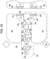
- FIG. 10 An alternative embodiment of the invention is shown in FIG. 10 . While the same basic fabrication steps and techniques discussed above in relation to FIGs. 2 - 9 can be used to form the pixel 200 (defined by dotted-line) shown in FIG. 10 , the features and elements of the pixel 200 are configured differently with respect to each other when compared to the layout of the pixel 100 of FIG. 2 .
- FIG. 10 shows the pixel 200 configuration in an array of like pixels.
- pixel 200 shares part of its circuitry components, i.e., gates 208, 210, 212, with other adjacent pixels, e.g., 300, 400, and 500, which are part of an array of similarly arranged pixels.
- Each pixel 200, 300, and 400 has an individual photodiode; e.g., photodiode 204 of pixel 200.
- the sharing of circuitry makes for a much more dense imager array.
- the transfer gate 206 is again configured so as not to overlap STI regions 236. As shown in FIG. 10 , implant regions 239 of p-type ions are provided between the STI regions 236 and the transfer gate 206.
- the transfer gate 206 is angled with respect to the photodiode 204, as shown in FIG. 10 .
- the term "angled" means that a portion of the transfer gate 206 is positioned across a corner of the photodiode 204 as opposed to across its length or width, as discussed above in relation to the embodiment shown in FIG. 2 .
- This preferred angled geometry of the transfer gate 206 allows for an efficient layout of the transfer gate 206.
- this angled layout is also beneficial in maximizing the fill factor of the pixel 200 by maximizing the area of the photodiode 204.
- the remaining pixel components are shared by the adjacent pixels 200 and 400. These components include the floating diffusion region 214, which serves as a common storage node for the pixels 200 and 400.
- a reset gate 208 is located proximate the floating diffusion region 214.
- a source/drain region 216 is located on a second side of the reset gate 208 opposite the floating diffusion region 214 and is capable of receiving a supply voltage (V aa ).
- the floating diffusion region 214 is also electrically connected to the source follower gate 210 (connection not shown), which has a source/drain 218.
- the source follower transistor having gate 210 outputs a voltage output signal from the floating diffusion region 214 to the row select transistor having gate 212.
- the row select transistor gate 212 has a source/drain 220 adjacent thereto for selectively reading out the pixel signal to a column line (not shown).
- a capacitor 238 is electrically connected (not shown) to the floating diffusion region 214.
- the capacitor 238 can increase the charge storage capacity of the floating diffusion region 214.
- the transistor gates 206, 208, 210, and 212, floating diffusion region 214, and source/drain regions 216, 218, and 220, have contacts 222, 224, 226, 228, 230, 232, and 234, respectively thereto.
- FIG. 11 illustrates an exemplary imager 700 that may utilize any embodiment of the invention.
- the imager 700 has a pixel array 705 comprising pixels constructed as described above with respect to, e.g., FIGs. 2 and 10 , or using other pixel architectures within the scope of the invention.
- Row lines are selectively activated by a row driver 710 in response to row address decoder 720.
- a column driver 760 and column address decoder 770 are also included in the imager 700.
- the imager 700 is operated by the timing and control circuit 750, which controls the address decoders 720, 770.
- the control circuit 750 also controls the row and column driver circuitry 710, 760 in accordance with an embodiment of the invention.
- a sample and hold circuit 761 associated with the column driver 760 reads a pixel reset signal V rst and a pixel image signal V sig for selected pixels.
- a differential signal (V rst -V sig ) is amplified by differential amplifier 762 for each pixel and is digitized by analog-to-digital converter 775 (ADC).
- ADC analog-to-digital converter 775
- the analog-to-digital converter 775 supplies the digitized pixel signals to an image processor 780 which forms a digital image.
- the image processor 780 may also determine the gain setting of the imager 700, which can be used to set the level of the voltage applied to the pixels transfer gates.
- FIG. 12 shows a system 1000, a typical processor system modified to include an imaging device 1008 (such as an imager 700 as shown in FIG. 11 with pixels 100 or 200 as illustrated in FIGs. 2 and 10 ) of the invention.
- the processor system 1000 is exemplary of a system having digital circuits that could include image sensor devices. Without being limiting, such a system could include a computer system, camera system, scanner, machine vision, vehicle navigation, video phone, surveillance system, auto focus system, star tracker system, motion detection system, image stabilization system, and data compression system, and other systems employing an imager.
- System 1000 for example a camera system, generally comprises a central processing unit (CPU) 1002, such as a microprocessor, that communicates with an input/output (I/O) device 1006 over a bus 1020.
- Imaging device 1008 also communicates with the CPU 1002 over the bus 1020.
- the processor-based system 1000 also includes random access memory (RAM)1004, and can include removable memory 1014, such as flash memory, which also communicate with the CPU 1002 over the bus 1020.
- the imaging device 1008 may be combined with a processor, such as a CPU, digital signal processor, or microprocessor, with or without memory storage on a single integrated circuit or on a different chip than the processor.
Landscapes
- Solid State Image Pick-Up Elements (AREA)
- Transforming Light Signals Into Electric Signals (AREA)
Claims (13)
- Dispositif imageur comprenant un substrat semi-conducteur (102) et un pixel d'imageur (10), le pixel d'imageur comprenant :une région active (104, 114, 116, 118, 120) formée à partir de parties dopées du substrat semi-conducteur (102), la région active comprenant un dispositif de photoconversion (104) et une région de stockage de charge (114) ;un circuit (106, 124, 110, 128) configuré pour recevoir une charge du dispositif de photoconversion (104) et délivrer une tension représentative de la charge, le circuit comprenant une grille de transistor de transfert (106), la grille de transistor de transfert (106) étant configurée pour transférer la charge du dispositif de photoconversion (104) à la région de stockage de charge (114) ;une région d'isolation par tranchée peu profonde (136) formée à partir d'oxyde dans le substrat semi-conducteur (102), qui entoure la région active et le circuit,caractérisé en ce quela grille de transistor de transfert (106) est configurée de manière à ne chevaucher aucune partie de la région d'isolation par tranchée peu profonde (136) ; etle pixel d'imageur comprend en outre des régions d'implant (139) dans la région active, les régions d'implant (139) étant interposées entre la grille de transistor de transfert (106) et la région d'isolation par tranchée peu profonde (136), lorsqu'elles sont vues de dessus, le long de régions frontières entre la grille de transistor de transfert (106) et la région d'isolation par tranchée peu profonde (136), et les régions d'implant (139) étant configurées pour empêcher que ladite charge ne soit transférée du dispositif de photoconversion (104) à la région de stockage de charge (114) le long des côtés de la grille de transistor de transfert (106), de manière à limiter le transfert de charge à une région de canal (115) sous la grille de transistor de transfert (106).
- Dispositif imageur selon la revendication 1, dans lequel le circuit comprend en outre un transistor de réinitialisation (108), un transistor suiveur de source (110) et un transistor de sélection de rangée (112).
- Dispositif imageur selon la revendication 1, dans lequel au moins une partie du circuit est partagée avec un pixel d'imageur adjacent (10).
- Dispositif imageur selon la revendication 1, dans lequel le dispositif de photoconversion (104) est une photodiode.
- Dispositif imageur selon la revendication 1, dans lequel le pixel est un pixel CMOS.
- Dispositif imageur selon la revendication 1, dans lequel le dispositif de photoconversion (104) est une photodiode dans le substrat semi-conducteur (102), le pixel d'imageur comprenant en outre :une grille de réinitialisation (108) configurée pour réinitialiser la région de stockage de charge (114) ;une grille suiveuse de source (110) configurée pour recevoir la charge de la région de stockage de charge (114) ; etune grille de sélection de rangée (112) configurée pour coupler la grille suiveuse de source (110) à une ligne de sortie, dans lequella région d'isolation par tranchée peu profonde (136) entoure la photodiode, la grille de transfert (106), la grille de réinitialisation (108), la grille suiveuse de source (110) et la grille de sélection de rangée (112).
- Dispositif imageur selon la revendication 6, dans lequel les régions d'implant (139) comprennent un dopant de type p.
- Dispositif imageur selon la revendication 6, dans lequel au moins l'une de la grille de réinitialisation (108), de la grille suiveuse de source (110), de la grille de sélection de rangée (112) et de la région de stockage de charge (114) est partagée avec un pixel adjacent.
- Procédé pour former un pixel d'imageur (10), consistant à :fournir un substrat semi-conducteur (102) ;former une région d'isolation par tranchée peu profonde (136) et une région active (104, 114, 116, 118, 120) dans le substrat semi-conducteur (102), la région d'isolation par tranchée peu profonde (136) comprenant une région d'oxyde formée dans le substrat semi-conducteur (102) et la région active comprenant une région de semi-conducteur dopé ;former un dispositif de photoconversion (104) dans la région active, la région active étant entourée par la région d'isolation par tranchée peu profonde (136) ;former une région de stockage de charge (114) dans la région active dans le substrat semi-conducteur (102) ;former une grille de transistor de transfert (106) à proximité du dispositif de photoconversion (104), la grille de transistor de transfert (106) étant configurée pour transférer la charge du dispositif de photoconversion (104) à la région de stockage de charge (114) ;caractérisé en ce que la grille de transistor de transfert (106) est configurée de manière à ne pas chevaucher la région d'isolation par tranchée peu profonde (136) et que le procédé consiste en outre à former des régions d'implant (139) dans la région active (104, 114, 116, 118, 120), interposées entre la grille de transistor de transfert (106) et la région d'isolation par tranchée peu profonde (136), lorsqu'elles sont vues de dessus, le long de régions frontières entre la grille de transistor de transfert (106) et l'isolation par tranchée peu profonde (136), lesdites régions d'implant (139) étant configurées pour empêcher que ladite charge ne soit transférée du dispositif de photoconversion (104) à la région de stockage de charge (114) le long des côtés de la grille de transistor de transfert (106) de manière à limiter le transfert de charge à une région de canal (115) sous la grille de transistor de transfert (106).
- Procédé selon la revendication 9, comprenant en outre l'étape consistant à former un transistor de réinitialisation (108), un transistor suiveur de source (110) et un transistor de sélection de rangée (112) à proximité du dispositif de photoconversion (104).
- Procédé selon la revendication 10, comprenant en outre l'étape consistant à former un deuxième dispositif de photoconversion (104) qui partage au moins l'un du transistor de réinitialisation (108), du transistor suiveur de source (110) et du transistor de sélection de rangée (112).
- Procédé selon la revendication 9, dans lequel le dispositif de photoconversion (104) est une photodiode.
- Procédé selon la revendication 9, dans lequel le pixel (10) est un pixel CMOS.
Applications Claiming Priority (2)
| Application Number | Priority Date | Filing Date | Title |
|---|---|---|---|
| US11/178,798 US7449736B2 (en) | 2005-07-12 | 2005-07-12 | Pixel with transfer gate with no isolation edge |
| PCT/US2006/026278 WO2007008552A2 (fr) | 2005-07-12 | 2006-07-07 | Element d'image a grille de transfert sans arete d'isolation |
Publications (2)
| Publication Number | Publication Date |
|---|---|
| EP1908109A2 EP1908109A2 (fr) | 2008-04-09 |
| EP1908109B1 true EP1908109B1 (fr) | 2018-06-27 |
Family
ID=37387242
Family Applications (1)
| Application Number | Title | Priority Date | Filing Date |
|---|---|---|---|
| EP06786435.5A Not-in-force EP1908109B1 (fr) | 2005-07-12 | 2006-07-07 | Element d'image a grille de transfert sans arete d'isolation |
Country Status (7)
| Country | Link |
|---|---|
| US (2) | US7449736B2 (fr) |
| EP (1) | EP1908109B1 (fr) |
| JP (1) | JP2009501446A (fr) |
| KR (1) | KR101005421B1 (fr) |
| CN (1) | CN101258599B (fr) |
| TW (1) | TWI308795B (fr) |
| WO (1) | WO2007008552A2 (fr) |
Families Citing this family (12)
| Publication number | Priority date | Publication date | Assignee | Title |
|---|---|---|---|---|
| JP4420039B2 (ja) * | 2007-02-16 | 2010-02-24 | ソニー株式会社 | 固体撮像装置 |
| US7642580B2 (en) * | 2007-06-20 | 2010-01-05 | Apitina Imaging Corporation | Imager pixel structure and circuit |
| JP4991418B2 (ja) * | 2007-07-06 | 2012-08-01 | 株式会社東芝 | 固体撮像装置 |
| JP2009038263A (ja) * | 2007-08-02 | 2009-02-19 | Sharp Corp | 固体撮像素子および電子情報機器 |
| JP5292787B2 (ja) | 2007-11-30 | 2013-09-18 | ソニー株式会社 | 固体撮像装置及びカメラ |
| KR100937673B1 (ko) * | 2007-12-28 | 2010-01-19 | 주식회사 동부하이텍 | Cmos 이미지 센서 |
| CN103000651B (zh) * | 2012-12-24 | 2017-02-22 | 上海华虹宏力半导体制造有限公司 | Cmos图像传感器的形成方法 |
| JP2015115391A (ja) * | 2013-12-10 | 2015-06-22 | 株式会社ニコン | 撮像素子、撮像素子の製造方法、及び電子機器 |
| US10165210B1 (en) * | 2017-12-22 | 2018-12-25 | Omnivision Technologies, Inc. | Bitline settling improvement by using dummy pixels for clamp |
| JP6601520B2 (ja) * | 2018-03-12 | 2019-11-06 | 株式会社ニコン | 撮像素子、撮像素子の製造方法、及び電子機器 |
| CN112542474B (zh) * | 2019-09-23 | 2025-03-11 | 格科微电子(上海)有限公司 | Cmos图像传感器的形成方法及cmos图像传感器 |
| WO2022104658A1 (fr) * | 2020-11-19 | 2022-05-27 | Huawei Technologies Co., Ltd. | Dispositif d'imagerie à semi-conducteur |
Family Cites Families (20)
| Publication number | Priority date | Publication date | Assignee | Title |
|---|---|---|---|---|
| US6160281A (en) | 1997-02-28 | 2000-12-12 | Eastman Kodak Company | Active pixel sensor with inter-pixel function sharing |
| US6107655A (en) | 1997-08-15 | 2000-08-22 | Eastman Kodak Company | Active pixel image sensor with shared amplifier read-out |
| US6140630A (en) * | 1998-10-14 | 2000-10-31 | Micron Technology, Inc. | Vcc pump for CMOS imagers |
| US6376868B1 (en) * | 1999-06-15 | 2002-04-23 | Micron Technology, Inc. | Multi-layered gate for a CMOS imager |
| US6310366B1 (en) * | 1999-06-16 | 2001-10-30 | Micron Technology, Inc. | Retrograde well structure for a CMOS imager |
| US6326652B1 (en) * | 1999-06-18 | 2001-12-04 | Micron Technology, Inc., | CMOS imager with a self-aligned buried contact |
| US6204524B1 (en) * | 1999-07-14 | 2001-03-20 | Micron Technology, Inc. | CMOS imager with storage capacitor |
| US6333205B1 (en) * | 1999-08-16 | 2001-12-25 | Micron Technology, Inc. | CMOS imager with selectively silicided gates |
| US6462365B1 (en) * | 2001-11-06 | 2002-10-08 | Omnivision Technologies, Inc. | Active pixel having reduced dark current in a CMOS image sensor |
| KR100494030B1 (ko) * | 2002-01-10 | 2005-06-10 | 매그나칩 반도체 유한회사 | 이미지센서 및 그 제조 방법 |
| US7232712B2 (en) * | 2003-10-28 | 2007-06-19 | Dongbu Electronics Co., Ltd. | CMOS image sensor and method for fabricating the same |
| US7354789B2 (en) * | 2003-11-04 | 2008-04-08 | Dongbu Electronics Co., Ltd. | CMOS image sensor and method for fabricating the same |
| US7205584B2 (en) * | 2003-12-22 | 2007-04-17 | Micron Technology, Inc. | Image sensor for reduced dark current |
| KR100619396B1 (ko) | 2003-12-31 | 2006-09-11 | 동부일렉트로닉스 주식회사 | 시모스 이미지 센서 및 그 제조방법 |
| US20060255380A1 (en) * | 2005-05-10 | 2006-11-16 | Nan-Yi Lee | CMOS image sensor |
| US7145122B2 (en) * | 2004-06-14 | 2006-12-05 | Omnivision Technologies, Inc. | Imaging sensor using asymmetric transfer transistor |
| US7667250B2 (en) * | 2004-07-16 | 2010-02-23 | Aptina Imaging Corporation | Vertical gate device for an image sensor and method of forming the same |
| US7271025B2 (en) * | 2005-07-12 | 2007-09-18 | Micron Technology, Inc. | Image sensor with SOI substrate |
| US7511323B2 (en) * | 2005-08-11 | 2009-03-31 | Aptina Imaging Corporation | Pixel cells in a honeycomb arrangement |
| JP4991418B2 (ja) * | 2007-07-06 | 2012-08-01 | 株式会社東芝 | 固体撮像装置 |
-
2005
- 2005-07-12 US US11/178,798 patent/US7449736B2/en active Active
-
2006
- 2006-07-07 WO PCT/US2006/026278 patent/WO2007008552A2/fr not_active Ceased
- 2006-07-07 CN CN2006800328700A patent/CN101258599B/zh not_active Expired - Fee Related
- 2006-07-07 KR KR1020087002939A patent/KR101005421B1/ko active Active
- 2006-07-07 EP EP06786435.5A patent/EP1908109B1/fr not_active Not-in-force
- 2006-07-07 JP JP2008521433A patent/JP2009501446A/ja not_active Withdrawn
- 2006-07-12 TW TW095125371A patent/TWI308795B/zh active
-
2008
- 2008-10-10 US US12/249,723 patent/US7829922B2/en not_active Expired - Lifetime
Non-Patent Citations (1)
| Title |
|---|
| None * |
Also Published As
| Publication number | Publication date |
|---|---|
| WO2007008552A2 (fr) | 2007-01-18 |
| CN101258599B (zh) | 2010-06-16 |
| KR20080027380A (ko) | 2008-03-26 |
| WO2007008552A3 (fr) | 2007-04-26 |
| KR101005421B1 (ko) | 2010-12-30 |
| US7829922B2 (en) | 2010-11-09 |
| TWI308795B (en) | 2009-04-11 |
| EP1908109A2 (fr) | 2008-04-09 |
| JP2009501446A (ja) | 2009-01-15 |
| US20070012917A1 (en) | 2007-01-18 |
| TW200715540A (en) | 2007-04-16 |
| CN101258599A (zh) | 2008-09-03 |
| US7449736B2 (en) | 2008-11-11 |
| US20090090945A1 (en) | 2009-04-09 |
Similar Documents
| Publication | Publication Date | Title |
|---|---|---|
| US7829922B2 (en) | Pixel with transfer gate with no isolation edge | |
| EP1935021B1 (fr) | Region d'isolation implantee pour pixels d'imageur | |
| US7619266B2 (en) | Image sensor with improved surface depletion | |
| US6232626B1 (en) | Trench photosensor for a CMOS imager | |
| US7115923B2 (en) | Imaging with gate controlled charge storage | |
| EP1668701B1 (fr) | CAPTEUR D'IMAGE COMPRENANT UNE DIODE DE DIFFUSION FLOTTANTE A BROCHES et son procédé de fabrication | |
| KR100812792B1 (ko) | 씨모스 이미지 센서 및 제조 방법 | |
| US6967121B2 (en) | Buried channel CMOS imager and method of forming same | |
| US7250321B2 (en) | Method of forming a photosensor | |
| US6465786B1 (en) | Deep infrared photodiode for a CMOS imager | |
| US8211732B2 (en) | Image sensor with raised photosensitive elements | |
| US20100079645A1 (en) | Cmos imager and system with selectively silicided gates | |
| US20060255381A1 (en) | Pixel with gate contacts over active region and method of forming same | |
| US8105858B2 (en) | CMOS imager having a nitride dielectric |
Legal Events
| Date | Code | Title | Description |
|---|---|---|---|
| PUAI | Public reference made under article 153(3) epc to a published international application that has entered the european phase |
Free format text: ORIGINAL CODE: 0009012 |
|
| 17P | Request for examination filed |
Effective date: 20080204 |
|
| AK | Designated contracting states |
Kind code of ref document: A2 Designated state(s): AT BE BG CH CY CZ DE DK EE ES FI FR GB GR HU IE IS IT LI LT LU LV MC NL PL PT RO SE SI SK TR |
|
| 17Q | First examination report despatched |
Effective date: 20080613 |
|
| RAP1 | Party data changed (applicant data changed or rights of an application transferred) |
Owner name: APTINA IMAGING CORPORATION |
|
| DAX | Request for extension of the european patent (deleted) | ||
| RAP1 | Party data changed (applicant data changed or rights of an application transferred) |
Owner name: APTINA IMAGING CORPORATION |
|
| STAA | Information on the status of an ep patent application or granted ep patent |
Free format text: STATUS: EXAMINATION IS IN PROGRESS |
|
| GRAP | Despatch of communication of intention to grant a patent |
Free format text: ORIGINAL CODE: EPIDOSNIGR1 |
|
| STAA | Information on the status of an ep patent application or granted ep patent |
Free format text: STATUS: GRANT OF PATENT IS INTENDED |
|
| INTG | Intention to grant announced |
Effective date: 20180201 |
|
| GRAS | Grant fee paid |
Free format text: ORIGINAL CODE: EPIDOSNIGR3 |
|
| GRAA | (expected) grant |
Free format text: ORIGINAL CODE: 0009210 |
|
| STAA | Information on the status of an ep patent application or granted ep patent |
Free format text: STATUS: THE PATENT HAS BEEN GRANTED |
|
| AK | Designated contracting states |
Kind code of ref document: B1 Designated state(s): AT BE BG CH CY CZ DE DK EE ES FI FR GB GR HU IE IS IT LI LT LU LV MC NL PL PT RO SE SI SK TR |
|
| REG | Reference to a national code |
Ref country code: GB Ref legal event code: FG4D |
|
| REG | Reference to a national code |
Ref country code: AT Ref legal event code: REF Ref document number: 1013060 Country of ref document: AT Kind code of ref document: T Effective date: 20180715 |
|
| REG | Reference to a national code |
Ref country code: IE Ref legal event code: FG4D |
|
| REG | Reference to a national code |
Ref country code: DE Ref legal event code: R096 Ref document number: 602006055700 Country of ref document: DE |
|
| PG25 | Lapsed in a contracting state [announced via postgrant information from national office to epo] |
Ref country code: BG Free format text: LAPSE BECAUSE OF FAILURE TO SUBMIT A TRANSLATION OF THE DESCRIPTION OR TO PAY THE FEE WITHIN THE PRESCRIBED TIME-LIMIT Effective date: 20180927 Ref country code: FI Free format text: LAPSE BECAUSE OF FAILURE TO SUBMIT A TRANSLATION OF THE DESCRIPTION OR TO PAY THE FEE WITHIN THE PRESCRIBED TIME-LIMIT Effective date: 20180627 Ref country code: SE Free format text: LAPSE BECAUSE OF FAILURE TO SUBMIT A TRANSLATION OF THE DESCRIPTION OR TO PAY THE FEE WITHIN THE PRESCRIBED TIME-LIMIT Effective date: 20180627 Ref country code: LT Free format text: LAPSE BECAUSE OF FAILURE TO SUBMIT A TRANSLATION OF THE DESCRIPTION OR TO PAY THE FEE WITHIN THE PRESCRIBED TIME-LIMIT Effective date: 20180627 |
|
| REG | Reference to a national code |
Ref country code: NL Ref legal event code: MP Effective date: 20180627 |
|
| REG | Reference to a national code |
Ref country code: LT Ref legal event code: MG4D |
|
| PG25 | Lapsed in a contracting state [announced via postgrant information from national office to epo] |
Ref country code: LV Free format text: LAPSE BECAUSE OF FAILURE TO SUBMIT A TRANSLATION OF THE DESCRIPTION OR TO PAY THE FEE WITHIN THE PRESCRIBED TIME-LIMIT Effective date: 20180627 Ref country code: GR Free format text: LAPSE BECAUSE OF FAILURE TO SUBMIT A TRANSLATION OF THE DESCRIPTION OR TO PAY THE FEE WITHIN THE PRESCRIBED TIME-LIMIT Effective date: 20180928 |
|
| REG | Reference to a national code |
Ref country code: AT Ref legal event code: MK05 Ref document number: 1013060 Country of ref document: AT Kind code of ref document: T Effective date: 20180627 |
|
| PG25 | Lapsed in a contracting state [announced via postgrant information from national office to epo] |
Ref country code: NL Free format text: LAPSE BECAUSE OF FAILURE TO SUBMIT A TRANSLATION OF THE DESCRIPTION OR TO PAY THE FEE WITHIN THE PRESCRIBED TIME-LIMIT Effective date: 20180627 |
|
| PG25 | Lapsed in a contracting state [announced via postgrant information from national office to epo] |
Ref country code: EE Free format text: LAPSE BECAUSE OF FAILURE TO SUBMIT A TRANSLATION OF THE DESCRIPTION OR TO PAY THE FEE WITHIN THE PRESCRIBED TIME-LIMIT Effective date: 20180627 Ref country code: PL Free format text: LAPSE BECAUSE OF FAILURE TO SUBMIT A TRANSLATION OF THE DESCRIPTION OR TO PAY THE FEE WITHIN THE PRESCRIBED TIME-LIMIT Effective date: 20180627 Ref country code: SK Free format text: LAPSE BECAUSE OF FAILURE TO SUBMIT A TRANSLATION OF THE DESCRIPTION OR TO PAY THE FEE WITHIN THE PRESCRIBED TIME-LIMIT Effective date: 20180627 Ref country code: RO Free format text: LAPSE BECAUSE OF FAILURE TO SUBMIT A TRANSLATION OF THE DESCRIPTION OR TO PAY THE FEE WITHIN THE PRESCRIBED TIME-LIMIT Effective date: 20180627 Ref country code: CZ Free format text: LAPSE BECAUSE OF FAILURE TO SUBMIT A TRANSLATION OF THE DESCRIPTION OR TO PAY THE FEE WITHIN THE PRESCRIBED TIME-LIMIT Effective date: 20180627 Ref country code: AT Free format text: LAPSE BECAUSE OF FAILURE TO SUBMIT A TRANSLATION OF THE DESCRIPTION OR TO PAY THE FEE WITHIN THE PRESCRIBED TIME-LIMIT Effective date: 20180627 Ref country code: IS Free format text: LAPSE BECAUSE OF FAILURE TO SUBMIT A TRANSLATION OF THE DESCRIPTION OR TO PAY THE FEE WITHIN THE PRESCRIBED TIME-LIMIT Effective date: 20181027 |
|
| PG25 | Lapsed in a contracting state [announced via postgrant information from national office to epo] |
Ref country code: ES Free format text: LAPSE BECAUSE OF FAILURE TO SUBMIT A TRANSLATION OF THE DESCRIPTION OR TO PAY THE FEE WITHIN THE PRESCRIBED TIME-LIMIT Effective date: 20180627 |
|
| REG | Reference to a national code |
Ref country code: CH Ref legal event code: PL |
|
| REG | Reference to a national code |
Ref country code: DE Ref legal event code: R097 Ref document number: 602006055700 Country of ref document: DE |
|
| PG25 | Lapsed in a contracting state [announced via postgrant information from national office to epo] |
Ref country code: LU Free format text: LAPSE BECAUSE OF NON-PAYMENT OF DUE FEES Effective date: 20180707 Ref country code: MC Free format text: LAPSE BECAUSE OF FAILURE TO SUBMIT A TRANSLATION OF THE DESCRIPTION OR TO PAY THE FEE WITHIN THE PRESCRIBED TIME-LIMIT Effective date: 20180627 |
|
| REG | Reference to a national code |
Ref country code: BE Ref legal event code: MM Effective date: 20180731 |
|
| REG | Reference to a national code |
Ref country code: IE Ref legal event code: MM4A |
|
| PG25 | Lapsed in a contracting state [announced via postgrant information from national office to epo] |
Ref country code: LI Free format text: LAPSE BECAUSE OF NON-PAYMENT OF DUE FEES Effective date: 20180731 Ref country code: CH Free format text: LAPSE BECAUSE OF NON-PAYMENT OF DUE FEES Effective date: 20180731 Ref country code: IE Free format text: LAPSE BECAUSE OF NON-PAYMENT OF DUE FEES Effective date: 20180707 |
|
| PLBE | No opposition filed within time limit |
Free format text: ORIGINAL CODE: 0009261 |
|
| STAA | Information on the status of an ep patent application or granted ep patent |
Free format text: STATUS: NO OPPOSITION FILED WITHIN TIME LIMIT |
|
| PG25 | Lapsed in a contracting state [announced via postgrant information from national office to epo] |
Ref country code: BE Free format text: LAPSE BECAUSE OF NON-PAYMENT OF DUE FEES Effective date: 20180731 Ref country code: DK Free format text: LAPSE BECAUSE OF FAILURE TO SUBMIT A TRANSLATION OF THE DESCRIPTION OR TO PAY THE FEE WITHIN THE PRESCRIBED TIME-LIMIT Effective date: 20180627 |
|
| 26N | No opposition filed |
Effective date: 20190328 |
|
| PG25 | Lapsed in a contracting state [announced via postgrant information from national office to epo] |
Ref country code: FR Free format text: LAPSE BECAUSE OF NON-PAYMENT OF DUE FEES Effective date: 20180827 Ref country code: SI Free format text: LAPSE BECAUSE OF FAILURE TO SUBMIT A TRANSLATION OF THE DESCRIPTION OR TO PAY THE FEE WITHIN THE PRESCRIBED TIME-LIMIT Effective date: 20180627 |
|
| PG25 | Lapsed in a contracting state [announced via postgrant information from national office to epo] |
Ref country code: TR Free format text: LAPSE BECAUSE OF FAILURE TO SUBMIT A TRANSLATION OF THE DESCRIPTION OR TO PAY THE FEE WITHIN THE PRESCRIBED TIME-LIMIT Effective date: 20180627 |
|
| PG25 | Lapsed in a contracting state [announced via postgrant information from national office to epo] |
Ref country code: PT Free format text: LAPSE BECAUSE OF FAILURE TO SUBMIT A TRANSLATION OF THE DESCRIPTION OR TO PAY THE FEE WITHIN THE PRESCRIBED TIME-LIMIT Effective date: 20180627 Ref country code: HU Free format text: LAPSE BECAUSE OF FAILURE TO SUBMIT A TRANSLATION OF THE DESCRIPTION OR TO PAY THE FEE WITHIN THE PRESCRIBED TIME-LIMIT; INVALID AB INITIO Effective date: 20060707 |
|
| PG25 | Lapsed in a contracting state [announced via postgrant information from national office to epo] |
Ref country code: CY Free format text: LAPSE BECAUSE OF FAILURE TO SUBMIT A TRANSLATION OF THE DESCRIPTION OR TO PAY THE FEE WITHIN THE PRESCRIBED TIME-LIMIT Effective date: 20180627 |
|
| PGFP | Annual fee paid to national office [announced via postgrant information from national office to epo] |
Ref country code: GB Payment date: 20200624 Year of fee payment: 15 |
|
| PGFP | Annual fee paid to national office [announced via postgrant information from national office to epo] |
Ref country code: DE Payment date: 20200622 Year of fee payment: 15 |
|
| PGFP | Annual fee paid to national office [announced via postgrant information from national office to epo] |
Ref country code: IT Payment date: 20200622 Year of fee payment: 15 |
|
| REG | Reference to a national code |
Ref country code: DE Ref legal event code: R119 Ref document number: 602006055700 Country of ref document: DE |
|
| GBPC | Gb: european patent ceased through non-payment of renewal fee |
Effective date: 20210707 |
|
| PG25 | Lapsed in a contracting state [announced via postgrant information from national office to epo] |
Ref country code: GB Free format text: LAPSE BECAUSE OF NON-PAYMENT OF DUE FEES Effective date: 20210707 Ref country code: DE Free format text: LAPSE BECAUSE OF NON-PAYMENT OF DUE FEES Effective date: 20220201 |
|
| PG25 | Lapsed in a contracting state [announced via postgrant information from national office to epo] |
Ref country code: IT Free format text: LAPSE BECAUSE OF NON-PAYMENT OF DUE FEES Effective date: 20210707 |