EP1906452A1 - Semiconductor device and method for manufacturing same - Google Patents
Semiconductor device and method for manufacturing same Download PDFInfo
- Publication number
- EP1906452A1 EP1906452A1 EP06729669A EP06729669A EP1906452A1 EP 1906452 A1 EP1906452 A1 EP 1906452A1 EP 06729669 A EP06729669 A EP 06729669A EP 06729669 A EP06729669 A EP 06729669A EP 1906452 A1 EP1906452 A1 EP 1906452A1
- Authority
- EP
- European Patent Office
- Prior art keywords
- electrode layer
- cell
- region
- igbt
- layer
- Prior art date
- Legal status (The legal status is an assumption and is not a legal conclusion. Google has not performed a legal analysis and makes no representation as to the accuracy of the status listed.)
- Granted
Links
Images


Classifications
-
- H—ELECTRICITY
- H10—SEMICONDUCTOR DEVICES; ELECTRIC SOLID-STATE DEVICES NOT OTHERWISE PROVIDED FOR
- H10W—GENERIC PACKAGES, INTERCONNECTIONS, CONNECTORS OR OTHER CONSTRUCTIONAL DETAILS OF DEVICES COVERED BY CLASS H10
- H10W90/00—Package configurations
-
- H—ELECTRICITY
- H10—SEMICONDUCTOR DEVICES; ELECTRIC SOLID-STATE DEVICES NOT OTHERWISE PROVIDED FOR
- H10D—INORGANIC ELECTRIC SEMICONDUCTOR DEVICES
- H10D12/00—Bipolar devices controlled by the field effect, e.g. insulated-gate bipolar transistors [IGBT]
- H10D12/411—Insulated-gate bipolar transistors [IGBT]
- H10D12/441—Vertical IGBTs
-
- H—ELECTRICITY
- H10—SEMICONDUCTOR DEVICES; ELECTRIC SOLID-STATE DEVICES NOT OTHERWISE PROVIDED FOR
- H10W—GENERIC PACKAGES, INTERCONNECTIONS, CONNECTORS OR OTHER CONSTRUCTIONAL DETAILS OF DEVICES COVERED BY CLASS H10
- H10W72/00—Interconnections or connectors in packages
- H10W72/071—Connecting or disconnecting
- H10W72/073—Connecting or disconnecting of die-attach connectors
-
- H—ELECTRICITY
- H10—SEMICONDUCTOR DEVICES; ELECTRIC SOLID-STATE DEVICES NOT OTHERWISE PROVIDED FOR
- H10W—GENERIC PACKAGES, INTERCONNECTIONS, CONNECTORS OR OTHER CONSTRUCTIONAL DETAILS OF DEVICES COVERED BY CLASS H10
- H10W72/00—Interconnections or connectors in packages
- H10W72/071—Connecting or disconnecting
- H10W72/075—Connecting or disconnecting of bond wires
-
- H—ELECTRICITY
- H10—SEMICONDUCTOR DEVICES; ELECTRIC SOLID-STATE DEVICES NOT OTHERWISE PROVIDED FOR
- H10W—GENERIC PACKAGES, INTERCONNECTIONS, CONNECTORS OR OTHER CONSTRUCTIONAL DETAILS OF DEVICES COVERED BY CLASS H10
- H10W72/00—Interconnections or connectors in packages
- H10W72/50—Bond wires
- H10W72/531—Shapes of wire connectors
- H10W72/536—Shapes of wire connectors the connected ends being ball-shaped
-
- H—ELECTRICITY
- H10—SEMICONDUCTOR DEVICES; ELECTRIC SOLID-STATE DEVICES NOT OTHERWISE PROVIDED FOR
- H10W—GENERIC PACKAGES, INTERCONNECTIONS, CONNECTORS OR OTHER CONSTRUCTIONAL DETAILS OF DEVICES COVERED BY CLASS H10
- H10W72/00—Interconnections or connectors in packages
- H10W72/50—Bond wires
- H10W72/541—Dispositions of bond wires
- H10W72/5449—Dispositions of bond wires not being orthogonal to a side surface of the chip, e.g. fan-out arrangements
-
- H—ELECTRICITY
- H10—SEMICONDUCTOR DEVICES; ELECTRIC SOLID-STATE DEVICES NOT OTHERWISE PROVIDED FOR
- H10W—GENERIC PACKAGES, INTERCONNECTIONS, CONNECTORS OR OTHER CONSTRUCTIONAL DETAILS OF DEVICES COVERED BY CLASS H10
- H10W72/00—Interconnections or connectors in packages
- H10W72/50—Bond wires
- H10W72/541—Dispositions of bond wires
- H10W72/547—Dispositions of multiple bond wires
- H10W72/5473—Dispositions of multiple bond wires multiple bond wires connected to a common bond pad
-
- H—ELECTRICITY
- H10—SEMICONDUCTOR DEVICES; ELECTRIC SOLID-STATE DEVICES NOT OTHERWISE PROVIDED FOR
- H10W—GENERIC PACKAGES, INTERCONNECTIONS, CONNECTORS OR OTHER CONSTRUCTIONAL DETAILS OF DEVICES COVERED BY CLASS H10
- H10W72/00—Interconnections or connectors in packages
- H10W72/50—Bond wires
- H10W72/541—Dispositions of bond wires
- H10W72/547—Dispositions of multiple bond wires
- H10W72/5475—Dispositions of multiple bond wires multiple bond wires connected to common bond pads at both ends of the wires
-
- H—ELECTRICITY
- H10—SEMICONDUCTOR DEVICES; ELECTRIC SOLID-STATE DEVICES NOT OTHERWISE PROVIDED FOR
- H10W—GENERIC PACKAGES, INTERCONNECTIONS, CONNECTORS OR OTHER CONSTRUCTIONAL DETAILS OF DEVICES COVERED BY CLASS H10
- H10W72/00—Interconnections or connectors in packages
- H10W72/50—Bond wires
- H10W72/551—Materials of bond wires
- H10W72/552—Materials of bond wires comprising metals or metalloids, e.g. silver
-
- H—ELECTRICITY
- H10—SEMICONDUCTOR DEVICES; ELECTRIC SOLID-STATE DEVICES NOT OTHERWISE PROVIDED FOR
- H10W—GENERIC PACKAGES, INTERCONNECTIONS, CONNECTORS OR OTHER CONSTRUCTIONAL DETAILS OF DEVICES COVERED BY CLASS H10
- H10W72/00—Interconnections or connectors in packages
- H10W72/50—Bond wires
- H10W72/551—Materials of bond wires
- H10W72/552—Materials of bond wires comprising metals or metalloids, e.g. silver
- H10W72/5522—Materials of bond wires comprising metals or metalloids, e.g. silver comprising gold [Au]
-
- H—ELECTRICITY
- H10—SEMICONDUCTOR DEVICES; ELECTRIC SOLID-STATE DEVICES NOT OTHERWISE PROVIDED FOR
- H10W—GENERIC PACKAGES, INTERCONNECTIONS, CONNECTORS OR OTHER CONSTRUCTIONAL DETAILS OF DEVICES COVERED BY CLASS H10
- H10W72/00—Interconnections or connectors in packages
- H10W72/50—Bond wires
- H10W72/551—Materials of bond wires
- H10W72/552—Materials of bond wires comprising metals or metalloids, e.g. silver
- H10W72/5524—Materials of bond wires comprising metals or metalloids, e.g. silver comprising aluminium [Al]
-
- H—ELECTRICITY
- H10—SEMICONDUCTOR DEVICES; ELECTRIC SOLID-STATE DEVICES NOT OTHERWISE PROVIDED FOR
- H10W—GENERIC PACKAGES, INTERCONNECTIONS, CONNECTORS OR OTHER CONSTRUCTIONAL DETAILS OF DEVICES COVERED BY CLASS H10
- H10W72/00—Interconnections or connectors in packages
- H10W72/50—Bond wires
- H10W72/551—Materials of bond wires
- H10W72/552—Materials of bond wires comprising metals or metalloids, e.g. silver
- H10W72/5525—Materials of bond wires comprising metals or metalloids, e.g. silver comprising copper [Cu]
-
- H—ELECTRICITY
- H10—SEMICONDUCTOR DEVICES; ELECTRIC SOLID-STATE DEVICES NOT OTHERWISE PROVIDED FOR
- H10W—GENERIC PACKAGES, INTERCONNECTIONS, CONNECTORS OR OTHER CONSTRUCTIONAL DETAILS OF DEVICES COVERED BY CLASS H10
- H10W72/00—Interconnections or connectors in packages
- H10W72/50—Bond wires
- H10W72/59—Bond pads specially adapted therefor
-
- H—ELECTRICITY
- H10—SEMICONDUCTOR DEVICES; ELECTRIC SOLID-STATE DEVICES NOT OTHERWISE PROVIDED FOR
- H10W—GENERIC PACKAGES, INTERCONNECTIONS, CONNECTORS OR OTHER CONSTRUCTIONAL DETAILS OF DEVICES COVERED BY CLASS H10
- H10W72/00—Interconnections or connectors in packages
- H10W72/851—Dispositions of multiple connectors or interconnections
- H10W72/874—On different surfaces
- H10W72/884—Die-attach connectors and bond wires
-
- H—ELECTRICITY
- H10—SEMICONDUCTOR DEVICES; ELECTRIC SOLID-STATE DEVICES NOT OTHERWISE PROVIDED FOR
- H10W—GENERIC PACKAGES, INTERCONNECTIONS, CONNECTORS OR OTHER CONSTRUCTIONAL DETAILS OF DEVICES COVERED BY CLASS H10
- H10W72/00—Interconnections or connectors in packages
- H10W72/90—Bond pads, in general
- H10W72/921—Structures or relative sizes of bond pads
- H10W72/926—Multiple bond pads having different sizes
-
- H—ELECTRICITY
- H10—SEMICONDUCTOR DEVICES; ELECTRIC SOLID-STATE DEVICES NOT OTHERWISE PROVIDED FOR
- H10W—GENERIC PACKAGES, INTERCONNECTIONS, CONNECTORS OR OTHER CONSTRUCTIONAL DETAILS OF DEVICES COVERED BY CLASS H10
- H10W72/00—Interconnections or connectors in packages
- H10W72/90—Bond pads, in general
- H10W72/931—Shapes of bond pads
- H10W72/932—Plan-view shape, i.e. in top view
-
- H—ELECTRICITY
- H10—SEMICONDUCTOR DEVICES; ELECTRIC SOLID-STATE DEVICES NOT OTHERWISE PROVIDED FOR
- H10W—GENERIC PACKAGES, INTERCONNECTIONS, CONNECTORS OR OTHER CONSTRUCTIONAL DETAILS OF DEVICES COVERED BY CLASS H10
- H10W72/00—Interconnections or connectors in packages
- H10W72/90—Bond pads, in general
- H10W72/931—Shapes of bond pads
- H10W72/934—Cross-sectional shape, i.e. in side view
-
- H—ELECTRICITY
- H10—SEMICONDUCTOR DEVICES; ELECTRIC SOLID-STATE DEVICES NOT OTHERWISE PROVIDED FOR
- H10W—GENERIC PACKAGES, INTERCONNECTIONS, CONNECTORS OR OTHER CONSTRUCTIONAL DETAILS OF DEVICES COVERED BY CLASS H10
- H10W72/00—Interconnections or connectors in packages
- H10W72/90—Bond pads, in general
- H10W72/951—Materials of bond pads
-
- H—ELECTRICITY
- H10—SEMICONDUCTOR DEVICES; ELECTRIC SOLID-STATE DEVICES NOT OTHERWISE PROVIDED FOR
- H10W—GENERIC PACKAGES, INTERCONNECTIONS, CONNECTORS OR OTHER CONSTRUCTIONAL DETAILS OF DEVICES COVERED BY CLASS H10
- H10W72/00—Interconnections or connectors in packages
- H10W72/90—Bond pads, in general
- H10W72/951—Materials of bond pads
- H10W72/952—Materials of bond pads comprising metals or metalloids, e.g. PbSn, Ag or Cu
-
- H—ELECTRICITY
- H10—SEMICONDUCTOR DEVICES; ELECTRIC SOLID-STATE DEVICES NOT OTHERWISE PROVIDED FOR
- H10W—GENERIC PACKAGES, INTERCONNECTIONS, CONNECTORS OR OTHER CONSTRUCTIONAL DETAILS OF DEVICES COVERED BY CLASS H10
- H10W72/00—Interconnections or connectors in packages
- H10W72/90—Bond pads, in general
- H10W72/981—Auxiliary members, e.g. spacers
- H10W72/983—Reinforcing structures, e.g. collars
-
- H—ELECTRICITY
- H10—SEMICONDUCTOR DEVICES; ELECTRIC SOLID-STATE DEVICES NOT OTHERWISE PROVIDED FOR
- H10W—GENERIC PACKAGES, INTERCONNECTIONS, CONNECTORS OR OTHER CONSTRUCTIONAL DETAILS OF DEVICES COVERED BY CLASS H10
- H10W74/00—Encapsulations, e.g. protective coatings
-
- H—ELECTRICITY
- H10—SEMICONDUCTOR DEVICES; ELECTRIC SOLID-STATE DEVICES NOT OTHERWISE PROVIDED FOR
- H10W—GENERIC PACKAGES, INTERCONNECTIONS, CONNECTORS OR OTHER CONSTRUCTIONAL DETAILS OF DEVICES COVERED BY CLASS H10
- H10W90/00—Package configurations
- H10W90/701—Package configurations characterised by the relative positions of pads or connectors relative to package parts
- H10W90/731—Package configurations characterised by the relative positions of pads or connectors relative to package parts of die-attach connectors
- H10W90/732—Package configurations characterised by the relative positions of pads or connectors relative to package parts of die-attach connectors between stacked chips
-
- H—ELECTRICITY
- H10—SEMICONDUCTOR DEVICES; ELECTRIC SOLID-STATE DEVICES NOT OTHERWISE PROVIDED FOR
- H10W—GENERIC PACKAGES, INTERCONNECTIONS, CONNECTORS OR OTHER CONSTRUCTIONAL DETAILS OF DEVICES COVERED BY CLASS H10
- H10W90/00—Package configurations
- H10W90/701—Package configurations characterised by the relative positions of pads or connectors relative to package parts
- H10W90/751—Package configurations characterised by the relative positions of pads or connectors relative to package parts of bond wires
- H10W90/753—Package configurations characterised by the relative positions of pads or connectors relative to package parts of bond wires between laterally-adjacent chips
-
- H—ELECTRICITY
- H10—SEMICONDUCTOR DEVICES; ELECTRIC SOLID-STATE DEVICES NOT OTHERWISE PROVIDED FOR
- H10W—GENERIC PACKAGES, INTERCONNECTIONS, CONNECTORS OR OTHER CONSTRUCTIONAL DETAILS OF DEVICES COVERED BY CLASS H10
- H10W90/00—Package configurations
- H10W90/701—Package configurations characterised by the relative positions of pads or connectors relative to package parts
- H10W90/751—Package configurations characterised by the relative positions of pads or connectors relative to package parts of bond wires
- H10W90/756—Package configurations characterised by the relative positions of pads or connectors relative to package parts of bond wires between a chip and a stacked lead frame, conducting package substrate or heat sink
Definitions
- This invention relates to a semiconductor device, in particular of the type having a plurality of semiconducting elements laid one on top of another for the small-sized semiconductor device.
- Patent Document 1 discloses a known semiconductor device which comprises a metallic support plate, first and second transistors piled up in turn on the support plate, third and fourth transistors piled up in turn on the support plate, and a control circuit (control IC) mounted on the support plate and between the first and second transistors and between the third and fourth transistors to cause the first, second, third and fourth transistors to form an H-type bridge circuit.
- first and second transistors are stacked, and third and fourth transistors are stacked to reduce occupation space of the support plate and increase the integration degree of the device.
- each lower electrode formed on the bottom surface of second and fourth transistors is secured by solder on each upper electrode formed on the top surface of first and third transistors, and upper electrodes of first and third transistors are electrically connected via wires to an upper electrode of the control circuit and a plurality of outer leads disposed around the support plate.
- the direct electric connections by solder between first and second transistors and between third and fourth transistors serve to advantageously shorten flow paths of electric current while preventing noise and power loss which may occur with an elongated flow path and also simplifying wiring connections.
- Patent Document 1 WO 2005/018001
- upper electrodes of first and third transistors located on the bottom side are made of any metallic material suitable for bonding by solder to lower electrodes of second and fourth transistors or for bonding to wiring. Electrodes formed of metallic material such as nickel or copper excellent in good soldering property are inferior in bonding to wiring formed of metallic material such as aluminum or gold. Also, electrodes formed of metallic material such as aluminum indicating a high adhesive strength to wiring, are inferior in bonding or wetting to solder consisting of metallic material such as lead or tin. For that reason, the semiconductor device shown in Patent Document 1 cannot have simultaneous high adhesive strengths to both solder and wiring. Accordingly, an object of the present invention is to provide a semiconductor device superior in adhesive strengths to both solder and wiring, and a manufacture of the semiconductor device.
- the semiconductor device comprises a lower semiconducting element (1), a lower electrode layer (5) formed on an upper surface (1a) of lower semiconducting element (1), an upper electrode layer (6) formed on an upper surface (5a) of lower electrode layer (5), an upper semiconducting element (2) secured on an upper surface (6a) of upper electrode layer (6), and an adhesive layer (7) for bonding upper electrode layer (6) and upper semiconducting element (2).
- Upper surfaces (5a, 6a) of lower and upper electrode layers (5, 6) are formed of different materials from each other.
- Upper surface (5a) of lower electrode layer (5) have a bonding region (15) exposed to outside of upper electrode layer (6) to attach an end of a lead wire (8) on bonding region (15).
- the method for producing a semiconductor device comprises the steps of forming a lower electrode layer (5) on an upper surface (1a) of a lower semiconducting element (1), forming an upper electrode layer (6) on an upper surface (5a) of lower electrode layer (5), the upper electrode layer (6) having an upper surface (6a) formed of a material different from that of upper surface (5a) of lower electrode layer (5), forming a notch (36) in upper electrode layer (6) to partly define on upper surface (5a) of lower electrode layer (5) a bonding region (15) exposed to the outside through notch (35), securing through an adhesive layer (7) an upper semiconducting element (2) on upper surface (6a) of upper electrode layer (6), and bonding an end of a lead wire (8) on bonding region (15).
- upper surfaces (5a, 6a) of lower and upper electrode layers (5, 6) provided between lower and upper semiconducting elements (1, 2) can be made of different materials
- upper surface (6a) of upper electrode layer (6) can be made of a material superior in soldering property
- upper surface (5a) of lower electrode (5) can be made of another material having a high bonding or adhesive strength to lead wire (8).
- lower and upper semiconducting elements (1, 2) can be preferably bonded through adhesive layer (7) such as solder or the like, and lead wire (8) can be firmly joined to lower semiconducting element (1) to provide a reliable semiconductor device.
- a semiconductor device can be materialized which has high bonding or adhesive strengths of both soldering between upper and lower semiconducting elements and joining of wiring to semiconductor elements.
- a lower semiconducting element (A lower IGBT), 1a, 2a, 5a, 6a ⁇ Upper surfaces, 2 ⁇ An upper semiconducting element (An upper IGBT), 5 ⁇ A lower electrode layer, 6 ⁇ An upper electrode layer, 7 ⁇ A solder layer, 8 ⁇ Lead wires (Wiring); 9 ⁇ A protective layer, 15 ⁇ A bonding region, 19 ⁇ Openings, 20 ⁇ Cell- forming regions, 20a ⁇ Cells, 21 ⁇ A bonding layer, 23 ⁇ A connection layer, 36 ⁇ A notch, 40 ⁇ A control device.
- the semiconductor device of this embodiment comprises a lower IGBT 1 (Insulated Gate Bipolar Transistor) as a lower semiconducting element, a lower electrode layer 5 formed on an upper surface 1a of lower IGBT 1, a separate electrode layer (a gate pad) 18 formed on upper surface 1a of lower IGBT 1 away from lower electrode layer 5, an upper electrode layer 6 formed on an upper surface 5a of lower electrode layer 5, an upper IGBT 2 as an upper semiconducting element secured on upper surface 6a of upper electrode layer 6 by a solder layer 7 as an adhesive layer, an uppermost electrode layer 27 formed on an upper surface 2a of upper IGBT 2, a first nonconductive protective film 9 which seals each portion of upper electrode layer 6, separate electrode layer 18, lower electrode layer 5 and the like, and a second nonconductive protective film 29 which seals a portion of an uppermost electrode layer 27 and the like.
- IGBT 1 Insulated Gate Bipolar Transistor
- Lower electrode layer 5 has a bonding region 15 exposed to the outside through a notch 36 formed in upper electrode layer 6 and openings 19 formed in first nonconductive protective film 9.
- One end of a wire 8 as a lead wire is connected by wire-bonding to flat bonding region 15.
- lower IGBT 1 comprises a lower semiconductor substrate 51 formed of for example silicon monocrystal, a gate insulation film 24 formed of for example silicon dioxide on an upper surface 51a of lower semiconductor substrate 51, a gate (control) electrode 25 formed of for example polysilicon on an upper surface 51a of lower semiconductor substrate 51 through gate insulation film 24, an intermediate insulation layer 26 which electrically isolates between gate electrode 25 and lower electrode layer 5, and collector (bottom) electrode 13 formed by layering aluminum and nickel on a bottom surface 51b of lower semiconductor substrate 51.
- a lower semiconductor substrate 51 formed of for example silicon monocrystal
- a gate insulation film 24 formed of for example silicon dioxide on an upper surface 51a of lower semiconductor substrate 51
- a gate (control) electrode 25 formed of for example polysilicon on an upper surface 51a of lower semiconductor substrate 51 through gate insulation film 24
- an intermediate insulation layer 26 which electrically isolates between gate electrode 25 and lower electrode layer 5
- collector (bottom) electrode 13 formed by layering aluminum and nickel on a bottom surface 51b of lower semiconductor substrate 51.
- Lower semiconductor substrate 51 comprises a collector region 31 of P+ type semiconductor region for forming bottom surface 51b of lower semiconductor substrate 51, N- type buffer region 32 formed on collector region 31, N type base region 30 formed on N- type buffer region 32, P type base region 33 formed within N type base region 30 at the same level as upper surface 51a of lower semiconductor substrate 51, and an N type emitter region 34 formed within P type base region 33 at the same level as upper surface 51a of lower semiconductor substrate 51.
- Gate electrodes 25 are formed through gate insulation film 24 on P type base regions 33 formed between N type emitter region 34 and N type base region 30 to define a well-known channel region between N type base region 30 and emitter region 34 in P type base region 33 adjacent to gate insulation film 24.
- openings 26a are formed in intermediate insulation layer 26 which electrically isolates between gate electrode 25 and lower electrode layer 5, and lower electrode layer 5 is electrically connected to N type emitter region 34 and P type base region 33 through openings 26a to form emitter electrodes.
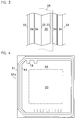
- Figures 3 and 4 show an upper surface 51a of lower semiconductor substrate 51.
- a plurality of P type base regions 33 are apposed to each other in N type base regions 30 in a latticed or striped pattern on a plane which includes upper surface 51a of lower semiconductor substrate 51.
- Two N type emitter regions 34 are formed in each P type base region 33 to extend along, adjacent to and in parallel to a longitudinal edge of P type base region 33 so that P type base region 33 and N type emitter regions 34 therein are incorporated together to define a minimum unit of a semiconductively active region referred to as a cell 20a.
- Gate electrodes 25 are formed on upper surface 51a of lower semiconductor substrate 51 in a striped pattern while laterally extending between and bridging adjacent P type base regions 33 to define cells 20a of semiconductively active region's minimum units in lower IGBT 1.
- N type emitter regions 34 are formed only on a central area of lower semiconductor substrate 51 and not on an outer periphery of lower semiconductor substrate 51 so that, as shown in Figure 4 , upper surface 1a of lower IGBT 1 comprises a cell-forming region 20 formed on the central area of lower IGBT 1 and a cell-free or non-cell region 44 annularly formed on the outer periphery of lower IGBT 1 for surrounding cell-forming region 20.
- P type base regions 33 may be formed into islands shape in N type base region 30.
- a gate bus line 43 is formed on upper surface 51a of lower semiconductor substrate 51 along a peripheral surface of lower semiconductor substrate 51 to electrically connect gate electrode 25 and separate electrode layer 18 formed on cell-free region 44 of lower IGBT 1.
- Both of separate electrode layer 18 and gate bus line 43 are made of conductive metallic material such as aluminum to cover an extension of striped gate electrodes 25 for electrical connection between separate electrode layer 18 or gate bus line 43 and gate electrode 25.
- separate electrode layer 18 and gate bus line 43 comprise a layered structure of polysilicon and aluminum on upper surface 51a of lower semiconductor substrate 51.
- Upper IGBT 2 has upper and lower surfaces 2a, 2b of their smaller areas than those of upper and lower surfaces 1a, 1b of lower IGBT 1.
- upper IGBT 2 comprises an upper semiconductor substrate 52 which also has a cell-forming region 20 on an upper surface 52a of upper semiconductor substrate 52, a gate insulation film formed on upper surface 52a of upper semiconductor substrate 52, a gate electrode formed on upper surface 52a of upper semiconductor substrate 52 through gate insulation film, an uppermost electrode layer (emitter electrode) 27 electrically connected to cells 20a, an intermediate insulation layer 26 for electrically isolating between gate electrode and uppermost electrode layer 27, and a collector electrode 14 formed on a bottom surface 52b of upper semiconductor substrate 52.
- an upper semiconductor substrate 52 which also has a cell-forming region 20 on an upper surface 52a of upper semiconductor substrate 52, a gate insulation film formed on upper surface 52a of upper semiconductor substrate 52, a gate electrode formed on upper surface 52a of upper semiconductor substrate 52 through gate insulation film, an uppermost electrode layer (emitter electrode) 27 electrically connected to cells 20
- upper IGBT 2 may comprises cell-forming region 20 only on the central area of upper semiconductor substrate 52, similarly to lower IGBT 1, and otherwise, cell-forming region 20 may be formed on the whole upper surface 52a of upper semiconductor substrate 52.
- Lower electrode layer 5 of lower IGBT 1 is electrically connected to N type emitter regions 34 and P type base regions 33. Also, lower electrode layer 5 extends to outside of cell-forming region 20 to cover a part of upper surface of cell-free region 44 in a plan view.
- Upper electrode layer 6 is formed on upper surface 5a of lower electrode layer 5 and extends to outside of cell-forming region 20 to cover a part of upper surface of cell-free region 44 in the plan view. In other words, cell-forming region 20 is located at a central area of lower semiconductor substrate 51 inside of cell-free region 44 in the plan view.
- Upper surfaces 5a and 6a of lower and upper electrode layers 5 and 6 are made of different materials from each other; lower electrode layer 5 has a connection layer 23 formed adjacent to upper electrode layer 6; connection layer 23 is powerfully adhesive to metallic material of wire 8; upper electrode layer 6 has a bonding layer 21 formed adjacent to solder layer 7 and an intermediate layer 22 formed between lower electrode layer 5 and bonding layer 21; and bonding layer 21 forms an upper surface 6a of upper electrode layer 6 which has a strongly adhesive property to a metallic material of solder layer 7.
- lower electrode layer 5 consists only of connection layer 23 made of a metallic material such as aluminum or silicon-containing aluminum powerfully adhesive to aluminum in wire 8.
- bonding layer 21 of upper electrode layer 6 is formed of a metallic material such as nickel superior in adhesion to solder layer 7, and intermediate layer 22 of upper electrode layer 6 is formed of for example titanium.
- lower electrode layer 5 may be formed by a layered structure of plural different metallic materials.
- bonding layer 21 of upper electrode layer 6 is made of nickel well wetting (compatible) to solder layer 7, but bonding layer 21 may be formed of another metallic material such as gold well wetting to solder layer 7.
- lower electrode layer 5 may be formed of another metallic material than aluminum as well.
- Intermediate layer 22 can be made of a suitably selected metallic material compatible to both bonding layer 21 and connection layer 23 of lower electrode layer 5.
- First and second protective films 9 and 29 are made of heat-resistible material such as polyimide film (PIF) or poly-benzothiazole (PBO), and first protective film 9 formed on lower IGBT 1 has openings 19 which expose bonding regions 15 of lower electrode layer 5 to the outside, and second protective film 29 formed on upper IGBT 2 has openings 39 which expose bonding regions 35 of uppermost electrode layer 27 to the outside.
- First and second protective layers 9 and 29 preserve lower and upper IGBTs 1 and 2 from entry of foreign matter such as ions therein.
- Uppermost electrode layer 27 on upper surface 2a of upper IGBT 2 is formed of metallic material powerfully adhesive to metallic material in wire 8 like lower electrode layer 5.
- each of bonding regions 15 of lower electrode layer 5 provides a wire connecting area (a wire bonding pad) for emitter electrode of lower IGBT 1 for connection for example to an outer element via wire 8.
- Upper surface 6a of upper electrode layer 6 has a bare area exposed to the outside through opening 19 of first protective film 9 to provide a soldering area (a die bonding pad) 16 for electrically connecting collector electrode 14 of upper IGBT 2 through solder layer 7.
- soldering area 16 of upper electrode layer 6 is formed into a nickel electrode surface of good solderability on which upper IGBT 2 is bonded via solder layer 7, whereas bonding region 15 is formed into an aluminum electrode surface superior in bonding of wire 8.
- upper surface 5a of lower electrode layer 5 can be made of one material firmly adhesive to wire 8
- upper surface 6a of upper electrode layer 6 can be made of another material of good solderability. Accordingly, solder layer 7 positively bonds between lower and upper IGBTs 1 and 2, and wire 8 can be strongly bonded on lower IGBT 1 to provide a reliable semiconductor device 10.
- the adhesive material used in the present invention includes bonding adhesives, more preferably electrically conductive adhesive agent such as soldering material, brazing material and silver paste.
- Soldering material basically includes lead-free solder such as tin, silver, copper or aluminum, however, typical and other well-known solders including tin and lead may also be used.
- Wire 8 may include well-known wiring made of gold, aluminum or silicon-containing aluminum.
- lower IGBT 1 is prepared which has cell-forming region 20 of plural cells 20a in the central area on upper surface 1a
- upper IGBT 2 is prepared which has also cell-forming region on upper surface 2a.
- lower IGBT 1 has cell-forming region 20 formed in the central area on upper surface 51a of lower semiconductor substrate 51, and cell-free region 44 annularly formed for surrounding cell-forming region 20.
- further description is omitted herein because a method for making a semiconductor element such as lower and upper IGBTs 1 and 2 is well-known.
- lower electrode layer 5 is formed of aluminum on upper surface 51a of lower semiconductor substrate 51 utilizing a well-known technique of for example vapor deposition such as chemical or physical vapor deposition (CVD, PVD) or plating. Then, an etching mask (not shown) is covered on upper surface 5a of lower electrode layer 5, and etching solution, which preferably contains phosphoric acid capable of dissolving aluminum, is poured in openings formed in etching mask to remove unnecessary portions of lower electrode layer 5 and thereby form cutouts 37 between lower electrode layer 5 and separate electrode layer 18. Lower electrode layer 5 extends beyond outer periphery of cell-forming region 20 to cover a part of upper surface of cell-free region 44 in the plan view.
- CVD chemical or physical vapor deposition
- PVD physical vapor deposition
- intermediate layer 22 of titanium and bonding layer 21 of nickel are formed in order on upper surface 5a of lower electrode layer 5 to complete upper electrode layer 6 in a similar manner to that for making up lower electrode layer 5.
- an etching mask is formed on upper surface 6a of upper electrode layer 6, and metal etching solution, which preferably contains hydrochloric acid capable of simultaneously dissolving titanium and nickel, is poured in openings formed in etching mask to remove unnecessary portions of upper electrode layer 6 as shown in Figure 7 . Titanium and nickel can be in turn removed with different etching solutions supplied into openings.
- this etching process concurrently serves to cut off a portion of upper electrode layer 6 outside of cell-forming region 20 and over a part of cell-free region 44, and thereby form notches 36 in upper electrode layer 6 to expose to the outside bonding regions 15 on upper surface 5a of lower electrode layer 5 through notches 36. Accordingly, upper electrode 6 extends beyond cell-forming region 20 to a part of cell-free region 44 in the plan view to form bonding regions 15 on lower electrode layer 5 outside of cell-forming region 20 on lower semiconductor substrate 51.
- lower electrode layer 5 may also disadvantageously be etched together with upper electrode layer 6, however, electrode layer 5 can positively prevent etching of cell-forming region 20 to avoid degradation of electric property in the semiconductor device because etching process cuts off a portion of upper electrode layer 6 outside of cell-forming region 20.
- lower electrode layer 5 serves to electrically connect P type base regions 33 and N type emitter regions 34 in multiple cells 20a, and therefore, etching of lower electrode layer 5 formed on cell-forming region 20 may cause undesirable damage to electric property of lower IGBT 1.
- upper electrode layer 6 extends to cell-free region 44 outside of cell-forming region 20 in lower IGBT 1 to provide bonding region 15, and etching of upper electrode layer 6 over cell-free region 44, if any, hardly causes any damage to cell-forming region 20 and electric property of lower IGBT 1 to provide a highly reliable semiconductor device of stable electric property.
- first protective film 9 is formed to seal each appropriate portion of upper electrode layer 6, separate electrode layer 18 and lower electrode layer 5 while at the same time providing openings 19 to expose to the outside two bonding pad areas on bonding region 15 and separate electrode layer 18 and also a pad area on soldering area 16.
- upper IGBT 2 is secured on soldering area 16 over lower IGBT 1 through solder layer 7 in opening 19.
- Upper IGBT 2 has preformed uppermost electrode layer 27, second protective film 29 and collector electrode 14.
- First protective film 9 is formed in an annular shape as shown in Figure 9 to settle upper IGBT 2 in position because solder layer 7 for supporting upper IGBT 2 can properly be secured on soldering area 16 surrounded by first protective film 9.
- first protective film 9 serves to dam molten solder layer 7 and prevent effusion thereof from soldering area 16 encompassed by first protective film 9. This ensures relatively thicker solder layer 7 on soldering area 16, and heat produced during operation of the semiconductor device 10 can be radiated to the outside through thicker solder layer 7.
- Collector electrode 13 formed on bottom surface 51b of lower semiconductor substrate 51 is secured on an upper surface of a support plate 45 via solder. Also, each one end of wires 8 shown in Figure 1 is connected to outer elements or outer leads and each the other end of wires 8 is connected to bonding regions 15 and 35 and separate electrode layer 18 of lower and upper IGBTs 1 and 2 to finish the semiconductor device 10.
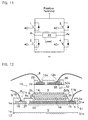
- FIG 10 illustrates a further embodiment of a semiconductor device 50 according to the present invention as a single unit of H-type bridge circuit of Figure 11 formed into a configuration of the semiconductor device 10 shown in Figure 1 .
- H-type bridge circuit comprises first and second lower IGBTs 1 and 3 of high-voltage side and first and second upper IGBTs 2 and 4 of low-voltage side.
- a first stack of first lower and upper IGBTs 1 and 2 and a second stack of second lower and upper IGBTs 3 and 4 are mounted on a support plate 45 formed of heat radiating metallic material such as copper or aluminum.
- Semiconductor device 50 further comprises a control device 40 for controlling switching operation of lower and upper IGBTs 1 to 4, a plurality of outer leads 42 disposed around support plate 45, and wires 8 for electrically connecting surface electrodes of control device 40, bonding regions (emitter electrodes) 15 and 35 and separate electrodes (gate electrodes) 18 of lower and upper IGBTs 1 and 2. As shown in Figure 10 , control device 40 is secured on support plate 45 between first and second stacks.
- An electric load 41 is connected between a junction A 1 of lower electrode layer (an emitter electrode) 5 of first lower IGBT 1 and collector electrode 14 of first upper IGBT 2 and a junction A 2 of lower electrode layer (an emitter electrode) of second lower IGBT 3 and collector electrode of second upper IGBT 4, and by way of example, electric load 41 comprises a cold cathode fluorescent discharge tube driven by alternating current.
- electric load 41 comprises a cold cathode fluorescent discharge tube driven by alternating current.
- a whole of semiconductor device 50 is encapsulated by a plastic encapsulant 48 from which outer leads 42 are derived to the outside.
- control device 40 is operated to alternately turn on and off a first pair of first lower IGBT 1 and second upper IGBT 4 and a second pair of first upper IGBT 2 and second lower IGBT 3 to produce alternate current flowing through load 41 or cold cathode fluorescent discharge tube in the bilaterally adverse directions between junctions A 1 and A 2 so that discharge tube can be lighted up.
- cold cathode fluorescent discharge tube can be lighted by switching operation of first and second pairs of first lower, second upper, first upper and second lower IGBTs 1 to 4 utilizing a power source of DC voltage.
- Semiconductor device 50 shown in Figure 10 can have its reduced occupation space with the improved integration degree.
- upper IGBTs 2 and 4 can be firmly secured respectively on lower IGBTs 1 and 3 via solder layer 7, and wires 8 can be strongly connected on each of IGBTs 1 to 4 to provide the reliable semiconductor device.
- Embodiments of the present invention may be varied in various ways without limitation to the foregoing embodiments.
- other semiconductor devices may be used such as other type of bipolar transistors, field-effect transistors, thyristors or triacs.
- upper electrode layer 6 may be formed on upper surface 5a of lower electrode layer 5 which is protected by first protective film 9 to preferably prevent etching of lower electrode layer 5 when unnecessary portions of upper electrode layer 6 over first protective film 9 are removed by etching.
- the present invention can preferably be applied to semiconductor devices which have a plurality of piled semiconducting elements, especially those for configuring an H-type bridge circuit (full bridge circuit) for use in driving a cold cathode fluorescent discharge tube.
Landscapes
- Electrodes Of Semiconductors (AREA)
- Wire Bonding (AREA)
Abstract
Description
- This invention relates to a semiconductor device, in particular of the type having a plurality of semiconducting elements laid one on top of another for the small-sized semiconductor device.
- The following
Patent Document 1 discloses a known semiconductor device which comprises a metallic support plate, first and second transistors piled up in turn on the support plate, third and fourth transistors piled up in turn on the support plate, and a control circuit (control IC) mounted on the support plate and between the first and second transistors and between the third and fourth transistors to cause the first, second, third and fourth transistors to form an H-type bridge circuit. InPatent Document 1, first and second transistors are stacked, and third and fourth transistors are stacked to reduce occupation space of the support plate and increase the integration degree of the device. - Also, in the semiconductor device of
Patent Document 1, each lower electrode formed on the bottom surface of second and fourth transistors is secured by solder on each upper electrode formed on the top surface of first and third transistors, and upper electrodes of first and third transistors are electrically connected via wires to an upper electrode of the control circuit and a plurality of outer leads disposed around the support plate. The direct electric connections by solder between first and second transistors and between third and fourth transistors serve to advantageously shorten flow paths of electric current while preventing noise and power loss which may occur with an elongated flow path and also simplifying wiring connections. - [Patent Document 1]
WO 2005/018001 - In the above semiconductor device, upper electrodes of first and third transistors located on the bottom side are made of any metallic material suitable for bonding by solder to lower electrodes of second and fourth transistors or for bonding to wiring. Electrodes formed of metallic material such as nickel or copper excellent in good soldering property are inferior in bonding to wiring formed of metallic material such as aluminum or gold. Also, electrodes formed of metallic material such as aluminum indicating a high adhesive strength to wiring, are inferior in bonding or wetting to solder consisting of metallic material such as lead or tin. For that reason, the semiconductor device shown in
Patent Document 1 cannot have simultaneous high adhesive strengths to both solder and wiring.
Accordingly, an object of the present invention is to provide a semiconductor device superior in adhesive strengths to both solder and wiring, and a manufacture of the semiconductor device. - The semiconductor device according to the present invention, comprises a lower semiconducting element (1), a lower electrode layer (5) formed on an upper surface (1a) of lower semiconducting element (1), an upper electrode layer (6) formed on an upper surface (5a) of lower electrode layer (5), an upper semiconducting element (2) secured on an upper surface (6a) of upper electrode layer (6), and an adhesive layer (7) for bonding upper electrode layer (6) and upper semiconducting element (2). Upper surfaces (5a, 6a) of lower and upper electrode layers (5, 6) are formed of different materials from each other. Upper surface (5a) of lower electrode layer (5) have a bonding region (15) exposed to outside of upper electrode layer (6) to attach an end of a lead wire (8) on bonding region (15).
- The method for producing a semiconductor device according to the present invention, comprises the steps of forming a lower electrode layer (5) on an upper surface (1a) of a lower semiconducting element (1), forming an upper electrode layer (6) on an upper surface (5a) of lower electrode layer (5), the upper electrode layer (6) having an upper surface (6a) formed of a material different from that of upper surface (5a) of lower electrode layer (5), forming a notch (36) in upper electrode layer (6) to partly define on upper surface (5a) of lower electrode layer (5) a bonding region (15) exposed to the outside through notch (35), securing through an adhesive layer (7) an upper semiconducting element (2) on upper surface (6a) of upper electrode layer (6), and bonding an end of a lead wire (8) on bonding region (15).
- As upper surfaces (5a, 6a) of lower and upper electrode layers (5, 6) provided between lower and upper semiconducting elements (1, 2) can be made of different materials, upper surface (6a) of upper electrode layer (6) can be made of a material superior in soldering property, and upper surface (5a) of lower electrode (5) can be made of another material having a high bonding or adhesive strength to lead wire (8). Accordingly, lower and upper semiconducting elements (1, 2) can be preferably bonded through adhesive layer (7) such as solder or the like, and lead wire (8) can be firmly joined to lower semiconducting element (1) to provide a reliable semiconductor device.
- In accordance with the present invention, a semiconductor device can be materialized which has high bonding or adhesive strengths of both soldering between upper and lower semiconducting elements and joining of wiring to semiconductor elements.
-
- [
Figure 1 ] A cross section showing an embodiment of a semiconductor device according to the present invention; - [
Figure 2 ] A partly enlarged view ofFigure 1 ; - [
Figure 3 ] A partly enlarged view of a lower semiconductor substrate inFigure 1 ; - [
Figure 4 ] A plan view of the lower semiconductor substrate inFigure 1 ; - [
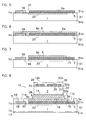
Figure 5 ] A cross section of a lower electrode layer formed on an upper surface of the lower semiconductor substrate; - [
Figure 6 ] A cross section of an upper electrode layer formed on an upper surface of the lower electrode layer inFigure 5 ; - [
Figure 7 ] A cross section of the etched upper electrode layer inFigure 6 ; - [
Figure 8 ] A cross section of an upper IGBT on the upper electrode layer inFigure 6 ; - [
Figure 9 ] A plan view showing a first protective film coated on a lower semiconductor substrate inFigure 7 ; - [
Figure 10 ] A plan view showing an embodiment of the semiconductor device inFigure 1 ; - [
Figure 11 ] An electric circuit diagram ofFigure 10 ; and - [
Figure 12 ] A cross section showing a varied embodiment of the semiconductor device inFigure 1 . - 1·· A lower semiconducting element (A lower IGBT), 1a, 2a, 5a, 6a·· Upper surfaces, 2·· An upper semiconducting element (An upper IGBT), 5·· A lower electrode layer, 6·· An upper electrode layer, 7·· A solder layer, 8·· Lead wires (Wiring); 9·· A protective layer, 15·· A bonding region, 19·· Openings, 20·· Cell- forming regions, 20a·· Cells, 21·· A bonding layer, 23·· A connection layer, 36·· A notch, 40·· A control device.
- Embodiments of the semiconductor device and its manufacture according to the present invention are described hereinafter with reference to
Figures 1 to 12 .
As shown inFigure 1 , the semiconductor device of this embodiment comprises a lower IGBT 1 (Insulated Gate Bipolar Transistor) as a lower semiconducting element, alower electrode layer 5 formed on anupper surface 1a oflower IGBT 1, a separate electrode layer (a gate pad) 18 formed onupper surface 1a oflower IGBT 1 away fromlower electrode layer 5, anupper electrode layer 6 formed on anupper surface 5a oflower electrode layer 5, anupper IGBT 2 as an upper semiconducting element secured onupper surface 6a ofupper electrode layer 6 by asolder layer 7 as an adhesive layer, anuppermost electrode layer 27 formed on anupper surface 2a ofupper IGBT 2, a first nonconductiveprotective film 9 which seals each portion ofupper electrode layer 6,separate electrode layer 18,lower electrode layer 5 and the like, and a second nonconductiveprotective film 29 which seals a portion of anuppermost electrode layer 27 and the like.Lower electrode layer 5 has abonding region 15 exposed to the outside through anotch 36 formed inupper electrode layer 6 andopenings 19 formed in first nonconductiveprotective film 9. One end of awire 8 as a lead wire is connected by wire-bonding toflat bonding region 15. - As shown in
Figure 2 ,lower IGBT 1 comprises alower semiconductor substrate 51 formed of for example silicon monocrystal, agate insulation film 24 formed of for example silicon dioxide on anupper surface 51a oflower semiconductor substrate 51, a gate (control)electrode 25 formed of for example polysilicon on anupper surface 51a oflower semiconductor substrate 51 throughgate insulation film 24, anintermediate insulation layer 26 which electrically isolates betweengate electrode 25 andlower electrode layer 5, and collector (bottom)electrode 13 formed by layering aluminum and nickel on abottom surface 51b oflower semiconductor substrate 51. -
Lower semiconductor substrate 51 comprises acollector region 31 of P+ type semiconductor region for formingbottom surface 51b oflower semiconductor substrate 51, N-type buffer region 32 formed oncollector region 31, Ntype base region 30 formed on N-type buffer region 32, Ptype base region 33 formed within Ntype base region 30 at the same level asupper surface 51a oflower semiconductor substrate 51, and an Ntype emitter region 34 formed within Ptype base region 33 at the same level asupper surface 51a oflower semiconductor substrate 51.Gate electrodes 25 are formed throughgate insulation film 24 on Ptype base regions 33 formed between Ntype emitter region 34 and Ntype base region 30 to define a well-known channel region between Ntype base region 30 andemitter region 34 in Ptype base region 33 adjacent togate insulation film 24. As shown inFigure 2 ,openings 26a are formed inintermediate insulation layer 26 which electrically isolates betweengate electrode 25 andlower electrode layer 5, andlower electrode layer 5 is electrically connected to Ntype emitter region 34 and Ptype base region 33 throughopenings 26a to form emitter electrodes. -
Figures 3 and 4 show anupper surface 51a oflower semiconductor substrate 51. As shown inFigure 3 , a plurality of Ptype base regions 33 are apposed to each other in Ntype base regions 30 in a latticed or striped pattern on a plane which includesupper surface 51a oflower semiconductor substrate 51. Two Ntype emitter regions 34 are formed in each Ptype base region 33 to extend along, adjacent to and in parallel to a longitudinal edge of Ptype base region 33 so that Ptype base region 33 and Ntype emitter regions 34 therein are incorporated together to define a minimum unit of a semiconductively active region referred to as acell 20a.Gate electrodes 25 are formed onupper surface 51a oflower semiconductor substrate 51 in a striped pattern while laterally extending between and bridging adjacent Ptype base regions 33 to definecells 20a of semiconductively active region's minimum units inlower IGBT 1. In the semiconductor device of this embodiment, Ntype emitter regions 34 are formed only on a central area oflower semiconductor substrate 51 and not on an outer periphery oflower semiconductor substrate 51 so that, as shown inFigure 4 ,upper surface 1a oflower IGBT 1 comprises a cell-formingregion 20 formed on the central area oflower IGBT 1 and a cell-free ornon-cell region 44 annularly formed on the outer periphery oflower IGBT 1 for surrounding cell-formingregion 20. Alternatively, Ptype base regions 33 may be formed into islands shape in Ntype base region 30. - Also, a
gate bus line 43 is formed onupper surface 51a oflower semiconductor substrate 51 along a peripheral surface oflower semiconductor substrate 51 to electrically connectgate electrode 25 andseparate electrode layer 18 formed on cell-free region 44 oflower IGBT 1. Both ofseparate electrode layer 18 andgate bus line 43 are made of conductive metallic material such as aluminum to cover an extension ofstriped gate electrodes 25 for electrical connection betweenseparate electrode layer 18 orgate bus line 43 andgate electrode 25. To this end,separate electrode layer 18 andgate bus line 43 comprise a layered structure of polysilicon and aluminum onupper surface 51a oflower semiconductor substrate 51. -
Upper IGBT 2 has upper andlower surfaces lower surfaces lower IGBT 1. Although not shown in detail in the drawings, but,upper IGBT 2 comprises anupper semiconductor substrate 52 which also has a cell-formingregion 20 on anupper surface 52a ofupper semiconductor substrate 52, a gate insulation film formed onupper surface 52a ofupper semiconductor substrate 52, a gate electrode formed onupper surface 52a ofupper semiconductor substrate 52 through gate insulation film, an uppermost electrode layer (emitter electrode) 27 electrically connected tocells 20a, anintermediate insulation layer 26 for electrically isolating between gate electrode anduppermost electrode layer 27, and acollector electrode 14 formed on abottom surface 52b ofupper semiconductor substrate 52. It should be noted that, although a same reference symbol "20" is applied for the only purpose of illustration to cell-forming region on anupper surface 52a ofupper semiconductor substrate 52 and cell-forming region on the central area oflower IGBT 1, these cell-forming regions are completely different from each other. However,upper IGBT 2 may comprises cell-formingregion 20 only on the central area ofupper semiconductor substrate 52, similarly tolower IGBT 1, and otherwise, cell-formingregion 20 may be formed on the wholeupper surface 52a ofupper semiconductor substrate 52. -
Lower electrode layer 5 oflower IGBT 1 is electrically connected to Ntype emitter regions 34 and Ptype base regions 33. Also,lower electrode layer 5 extends to outside of cell-formingregion 20 to cover a part of upper surface of cell-free region 44 in a plan view.Upper electrode layer 6 is formed onupper surface 5a oflower electrode layer 5 and extends to outside of cell-formingregion 20 to cover a part of upper surface of cell-free region 44 in the plan view. In other words, cell-formingregion 20 is located at a central area oflower semiconductor substrate 51 inside of cell-free region 44 in the plan view. -
Upper surfaces lower electrode layer 5 has aconnection layer 23 formed adjacent toupper electrode layer 6;connection layer 23 is powerfully adhesive to metallic material ofwire 8;upper electrode layer 6 has abonding layer 21 formed adjacent tosolder layer 7 and anintermediate layer 22 formed betweenlower electrode layer 5 andbonding layer 21; andbonding layer 21 forms anupper surface 6a ofupper electrode layer 6 which has a strongly adhesive property to a metallic material ofsolder layer 7. As illustrated inFigure 2 ,lower electrode layer 5 consists only ofconnection layer 23 made of a metallic material such as aluminum or silicon-containing aluminum powerfully adhesive to aluminum inwire 8. On the contrary,bonding layer 21 ofupper electrode layer 6 is formed of a metallic material such as nickel superior in adhesion tosolder layer 7, andintermediate layer 22 ofupper electrode layer 6 is formed of for example titanium. Likewise,lower electrode layer 5 may be formed by a layered structure of plural different metallic materials. - In this embodiment,
bonding layer 21 ofupper electrode layer 6 is made of nickel well wetting (compatible) tosolder layer 7, butbonding layer 21 may be formed of another metallic material such as gold well wetting tosolder layer 7. Also,lower electrode layer 5 may be formed of another metallic material than aluminum as well.Intermediate layer 22 can be made of a suitably selected metallic material compatible to bothbonding layer 21 andconnection layer 23 oflower electrode layer 5. - First and second
protective films protective film 9 formed onlower IGBT 1 hasopenings 19 which exposebonding regions 15 oflower electrode layer 5 to the outside, and secondprotective film 29 formed onupper IGBT 2 hasopenings 39 which exposebonding regions 35 ofuppermost electrode layer 27 to the outside. First and secondprotective layers upper IGBTs Uppermost electrode layer 27 onupper surface 2a ofupper IGBT 2 is formed of metallic material powerfully adhesive to metallic material inwire 8 likelower electrode layer 5. - As shown in
Figure 1 , each ofbonding regions 15 oflower electrode layer 5 provides a wire connecting area (a wire bonding pad) for emitter electrode oflower IGBT 1 for connection for example to an outer element viawire 8.Upper surface 6a ofupper electrode layer 6 has a bare area exposed to the outside through opening 19 of firstprotective film 9 to provide a soldering area (a die bonding pad) 16 for electrically connectingcollector electrode 14 ofupper IGBT 2 throughsolder layer 7. In other words, solderingarea 16 ofupper electrode layer 6 is formed into a nickel electrode surface of good solderability on whichupper IGBT 2 is bonded viasolder layer 7, whereasbonding region 15 is formed into an aluminum electrode surface superior in bonding ofwire 8. As the present invention can allow different metallic materials to be formed intoupper surfaces upper IGBTs upper surface 5a oflower electrode layer 5 can be made of one material firmly adhesive towire 8, andupper surface 6a ofupper electrode layer 6 can be made of another material of good solderability. Accordingly,solder layer 7 positively bonds between lower andupper IGBTs wire 8 can be strongly bonded onlower IGBT 1 to provide areliable semiconductor device 10. The adhesive material used in the present invention includes bonding adhesives, more preferably electrically conductive adhesive agent such as soldering material, brazing material and silver paste. Soldering material basically includes lead-free solder such as tin, silver, copper or aluminum, however, typical and other well-known solders including tin and lead may also be used.Wire 8 may include well-known wiring made of gold, aluminum or silicon-containing aluminum. - In making the
semiconductor device 10 shown inFigure 1 ,lower IGBT 1 is prepared which has cell-formingregion 20 ofplural cells 20a in the central area onupper surface 1a, and likewise,upper IGBT 2 is prepared which has also cell-forming region onupper surface 2a. As shown inFigure 3 ,lower IGBT 1 has cell-formingregion 20 formed in the central area onupper surface 51a oflower semiconductor substrate 51, and cell-free region 44 annularly formed for surrounding cell-formingregion 20. However, further description is omitted herein because a method for making a semiconductor element such as lower andupper IGBTs - As shown in
Figure 5 ,lower electrode layer 5 is formed of aluminum onupper surface 51a oflower semiconductor substrate 51 utilizing a well-known technique of for example vapor deposition such as chemical or physical vapor deposition (CVD, PVD) or plating. Then, an etching mask (not shown) is covered onupper surface 5a oflower electrode layer 5, and etching solution, which preferably contains phosphoric acid capable of dissolving aluminum, is poured in openings formed in etching mask to remove unnecessary portions oflower electrode layer 5 and thereby formcutouts 37 betweenlower electrode layer 5 andseparate electrode layer 18.Lower electrode layer 5 extends beyond outer periphery of cell-formingregion 20 to cover a part of upper surface of cell-free region 44 in the plan view. - Subsequently, as shown in
Figure 6 ,intermediate layer 22 of titanium andbonding layer 21 of nickel are formed in order onupper surface 5a oflower electrode layer 5 to completeupper electrode layer 6 in a similar manner to that for making uplower electrode layer 5. This ensures that lower and upper electrode layers 5 and 6 can be layered onupper surface 1a oflower IGBT 1. Then, an etching mask is formed onupper surface 6a ofupper electrode layer 6, and metal etching solution, which preferably contains hydrochloric acid capable of simultaneously dissolving titanium and nickel, is poured in openings formed in etching mask to remove unnecessary portions ofupper electrode layer 6 as shown inFigure 7 . Titanium and nickel can be in turn removed with different etching solutions supplied into openings. Also, this etching process concurrently serves to cut off a portion ofupper electrode layer 6 outside of cell-formingregion 20 and over a part of cell-free region 44, and thereby formnotches 36 inupper electrode layer 6 to expose to theoutside bonding regions 15 onupper surface 5a oflower electrode layer 5 throughnotches 36. Accordingly,upper electrode 6 extends beyond cell-formingregion 20 to a part of cell-free region 44 in the plan view to formbonding regions 15 onlower electrode layer 5 outside of cell-formingregion 20 onlower semiconductor substrate 51. - During etching process of
upper electrode layer 6 with etching solution,lower electrode layer 5 may also disadvantageously be etched together withupper electrode layer 6, however,electrode layer 5 can positively prevent etching of cell-formingregion 20 to avoid degradation of electric property in the semiconductor device because etching process cuts off a portion ofupper electrode layer 6 outside of cell-formingregion 20. In other words,lower electrode layer 5 serves to electrically connect Ptype base regions 33 and Ntype emitter regions 34 inmultiple cells 20a, and therefore, etching oflower electrode layer 5 formed on cell-formingregion 20 may cause undesirable damage to electric property oflower IGBT 1. To avoid such damage,upper electrode layer 6 extends to cell-free region 44 outside of cell-formingregion 20 inlower IGBT 1 to providebonding region 15, and etching ofupper electrode layer 6 over cell-free region 44, if any, hardly causes any damage to cell-formingregion 20 and electric property oflower IGBT 1 to provide a highly reliable semiconductor device of stable electric property. - After that, first
protective film 9 is formed to seal each appropriate portion ofupper electrode layer 6,separate electrode layer 18 andlower electrode layer 5 while at the sametime providing openings 19 to expose to the outside two bonding pad areas onbonding region 15 andseparate electrode layer 18 and also a pad area onsoldering area 16. As shown inFigure 8 ,upper IGBT 2 is secured onsoldering area 16 overlower IGBT 1 throughsolder layer 7 inopening 19.Upper IGBT 2 has preformeduppermost electrode layer 27, secondprotective film 29 andcollector electrode 14. Firstprotective film 9 is formed in an annular shape as shown inFigure 9 to settleupper IGBT 2 in position becausesolder layer 7 for supportingupper IGBT 2 can properly be secured onsoldering area 16 surrounded by firstprotective film 9. In this way,upper IGBT 2 can be soldered in position oflower IGBT 1 with accuracy as shown inFigure 1 , and firstprotective film 9 serves to dammolten solder layer 7 and prevent effusion thereof from solderingarea 16 encompassed by firstprotective film 9. This ensures relativelythicker solder layer 7 onsoldering area 16, and heat produced during operation of thesemiconductor device 10 can be radiated to the outside throughthicker solder layer 7. -
Collector electrode 13 formed onbottom surface 51b oflower semiconductor substrate 51 is secured on an upper surface of asupport plate 45 via solder. Also, each one end ofwires 8 shown inFigure 1 is connected to outer elements or outer leads and each the other end ofwires 8 is connected tobonding regions separate electrode layer 18 of lower andupper IGBTs semiconductor device 10. -
Figure 10 illustrates a further embodiment of asemiconductor device 50 according to the present invention as a single unit of H-type bridge circuit ofFigure 11 formed into a configuration of thesemiconductor device 10 shown inFigure 1 . H-type bridge circuit comprises first and secondlower IGBTs upper IGBTs upper IGBTs upper IGBTs support plate 45 formed of heat radiating metallic material such as copper or aluminum.Semiconductor device 50 further comprises acontrol device 40 for controlling switching operation of lower andupper IGBTs 1 to 4, a plurality ofouter leads 42 disposed aroundsupport plate 45, andwires 8 for electrically connecting surface electrodes ofcontrol device 40, bonding regions (emitter electrodes) 15 and 35 and separate electrodes (gate electrodes) 18 of lower andupper IGBTs Figure 10 ,control device 40 is secured onsupport plate 45 between first and second stacks. Anelectric load 41 is connected between a junction A1 of lower electrode layer (an emitter electrode) 5 of firstlower IGBT 1 andcollector electrode 14 of firstupper IGBT 2 and a junction A2 of lower electrode layer (an emitter electrode) of secondlower IGBT 3 and collector electrode of secondupper IGBT 4, and by way of example,electric load 41 comprises a cold cathode fluorescent discharge tube driven by alternating current. Typically, a whole ofsemiconductor device 50 is encapsulated by a plastic encapsulant 48 from which outer leads 42 are derived to the outside. - In operation of H-type bridge circuit,
control device 40 is operated to alternately turn on and off a first pair of firstlower IGBT 1 and secondupper IGBT 4 and a second pair of firstupper IGBT 2 and secondlower IGBT 3 to produce alternate current flowing throughload 41 or cold cathode fluorescent discharge tube in the bilaterally adverse directions between junctions A1 and A2 so that discharge tube can be lighted up. In this way, cold cathode fluorescent discharge tube can be lighted by switching operation of first and second pairs of first lower, second upper, first upper and secondlower IGBTs 1 to 4 utilizing a power source of DC voltage.Semiconductor device 50 shown inFigure 10 can have its reduced occupation space with the improved integration degree. At the same time,upper IGBTs lower IGBTs solder layer 7, andwires 8 can be strongly connected on each ofIGBTs 1 to 4 to provide the reliable semiconductor device. - Embodiments of the present invention may be varied in various ways without limitation to the foregoing embodiments. For example, in lieu of each IGBTs 1 to 4, other semiconductor devices may be used such as other type of bipolar transistors, field-effect transistors, thyristors or triacs. Moreover, as shown in
Figure 12 , after coatinglower electrode layer 5 with firstprotective film 9,upper electrode layer 6 may be formed onupper surface 5a oflower electrode layer 5 which is protected by firstprotective film 9 to preferably prevent etching oflower electrode layer 5 when unnecessary portions ofupper electrode layer 6 over firstprotective film 9 are removed by etching. - The present invention can preferably be applied to semiconductor devices which have a plurality of piled semiconducting elements, especially those for configuring an H-type bridge circuit (full bridge circuit) for use in driving a cold cathode fluorescent discharge tube.
Claims (5)
- A semiconductor device comprising a lower semiconducting element (1), a lower electrode layer (5) formed on an upper surface (1a) of said lower semiconducting element (1), an upper electrode layer (6) formed on an upper surface (5a) of said lower electrode layer (5), an upper semiconducting element (2) secured on an upper surface (6a) of said upper electrode layer (6), and an adhesive layer (7) for bonding said upper electrode layer (6) and upper semiconducting element (2),
the upper surfaces (5a, 6a) of said lower and upper electrode layers (5, 6) being formed of different materials from each other, and
the upper surface (5a) of said lower electrode layer (5) having a bonding region (15) exposed to outside of the upper electrode layer (6) to attach an end of a lead wire (8) on said bonding region (15). - The semiconductor device of claim 1, wherein the upper surface (5a) of said lower electrode layer (5) is formed of a metallic material which has a higher adhesive property to the metallic lead wire (8) than that of the upper surface of said upper electrode layer (6), and
the upper surface of said upper electrode layer (6) is formed of a metallic material which has a higher adhesive property to said adhesive layer (7) than that of the upper surface (5a) of said lower electrode layer (5). - The semiconductor device of claim 1, wherein the upper surface (1a) of said lower semiconducting element (1) has a cell-forming region (20) which has a plurality of cells (20a) functionable as semiconductively active regions, and a cell-free region (44) which has no cell,
the cell-forming region (20) is arranged on a central area of said lower semiconducting element (1),
the cell-free region (44) is annularly arranged on an outer periphery of said lower semiconducting element (1) to surround the cell-forming region (20) by the cell-free region (44),
said upper electrode layer (6) extends beyond the cell-forming region (20) into the outer periphery of said lower semiconducting element (1). - A method for producing a semiconductor device, comprising the steps of:forming a lower electrode layer (5) on an upper surface (1a) of a lower semiconducting element (1),forming an upper electrode layer (6) on an upper surface (5a) of said lower electrode layer (5), the upper electrode layer (6) having an upper surface (6a) formed of a material different from that of the upper surface (5a) of said lower electrode layer (5),forming a notch (36) in said upper electrode layer (6) to partly define on the upper surface (5a) of said lower electrode layer (5) a bonding region (15) exposed to the outside through said notch (36),securing an upper semiconducting element (2) on the upper surface (6a) of said upper electrode layer (6) through an adhesive layer (7), andbonding an end of a lead wire (8) on said bonding region (15).
- The method of claim 4, further comprising: providing on the upper surface (1a) of a lower semiconducting element (1) a cell-forming region (20) which has a plurality of cells (20a) functionable as semiconductively active regions and a cell-free region (44) which has no cell,
wherein the defining of said bonding region (15) on the upper surface (5a) of said lower electrode layer (5) comprises removing by etching a part of said upper electrode layer (6) outside of the cell-forming region (20).
Applications Claiming Priority (2)
| Application Number | Priority Date | Filing Date | Title |
|---|---|---|---|
| JP2005198447A JP2007019215A (en) | 2005-07-07 | 2005-07-07 | Semiconductor device and manufacturing method thereof |
| PCT/JP2006/305702 WO2007007445A1 (en) | 2005-07-07 | 2006-03-22 | Semiconductor device and method for manufacturing same |
Publications (3)
| Publication Number | Publication Date |
|---|---|
| EP1906452A1 true EP1906452A1 (en) | 2008-04-02 |
| EP1906452A4 EP1906452A4 (en) | 2008-07-09 |
| EP1906452B1 EP1906452B1 (en) | 2012-08-29 |
Family
ID=37636845
Family Applications (1)
| Application Number | Title | Priority Date | Filing Date |
|---|---|---|---|
| EP06729669A Expired - Lifetime EP1906452B1 (en) | 2005-07-07 | 2006-03-22 | Semiconductor device |
Country Status (5)
| Country | Link |
|---|---|
| US (1) | US7847316B2 (en) |
| EP (1) | EP1906452B1 (en) |
| JP (1) | JP2007019215A (en) |
| CN (1) | CN101040386B (en) |
| WO (1) | WO2007007445A1 (en) |
Cited By (2)
| Publication number | Priority date | Publication date | Assignee | Title |
|---|---|---|---|---|
| WO2016094718A1 (en) | 2014-12-10 | 2016-06-16 | Texas Instruments Incorporated | Power field-effect transistor (fet), pre-driver, controller, and sense resistor integration |
| EP2272075B1 (en) * | 2007-05-16 | 2021-03-10 | QUALCOMM Incorporated | Semiconductor die stack |
Families Citing this family (9)
| Publication number | Priority date | Publication date | Assignee | Title |
|---|---|---|---|---|
| JP2007019215A (en) | 2005-07-07 | 2007-01-25 | Sanken Electric Co Ltd | Semiconductor device and manufacturing method thereof |
| JP2008244388A (en) * | 2007-03-29 | 2008-10-09 | Nec Electronics Corp | Semiconductor device |
| EP2330793B1 (en) | 2009-12-02 | 2016-06-29 | Chalk Media Service Corp. | System and Method for Centrally Distributing Mobile Content |
| US8866302B2 (en) * | 2011-01-25 | 2014-10-21 | Infineon Technologies Ag | Device including two semiconductor chips and manufacturing thereof |
| KR101420536B1 (en) * | 2012-12-14 | 2014-07-17 | 삼성전기주식회사 | Power module package |
| US9455253B2 (en) * | 2014-07-23 | 2016-09-27 | Stmicroelectronics (Tours) Sas | Bidirectional switch |
| CN104791734B (en) * | 2015-04-21 | 2018-02-23 | 乐健科技(珠海)有限公司 | The manufacture method of radiator with embedded lines, the manufacture method of LED module |
| JP7059677B2 (en) * | 2018-02-16 | 2022-04-26 | 富士電機株式会社 | Stacked integrated circuit |
| CN110993516B (en) * | 2019-12-13 | 2021-06-25 | 上海贝岭股份有限公司 | Self-clamping IGBT device and manufacturing method thereof |
Family Cites Families (13)
| Publication number | Priority date | Publication date | Assignee | Title |
|---|---|---|---|---|
| JPS61239656A (en) * | 1985-04-16 | 1986-10-24 | Citizen Watch Co Ltd | Semiconductor device |
| JPS62152135A (en) * | 1985-12-25 | 1987-07-07 | Mitsubishi Electric Corp | Semiconductor device |
| DE19515189C2 (en) * | 1995-04-25 | 2003-07-10 | Infineon Technologies Ag | Chip cover |
| DE19635582C1 (en) | 1996-09-02 | 1998-02-19 | Siemens Ag | Power semiconductor component for bridge circuits with high or low side switches |
| JPH118385A (en) * | 1997-06-18 | 1999-01-12 | Hitachi Ltd | Ignition device for internal combustion engine and IGBT |
| KR100632137B1 (en) * | 1997-07-19 | 2006-10-19 | 코닌클리즈케 필립스 일렉트로닉스 엔.브이. | Semiconductor device assembly, half bridge drive circuit, solenoid drive circuit, full bridge drive circuit, and voltage level converter circuit |
| US6511901B1 (en) * | 1999-11-05 | 2003-01-28 | Atmel Corporation | Metal redistribution layer having solderable pads and wire bondable pads |
| JP3630070B2 (en) * | 2000-03-30 | 2005-03-16 | 株式会社デンソー | Semiconductor chip and semiconductor device |
| US6333252B1 (en) * | 2000-01-05 | 2001-12-25 | Advanced Semiconductor Engineering, Inc. | Low-pin-count chip package and manufacturing method thereof |
| EP1231635A1 (en) * | 2001-02-09 | 2002-08-14 | STMicroelectronics S.r.l. | Method for manufacturing an electronic power device and a diode in a same package |
| WO2005018001A1 (en) | 2003-08-18 | 2005-02-24 | Sanken Electric Co., Ltd. | Semiconductor device |
| JP4682501B2 (en) * | 2003-08-28 | 2011-05-11 | サンケン電気株式会社 | Insulated gate semiconductor device and semiconductor integrated circuit device having the same |
| JP2007019215A (en) | 2005-07-07 | 2007-01-25 | Sanken Electric Co Ltd | Semiconductor device and manufacturing method thereof |
-
2005
- 2005-07-07 JP JP2005198447A patent/JP2007019215A/en active Pending
-
2006
- 2006-03-22 WO PCT/JP2006/305702 patent/WO2007007445A1/en not_active Ceased
- 2006-03-22 CN CN2006800010134A patent/CN101040386B/en not_active Expired - Lifetime
- 2006-03-22 EP EP06729669A patent/EP1906452B1/en not_active Expired - Lifetime
- 2006-03-22 US US11/994,514 patent/US7847316B2/en active Active
Cited By (4)
| Publication number | Priority date | Publication date | Assignee | Title |
|---|---|---|---|---|
| EP2272075B1 (en) * | 2007-05-16 | 2021-03-10 | QUALCOMM Incorporated | Semiconductor die stack |
| WO2016094718A1 (en) | 2014-12-10 | 2016-06-16 | Texas Instruments Incorporated | Power field-effect transistor (fet), pre-driver, controller, and sense resistor integration |
| CN107006123A (en) * | 2014-12-10 | 2017-08-01 | 德克萨斯仪器股份有限公司 | Power field effect transistor (FET), pre-driver, controller and sense resistor it is integrated |
| EP3257336A4 (en) * | 2014-12-10 | 2018-10-10 | Texas Instruments Incorporated | Power field-effect transistor (fet), pre-driver, controller, and sense resistor integration |
Also Published As
| Publication number | Publication date |
|---|---|
| US20090166809A1 (en) | 2009-07-02 |
| CN101040386B (en) | 2010-07-21 |
| JP2007019215A (en) | 2007-01-25 |
| CN101040386A (en) | 2007-09-19 |
| US7847316B2 (en) | 2010-12-07 |
| WO2007007445A1 (en) | 2007-01-18 |
| EP1906452B1 (en) | 2012-08-29 |
| EP1906452A4 (en) | 2008-07-09 |
Similar Documents
| Publication | Publication Date | Title |
|---|---|---|
| US7443014B2 (en) | Electronic module and method of assembling the same | |
| US20220115342A1 (en) | Electronic component and semiconductor device | |
| JP5004800B2 (en) | Solderable top metal for silicon carbide devices | |
| TWI467721B (en) | Wafer level wafer size package | |
| US8207612B2 (en) | Semiconductor device and manufacturing method thereof | |
| JP5492367B2 (en) | Package for gallium nitride semiconductor devices | |
| US8164173B2 (en) | Panel, semiconductor device and method for the production thereof | |
| US7847316B2 (en) | Semiconductor device and its manufacture | |
| EP1246243A2 (en) | Semiconductor package and manufacturing method thereof | |
| JP2005079462A (en) | Semiconductor device and manufacturing method thereof | |
| WO2021001084A1 (en) | Semiconductor device | |
| JP5098630B2 (en) | Semiconductor device and manufacturing method thereof | |
| EP1909329B1 (en) | Semiconductor device | |
| JP4293272B2 (en) | Semiconductor device | |
| JP2009164288A (en) | Semiconductor element and semiconductor device | |
| JP2003218306A (en) | Semiconductor device and method of manufacturing the same | |
| US9362221B2 (en) | Surface mountable power components | |
| US7880281B2 (en) | Switching assembly for an aircraft ignition system | |
| JP4962409B2 (en) | Semiconductor device and manufacturing method thereof | |
| US20240112992A1 (en) | Semiconductor device and method for manufacturing semiconductor device | |
| JP2008252114A (en) | Semiconductor device | |
| KR20220011062A (en) | Flip-stack type semiconductor package and method thereof | |
| JP2003332507A (en) | Surface mounted semiconductor device and method of manufacturing the same | |
| JP2008258643A (en) | Semiconductor device |
Legal Events
| Date | Code | Title | Description |
|---|---|---|---|
| PUAI | Public reference made under article 153(3) epc to a published international application that has entered the european phase |
Free format text: ORIGINAL CODE: 0009012 |
|
| 17P | Request for examination filed |
Effective date: 20080122 |
|
| AK | Designated contracting states |
Kind code of ref document: A1 Designated state(s): DE FR IT |
|
| A4 | Supplementary search report drawn up and despatched |
Effective date: 20080610 |
|
| RIC1 | Information provided on ipc code assigned before grant |
Ipc: H01L 23/498 20060101ALI20080604BHEP Ipc: H01L 25/07 20060101ALI20080604BHEP Ipc: H01L 27/088 20060101ALI20080604BHEP Ipc: H01L 27/04 20060101ALI20080604BHEP Ipc: H01L 27/00 20060101ALI20080604BHEP Ipc: H01L 25/04 20060101ALI20080604BHEP Ipc: H01L 23/52 20060101ALI20080604BHEP Ipc: H01L 21/3205 20060101ALI20080604BHEP Ipc: H01L 29/78 20060101ALI20080604BHEP Ipc: H01L 29/739 20060101AFI20070305BHEP |
|
| RBV | Designated contracting states (corrected) |
Designated state(s): DE FR IT |
|
| 17Q | First examination report despatched |
Effective date: 20081015 |
|
| REG | Reference to a national code |
Ref country code: DE Ref legal event code: R079 Ref document number: 602006031726 Country of ref document: DE Free format text: PREVIOUS MAIN CLASS: H01L0029739000 Ipc: H01L0023520000 |
|
| GRAP | Despatch of communication of intention to grant a patent |
Free format text: ORIGINAL CODE: EPIDOSNIGR1 |
|
| DAX | Request for extension of the european patent (deleted) | ||
| RIC1 | Information provided on ipc code assigned before grant |
Ipc: H01L 21/98 20060101ALI20120419BHEP Ipc: H01L 23/52 20060101AFI20120419BHEP Ipc: H01L 25/07 20060101ALI20120419BHEP |
|
| RTI1 | Title (correction) |
Free format text: SEMICONDUCTOR DEVICE |
|
| GRAS | Grant fee paid |
Free format text: ORIGINAL CODE: EPIDOSNIGR3 |
|
| GRAA | (expected) grant |
Free format text: ORIGINAL CODE: 0009210 |
|
| AK | Designated contracting states |
Kind code of ref document: B1 Designated state(s): DE FR IT |
|
| REG | Reference to a national code |
Ref country code: DE Ref legal event code: R096 Ref document number: 602006031726 Country of ref document: DE Effective date: 20121018 |
|
| PLBE | No opposition filed within time limit |
Free format text: ORIGINAL CODE: 0009261 |
|
| STAA | Information on the status of an ep patent application or granted ep patent |
Free format text: STATUS: NO OPPOSITION FILED WITHIN TIME LIMIT |
|
| 26N | No opposition filed |
Effective date: 20130530 |
|
| REG | Reference to a national code |
Ref country code: DE Ref legal event code: R097 Ref document number: 602006031726 Country of ref document: DE Effective date: 20130530 |
|
| REG | Reference to a national code |
Ref country code: FR Ref legal event code: PLFP Year of fee payment: 11 |
|
| REG | Reference to a national code |
Ref country code: FR Ref legal event code: PLFP Year of fee payment: 12 |
|
| REG | Reference to a national code |
Ref country code: FR Ref legal event code: PLFP Year of fee payment: 13 |
|
| REG | Reference to a national code |
Ref country code: DE Ref legal event code: R082 Ref document number: 602006031726 Country of ref document: DE Representative=s name: FLACH BAUER & PARTNER PATENTANWAELTE MBB, DE Ref country code: DE Ref legal event code: R082 Ref document number: 602006031726 Country of ref document: DE Representative=s name: FLACH BAUER STAHL PATENTANWAELTE PARTNERSCHAFT, DE |
|
| P01 | Opt-out of the competence of the unified patent court (upc) registered |
Effective date: 20230503 |
|
| PGFP | Annual fee paid to national office [announced via postgrant information from national office to epo] |
Ref country code: DE Payment date: 20250128 Year of fee payment: 20 |
|
| PGFP | Annual fee paid to national office [announced via postgrant information from national office to epo] |
Ref country code: FR Payment date: 20250210 Year of fee payment: 20 |
|
| PGFP | Annual fee paid to national office [announced via postgrant information from national office to epo] |
Ref country code: IT Payment date: 20250211 Year of fee payment: 20 |
|
| REG | Reference to a national code |
Ref country code: DE Ref legal event code: R079 Ref document number: 602006031726 Country of ref document: DE Free format text: PREVIOUS MAIN CLASS: H01L0023520000 Ipc: H10W0020400000 |
|
| REG | Reference to a national code |
Ref country code: DE Ref legal event code: R071 Ref document number: 602006031726 Country of ref document: DE |