EP1905864A1 - In Sm OXIDE SPUTTERING TARGET - Google Patents
In Sm OXIDE SPUTTERING TARGET Download PDFInfo
- Publication number
- EP1905864A1 EP1905864A1 EP06767071A EP06767071A EP1905864A1 EP 1905864 A1 EP1905864 A1 EP 1905864A1 EP 06767071 A EP06767071 A EP 06767071A EP 06767071 A EP06767071 A EP 06767071A EP 1905864 A1 EP1905864 A1 EP 1905864A1
- Authority
- EP
- European Patent Office
- Prior art keywords
- oxide
- target
- sintered body
- transparent conductive
- conductive film
- Prior art date
- Legal status (The legal status is an assumption and is not a legal conclusion. Google has not performed a legal analysis and makes no representation as to the accuracy of the status listed.)
- Granted
Links
Images



Classifications
-
- C—CHEMISTRY; METALLURGY
- C23—COATING METALLIC MATERIAL; COATING MATERIAL WITH METALLIC MATERIAL; CHEMICAL SURFACE TREATMENT; DIFFUSION TREATMENT OF METALLIC MATERIAL; COATING BY VACUUM EVAPORATION, BY SPUTTERING, BY ION IMPLANTATION OR BY CHEMICAL VAPOUR DEPOSITION, IN GENERAL; INHIBITING CORROSION OF METALLIC MATERIAL OR INCRUSTATION IN GENERAL
- C23C—COATING METALLIC MATERIAL; COATING MATERIAL WITH METALLIC MATERIAL; SURFACE TREATMENT OF METALLIC MATERIAL BY DIFFUSION INTO THE SURFACE, BY CHEMICAL CONVERSION OR SUBSTITUTION; COATING BY VACUUM EVAPORATION, BY SPUTTERING, BY ION IMPLANTATION OR BY CHEMICAL VAPOUR DEPOSITION, IN GENERAL
- C23C14/00—Coating by vacuum evaporation, by sputtering or by ion implantation of the coating forming material
- C23C14/22—Coating by vacuum evaporation, by sputtering or by ion implantation of the coating forming material characterised by the process of coating
- C23C14/34—Sputtering
- C23C14/3407—Cathode assembly for sputtering apparatus, e.g. Target
- C23C14/3414—Metallurgical or chemical aspects of target preparation, e.g. casting, powder metallurgy
-
- C—CHEMISTRY; METALLURGY
- C23—COATING METALLIC MATERIAL; COATING MATERIAL WITH METALLIC MATERIAL; CHEMICAL SURFACE TREATMENT; DIFFUSION TREATMENT OF METALLIC MATERIAL; COATING BY VACUUM EVAPORATION, BY SPUTTERING, BY ION IMPLANTATION OR BY CHEMICAL VAPOUR DEPOSITION, IN GENERAL; INHIBITING CORROSION OF METALLIC MATERIAL OR INCRUSTATION IN GENERAL
- C23C—COATING METALLIC MATERIAL; COATING MATERIAL WITH METALLIC MATERIAL; SURFACE TREATMENT OF METALLIC MATERIAL BY DIFFUSION INTO THE SURFACE, BY CHEMICAL CONVERSION OR SUBSTITUTION; COATING BY VACUUM EVAPORATION, BY SPUTTERING, BY ION IMPLANTATION OR BY CHEMICAL VAPOUR DEPOSITION, IN GENERAL
- C23C14/00—Coating by vacuum evaporation, by sputtering or by ion implantation of the coating forming material
- C23C14/22—Coating by vacuum evaporation, by sputtering or by ion implantation of the coating forming material characterised by the process of coating
- C23C14/34—Sputtering
-
- C—CHEMISTRY; METALLURGY
- C04—CEMENTS; CONCRETE; ARTIFICIAL STONE; CERAMICS; REFRACTORIES
- C04B—LIME, MAGNESIA; SLAG; CEMENTS; COMPOSITIONS THEREOF, e.g. MORTARS, CONCRETE OR LIKE BUILDING MATERIALS; ARTIFICIAL STONE; CERAMICS; REFRACTORIES; TREATMENT OF NATURAL STONE
- C04B35/00—Shaped ceramic products characterised by their composition; Ceramics compositions; Processing powders of inorganic compounds preparatory to the manufacturing of ceramic products
- C04B35/01—Shaped ceramic products characterised by their composition; Ceramics compositions; Processing powders of inorganic compounds preparatory to the manufacturing of ceramic products based on oxide ceramics
-
- C—CHEMISTRY; METALLURGY
- C04—CEMENTS; CONCRETE; ARTIFICIAL STONE; CERAMICS; REFRACTORIES
- C04B—LIME, MAGNESIA; SLAG; CEMENTS; COMPOSITIONS THEREOF, e.g. MORTARS, CONCRETE OR LIKE BUILDING MATERIALS; ARTIFICIAL STONE; CERAMICS; REFRACTORIES; TREATMENT OF NATURAL STONE
- C04B35/00—Shaped ceramic products characterised by their composition; Ceramics compositions; Processing powders of inorganic compounds preparatory to the manufacturing of ceramic products
- C04B35/01—Shaped ceramic products characterised by their composition; Ceramics compositions; Processing powders of inorganic compounds preparatory to the manufacturing of ceramic products based on oxide ceramics
- C04B35/453—Shaped ceramic products characterised by their composition; Ceramics compositions; Processing powders of inorganic compounds preparatory to the manufacturing of ceramic products based on oxide ceramics based on zinc, tin, or bismuth oxides or solid solutions thereof with other oxides, e.g. zincates, stannates or bismuthates
- C04B35/457—Shaped ceramic products characterised by their composition; Ceramics compositions; Processing powders of inorganic compounds preparatory to the manufacturing of ceramic products based on oxide ceramics based on zinc, tin, or bismuth oxides or solid solutions thereof with other oxides, e.g. zincates, stannates or bismuthates based on tin oxides or stannates
-
- C—CHEMISTRY; METALLURGY
- C04—CEMENTS; CONCRETE; ARTIFICIAL STONE; CERAMICS; REFRACTORIES
- C04B—LIME, MAGNESIA; SLAG; CEMENTS; COMPOSITIONS THEREOF, e.g. MORTARS, CONCRETE OR LIKE BUILDING MATERIALS; ARTIFICIAL STONE; CERAMICS; REFRACTORIES; TREATMENT OF NATURAL STONE
- C04B35/00—Shaped ceramic products characterised by their composition; Ceramics compositions; Processing powders of inorganic compounds preparatory to the manufacturing of ceramic products
- C04B35/50—Shaped ceramic products characterised by their composition; Ceramics compositions; Processing powders of inorganic compounds preparatory to the manufacturing of ceramic products based on rare-earth compounds
-
- C—CHEMISTRY; METALLURGY
- C04—CEMENTS; CONCRETE; ARTIFICIAL STONE; CERAMICS; REFRACTORIES
- C04B—LIME, MAGNESIA; SLAG; CEMENTS; COMPOSITIONS THEREOF, e.g. MORTARS, CONCRETE OR LIKE BUILDING MATERIALS; ARTIFICIAL STONE; CERAMICS; REFRACTORIES; TREATMENT OF NATURAL STONE
- C04B35/00—Shaped ceramic products characterised by their composition; Ceramics compositions; Processing powders of inorganic compounds preparatory to the manufacturing of ceramic products
- C04B35/622—Forming processes; Processing powders of inorganic compounds preparatory to the manufacturing of ceramic products
- C04B35/626—Preparing or treating the powders individually or as batches ; preparing or treating macroscopic reinforcing agents for ceramic products, e.g. fibres; mechanical aspects section B
- C04B35/62605—Treating the starting powders individually or as mixtures
- C04B35/62645—Thermal treatment of powders or mixtures thereof other than sintering
- C04B35/62655—Drying, e.g. freeze-drying, spray-drying, microwave or supercritical drying
-
- C—CHEMISTRY; METALLURGY
- C04—CEMENTS; CONCRETE; ARTIFICIAL STONE; CERAMICS; REFRACTORIES
- C04B—LIME, MAGNESIA; SLAG; CEMENTS; COMPOSITIONS THEREOF, e.g. MORTARS, CONCRETE OR LIKE BUILDING MATERIALS; ARTIFICIAL STONE; CERAMICS; REFRACTORIES; TREATMENT OF NATURAL STONE
- C04B35/00—Shaped ceramic products characterised by their composition; Ceramics compositions; Processing powders of inorganic compounds preparatory to the manufacturing of ceramic products
- C04B35/622—Forming processes; Processing powders of inorganic compounds preparatory to the manufacturing of ceramic products
- C04B35/64—Burning or sintering processes
- C04B35/645—Pressure sintering
- C04B35/6455—Hot isostatic pressing
-
- C—CHEMISTRY; METALLURGY
- C23—COATING METALLIC MATERIAL; COATING MATERIAL WITH METALLIC MATERIAL; CHEMICAL SURFACE TREATMENT; DIFFUSION TREATMENT OF METALLIC MATERIAL; COATING BY VACUUM EVAPORATION, BY SPUTTERING, BY ION IMPLANTATION OR BY CHEMICAL VAPOUR DEPOSITION, IN GENERAL; INHIBITING CORROSION OF METALLIC MATERIAL OR INCRUSTATION IN GENERAL
- C23C—COATING METALLIC MATERIAL; COATING MATERIAL WITH METALLIC MATERIAL; SURFACE TREATMENT OF METALLIC MATERIAL BY DIFFUSION INTO THE SURFACE, BY CHEMICAL CONVERSION OR SUBSTITUTION; COATING BY VACUUM EVAPORATION, BY SPUTTERING, BY ION IMPLANTATION OR BY CHEMICAL VAPOUR DEPOSITION, IN GENERAL
- C23C14/00—Coating by vacuum evaporation, by sputtering or by ion implantation of the coating forming material
- C23C14/06—Coating by vacuum evaporation, by sputtering or by ion implantation of the coating forming material characterised by the coating material
- C23C14/08—Oxides
-
- C—CHEMISTRY; METALLURGY
- C04—CEMENTS; CONCRETE; ARTIFICIAL STONE; CERAMICS; REFRACTORIES
- C04B—LIME, MAGNESIA; SLAG; CEMENTS; COMPOSITIONS THEREOF, e.g. MORTARS, CONCRETE OR LIKE BUILDING MATERIALS; ARTIFICIAL STONE; CERAMICS; REFRACTORIES; TREATMENT OF NATURAL STONE
- C04B2235/00—Aspects relating to ceramic starting mixtures or sintered ceramic products
- C04B2235/02—Composition of constituents of the starting material or of secondary phases of the final product
- C04B2235/30—Constituents and secondary phases not being of a fibrous nature
- C04B2235/32—Metal oxides, mixed metal oxides, or oxide-forming salts thereof, e.g. carbonates, nitrates, (oxy)hydroxides, chlorides
- C04B2235/3224—Rare earth oxide or oxide forming salts thereof, e.g. scandium oxide
-
- C—CHEMISTRY; METALLURGY
- C04—CEMENTS; CONCRETE; ARTIFICIAL STONE; CERAMICS; REFRACTORIES
- C04B—LIME, MAGNESIA; SLAG; CEMENTS; COMPOSITIONS THEREOF, e.g. MORTARS, CONCRETE OR LIKE BUILDING MATERIALS; ARTIFICIAL STONE; CERAMICS; REFRACTORIES; TREATMENT OF NATURAL STONE
- C04B2235/00—Aspects relating to ceramic starting mixtures or sintered ceramic products
- C04B2235/02—Composition of constituents of the starting material or of secondary phases of the final product
- C04B2235/30—Constituents and secondary phases not being of a fibrous nature
- C04B2235/32—Metal oxides, mixed metal oxides, or oxide-forming salts thereof, e.g. carbonates, nitrates, (oxy)hydroxides, chlorides
- C04B2235/3224—Rare earth oxide or oxide forming salts thereof, e.g. scandium oxide
- C04B2235/3229—Cerium oxides or oxide-forming salts thereof
-
- C—CHEMISTRY; METALLURGY
- C04—CEMENTS; CONCRETE; ARTIFICIAL STONE; CERAMICS; REFRACTORIES
- C04B—LIME, MAGNESIA; SLAG; CEMENTS; COMPOSITIONS THEREOF, e.g. MORTARS, CONCRETE OR LIKE BUILDING MATERIALS; ARTIFICIAL STONE; CERAMICS; REFRACTORIES; TREATMENT OF NATURAL STONE
- C04B2235/00—Aspects relating to ceramic starting mixtures or sintered ceramic products
- C04B2235/02—Composition of constituents of the starting material or of secondary phases of the final product
- C04B2235/30—Constituents and secondary phases not being of a fibrous nature
- C04B2235/32—Metal oxides, mixed metal oxides, or oxide-forming salts thereof, e.g. carbonates, nitrates, (oxy)hydroxides, chlorides
- C04B2235/3231—Refractory metal oxides, their mixed metal oxides, or oxide-forming salts thereof
- C04B2235/3232—Titanium oxides or titanates, e.g. rutile or anatase
-
- C—CHEMISTRY; METALLURGY
- C04—CEMENTS; CONCRETE; ARTIFICIAL STONE; CERAMICS; REFRACTORIES
- C04B—LIME, MAGNESIA; SLAG; CEMENTS; COMPOSITIONS THEREOF, e.g. MORTARS, CONCRETE OR LIKE BUILDING MATERIALS; ARTIFICIAL STONE; CERAMICS; REFRACTORIES; TREATMENT OF NATURAL STONE
- C04B2235/00—Aspects relating to ceramic starting mixtures or sintered ceramic products
- C04B2235/02—Composition of constituents of the starting material or of secondary phases of the final product
- C04B2235/30—Constituents and secondary phases not being of a fibrous nature
- C04B2235/32—Metal oxides, mixed metal oxides, or oxide-forming salts thereof, e.g. carbonates, nitrates, (oxy)hydroxides, chlorides
- C04B2235/3231—Refractory metal oxides, their mixed metal oxides, or oxide-forming salts thereof
- C04B2235/3244—Zirconium oxides, zirconates, hafnium oxides, hafnates, or oxide-forming salts thereof
-
- C—CHEMISTRY; METALLURGY
- C04—CEMENTS; CONCRETE; ARTIFICIAL STONE; CERAMICS; REFRACTORIES
- C04B—LIME, MAGNESIA; SLAG; CEMENTS; COMPOSITIONS THEREOF, e.g. MORTARS, CONCRETE OR LIKE BUILDING MATERIALS; ARTIFICIAL STONE; CERAMICS; REFRACTORIES; TREATMENT OF NATURAL STONE
- C04B2235/00—Aspects relating to ceramic starting mixtures or sintered ceramic products
- C04B2235/02—Composition of constituents of the starting material or of secondary phases of the final product
- C04B2235/30—Constituents and secondary phases not being of a fibrous nature
- C04B2235/32—Metal oxides, mixed metal oxides, or oxide-forming salts thereof, e.g. carbonates, nitrates, (oxy)hydroxides, chlorides
- C04B2235/3231—Refractory metal oxides, their mixed metal oxides, or oxide-forming salts thereof
- C04B2235/3251—Niobium oxides, niobates, tantalum oxides, tantalates, or oxide-forming salts thereof
-
- C—CHEMISTRY; METALLURGY
- C04—CEMENTS; CONCRETE; ARTIFICIAL STONE; CERAMICS; REFRACTORIES
- C04B—LIME, MAGNESIA; SLAG; CEMENTS; COMPOSITIONS THEREOF, e.g. MORTARS, CONCRETE OR LIKE BUILDING MATERIALS; ARTIFICIAL STONE; CERAMICS; REFRACTORIES; TREATMENT OF NATURAL STONE
- C04B2235/00—Aspects relating to ceramic starting mixtures or sintered ceramic products
- C04B2235/02—Composition of constituents of the starting material or of secondary phases of the final product
- C04B2235/30—Constituents and secondary phases not being of a fibrous nature
- C04B2235/32—Metal oxides, mixed metal oxides, or oxide-forming salts thereof, e.g. carbonates, nitrates, (oxy)hydroxides, chlorides
- C04B2235/3286—Gallium oxides, gallates, indium oxides, indates, thallium oxides, thallates or oxide forming salts thereof, e.g. zinc gallate
-
- C—CHEMISTRY; METALLURGY
- C04—CEMENTS; CONCRETE; ARTIFICIAL STONE; CERAMICS; REFRACTORIES
- C04B—LIME, MAGNESIA; SLAG; CEMENTS; COMPOSITIONS THEREOF, e.g. MORTARS, CONCRETE OR LIKE BUILDING MATERIALS; ARTIFICIAL STONE; CERAMICS; REFRACTORIES; TREATMENT OF NATURAL STONE
- C04B2235/00—Aspects relating to ceramic starting mixtures or sintered ceramic products
- C04B2235/02—Composition of constituents of the starting material or of secondary phases of the final product
- C04B2235/30—Constituents and secondary phases not being of a fibrous nature
- C04B2235/32—Metal oxides, mixed metal oxides, or oxide-forming salts thereof, e.g. carbonates, nitrates, (oxy)hydroxides, chlorides
- C04B2235/3287—Germanium oxides, germanates or oxide forming salts thereof, e.g. copper germanate
-
- C—CHEMISTRY; METALLURGY
- C04—CEMENTS; CONCRETE; ARTIFICIAL STONE; CERAMICS; REFRACTORIES
- C04B—LIME, MAGNESIA; SLAG; CEMENTS; COMPOSITIONS THEREOF, e.g. MORTARS, CONCRETE OR LIKE BUILDING MATERIALS; ARTIFICIAL STONE; CERAMICS; REFRACTORIES; TREATMENT OF NATURAL STONE
- C04B2235/00—Aspects relating to ceramic starting mixtures or sintered ceramic products
- C04B2235/02—Composition of constituents of the starting material or of secondary phases of the final product
- C04B2235/30—Constituents and secondary phases not being of a fibrous nature
- C04B2235/32—Metal oxides, mixed metal oxides, or oxide-forming salts thereof, e.g. carbonates, nitrates, (oxy)hydroxides, chlorides
- C04B2235/3293—Tin oxides, stannates or oxide forming salts thereof, e.g. indium tin oxide [ITO]
-
- C—CHEMISTRY; METALLURGY
- C04—CEMENTS; CONCRETE; ARTIFICIAL STONE; CERAMICS; REFRACTORIES
- C04B—LIME, MAGNESIA; SLAG; CEMENTS; COMPOSITIONS THEREOF, e.g. MORTARS, CONCRETE OR LIKE BUILDING MATERIALS; ARTIFICIAL STONE; CERAMICS; REFRACTORIES; TREATMENT OF NATURAL STONE
- C04B2235/00—Aspects relating to ceramic starting mixtures or sintered ceramic products
- C04B2235/60—Aspects relating to the preparation, properties or mechanical treatment of green bodies or pre-forms
- C04B2235/604—Pressing at temperatures other than sintering temperatures
-
- C—CHEMISTRY; METALLURGY
- C04—CEMENTS; CONCRETE; ARTIFICIAL STONE; CERAMICS; REFRACTORIES
- C04B—LIME, MAGNESIA; SLAG; CEMENTS; COMPOSITIONS THEREOF, e.g. MORTARS, CONCRETE OR LIKE BUILDING MATERIALS; ARTIFICIAL STONE; CERAMICS; REFRACTORIES; TREATMENT OF NATURAL STONE
- C04B2235/00—Aspects relating to ceramic starting mixtures or sintered ceramic products
- C04B2235/70—Aspects relating to sintered or melt-casted ceramic products
- C04B2235/74—Physical characteristics
- C04B2235/77—Density
-
- C—CHEMISTRY; METALLURGY
- C04—CEMENTS; CONCRETE; ARTIFICIAL STONE; CERAMICS; REFRACTORIES
- C04B—LIME, MAGNESIA; SLAG; CEMENTS; COMPOSITIONS THEREOF, e.g. MORTARS, CONCRETE OR LIKE BUILDING MATERIALS; ARTIFICIAL STONE; CERAMICS; REFRACTORIES; TREATMENT OF NATURAL STONE
- C04B2235/00—Aspects relating to ceramic starting mixtures or sintered ceramic products
- C04B2235/70—Aspects relating to sintered or melt-casted ceramic products
- C04B2235/74—Physical characteristics
- C04B2235/78—Grain sizes and shapes, product microstructures, e.g. acicular grains, equiaxed grains, platelet-structures
- C04B2235/786—Micrometer sized grains, i.e. from 1 to 100 micron
-
- C—CHEMISTRY; METALLURGY
- C04—CEMENTS; CONCRETE; ARTIFICIAL STONE; CERAMICS; REFRACTORIES
- C04B—LIME, MAGNESIA; SLAG; CEMENTS; COMPOSITIONS THEREOF, e.g. MORTARS, CONCRETE OR LIKE BUILDING MATERIALS; ARTIFICIAL STONE; CERAMICS; REFRACTORIES; TREATMENT OF NATURAL STONE
- C04B2235/00—Aspects relating to ceramic starting mixtures or sintered ceramic products
- C04B2235/70—Aspects relating to sintered or melt-casted ceramic products
- C04B2235/80—Phases present in the sintered or melt-cast ceramic products other than the main phase
-
- C—CHEMISTRY; METALLURGY
- C04—CEMENTS; CONCRETE; ARTIFICIAL STONE; CERAMICS; REFRACTORIES
- C04B—LIME, MAGNESIA; SLAG; CEMENTS; COMPOSITIONS THEREOF, e.g. MORTARS, CONCRETE OR LIKE BUILDING MATERIALS; ARTIFICIAL STONE; CERAMICS; REFRACTORIES; TREATMENT OF NATURAL STONE
- C04B2235/00—Aspects relating to ceramic starting mixtures or sintered ceramic products
- C04B2235/70—Aspects relating to sintered or melt-casted ceramic products
- C04B2235/96—Properties of ceramic products, e.g. mechanical properties such as strength, toughness, wear resistance
Definitions
- the invention relates to a sputtering target and a method for producing the same.
- ITO films constitute the mainstream of conductive transparent films since ITO films have excellent transparency, low resistance, improved etching properties, good adhesion to a substrate, as well as other qualities.
- ITO films are prepared by sputtering.
- ITO films due to a relatively low moisture resistance, ITO films have such a disadvantage that the electric resistance value thereof increases by moisture.
- an ITO target which is used for producing an ITO film by sputtering tends to blacken by reduction. Therefore, changes in the properties of an ITO target with time have become a problem to overcome.
- a transparent conductive film formed of indium oxide and zinc oxide which is superior to ITO films in moisture resistance, and has conductivity and light transmittance almost equivalent to that of ITO films, as well as a sputtering target formed of indium oxide and zinc oxide suitable for obtaining such transparent conductive film have been proposed (Patent Documents 1 and 2).
- the transparent conductive film formed of indium oxide and zinc oxide is very prone to be etched by a weak acid.
- this film may be etched by an etching solution for a thin metal film. Therefore, in etching a thin metal film on the transparent conductive film, this transparent conductive film may also be etched. For this reason, this transparent conductive film is not suited for applications where a thin metal film on the transparent conductive film is selectively etched.
- a transparent conductive film containing indium oxide and a lanthanide element is known to be useful as an electrode for organic EL devices or semi-transparent/semi-reflective LCDs.
- An oxide of a lanthanide element has, however, no conductivity. Therefore, when a target is formed by mixing such an oxide with indium oxide, a target with a low conductivity is obtained. In addition, this target may encounter such problems as occurrence of extraordinary discharge during sputtering or blackening of the target surface. These problems cause the sputtering speed to be lowered.
- An object of the invention is to provide a sputtering target which has a high conductivity and is free from problems such as extraordinary discharge or blackening of the target surface.
- the invention provides the following sputtering target (hereinafter often to be referred to simply as "target").
- a sputtering target which has a high conductivity and is free from problems such as extraordinary discharge and target surface blackening irrespective of the presence of samarium (lanthanide element) can be provided.
- a first target of the invention is formed of a sintered body containing an oxide, the main components of which are In and Sm (hereinafter referred to as "target I").
- the oxide comprising In and Sm as main components can contain indium oxide and samarium oxide, which are raw materials, as well as an indium-samarium oxide such as InSmO 3 .
- the sintered body contains an oxide comprising In and Sm as the main components preferably in an amount of 1 wt% or more, more preferably 3 wt% or more. If the content of the oxide comprising In and Sm as the main component is less than 1 wt%, conductivity may be lowered.
- Preferred examples of the oxide constituting the sintered body include the following:
- the atomic ratio of In and Sm, (Sm/(In+Sm), is preferably 0.001 to 0.8, more preferably 0.01 to 0.20, and particularly preferably 0.01 to 0.1. If the atomic ratio is less than 0.001, durability (acid resistance) of the transparent conductive film obtained from the target may be lowered. If the atomic ratio exceeds 0.8, the conductivity of the transparent conductive film may be lowered or lost.
- the above atomic ratio of In and Sm can be obtained by adjusting the mixing ratio of an indium compound and an samarium compound before sintering.
- an indium-samarium oxide such as InSmO 3 which is formed of an indium oxide and a samarium oxide in the chemical stoichiometric ratio is generated, and remaining indium oxide and samarium oxide are present as a crystalline substance, an amorphous substance or the like.
- the relative density of the sintered body constituting target I is preferably 70% or more, more preferably 85% or more, still more preferably 90% or more. If the density of the sintered body is less than 70%, the film-forming speed may be lowered, and the target and film obtained therefrom tends to blacken. To obtain a sintered body having a high density, it is preferred that sintering be performed after molding under cold isostatic pressure (CIP) or under hot isostatic pressure (HIP) or the like.
- CIP cold isostatic pressure
- HIP hot isostatic pressure
- target I of the invention is formed of a sintered body of an indium-samarium oxide.
- Target I formed of this sintered body is excellent in conductivity and acid resistance, and hence suitable as a sputtering target for obtaining transparent conductive films for a variety of applications, including liquid crystal display devices, EL display devices and solar cells.
- target I exhibits higher conductivity and keeps stable sputtering status without extraordinary discharge and target surface blackening.
- target I can be produced by various methods, it is preferred that target I be produced by the method of the invention, which is described later.
- a second target of the invention is a target in which the sintered body constituting target I is doped with at least one element with an atomic valency of positive tetravalency or higher in an amount of 20 at.% or less relative to the total sum of all cation elements (hereinafter referred to as "target II").
- the element having an atomic valency of positive tetravalency or higher (hereinafter often referred to as "doping element"), Sn, Ge, Ti, Zr, Hf, Ce, Nb or the like can be exemplified. Of these, Sn is preferable.
- total sum of all cation elements is defined as the total amount of cation elements contained in the sintered body.
- composition, density or the like of the indium-samarium oxide in target II is the same as that of target I, and hence, explanation is omitted here.
- the reason for limiting the ratio of the doping element to 20 at.% or less in target II is mentioned below. If the ratio of the doping element exceeds 20 at.%, a transparent conductive film obtained from this target may have lowered conductivity due to carrier scattering by ions.
- the amount of the doping element is preferably 10 at.% or less.
- Target II includes a target that is formed of a sintered body of an oxide containing InSmO 3 and/or Sn 2 Sm 2 O 7 .
- This oxide may also contain In 2 O 3 , Sm 2 O 3 , SnO 2 or the like in addition to the oxides as mentioned above.
- the preferable atomic ratio of In and Sm, (Sm/(In+Sm), is the same as that in the case of target I.
- target II Since an element having an atomic valency of positive tetravalency or higher is doped, target II provides a transparent conductive film having conductivity higher than that of a transparent conductive film obtained by target I.
- the oxide constituting the sintered body of target II may include an oxide of a doping element in addition to the oxides contained in target I.
- target II of the invention is suitable as a sputtering target for obtaining transparent conductive films for a variety of applications including liquid crystal display devices, EL display devices, solar cells, and the like.
- this target is used, high target conductivity can be attained and a stable sputtering status which is free from extraordinary discharge and target surface blackening can be maintained.
- a transparent conductive film having conductivity and light transmittance equivalent to that of ITO films can be obtained.
- target II can be produced by various methods, it is preferred that target II be produced by the method of the invention II described later.
- a first method for producing a target of the invention comprises the steps of mixing an indium compound and a samarium compound to obtain a mixture; molding the mixture to obtain a molded article; and sintering the molded article to obtain a sintered body of an oxide containing In and Sm as main components (hereinafter referred to as "method I").
- An indium compound and a samarium compound used in method I may be one which becomes an oxide or an oxide after firing (oxide precursor).
- oxide precursor examples include sulfides, sulfates, nitrates, halides (chloride, bromide, or the like), carbonates, organic acid salts (acetate, propionate, naphthenate, or the like), alkoxides (methoxide, ethoxide, or the like), organic metal complexes (acetylacetonate or the like) of indium and samarium.
- nitrates, organic acid salts, alkoxides, and organic metal complexes are preferable for full thermal decomposition at lower temperatures with no remaining impurities.
- an indium compound and a samarium compound are mixed at first to obtain a mixture. It is preferred that this step be performed by a solution method (co-precipitation method) or a physical mixing method.
- the physical mixing method described below is more preferable.
- the physical mixing method can be applied to both cases, i.e. a case where the indium compound is an indium oxide or its precursor (regardless of being soluble or hardly-soluble in water), and a case where the samarium compound is a samarium oxide or its precursor (regardless of being soluble or hardly-soluble in water).
- a mixing apparatus such as a ball mill, a jet mill, a pearl mill, and a bead mill, and these compounds are then mixed homogeneously.
- the mixing time is preferably 1 to 200 hours. If mixing is performed for less than 1 hour, it may be difficult to obtain a homogeneous mixture. A mixing time exceeding 200 hours may result in lowered productivity. It is particularly preferable to perform mixing for 3 to 120 hours.
- the resulting mixture is preferably subjected to a calcination step before a molding step.
- the step of calcinating the mixture of an indium compound and a samarium compound may vary depending on temperature and time, it is preferred that calcination be conducted at 500 to 1200°C for 1 to 100 hours. If calcination is conducted at temperatures lower than 50°C or for a period of less than 1 hour, thermal decomposition or reaction of an indium compound and a samarium compound is insufficient. When calcination is conducted at temperatures higher than 1200°C or for a period longer than 100 hours, particles are sintered to be large. It is particularly preferred that calcination be performed at 800 to 1200°C for 2 to 50 hours.
- the resulting calcinated product be pulverized. If need arises, the calcinated product may be subjected to reduction treatment before or after pulverization.
- pulverization of the calcinated product be performed by means of a ball mill, a roll mill, a pearl mill, a jet mill, a bead mill or the like in such a manner that the particle size becomes 0.01 to 1.0 ⁇ m. If the particle size is less than 0.01 ⁇ m, the particles tend to agglomerate to make handling difficult. In addition, it is hard to obtain a dense sintered body. On the other hand, when the particle size exceeds 1.0 ⁇ m, there may be a case where a dense sintered body cannot be obtained readily. Repeated calcination and pulverization is preferable for the formation of a sintered body with a uniform composition.
- reduction with a reductive gas firing under vacuum, reduction with an inert gas, or the like
- hydrogen, methane, CO, a mixed gas of these gases with oxygen, or the like can be used as the reductive gas.
- nitrogen, argon, a mixed gas of these gases with oxygen, or the like can be used as the reductive gas.
- the reduction temperature is preferably 100 to 800°C. If reduction is performed at temperatures lower than 100°C, it may be difficult to perform reduction sufficiently. When the reduction temperature exceeds 800°C, zinc oxide may evaporate to cause the composition to be changed.
- the reduction be performed at 200 to 800°C.
- the reduction time which depends on the reduction temperature, is preferably 0.01 to 10 hours. If the reduction is conducted for a period shorter than 0.01 hour, it may be difficult to perform reduction sufficiently. A reduction time exceeding 10 hours is not preferable from an economical viewpoint. It is particularly preferred that the reduction be conducted for 0.05 to 5 hours.
- a mixture or a calcinated product obtained in the previous step is then sintered.
- Molding of the mixture or the calcinated powder is conducted by die molding, casing molding, injection molding, or the like.
- CIP cold isostatic pressure
- the shape of a molded article may be any shape which is suitable for use as a target.
- a molding aid such as PVA (polyvinyl alcohol), MC (methyl cellulose), polywax, oleic acid or the like.
- Sintering after molding is performed by firing under normal pressure, firing under a hot isostatic pressure (HIP), or the like.
- the sintering may be performed at temperatures of not less than the temperature which causes an indium compound and a samarium compound to thermally decompose to become an oxide.
- a sintering temperature 800 to 1700°C is preferable.
- a sintering temperature exceeding 1700°C is not preferable since a samarium oxide and an indium oxide sublime to cause a change in composition. It is particularly preferred that sintering be performed at 1200 to 1600°C.
- Sintering time depends on sintering temperature, but is preferably 1 to 50 hours, more preferably 2 to 10 hours.
- Sintering may be conducted under a reducing atmosphere.
- a reducing atmosphere such as H 2 , methane, and CO, and an atmosphere of an inert gas such as Ar and N 2 can be given.
- a reducing gas such as H 2 , methane, and CO
- an atmosphere of an inert gas such as Ar and N 2
- samarium oxide and indium oxide tend to evaporate.
- pressure sintering such as HIP sintering.
- intended target I formed of a sintered body of an oxide containing In and Sm as main components can be obtained.
- a second method for producing a target of the invention comprises the steps of adding at least one compound of an element with an atomic valency of positive tetravalency or higher to an indium compound and a samarium compound to obtain a mixture; and molding the mixture to obtain a molded article; and sintering the molded article to obtain a sintered body which is doped with at least one element with an atomic valency of positive tetravalency or higher in an amount of 20 at.% or less relative to the total sum of all cation elements (hereinafter referred to as method II).
- Method II is a method suitable for obtaining target II.
- Method II differs from method I only in the addition of at least one compound of an element with an atomic valency of positive tetravalency or higher (Sn compounds, Ge compounds, Ti compounds, Zr compounds, Hf compounds, Ce compounds, Nb compounds, for example) to an indium compound and a samarium compound to obtain a mixture.
- Other steps are similar to those of method I.
- a tin oxide or a tin oxide precursor which becomes a tin oxide after firing can be given.
- Specific examples include tin acetate, tin oxalate, 2-ethylhexyl tin, tin alkoxides such as dimethoxy tin, diethoxy tin, dipropoxy tin, tetramethoxy tin, tetraethoxy tin, tetrapropoxy tin and tetrabutoxy tin, tin chloride, tin fluoride, tin nitride, and tin sulfate.
- germanium compound a germanium oxide or its precursor can be given.
- germanium chloride germanium alkoxides such as tetramethoxy germanium, tetraethoxy germanium, tetrapropoxy germanium and tetrabutoxy germanium, germanium sulfate, germanium nitrate, and germanium oxalate.
- titanium compound titanium oxide or its precursor can be given.
- specific examples include titanium chloride, titanium fluoride, titanium alkoxides such as tetramethoxy titanium, tetraethoxy titanium, tetrapropoxy titanium and tetrabutoxy titanium, titanium sulfate, and titanium hydroxide.
- zirconium oxide or its precursor can be given. Specific examples include zirconium chloride, tetramethoxy zirconium, zirconium alkoxides such as tetraethoxy zirconium, tetrapropoxy zirconium and tetrabutoxy zirconium, zirconium sulfate, zirconium nitrate, and zirconium oxalate.
- hafnium compound hafnium oxide or its precursor can be given.
- specific examples include hafnium chloride, hafnium alkoxides such as tetramethoxy hafnium, tetraethoxy hafnium, tetrapropxy hafnium and tetrabutoxy hafnium, hafnium sulfate, hafnium nitrate, and hafnium oxalate.
- cerium compound cerium oxide or its precursor can be given.
- specific examples include cerium chloride, cerium alkoxides such as tetramethoxy cerium, tetraethoxy cerium, tetrapropoxy cerium and tetrabutoxy cerium, cerium sulfate, cerium nitrate, and cerium oxalate.
- niobium compound niobium oxide or its precursor can be given.
- specific examples include niobium chloride, niobium alkoxides such as tetramethoxy niobium, tetraethoxy niobium, tetrapropoxy niobium and tetrabutoxy niobium, niobium sulfate, niobium nitrate, and niobium oxalate.
- the amount of a compound of an element with an atomic valency of positive tetravalency or higher as the doping material be determined appropriately such that the ratio of the doping element (Sn, Ge, Ti, Zr, Hf, Nb or the like) in a target which is finally obtained becomes 20 at.% or less relative to the total sum of all cation elements, taking into account evaporation or loss of each component during the production process. If the ratio of the doping element finally exceeds 20 at.%, conductivity of the target, and the resultant transparent conductive film may be lowered due to the scattering of ions.
- the doping material e.g. tin compounds, germanium compounds, titanium compounds, zirconium compounds, hafnium compounds and niobium compounds
- Sn compounds are preferably used.
- Sn 2 Sm 2 O 7 can be generated in the target.
- the resistivity of the target itself can be more preferably decreased.
- intended target II in which the sintered body is doped with a specific amount of an element with an atomic valency of positive tetravalency or higher can be obtained.
- the transparent conductive film can be obtained by sputtering the above-mentioned sputtering targets I and II.
- the resulting transparent conductive film is normally amorphous.
- the transparent conductive film can be crystallized by heat treatment to have a low resistance.
- the transparent conductive film is preferably amorphous and has an atomic ratio of In and Sm, [Sm/(In+Sm)], of 0.001 to 0.8. A more preferable atomic ratio is 0.005 to 0.2.
- the transparent conductive film of the invention has an atomic ratio of In and Sm, [Sm/(In+Sm)], of 0.001 to 0.2, more preferably 0.01 to 0.2.
- the atomic ratio of the element to the total of the element, indium and samarium is 0.01 to 0.2, preferably 0.02 to 0.1.
- the theoretical density was calculated from the densities of raw materials used and the mixing ratio of the raw materials. The ratio of the measured density to the theoretical density was defined as the relative density.
- the amount of each element was measured by an ICP measurement.
- the bulk resistance of the target or the specific resistance of the transparent conductive film were measured and calculated by the four probe method using a Lorester (manufactured by Mitsubishi Chemical Corporation).
- the transmittance at a wavelength of 550 nm was measured by means of a microspectrophotometer using air as reference.
- 450 g of indium oxide and 550 g of samarium oxide were dispersed in ion exchange water.
- the dispersion was pulverized and mixed for about 5 hours by means of a bead mill.
- the resulting slurry was dried and granulated by means of a spray drier.
- the powder was then placed in a mold with a diameter of 10 mm, and subjected to preliminary molding at a pressure of 100 kg/cm 2 using a mold pressing machine. Subsequently, the molded product was compacted at a pressure of 4 t/cm 2 , by means of a cold isostatic pressing machine, sintered at 1300°C for 5 hours, thereby to obtain a sintered body.
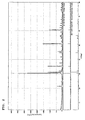
- the sintered body was target I formed of an oxide containing In and Sm as main components ( FIG. 1 ).
- ICP Inductively Coupled Plasma
- the dispersion condition of In and Sm was examined by an in-plane element distribution analysis by means of an EPMA (Electron Probe Micro Analyzer). In and Sm were dispersed substantially homogeneously. The relative density of the sintered body was 95%.
- a sintered body was obtained in the same manner as in Example 1, except that 850 g of indium oxide and 150 g of samarium oxide were used.
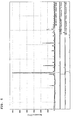
- An X-ray diffraction analysis confirmed that the resulting sintered body was target I formed of InSmO 3 and indium oxide ( FIG. 2 ).
- the dispersion condition of In and Sm was examined by an EPMA measurement. In and Sm each had a substantially uniform particle size. The relative density of the sintered body was 95%.
- the molded product was subsequently compacted at a pressure of 4 t/cm 2 by means of a cold isostatic pressing machine, fired at 1300°C and 1000 kgf/cm 2 for 3 hours by hot isostatic pressing to obtain a sintered body.
- An X-ray diffraction analysis revealed that the resulting sintered body was formed of Sn 2 Sm 2 O 7 and indium oxide ( FIG. 3 ).
- the dispersion condition of In, Sn and Sm was examined by an in-plane element distribution analysis by means of an EPMA, and it was found that Sn and Sm each had a particle size of 10 ⁇ m or less, and were dispersed homogeneously in the target.
- the relative density of the sintered body was 95% ( FIG. 4 ).
- a transparent conductive film was produced according to the following method.
- a substrate (a glass plate with a thickness of 1.1 mm) was placed in an RF magnetron sputtering device. The pressure inside a vacuum chamber was reduced to 5 ⁇ 10 -4 Pa or less. Thereafter, argon gas was introduced into the chamber to 3 ⁇ 10 -1 Pa. Sputtering was conducted (output: 100W, substrate temperature: room temperature), thereby to form a transparent conductive film with a thickness of 100 nm.
- An X-ray diffraction analysis confirmed that the resultant transparent conductive film was amorphous.
- the resulting transparent conductive film had a specific resistance of 480 ⁇ cm and a transmittance to visible light of 86.2%. The specific resistance was low of 485 ⁇ cm even after a 1000 hour-long humidity test at 40°C with a relative humidity of 90%. The resulting transparent conductive film was confirmed to be excellent in moisture resistance. After the heat treatment at 300°C in atmosphere for one hour, the specific resistance was lowered to 240 ⁇ cm. The X-ray diffraction analysis showed a peak derived from indium oxide, indicating that the transparent conductive film was crystalline ( FIG. 5 ).
- a sintered body was obtained in the same manner as in Example 3, except that 850 g of indium oxide, 50 g of tin oxide, and 100 g of samarium oxide were used.
- the results of the X-ray diffraction analysis confirmed that the sintered body was formed of Sn 2 Sm 2 O 7 , InSmO 3 , and indium oxide ( FIG. 6 ).
- the dispersion condition of In and Sm was examined by an in-plane element distribution analysis by an EPMA measurement, and it was found that Sn and Sm each had a particle size of 10 ⁇ m or less, and were dispersed substantially homogeneously in the target.
- the relative density of the sintered body was found to be 95%.
- a transparent conductive film was formed in the same manner as in Example 3, except that the sintered body obtained in (1) above was used as a sputtering target.
- An X-ray diffraction analysis confirmed that the resulting transparent conductive film was amorphous.
- the resulting transparent conductive film had a specific resistance of 435 ⁇ cm and a transmittance to visible light of 86.8%.
- the specific resistance was low of 462 ⁇ cm even after a 1000 hour-long humidity test at 40°C with a relative humidity of 90%.
- the resulting transparent conductive film was found to be excellent in moisture resistance.
- the transparent conductive film immediately after the film formation was placed in a vacuum chamber. After reducing the pressure to 5 ⁇ 10 -4 Pa or less, the transparent conductive film was subjected to heat treatment at 300°C for one hour in an atmosphere of argon of 0.3 Pa. As a result of X-ray diffraction analysis of the film, indium oxide crystals were observed, which confirmed that the resulting film was crystalline. After the heat treatment, the specific resistance of the transparent conductive film was decreased to 215 ⁇ cm.
- a sintered body was obtained in the same manner as in Example 3, except that 900 g of indium oxide, 50 g of tin oxide, and 50 g of samarium oxide were used.
- the results of X-ray diffraction analysis showed that the resulting sintered body was formed of Sn 2 Sm 2 O 7 and indium oxide.
- the dispersion state of In and Sm was examined by an EPMA measurement, and it was found that the particles of substantially uniform size were dispersed homogeneously.
- the relative density of the sintered body was 95%.
- a transparent conductive film was formed in the same manner as in Example 3, except that the sintered body obtained in (1) above was used as a sputtering target.
- An X-ray diffraction analysis revealed that the resulting transparent conductive film was amorphous.
- the resulting transparent conductive film had a specific resistance of 486 ⁇ cm and a transmittance to visible light of 86.4%.
- the specific resistance was low of 514 ⁇ cm even after a 1000 hour-long humidity test at 40°C with a relative humidity of 90%.
- the resulting transparent conductive film was confirmed to be excellent in moisture resistance.
- the transparent conductive film immediately after the film formation was subjected to heat treatment as in Example 4. As a result of X-ray diffraction analysis, indium oxide crystals were observed, which confirmed that the resulting film was crystalline. After the heat treatment, the specific resistance of the transparent conductive film was decreased to 247 ⁇ Cm.
- a sintered body was obtained in the same manner as in Example 3, except that 900 g of indium oxide, 90 g of tin oxide, and 10 g of samarium oxide were used.
- An X-ray diffraction analysis revealed that the resulting sintered body was formed of Sn 2 Sm 2 O 7 microcrystals and indium oxide.
- the dispersion state of In and Sm was examined by an EPMA measurement, and it was found that the particles of substantially uniform size were dispersed homogenously.
- the relative density of the sintered body was 95%.
- a transparent conductive film was produced in the same manner as in Example 3, except that the sintered body obtained in (1) above was used as a sputtering target.
- An X-ray diffraction analysis revealed that the resulting transparent conductive film was amorphous.
- the resulting transparent conductive film had a specific resistance of 386 ⁇ cm and a transmittance to visible light of 87.8%.
- the specific resistance was low of 432 ⁇ cm even after a 1000 hour-long humidity test at 40°C with a relative humidity of 90%.
- the resulting transparent conductive film was confirmed to be excellent in moisture resistance.
- the transparent conductive film immediately after the film formation was subjected to heat treatment as in Example 4. As a result of X-ray diffraction analysis, indium oxide crystals were observed, which confirmed the resulting film was crystalline. After the heat treatment, the specific resistance of the transparent conductive film was decreased to 195 ⁇ cm.
- a sintered body was produced in the same manner as in Example 3, except that 900 g of indium oxide and 100 g of tin oxide were used. An X-ray diffraction analysis revealed that the sintered body was formed of indium oxide of In 2 O 3 . The dispersion state of In and Sn was observed by an EPMA measurement, and it was found that the particles of substantially uniform size were dispersed homogeneously. The relative density of the sintered body was 95%.
- a transparent conductive film was produced in the same manner as in Example 3, except that the sintered body obtained in (1) above was used as a sputtering target.
- An X-ray diffraction analysis revealed that the resulting transparent conductive film was microcrystalline.
- the resulting transparent conductive film had a specific resistance of 860 ⁇ cm and a transmittance to visible light of 87.3%.
- the specific resistance was high of 1560 ⁇ cm after a 1000 hour-long humidity test at 40°C with a relative humidity of 90%.
- the resulting transparent conductive film was confirmed to be inferior in moisture resistance.
- the transparent conductive film immediately after the film formation was subjected to heat treatment as in Example 4.
- heat treatment As a result of X-ray diffraction analysis, indium oxide crystals were observed, which confirmed that the resulting film was crystalline.
- the specific resistance of the transparent conductive film was decreased to 360 ⁇ cm.
- Table 1 Sputtering target Starting material Oxide constituting target Doping element Concentration of doping element Sn/(In+Sn+Sm) (at.%) Sm/(In+Sm) Density (%)
- Example 1 Indium Oxide 450 g Samarium Oxide 550 g InSmO 3 Indium Oxide - - 0.5 95
- Example 2 Indium Oxide 850 g Samarium Oxide 150 g InSmO 3 Indium Oxide - - 0.12 95
- Example 3 Indium Oxide 900 g Tin Oxide 70 g Samarium Oxide 30 g Sn 2 Sm 2 O 7 Indium Oxide Sn 6.5 0.026 95
- Example 4 Indium Oxide 850 g Tin Oxide 50 g Samarium Oxide 100 g InSmO 3 Sn 2 Sm 2 O 7 Indium Oxide Sn 4.7 0.086 95
- Example 5 Indium Oxide 900 g Tin Oxide 50 g Samarium Oxide 50 g Sn 2 Sm 2
- Table 2 Transparent conductive film Properties of target Properties of thin film Bulk resistance of target (m ⁇ cm) Extraordinary discharge during sputtering Specific resistance ( ⁇ cm) Specific resistance after moisture resistance test ( ⁇ cm) Specific resistance after heat treatment ( ⁇ cm) Transmittance to visible rays (%)
- Example 3 1.6 None 480 485 240 86.2
- Example 4 1.5 None 435 462 215 86.8
- Example 5 1.6 None 486 514 247 86.4
- Example 6 1.3 None 386 432 195 87.8 Comparative Example 1 0.2 Occurred 860 1560 360 87.3
- the target of the invention is suitable for use as a target for producing transparent conductive films for various applications such as liquid crystal display elements, EL display elements, and solar cells.
Landscapes
- Chemical & Material Sciences (AREA)
- Engineering & Computer Science (AREA)
- Ceramic Engineering (AREA)
- Organic Chemistry (AREA)
- Materials Engineering (AREA)
- Manufacturing & Machinery (AREA)
- Structural Engineering (AREA)
- Mechanical Engineering (AREA)
- Metallurgy (AREA)
- Chemical Kinetics & Catalysis (AREA)
- Inorganic Chemistry (AREA)
- Physics & Mathematics (AREA)
- Thermal Sciences (AREA)
- Physical Vapour Deposition (AREA)
- Compositions Of Oxide Ceramics (AREA)
Abstract
Description
- The invention relates to a sputtering target and a method for producing the same.
- Recently, displays have shown remarkable progress. A variety of displays are briskly introduced to OA apparatuses such as PCs and word processors. These displays each have a structure in which a display element is interposed between transparent conductive films.
- Currently, indium tin oxide (ITO) films constitute the mainstream of conductive transparent films since ITO films have excellent transparency, low resistance, improved etching properties, good adhesion to a substrate, as well as other qualities. Generally, ITO films are prepared by sputtering.
- However, due to a relatively low moisture resistance, ITO films have such a disadvantage that the electric resistance value thereof increases by moisture. In addition, an ITO target which is used for producing an ITO film by sputtering tends to blacken by reduction. Therefore, changes in the properties of an ITO target with time have become a problem to overcome.
- A transparent conductive film formed of indium oxide and zinc oxide which is superior to ITO films in moisture resistance, and has conductivity and light transmittance almost equivalent to that of ITO films, as well as a sputtering target formed of indium oxide and zinc oxide suitable for obtaining such transparent conductive film have been proposed (Patent Documents 1 and 2).
- However, the transparent conductive film formed of indium oxide and zinc oxide is very prone to be etched by a weak acid. In addition, this film may be etched by an etching solution for a thin metal film. Therefore, in etching a thin metal film on the transparent conductive film, this transparent conductive film may also be etched. For this reason, this transparent conductive film is not suited for applications where a thin metal film on the transparent conductive film is selectively etched.
- On the other hand, a transparent conductive film containing indium oxide and a lanthanide element is known to be useful as an electrode for organic EL devices or semi-transparent/semi-reflective LCDs.
An oxide of a lanthanide element has, however, no conductivity. Therefore, when a target is formed by mixing such an oxide with indium oxide, a target with a low conductivity is obtained. In addition, this target may encounter such problems as occurrence of extraordinary discharge during sputtering or blackening of the target surface. These problems cause the sputtering speed to be lowered. -
- Patent Document 1:
JP-A-6-234565 - Patent Document 2:
JP-A-7-235219 - Patent Document 3:
JP-A-2004-68054 - Patent Document 4:
JP-A-2004-119272 - Patent Document 5:
JP-A-2004-139780 - Patent Document 6:
JP-A-2004-146136 - Patent Document 7:
JP-A-2004-158315 - Patent Document 8:
JP-A-2004-240091 - Patent Document 9:
JP-A-2004-294630 - Patent Document 10:
JP-A-2004-333882 - An object of the invention is to provide a sputtering target which has a high conductivity and is free from problems such as extraordinary discharge or blackening of the target surface.
- The invention provides the following sputtering target (hereinafter often to be referred to simply as "target").
- 1. A sputtering target which is formed of a sintered body comprising an oxide of which the main components are In and Sm.
- 2. The sputtering target according to 1, wherein the oxide comprises InSmO3 and indium oxide.
- 3. The sputtering target according to 1 or 2, wherein the atomic ratio of In and Sm, [Sm/(In+Sm)], in the sintered body is 0.001 to 0.8.
- 4. The sputtering target according to any one of 1 to 3, wherein the sintered body is doped with at least one element with an atomic valency of positive tetravalency or higher in an amount of 20 at.% or less relative to the total sum of all cation elements.
- 5. The sputtering target according to 4, wherein the element with an atomic valency of positive tetravalency or higher is one or more element selected from the group consisting of Sn, Ge, Ti, Zr, Hf, Nb and Ce.
- 6. The sputtering target according to 4 or 5 which is formed of a sintered body comprising an oxide comprising InSmO3 and/or Sn2Sm2O7.
- 7. A method for producing the sputtering target according to any one of 1 to 3 which comprises the steps of:
- mixing an indium compound and a samarium compound to obtain a mixture;
- molding the mixture to obtain a molded article; and
- sintering the molded article to obtain a sintered body.
- 8. A method for producing the sputtering target according to any one of 4 to 6 which comprises the steps of:
- adding at least one element with an atomic valency of positive tetravalency or higher to an indium compound and a samarium compound to obtain a mixture;
- molding the mixture to obtain a molded article; and
- sintering the molded article to obtain a sintered body.
- According to the invention, a sputtering target which has a high conductivity and is free from problems such as extraordinary discharge and target surface blackening irrespective of the presence of samarium (lanthanide element) can be provided.
-
-
FIG. 1 is an X-ray diffraction pattern of target I obtained in Example 1; -
FIG. 2 is an X-ray diffraction pattern of target I obtained in Example 2; -
FIG. 3 is an X-ray diffraction pattern of target II obtained in Example 3; -
FIG. 4 is a view showing an in-plane distribution measured by an EPMA of target II obtained in Example 3; -
FIG. 5 is an X-ray diffraction pattern of a transparent conductive film after heat treatment obtained in Example 3; and -
FIG. 6 is an X-ray diffraction pattern of target II obtained in Example 4. - A first target of the invention is formed of a sintered body containing an oxide, the main components of which are In and Sm (hereinafter referred to as "target I").
- The oxide comprising In and Sm as main components can contain indium oxide and samarium oxide, which are raw materials, as well as an indium-samarium oxide such as InSmO3.
- The sintered body contains an oxide comprising In and Sm as the main components preferably in an amount of 1 wt% or more, more preferably 3 wt% or more. If the content of the oxide comprising In and Sm as the main component is less than 1 wt%, conductivity may be lowered.
- Preferred examples of the oxide constituting the sintered body include the following:
- (a) InSmO3
- (b) A mixture of InSmO3 and In2O3
- (c) A mixture of InSmO3 and Sm2O3
Here, In2O3 and Sm2O3 in (b) and (c) may have either a specific crystalline structure or an amorphous structure.
Of these, a sintered body comprising (b) (mixture of InSmO3 and In2O3) is preferable. - In target I, the atomic ratio of In and Sm, (Sm/(In+Sm), is preferably 0.001 to 0.8, more preferably 0.01 to 0.20, and particularly preferably 0.01 to 0.1. If the atomic ratio is less than 0.001, durability (acid resistance) of the transparent conductive film obtained from the target may be lowered. If the atomic ratio exceeds 0.8, the conductivity of the transparent conductive film may be lowered or lost.
- The above atomic ratio of In and Sm can be obtained by adjusting the mixing ratio of an indium compound and an samarium compound before sintering. Probably, according to the mixing ratio before sintering, an indium-samarium oxide such as InSmO3 which is formed of an indium oxide and a samarium oxide in the chemical stoichiometric ratio is generated, and remaining indium oxide and samarium oxide are present as a crystalline substance, an amorphous substance or the like.
- The relative density of the sintered body constituting target I is preferably 70% or more, more preferably 85% or more, still more preferably 90% or more. If the density of the sintered body is less than 70%, the film-forming speed may be lowered, and the target and film obtained therefrom tends to blacken. To obtain a sintered body having a high density, it is preferred that sintering be performed after molding under cold isostatic pressure (CIP) or under hot isostatic pressure (HIP) or the like.
- As mentioned above, target I of the invention is formed of a sintered body of an indium-samarium oxide. Target I formed of this sintered body is excellent in conductivity and acid resistance, and hence suitable as a sputtering target for obtaining transparent conductive films for a variety of applications, including liquid crystal display devices, EL display devices and solar cells. As compared with a target formed of In2O3 and Sm2O3, target I exhibits higher conductivity and keeps stable sputtering status without extraordinary discharge and target surface blackening. By using this target, it is possible to obtain a transparent conductive film which has conductivity and light transmittance equivalent to those of an ITO film and is suitable for use as an electrode for organic EL devices or semi-transparent/semi-reflective LCDs.
- Although target I can be produced by various methods, it is preferred that target I be produced by the method of the invention, which is described later.
- A second target of the invention is a target in which the sintered body constituting target I is doped with at least one element with an atomic valency of positive tetravalency or higher in an amount of 20 at.% or less relative to the total sum of all cation elements (hereinafter referred to as "target II").
- In target II, as examples of the element having an atomic valency of positive tetravalency or higher (hereinafter often referred to as "doping element"), Sn, Ge, Ti, Zr, Hf, Ce, Nb or the like can be exemplified. Of these, Sn is preferable. The term "total sum of all cation elements" is defined as the total amount of cation elements contained in the sintered body.
- The composition, density or the like of the indium-samarium oxide in target II is the same as that of target I, and hence, explanation is omitted here.
- The reason for limiting the ratio of the doping element to 20 at.% or less in target II is mentioned below. If the ratio of the doping element exceeds 20 at.%, a transparent conductive film obtained from this target may have lowered conductivity due to carrier scattering by ions. The amount of the doping element is preferably 10 at.% or less.
- Target II includes a target that is formed of a sintered body of an oxide containing InSmO3 and/or Sn2Sm2O7.
This oxide may also contain In2O3, Sm2O3, SnO2 or the like in addition to the oxides as mentioned above.
The preferable atomic ratio of In and Sm, (Sm/(In+Sm), is the same as that in the case of target I. - Since an element having an atomic valency of positive tetravalency or higher is doped, target II provides a transparent conductive film having conductivity higher than that of a transparent conductive film obtained by target I.
- The oxide constituting the sintered body of target II may include an oxide of a doping element in addition to the oxides contained in target I.
- As in the case of target I, target II of the invention is suitable as a sputtering target for obtaining transparent conductive films for a variety of applications including liquid crystal display devices, EL display devices, solar cells, and the like. When this target is used, high target conductivity can be attained and a stable sputtering status which is free from extraordinary discharge and target surface blackening can be maintained. As a result, a transparent conductive film having conductivity and light transmittance equivalent to that of ITO films can be obtained.
- Although target II can be produced by various methods, it is preferred that target II be produced by the method of the invention II described later.
- A first method for producing a target of the invention comprises the steps of mixing an indium compound and a samarium compound to obtain a mixture; molding the mixture to obtain a molded article; and sintering the molded article to obtain a sintered body of an oxide containing In and Sm as main components (hereinafter referred to as "method I").
- An indium compound and a samarium compound used in method I may be one which becomes an oxide or an oxide after firing (oxide precursor). Examples of the indium oxide precursor and the samarium oxide precursor include sulfides, sulfates, nitrates, halides (chloride, bromide, or the like), carbonates, organic acid salts (acetate, propionate, naphthenate, or the like), alkoxides (methoxide, ethoxide, or the like), organic metal complexes (acetylacetonate or the like) of indium and samarium.
- Of these, nitrates, organic acid salts, alkoxides, and organic metal complexes are preferable for full thermal decomposition at lower temperatures with no remaining impurities.
- In method I, an indium compound and a samarium compound are mixed at first to obtain a mixture. It is preferred that this step be performed by a solution method (co-precipitation method) or a physical mixing method. The physical mixing method described below is more preferable.
- The physical mixing method can be applied to both cases, i.e. a case where the indium compound is an indium oxide or its precursor (regardless of being soluble or hardly-soluble in water), and a case where the samarium compound is a samarium oxide or its precursor (regardless of being soluble or hardly-soluble in water). According to this method, an indium compound and a samarium compound are put in a mixing apparatus such as a ball mill, a jet mill, a pearl mill, and a bead mill, and these compounds are then mixed homogeneously. The mixing time is preferably 1 to 200 hours. If mixing is performed for less than 1 hour, it may be difficult to obtain a homogeneous mixture. A mixing time exceeding 200 hours may result in lowered productivity. It is particularly preferable to perform mixing for 3 to 120 hours.
- In method I, after mixing an indium compound and a samarium compound, the resulting mixture is preferably subjected to a calcination step before a molding step.
- Although the step of calcinating the mixture of an indium compound and a samarium compound may vary depending on temperature and time, it is preferred that calcination be conducted at 500 to 1200°C for 1 to 100 hours. If calcination is conducted at temperatures lower than 50°C or for a period of less than 1 hour, thermal decomposition or reaction of an indium compound and a samarium compound is insufficient. When calcination is conducted at temperatures higher than 1200°C or for a period longer than 100 hours, particles are sintered to be large. It is particularly preferred that calcination be performed at 800 to 1200°C for 2 to 50 hours.
- According to method I of the invention, after performing calcination as mentioned above, it is preferred that the resulting calcinated product be pulverized. If need arises, the calcinated product may be subjected to reduction treatment before or after pulverization.
- It is preferred that pulverization of the calcinated product be performed by means of a ball mill, a roll mill, a pearl mill, a jet mill, a bead mill or the like in such a manner that the particle size becomes 0.01 to 1.0 µm. If the particle size is less than 0.01 µm, the particles tend to agglomerate to make handling difficult. In addition, it is hard to obtain a dense sintered body. On the other hand, when the particle size exceeds 1.0 µm, there may be a case where a dense sintered body cannot be obtained readily. Repeated calcination and pulverization is preferable for the formation of a sintered body with a uniform composition.
- As for the method for reduction when the reduction treatment is conducted, reduction with a reductive gas, firing under vacuum, reduction with an inert gas, or the like can be used. When reduction is performed with a reductive gas, hydrogen, methane, CO, a mixed gas of these gases with oxygen, or the like can be used as the reductive gas. In the case of reduction by firing in an inert gas, nitrogen, argon, a mixed gas of these gases with oxygen, or the like can be used as the reductive gas. The reduction temperature is preferably 100 to 800°C. If reduction is performed at temperatures lower than 100°C, it may be difficult to perform reduction sufficiently. When the reduction temperature exceeds 800°C, zinc oxide may evaporate to cause the composition to be changed. It is particularly preferred that the reduction be performed at 200 to 800°C. The reduction time, which depends on the reduction temperature, is preferably 0.01 to 10 hours. If the reduction is conducted for a period shorter than 0.01 hour, it may be difficult to perform reduction sufficiently. A reduction time exceeding 10 hours is not preferable from an economical viewpoint. It is particularly preferred that the reduction be conducted for 0.05 to 5 hours.
- When an oxide is used as the starting material, the above-mentioned steps of calcination and reduction may be omitted.
- In method I of the invention, a mixture or a calcinated product obtained in the previous step is then sintered.
- Molding of the mixture or the calcinated powder is conducted by die molding, casing molding, injection molding, or the like. To obtain a sintered body with a high sintering density, it is preferred that CIP (cold isostatic pressure) molding or the like be performed, followed by sintering, which is described later. The shape of a molded article may be any shape which is suitable for use as a target. For molding, it is possible to use a molding aid such as PVA (polyvinyl alcohol), MC (methyl cellulose), polywax, oleic acid or the like.
- Sintering after molding is performed by firing under normal pressure, firing under a hot isostatic pressure (HIP), or the like. The sintering may be performed at temperatures of not less than the temperature which causes an indium compound and a samarium compound to thermally decompose to become an oxide. Generally, a sintering temperature of 800 to 1700°C is preferable. A sintering temperature exceeding 1700°C is not preferable since a samarium oxide and an indium oxide sublime to cause a change in composition. It is particularly preferred that sintering be performed at 1200 to 1600°C. Sintering time depends on sintering temperature, but is preferably 1 to 50 hours, more preferably 2 to 10 hours.
- Sintering may be conducted under a reducing atmosphere. As the reducing atmosphere, an atmosphere of a reducing gas such as H2, methane, and CO, and an atmosphere of an inert gas such as Ar and N2 can be given. In this case, samarium oxide and indium oxide tend to evaporate. To prevent this, it is desirable to perform pressure sintering such as HIP sintering.
- By conducting sintering in the above-mentioned manner, intended target I formed of a sintered body of an oxide containing In and Sm as main components can be obtained.
- A second method for producing a target of the invention comprises the steps of adding at least one compound of an element with an atomic valency of positive tetravalency or higher to an indium compound and a samarium compound to obtain a mixture; and molding the mixture to obtain a molded article; and sintering the molded article to obtain a sintered body which is doped with at least one element with an atomic valency of positive tetravalency or higher in an amount of 20 at.% or less relative to the total sum of all cation elements (hereinafter referred to as method II).
- Method II is a method suitable for obtaining target II. Method II differs from method I only in the addition of at least one compound of an element with an atomic valency of positive tetravalency or higher (Sn compounds, Ge compounds, Ti compounds, Zr compounds, Hf compounds, Ce compounds, Nb compounds, for example) to an indium compound and a samarium compound to obtain a mixture. Other steps are similar to those of method I.
- As examples of the tin compound used in method II, a tin oxide or a tin oxide precursor which becomes a tin oxide after firing can be given. Specific examples include tin acetate, tin oxalate, 2-ethylhexyl tin, tin alkoxides such as dimethoxy tin, diethoxy tin, dipropoxy tin, tetramethoxy tin, tetraethoxy tin, tetrapropoxy tin and tetrabutoxy tin, tin chloride, tin fluoride, tin nitride, and tin sulfate.
- As examples of the germanium compound, a germanium oxide or its precursor can be given. Specific examples include germanium chloride, germanium alkoxides such as tetramethoxy germanium, tetraethoxy germanium, tetrapropoxy germanium and tetrabutoxy germanium, germanium sulfate, germanium nitrate, and germanium oxalate.
- As examples of the titanium compound, titanium oxide or its precursor can be given. Specific examples include titanium chloride, titanium fluoride, titanium alkoxides such as tetramethoxy titanium, tetraethoxy titanium, tetrapropoxy titanium and tetrabutoxy titanium, titanium sulfate, and titanium hydroxide.
- As examples of the zirconium compound, zirconium oxide or its precursor can be given. Specific examples include zirconium chloride, tetramethoxy zirconium, zirconium alkoxides such as tetraethoxy zirconium, tetrapropoxy zirconium and tetrabutoxy zirconium, zirconium sulfate, zirconium nitrate, and zirconium oxalate.
- As examples of the hafnium compound, hafnium oxide or its precursor can be given. Specific examples include hafnium chloride, hafnium alkoxides such as tetramethoxy hafnium, tetraethoxy hafnium, tetrapropxy hafnium and tetrabutoxy hafnium, hafnium sulfate, hafnium nitrate, and hafnium oxalate.
- As examples of the cerium compound, cerium oxide or its precursor can be given. Specific examples include cerium chloride, cerium alkoxides such as tetramethoxy cerium, tetraethoxy cerium, tetrapropoxy cerium and tetrabutoxy cerium, cerium sulfate, cerium nitrate, and cerium oxalate.
- As examples of the niobium compound, niobium oxide or its precursor can be given. Specific examples include niobium chloride, niobium alkoxides such as tetramethoxy niobium, tetraethoxy niobium, tetrapropoxy niobium and tetrabutoxy niobium, niobium sulfate, niobium nitrate, and niobium oxalate.
- It is preferred that the amount of a compound of an element with an atomic valency of positive tetravalency or higher as the doping material (e.g. tin compounds, germanium compounds, titanium compounds, zirconium compounds, hafnium compounds and niobium compounds) be determined appropriately such that the ratio of the doping element (Sn, Ge, Ti, Zr, Hf, Nb or the like) in a target which is finally obtained becomes 20 at.% or less relative to the total sum of all cation elements, taking into account evaporation or loss of each component during the production process. If the ratio of the doping element finally exceeds 20 at.%, conductivity of the target, and the resultant transparent conductive film may be lowered due to the scattering of ions.
- Of these doping elements, Sn compounds are preferably used. In this case, Sn2Sm2O7 can be generated in the target. In addition, if the atomic ratio of added Sn is larger than the atomic ratio of Sm, relative to all cations in the target, the resistivity of the target itself can be more preferably decreased.
- According to method II, intended target II in which the sintered body is doped with a specific amount of an element with an atomic valency of positive tetravalency or higher can be obtained.
- The transparent conductive film can be obtained by sputtering the above-mentioned sputtering targets I and II. The resulting transparent conductive film is normally amorphous. However, the transparent conductive film can be crystallized by heat treatment to have a low resistance.
- The transparent conductive film is preferably amorphous and has an atomic ratio of In and Sm, [Sm/(In+Sm)], of 0.001 to 0.8. A more preferable atomic ratio is 0.005 to 0.2.
When an element with an atomic valency of positive tetravalency or higher is doped, the transparent conductive film of the invention has an atomic ratio of In and Sm, [Sm/(In+Sm)], of 0.001 to 0.2, more preferably 0.01 to 0.2. The atomic ratio of the element to the total of the element, indium and samarium (i.e. element/(In+Sm+element)) is 0.01 to 0.2, preferably 0.02 to 0.1. - The properties of targets and transparent conductive films obtained in Examples and Comparative Examples were measured as follows.
- The theoretical density was calculated from the densities of raw materials used and the mixing ratio of the raw materials. The ratio of the measured density to the theoretical density was defined as the relative density.
- The amount of each element was measured by an ICP measurement.
- The bulk resistance of the target or the specific resistance of the transparent conductive film were measured and calculated by the four probe method using a Lorester (manufactured by Mitsubishi Chemical Corporation).
- The transmittance at a wavelength of 550 nm was measured by means of a microspectrophotometer using air as reference.
- 450 g of indium oxide and 550 g of samarium oxide were dispersed in ion exchange water. The dispersion was pulverized and mixed for about 5 hours by means of a bead mill.
The resulting slurry was dried and granulated by means of a spray drier. The powder was then placed in a mold with a diameter of 10 mm, and subjected to preliminary molding at a pressure of 100 kg/cm2 using a mold pressing machine. Subsequently, the molded product was compacted at a pressure of 4 t/cm2, by means of a cold isostatic pressing machine, sintered at 1300°C for 5 hours, thereby to obtain a sintered body.
As a result of an X-ray diffraction analysis, it was confirmed that the sintered body was target I formed of an oxide containing In and Sm as main components (FIG. 1 ).
As a result of an ICP (Inductively Coupled Plasma) analysis, the atomic ratio was as follows: Sm/(In+Sm)=0.5 (In/ (In+Sm)=0.5).
The dispersion condition of In and Sm was examined by an in-plane element distribution analysis by means of an EPMA (Electron Probe Micro Analyzer). In and Sm were dispersed substantially homogeneously. The relative density of the sintered body was 95%. - A sintered body was obtained in the same manner as in Example 1, except that 850 g of indium oxide and 150 g of samarium oxide were used.
An X-ray diffraction analysis confirmed that the resulting sintered body was target I formed of InSmO3 and indium oxide (FIG. 2 ).
As a result of an ICP analysis, the atomic ratio was as follows: Sm/(In+Sm)=0.12.
The dispersion condition of In and Sm was examined by an EPMA measurement. In and Sm each had a substantially uniform particle size. The relative density of the sintered body was 95%. - 900 g of indium oxide, 70 g of tin oxide, and 30 g of samarium oxide were placed in a polyimide-made pot (volume: 10 L) together with alumina balls with a diameter of 2 mm, followed by the addition of ethanol. The resultant was pulverized and mixed for 10 hours by means of a planetary ball mill.
The powder was placed in a mold with a diameter of 4 inches, and subjected to a preliminary molding using a mold pressing machine at a pressure of 100 kg/cm2. The molded product was subsequently compacted at a pressure of 4 t/cm2 by means of a cold isostatic pressing machine, fired at 1300°C and 1000 kgf/cm2 for 3 hours by hot isostatic pressing to obtain a sintered body. An X-ray diffraction analysis revealed that the resulting sintered body was formed of Sn2Sm2O7 and indium oxide (FIG. 3 ).
As a result of an ICP analysis, the atomic ratio was as follows: Sm/(In+Sm)=0.026.
The dispersion condition of In, Sn and Sm was examined by an in-plane element distribution analysis by means of an EPMA, and it was found that Sn and Sm each had a particle size of 10 µm or less, and were dispersed homogeneously in the target. The relative density of the sintered body was 95% (FIG. 4 ). - Using the sintered body obtained in (1) above was used as a sputtering target, a transparent conductive film was produced according to the following method.
A substrate (a glass plate with a thickness of 1.1 mm) was placed in an RF magnetron sputtering device. The pressure inside a vacuum chamber was reduced to 5 × 10⁻⁴ Pa or less. Thereafter, argon gas was introduced into the chamber to 3 × 10⁻¹ Pa. Sputtering was conducted (output: 100W, substrate temperature: room temperature), thereby to form a transparent conductive film with a thickness of 100 nm.
An X-ray diffraction analysis confirmed that the resultant transparent conductive film was amorphous. As a result of an ICP analysis, the atomic ratio was as follows: Sm/(In+Sm)=0.026, In/(In+Sn+Sm)=0.910, Sn/(In+Sn+Sm)=0.065, Sm/(In+Sn+Sm)=0.025.
The resulting transparent conductive film had a specific resistance of 480 µΩcm and a transmittance to visible light of 86.2%. The specific resistance was low of 485 µΩcm even after a 1000 hour-long humidity test at 40°C with a relative humidity of 90%. The resulting transparent conductive film was confirmed to be excellent in moisture resistance. After the heat treatment at 300°C in atmosphere for one hour, the specific resistance was lowered to 240 µΩcm. The X-ray diffraction analysis showed a peak derived from indium oxide, indicating that the transparent conductive film was crystalline (FIG. 5 ). - A sintered body was obtained in the same manner as in Example 3, except that 850 g of indium oxide, 50 g of tin oxide, and 100 g of samarium oxide were used.
The results of the X-ray diffraction analysis confirmed that the sintered body was formed of Sn2Sm2O7, InSmO3, and indium oxide (FIG. 6 ).
As a result of an ICP analysis, the atomic ratio was as follows: Sm/(In+Sm)=0.086.
The dispersion condition of In and Sm was examined by an in-plane element distribution analysis by an EPMA measurement, and it was found that Sn and Sm each had a particle size of 10 µm or less, and were dispersed substantially homogeneously in the target. The relative density of the sintered body was found to be 95%. - A transparent conductive film was formed in the same manner as in Example 3, except that the sintered body obtained in (1) above was used as a sputtering target.
An X-ray diffraction analysis confirmed that the resulting transparent conductive film was amorphous. As a result of an ICP analysis, the atomic ratio was as follows: Sm/(In+Sm)=0.086, In/(In+Sn+Sm)=0.87, Sn/(In+Sn+Sm)=0.047, Sm/(In+Sn+Sm)=0.083.
The resulting transparent conductive film had a specific resistance of 435 µΩcm and a transmittance to visible light of 86.8%. The specific resistance was low of 462 µΩcm even after a 1000 hour-long humidity test at 40°C with a relative humidity of 90%. The resulting transparent conductive film was found to be excellent in moisture resistance.
The transparent conductive film immediately after the film formation was placed in a vacuum chamber. After reducing the pressure to 5 × 10⁻⁴ Pa or less, the transparent conductive film was subjected to heat treatment at 300°C for one hour in an atmosphere of argon of 0.3 Pa. As a result of X-ray diffraction analysis of the film, indium oxide crystals were observed, which confirmed that the resulting film was crystalline. After the heat treatment, the specific resistance of the transparent conductive film was decreased to 215 µΩcm. - A sintered body was obtained in the same manner as in Example 3, except that 900 g of indium oxide, 50 g of tin oxide, and 50 g of samarium oxide were used.
The results of X-ray diffraction analysis showed that the resulting sintered body was formed of Sn2Sm2O7 and indium oxide.
As a result of an ICP analysis, the atomic ratio was as follows: Sm/(In+Sm)=0.042.
The dispersion state of In and Sm was examined by an EPMA measurement, and it was found that the particles of substantially uniform size were dispersed homogeneously. The relative density of the sintered body was 95%. - A transparent conductive film was formed in the same manner as in Example 3, except that the sintered body obtained in (1) above was used as a sputtering target.
An X-ray diffraction analysis revealed that the resulting transparent conductive film was amorphous. As a result of an ICP analysis, the atomic ratio was as follows: Sm/(In+Sm)=0.042, In/(In+Sn+Sm)=0.91, Sn/(In+Sn+Sm)=0.05, Sm/(In+Sn+Sm)=0.04.
The resulting transparent conductive film had a specific resistance of 486 µΩcm and a transmittance to visible light of 86.4%. The specific resistance was low of 514 µΩcm even after a 1000 hour-long humidity test at 40°C with a relative humidity of 90%. The resulting transparent conductive film was confirmed to be excellent in moisture resistance.
The transparent conductive film immediately after the film formation was subjected to heat treatment as in Example 4. As a result of X-ray diffraction analysis, indium oxide crystals were observed, which confirmed that the resulting film was crystalline. After the heat treatment, the specific resistance of the transparent conductive film was decreased to 247 µΩCm. - A sintered body was obtained in the same manner as in Example 3, except that 900 g of indium oxide, 90 g of tin oxide, and 10 g of samarium oxide were used.
An X-ray diffraction analysis revealed that the resulting sintered body was formed of Sn2Sm2O7 microcrystals and indium oxide.
As a result of an ICP analysis, the atomic ratio was as follows: Sm/(In+Sm)=0.009
The dispersion state of In and Sm was examined by an EPMA measurement, and it was found that the particles of substantially uniform size were dispersed homogenously.
The relative density of the sintered body was 95%. - A transparent conductive film was produced in the same manner as in Example 3, except that the sintered body obtained in (1) above was used as a sputtering target.
An X-ray diffraction analysis revealed that the resulting transparent conductive film was amorphous. As a result of an ICP analysis, the atomic ratio was as follows: Sm/(In+Sm)=0.0088, In/(In+Sn+Sm)=0.908, Sn/(In+Sn+Sm)=0.084, Sm/(In+Sn+Sm)=0.008
The resulting transparent conductive film had a specific resistance of 386 µΩcm and a transmittance to visible light of 87.8%. The specific resistance was low of 432 µΩcm even after a 1000 hour-long humidity test at 40°C with a relative humidity of 90%. The resulting transparent conductive film was confirmed to be excellent in moisture resistance.
The transparent conductive film immediately after the film formation was subjected to heat treatment as in Example 4. As a result of X-ray diffraction analysis, indium oxide crystals were observed, which confirmed the resulting film was crystalline. After the heat treatment, the specific resistance of the transparent conductive film was decreased to 195 µΩcm. - A sintered body was produced in the same manner as in Example 3, except that 900 g of indium oxide and 100 g of tin oxide were used.
An X-ray diffraction analysis revealed that the sintered body was formed of indium oxide of In2O3.
The dispersion state of In and Sn was observed by an EPMA measurement, and it was found that the particles of substantially uniform size were dispersed homogeneously. The relative density of the sintered body was 95%. - A transparent conductive film was produced in the same manner as in Example 3, except that the sintered body obtained in (1) above was used as a sputtering target.
An X-ray diffraction analysis revealed that the resulting transparent conductive film was microcrystalline.
As a result of an ICP analysis, the atomic ratio was as follows: In/(In+Sn)=0.91, Sn/(In+Sn)=0.09.
The resulting transparent conductive film had a specific resistance of 860 µΩcm and a transmittance to visible light of 87.3%. The specific resistance was high of 1560 µΩcm after a 1000 hour-long humidity test at 40°C with a relative humidity of 90%. The resulting transparent conductive film was confirmed to be inferior in moisture resistance.
The transparent conductive film immediately after the film formation was subjected to heat treatment as in Example 4. As a result of X-ray diffraction analysis, indium oxide crystals were observed, which confirmed that the resulting film was crystalline. After the heat treatment, the specific resistance of the transparent conductive film was decreased to 360 µΩcm. -
Table 1: Sputtering target Starting material Oxide constituting target Doping element Concentration of doping element Sn/(In+Sn+Sm) (at.%) Sm/(In+Sm) Density (%) Example 1 Indium Oxide 450 g Samarium Oxide 550 g InSmO3 Indium Oxide - - 0.5 95 Example 2 Indium Oxide 850 g Samarium Oxide 150 g InSmO3 Indium Oxide - - 0.12 95 Example 3 Indium Oxide 900 g Tin Oxide 70 g Samarium Oxide 30 g Sn2Sm2O7 Indium Oxide Sn 6.5 0.026 95 Example 4 Indium Oxide 850 g Tin Oxide 50 g Samarium Oxide 100 g InSmO3 Sn2Sm2O7 Indium Oxide Sn 4.7 0.086 95 Example 5 Indium Oxide 900 g Tin Oxide 50 g Samarium Oxide 50 g Sn2Sm2O3 Indium Oxide Indium Oxide Sn 4.7 0.042 95 Example 6 Indium Oxide 900 g Tin Oxide 90 g Samarium Oxide 10 g Sn2Sm2O7 (microcrystal) Indium Oxide Sn 8.4 0.009 95 Comparative Example 1 Indium Oxide 900 g Tin Oxide 100 g In2O3 Sn 9.3 - 95 -
Table 2: Transparent conductive film Properties of target Properties of thin film Bulk resistance of target (mΩcm) Extraordinary discharge during sputtering Specific resistance (µΩcm) Specific resistance after moisture resistance test (µΩcm) Specific resistance after heat treatment (µΩcm) Transmittance to visible rays (%) Example 3 1.6 None 480 485 240 86.2 Example 4 1.5 None 435 462 215 86.8 Example 5 1.6 None 486 514 247 86.4 Example 6 1.3 None 386 432 195 87.8 Comparative Example 1 0.2 Occurred 860 1560 360 87.3 - The target of the invention is suitable for use as a target for producing transparent conductive films for various applications such as liquid crystal display elements, EL display elements, and solar cells.
Claims (8)
- A sputtering target which is formed of a sintered body comprising an oxide of which the main components are In and Sm.
- The sputtering target according to claim 1, wherein the oxide comprises InSmO3 and indium oxide.
- The sputtering target according to claim 1 or 2, wherein the atomic ratio of In and Sm, [Sm/(In+Sm)], in the sintered body is 0.001 to 0.8.
- The sputtering target according to any one of claims 1 to 3, wherein the sintered body is doped with at least one element with an atomic valency of positive tetravalency or higher in an amount of 20 at.% or less relative to the total sum of all cation elements.
- The sputtering target according to claim 4, wherein the element with an atomic valency of positive tetravalency or higher is one or more element selected from the group consisting of Sn, Ge, Ti, Zr, Hf, Nb and Ce.
- The sputtering target according to claim 4 or 5 which is formed of a sintered body comprising an oxide comprising InSmO3 and/or Sn2Sm2O7.
- A method for producing the sputtering target according to any one of claims 1 to 3 which comprises the steps of:mixing an indium compound and a samarium compound to obtain a mixture;molding the mixture to obtain a molded article; andsintering the molded article to obtain a sintered body.
- A method for producing the sputtering target according to any one of claims 4 to 6 which comprises the steps of:adding at least one element with an atomic valency of positive tetravalency or higher to an indium compound and a samarium compound to obtain a mixture;molding the mixture to obtain a molded article; andsintering the molded article to obtain a sintered body.
Applications Claiming Priority (3)
| Application Number | Priority Date | Filing Date | Title |
|---|---|---|---|
| JP2005207513 | 2005-07-15 | ||
| JP2005258740 | 2005-09-07 | ||
| PCT/JP2006/312412 WO2007010702A1 (en) | 2005-07-15 | 2006-06-21 | In Sm OXIDE SPUTTERING TARGET |
Publications (3)
| Publication Number | Publication Date |
|---|---|
| EP1905864A1 true EP1905864A1 (en) | 2008-04-02 |
| EP1905864A4 EP1905864A4 (en) | 2008-07-23 |
| EP1905864B1 EP1905864B1 (en) | 2013-06-12 |
Family
ID=37668587
Family Applications (1)
| Application Number | Title | Priority Date | Filing Date |
|---|---|---|---|
| EP06767071.1A Not-in-force EP1905864B1 (en) | 2005-07-15 | 2006-06-21 | In Sm OXIDE SPUTTERING TARGET |
Country Status (6)
| Country | Link |
|---|---|
| US (1) | US7648657B2 (en) |
| EP (1) | EP1905864B1 (en) |
| JP (1) | JP5089386B2 (en) |
| KR (1) | KR101294986B1 (en) |
| TW (1) | TWI390064B (en) |
| WO (1) | WO2007010702A1 (en) |
Cited By (1)
| Publication number | Priority date | Publication date | Assignee | Title |
|---|---|---|---|---|
| CN111943649A (en) * | 2020-07-22 | 2020-11-17 | 长沙壹纳光电材料有限公司 | Sintered body for vapor deposition and preparation method thereof |
Families Citing this family (9)
| Publication number | Priority date | Publication date | Assignee | Title |
|---|---|---|---|---|
| US8038911B2 (en) * | 2006-08-10 | 2011-10-18 | Idemitsu Kosan Co., Ltd. | Lanthanoid-containing oxide target |
| KR20090063946A (en) * | 2007-12-14 | 2009-06-18 | 삼성코닝정밀유리 주식회사 | Indium tin oxide target and manufacturing method of transparent conductive film using same |
| KR102801852B1 (en) | 2011-06-08 | 2025-04-28 | 가부시키가이샤 한도오따이 에네루기 켄큐쇼 | Sputtering target, method for manufacturing sputtering target, and method for forming thin film |
| US9885108B2 (en) | 2012-08-07 | 2018-02-06 | Semiconductor Energy Laboratory Co., Ltd. | Method for forming sputtering target |
| JP6141777B2 (en) | 2013-02-28 | 2017-06-07 | 株式会社半導体エネルギー研究所 | Method for manufacturing semiconductor device |
| KR102340437B1 (en) | 2013-12-27 | 2021-12-16 | 이데미쓰 고산 가부시키가이샤 | Oxide sintered body, method for producing same and sputtering target |
| US11274363B2 (en) * | 2019-04-22 | 2022-03-15 | Nxp Usa, Inc. | Method of forming a sputtering target |
| CN114477997A (en) * | 2020-05-20 | 2022-05-13 | 深圳市科思飞科技有限公司 | Ceramic powder and application thereof |
| CN116283291B (en) * | 2023-03-20 | 2024-02-23 | 中国矿业大学(北京) | Insulation tube preparation method |
Family Cites Families (19)
| Publication number | Priority date | Publication date | Assignee | Title |
|---|---|---|---|---|
| JPS5385400A (en) * | 1977-01-06 | 1978-07-27 | Tdk Corp | Porcelain composite for voltage non-linear resistor |
| JPS6450258A (en) * | 1987-08-21 | 1989-02-27 | Sumitomo Metal Mining Co | Production of thin film of high-refractive index dielectric material |
| JPS6450258U (en) | 1987-09-22 | 1989-03-28 | ||
| JP2695605B2 (en) | 1992-12-15 | 1998-01-14 | 出光興産株式会社 | Target and manufacturing method thereof |
| US5972527A (en) | 1992-12-15 | 1999-10-26 | Idemitsu Kosan Co., Ltd. | Transparent electrically conductive layer, electrically conductive transparent substrate and electrically conductive material |
| JP3179287B2 (en) | 1993-12-28 | 2001-06-25 | 出光興産株式会社 | Conductive transparent substrate and method for producing the same |
| JP3803132B2 (en) * | 1996-01-31 | 2006-08-02 | 出光興産株式会社 | Target and manufacturing method thereof |
| JP4308497B2 (en) | 2002-10-16 | 2009-08-05 | 出光興産株式会社 | Electrode substrate for organic electroluminescence device, organic electroluminescence device and method for producing the device |
| JP2004119272A (en) | 2002-09-27 | 2004-04-15 | Idemitsu Kosan Co Ltd | Organic el device and substrate used for it |
| JP4448648B2 (en) * | 2002-08-02 | 2010-04-14 | 出光興産株式会社 | A conductive film manufactured using a sputtering target and a sintered body. |
| CN102522509B (en) | 2002-08-02 | 2016-01-20 | 出光兴产株式会社 | Sputtering target, sintered body, conductive film produced using the same, organic EL element, and substrate used for the same |
| JP4241003B2 (en) | 2002-11-07 | 2009-03-18 | 出光興産株式会社 | Electrode substrate for organic electroluminescence device and organic EL light emitting device |
| JP4428502B2 (en) | 2002-10-23 | 2010-03-10 | 出光興産株式会社 | Electrode substrate for organic electroluminescent element, method for producing the same, and organic EL light emitting device |
| JP2004240091A (en) | 2003-02-05 | 2004-08-26 | Idemitsu Kosan Co Ltd | Method for manufacturing transflective electrode substrate |
| JP2004333882A (en) | 2003-05-08 | 2004-11-25 | Idemitsu Kosan Co Ltd | Reflective electrode substrate and method of manufacturing the same |
| WO2004070812A1 (en) * | 2003-02-05 | 2004-08-19 | Idemitsu Kosan Co.,Ltd. | Method for manufacturing semi-transparent semi-reflective electrode substrate, reflective element substrate, method for manufacturing same, etching composition used for the method for manufacturing the reflective electrode substrate |
| JP2004294630A (en) | 2003-03-26 | 2004-10-21 | Idemitsu Kosan Co Ltd | Reflective electrode substrate, method of manufacturing the same, and etching composition used in the method of manufacturing the same |
| JP4281390B2 (en) * | 2003-03-28 | 2009-06-17 | 株式会社デンソー | Insulating layer and method of manufacturing electroluminescent device |
| JP4762062B2 (en) * | 2006-06-22 | 2011-08-31 | 出光興産株式会社 | Sintered body, film, and organic electroluminescence element |
-
2006
- 2006-06-21 EP EP06767071.1A patent/EP1905864B1/en not_active Not-in-force
- 2006-06-21 WO PCT/JP2006/312412 patent/WO2007010702A1/en not_active Ceased
- 2006-06-21 KR KR1020087001015A patent/KR101294986B1/en not_active Expired - Fee Related
- 2006-06-21 JP JP2007525917A patent/JP5089386B2/en not_active Expired - Fee Related
- 2006-06-21 US US11/995,640 patent/US7648657B2/en not_active Expired - Fee Related
- 2006-06-27 TW TW095123205A patent/TWI390064B/en not_active IP Right Cessation
Cited By (2)
| Publication number | Priority date | Publication date | Assignee | Title |
|---|---|---|---|---|
| CN111943649A (en) * | 2020-07-22 | 2020-11-17 | 长沙壹纳光电材料有限公司 | Sintered body for vapor deposition and preparation method thereof |
| CN111943649B (en) * | 2020-07-22 | 2022-08-26 | 长沙壹纳光电材料有限公司 | Sintered body for vapor deposition and preparation method thereof |
Also Published As
| Publication number | Publication date |
|---|---|
| WO2007010702A1 (en) | 2007-01-25 |
| TWI390064B (en) | 2013-03-21 |
| US20090121199A1 (en) | 2009-05-14 |
| EP1905864A4 (en) | 2008-07-23 |
| JP5089386B2 (en) | 2012-12-05 |
| US7648657B2 (en) | 2010-01-19 |
| KR101294986B1 (en) | 2013-08-08 |
| KR20080026169A (en) | 2008-03-24 |
| JPWO2007010702A1 (en) | 2009-01-29 |
| EP1905864B1 (en) | 2013-06-12 |
| TW200712232A (en) | 2007-04-01 |
Similar Documents
| Publication | Publication Date | Title |
|---|---|---|
| EP1408137B1 (en) | Sputtering target for the deposition of a transparent conductive film | |
| JP4850378B2 (en) | Sputtering target, transparent conductive oxide, and method for producing sputtering target | |
| JP3179287B2 (en) | Conductive transparent substrate and method for producing the same | |
| EP2278041B1 (en) | Sputtering target and transparent conductive film obtainable by the target | |
| JP5269501B2 (en) | Oxide sintered body and sputtering target comprising the same | |
| JP3746094B2 (en) | Target and manufacturing method thereof | |
| EP2428500B1 (en) | Indium oxide sintered body, indium oxide transparent conductive film, and method for manufacturing the transparent conductive film | |
| JP4960244B2 (en) | Oxide material and sputtering target | |
| JP2695605B2 (en) | Target and manufacturing method thereof | |
| KR101168447B1 (en) | Indium oxide/zinc oxide/magnesium oxide sputtering target and transparent conductive film | |
| EP1905864B1 (en) | In Sm OXIDE SPUTTERING TARGET | |
| EP2573059A1 (en) | Sintered zinc oxide tablet and process for producing same | |
| JP5377328B2 (en) | Tin oxide-magnesium oxide sputtering target and transparent semiconductor film | |
| EP2327673A1 (en) | Oxide sintered compact for producing transparent conductive film | |
| EP1422316A1 (en) | Method for cleaning reaction container and film deposition system | |
| CN101223296A (en) | In·Sm Oxide Sputtering Target | |
| US20110114475A1 (en) | Method for producing transparent conductive film | |
| JP2010269984A (en) | Method for producing ZnO-based sintered body containing boron | |
| JP2012140673A (en) | Zinc oxide based transparent conductive film forming material, method for producing the material, target using the material, and method for forming zinc oxide based transparent conductive film | |
| JP2012140276A (en) | Zinc oxide-based transparent conductive film forming material, target using the same, method for forming zinc oxide-based transparent conductive film, and transparent conductive substrate | |
| JP2012142535A (en) | Patterning method |
Legal Events
| Date | Code | Title | Description |
|---|---|---|---|
| PUAI | Public reference made under article 153(3) epc to a published international application that has entered the european phase |
Free format text: ORIGINAL CODE: 0009012 |
|
| 17P | Request for examination filed |
Effective date: 20071217 |
|
| AK | Designated contracting states |
Kind code of ref document: A1 Designated state(s): DE FR GB NL |
|
| DAX | Request for extension of the european patent (deleted) | ||
| RIN1 | Information on inventor provided before grant (corrected) |
Inventor name: YANO, KOKI Inventor name: TANAKA, NOBUO Inventor name: INOUE, KAZUYOSHI Inventor name: TOMAI, SHIGEKAZU Inventor name: KAIJO, AKIRA Inventor name: MATSUBARA, MASATO |
|
| A4 | Supplementary search report drawn up and despatched |
Effective date: 20080624 |
|
| RBV | Designated contracting states (corrected) |
Designated state(s): DE FR GB NL |
|
| 17Q | First examination report despatched |
Effective date: 20080917 |
|
| DAX | Request for extension of the european patent (deleted) | ||
| REG | Reference to a national code |
Ref country code: DE Ref legal event code: R079 Ref document number: 602006036781 Country of ref document: DE Free format text: PREVIOUS MAIN CLASS: C23C0014340000 Ipc: C23C0014080000 |
|
| RIC1 | Information provided on ipc code assigned before grant |
Ipc: C04B 35/645 20060101ALI20121126BHEP Ipc: C23C 14/34 20060101ALI20121126BHEP Ipc: C04B 35/00 20060101ALI20121126BHEP Ipc: C04B 35/01 20060101ALI20121126BHEP Ipc: C04B 35/50 20060101ALI20121126BHEP Ipc: C04B 35/626 20060101ALI20121126BHEP Ipc: C23C 14/08 20060101AFI20121126BHEP Ipc: C04B 35/457 20060101ALI20121126BHEP |
|
| GRAP | Despatch of communication of intention to grant a patent |
Free format text: ORIGINAL CODE: EPIDOSNIGR1 |
|
| GRAS | Grant fee paid |
Free format text: ORIGINAL CODE: EPIDOSNIGR3 |
|
| GRAA | (expected) grant |
Free format text: ORIGINAL CODE: 0009210 |
|
| AK | Designated contracting states |
Kind code of ref document: B1 Designated state(s): DE FR GB NL |
|
| REG | Reference to a national code |
Ref country code: GB Ref legal event code: FG4D |
|
| REG | Reference to a national code |
Ref country code: DE Ref legal event code: R096 Ref document number: 602006036781 Country of ref document: DE Effective date: 20130808 |
|
| REG | Reference to a national code |
Ref country code: NL Ref legal event code: VDEP Effective date: 20130612 |
|
| PG25 | Lapsed in a contracting state [announced via postgrant information from national office to epo] |
Ref country code: NL Free format text: LAPSE BECAUSE OF FAILURE TO SUBMIT A TRANSLATION OF THE DESCRIPTION OR TO PAY THE FEE WITHIN THE PRESCRIBED TIME-LIMIT Effective date: 20130612 |
|
| PLBE | No opposition filed within time limit |
Free format text: ORIGINAL CODE: 0009261 |
|
| STAA | Information on the status of an ep patent application or granted ep patent |
Free format text: STATUS: NO OPPOSITION FILED WITHIN TIME LIMIT |
|
| 26N | No opposition filed |
Effective date: 20140313 |
|
| REG | Reference to a national code |
Ref country code: DE Ref legal event code: R097 Ref document number: 602006036781 Country of ref document: DE Effective date: 20140313 |
|
| PGFP | Annual fee paid to national office [announced via postgrant information from national office to epo] |
Ref country code: GB Payment date: 20140618 Year of fee payment: 9 |
|
| PGFP | Annual fee paid to national office [announced via postgrant information from national office to epo] |
Ref country code: DE Payment date: 20140618 Year of fee payment: 9 |
|
| PGFP | Annual fee paid to national office [announced via postgrant information from national office to epo] |
Ref country code: FR Payment date: 20140609 Year of fee payment: 9 |
|
| REG | Reference to a national code |
Ref country code: DE Ref legal event code: R119 Ref document number: 602006036781 Country of ref document: DE |
|
| GBPC | Gb: european patent ceased through non-payment of renewal fee |
Effective date: 20150621 |
|
| REG | Reference to a national code |
Ref country code: FR Ref legal event code: ST Effective date: 20160229 |
|
| PG25 | Lapsed in a contracting state [announced via postgrant information from national office to epo] |
Ref country code: GB Free format text: LAPSE BECAUSE OF NON-PAYMENT OF DUE FEES Effective date: 20150621 Ref country code: DE Free format text: LAPSE BECAUSE OF NON-PAYMENT OF DUE FEES Effective date: 20160101 |
|
| PG25 | Lapsed in a contracting state [announced via postgrant information from national office to epo] |
Ref country code: FR Free format text: LAPSE BECAUSE OF NON-PAYMENT OF DUE FEES Effective date: 20150630 |