EP1903776A2 - Imaging apparatus, method for driving the same and radiation imaging system - Google Patents
Imaging apparatus, method for driving the same and radiation imaging system Download PDFInfo
- Publication number
- EP1903776A2 EP1903776A2 EP07115298A EP07115298A EP1903776A2 EP 1903776 A2 EP1903776 A2 EP 1903776A2 EP 07115298 A EP07115298 A EP 07115298A EP 07115298 A EP07115298 A EP 07115298A EP 1903776 A2 EP1903776 A2 EP 1903776A2
- Authority
- EP
- European Patent Office
- Prior art keywords
- read out
- sampling
- holding
- pixels
- imaging apparatus
- Prior art date
- Legal status (The legal status is an assumption and is not a legal conclusion. Google has not performed a legal analysis and makes no representation as to the accuracy of the status listed.)
- Granted
Links
Images


Classifications
-
- H—ELECTRICITY
- H04—ELECTRIC COMMUNICATION TECHNIQUE
- H04N—PICTORIAL COMMUNICATION, e.g. TELEVISION
- H04N5/00—Details of television systems
- H04N5/30—Transforming light or analogous information into electric information
- H04N5/32—Transforming X-rays
-
- H—ELECTRICITY
- H04—ELECTRIC COMMUNICATION TECHNIQUE
- H04N—PICTORIAL COMMUNICATION, e.g. TELEVISION
- H04N25/00—Circuitry of solid-state image sensors [SSIS]; Control thereof
- H04N25/60—Noise processing, e.g. detecting, correcting, reducing or removing noise
- H04N25/67—Noise processing, e.g. detecting, correcting, reducing or removing noise applied to fixed-pattern noise, e.g. non-uniformity of response
- H04N25/671—Noise processing, e.g. detecting, correcting, reducing or removing noise applied to fixed-pattern noise, e.g. non-uniformity of response for non-uniformity detection or correction
- H04N25/677—Noise processing, e.g. detecting, correcting, reducing or removing noise applied to fixed-pattern noise, e.g. non-uniformity of response for non-uniformity detection or correction for reducing the column or line fixed pattern noise
-
- H—ELECTRICITY
- H04—ELECTRIC COMMUNICATION TECHNIQUE
- H04N—PICTORIAL COMMUNICATION, e.g. TELEVISION
- H04N25/00—Circuitry of solid-state image sensors [SSIS]; Control thereof
- H04N25/70—SSIS architectures; Circuits associated therewith
- H04N25/71—Charge-coupled device [CCD] sensors; Charge-transfer registers specially adapted for CCD sensors
- H04N25/75—Circuitry for providing, modifying or processing image signals from the pixel array
-
- H—ELECTRICITY
- H04—ELECTRIC COMMUNICATION TECHNIQUE
- H04N—PICTORIAL COMMUNICATION, e.g. TELEVISION
- H04N25/00—Circuitry of solid-state image sensors [SSIS]; Control thereof
- H04N25/70—SSIS architectures; Circuits associated therewith
- H04N25/76—Addressed sensors, e.g. MOS or CMOS sensors
- H04N25/767—Horizontal readout lines, multiplexers or registers
-
- H—ELECTRICITY
- H04—ELECTRIC COMMUNICATION TECHNIQUE
- H04N—PICTORIAL COMMUNICATION, e.g. TELEVISION
- H04N25/00—Circuitry of solid-state image sensors [SSIS]; Control thereof
- H04N25/70—SSIS architectures; Circuits associated therewith
- H04N25/76—Addressed sensors, e.g. MOS or CMOS sensors
Definitions
- the present invention relates to an imaging apparatus, a method for driving the same and a radiation imaging system suitably applicable to medical diagnosis and industrial non-destructive inspection.
- radiation includes electromagnetic waves, X-rays, ⁇ -rays, ⁇ -rays and ⁇ -rays.
- Radiographing a moving image needs to ensure a high frame rate as is not the case with photographing a still image.
- cardioangiography requires a frame rate of 30 FPS depending on the part and the purpose of radiographing. For this reason, in radiographing a moving image, "pixel addition" is performed in which a plurality of pixels on plural rows and/or plural columns is simultaneously read out to improve an S/N ratio and to further increase the frame rate.
- a patient In radiographing by a radiation imaging apparatus, particularly in radiographing a moving image, a patient needs to be irradiated with X rays for a long time.
- the exposure of the patient to radiation needs to be reduced. That is to say, the dosage of exposure to radiation per frame needs to be reduced, in other words, noise in an X-ray imaging apparatus needs to be reduced, which is a problem to be solved.
- noise includes components caused by so-called circuit noise such as shot noise related to dark current in a radiation detection element, thermal noise in a switching element and noise in an operational amplifier forming a read out circuit.
- circuit noise such as shot noise related to dark current in a radiation detection element, thermal noise in a switching element and noise in an operational amplifier forming a read out circuit.
- the former noise is generated independently on a pixel basis and becomes dotted noise concerning graininess in an image, which is referred to as "random noise.”
- the latter noise affects the pixels and is not an independent generating phenomenon on a pixel basis.
- This noise commonly acts particularly on signal wirings (read out wirings) to affect image quality.
- driving the apparatus so that signals from a plurality of pixels in the row direction are simultaneously read out into the signal wirings (read out wirings) in the column direction brings about a peculiar horizontal linear artifact (in the row direction). This is referred to as "line noise.”
- a random noise Nr in a radiation imaging apparatus having M-row and N-column pixels is represented by a standard deviation of M ⁇ N dark pixel data if noise included in the pixels is independently generated.
- the random noise Nr cannot be calculated by a standard deviation of dark pixel data obtained once.
- dark pixel data is obtained twice and the standard deviations of data subjected to subtraction process respectively are calculated and divided by ( ⁇ 2) to calculate the random noise Nr.
- the line noise Nl is obtained by calculating a standard deviation of M pieces of data in which average value is calculated on a row basis. If a peculiar fixed pattern noise exists in the read out circuit unit or pixels, the standard deviation may be similarly divided by ( ⁇ 2).
- the line noise is a characteristic horizontal linear artifact and may more significantly degrade image quality as compared with the random noise Nr.
- the line noise Nl becomes less conspicuous on an image.
- U.S. Patent No. 6,952,015 describes that the line noise Nl is ⁇ Nr/10. Incidentally, it is extremely difficult to reduce the line noise Nl.
- a noise source resulting in the line noise includes for example a sensor bias source for supplying a bias to a radiation detection element. Variation in the sensor bias source for some reason generates noise on the read out wiring through the capacitance of the radiation detection unit connected between the sensor bias source and read out wiring. Typically, the sensor bias sources are capacitively coupled to the read out wirings inside the radiation detection unit. Variation in the sensor bias sources causes noise to get into the read out wirings. Furthermore, signals from the pixels are sampled and held in a capacitive element Cn for sampling and holding. Noise components caused by variation in the sensor bias sources are also sampled and held along with the signals in synchronization with a control signal instructing the timing of sampling and holding.
- a noise source resulting in the line noise includes for example a power supply connected to the read out circuit unit.
- An operational amplifier provided in the read out circuit unit generally has an index of a power supply rejection ratio (PSRR).
- PSRR power supply rejection ratio
- Variation in power supply for supplying voltage for operating the read out circuit unit and in power supply for supplying reference voltage to the operational amplifier of the read out circuit unit for some reason varies the output line of the operational amplifier An.
- the noise components generated by the variation are also sampled and held in synchronization with the control signal instructing the timing of sampling and holding.
- variation in power supply of the radiation detection unit and the read out circuit unit samples and holds part of the variation in synchronization with the control signal instructing the timing of sampling and holding.
- U.S. Patent No. 6,952,015 discloses that lowpass filters are provided between a radiation detection unit and a power supply therefor and between a read out circuit unit and a power supply therefor to decrease noise components getting into the radiation detection unit or the read out circuit unit from the power supply.
- a noise source resulting in the line noise includes, for example, an externally originated noise source existing outside the radiation generating apparatus.
- the externally originated noise source includes, for example, a high voltage power source of a radiation generating apparatus, an ignition coil of a vehicle, a thunderbolt phenomenon, a motor driving in the neighbor and MRI and CT device operated in the next room in the hospital.
- the externally originated noise from the externally originated noise source propagates through space, transmitted into the read out wiring and GND line, and sampled and held in a capacitive element at timing of the control signal instructing the timing of sampling and holding with signals from pixels.
- the above externally originated noise superimposes the line noise onto the output signal (Vout) output from the amplifier.
- the externally originated noise turns into a horizontal linear line noise in the row direction to significantly degrade image quality.
- dosage of exposure to radiation X-ray dose
- X-ray dose is a little to cause a problem in that the line noise becomes conspicuous.
- U.S. Patent Application Publication No. 2003/0190088 discloses an imaging apparatus in which a line noise detecting unit for detecting whether a line noise exists from the imaging output of a two dimensional area sensor stored in a memory circuit is provided to calculate the output quantity of the line noise, remove the line noise from the imaging output and correct the imaging output.
- the output of the line noise is calculated from the average of the row output.
- the line noise generated on a row basis may have shading. In this case, correct correction value as the quantity of line noise to be corrected may not be indicated. If a calculation method in consideration of the above-mentioned is used and if it takes a long time to calculate, a problem arises in that it becomes difficult to correct the line noise in real time. A complicated algorithm has a drawback in that the load of apparatus development becomes large to increase the cost.
- U.S. Patent No. 6,734,414 discloses an imaging apparatus in which a gate wiring is connected to pixels not on a row basis but at random.
- a horizontal linear line noise will not be generated on the principle of wiring.
- output signal charges are not regular and it is required to rearrange signals in the processing circuit at the rear stage, which complicates processing.
- the gate wiring is complicated, which may decrease a production yield to cause a problem of an increase in cost.
- the present invention has been made in view of the above-mentioned problems and has for its purpose to provide a radiation imaging apparatus capable of reducing an extremely conspicuous line noise appearing in a picked up image with a simple configuration without complicating the configuration of an apparatus, a method of driving the same and a radiation imaging system.
- An imaging apparatus of the present invention has a detection unit including a plurality of pixels arranged in row and column directions, wherein each of the pixels includes a conversion element for converting an incident radiation or an incident light into an electric charge and a switch element for transferring an electric signal corresponding to the electric charge, a drive circuit unit for driving a plurality of the switch elements arranged in the row direction to transfer the electric signals in parallel from the pixels arranged in the row direction, a read out circuit unit for reading out the electric signals in parallel, wherein the read out circuit unit comprises a first sampling and holding circuit for sampling and holding an electric signal from pixels arranged along one column of the detection unit, and a second sampling and holding circuit for sampling and holding and an electric signal from pixels arranged along another column of the detection unit, and a control unit for controlling the read out circuit unit, such that the first and second sampling and holding circuits perform the sampling and holding in mutually different timings.
- a radiation imaging system of the present invention has the radiation imaging apparatus and a radiation generating apparatus for emitting the radiation to the detection unit.
- a method for driving a radiation imaging apparatus of the present invention having a detection unit including a plurality of pixels arranged in row and column directions, wherein each of the pixels includes a conversion element for converting an incident radiation or an incident light into an electric charge and a switch element for transferring an electric signal corresponding to the electric charge, a drive circuit unit for driving a plurality of the switch elements arranged in the row direction to transfer the electric signals in parallel from the pixels arranged in the row direction, and a read out circuit unit for reading out the electric signals in parallel, wherein the read out circuit unit comprises a first sampling and holding circuit for sampling and holding an electric signal from pixels arranged along one column of the detection unit, and a second sampling and holding circuit for sampling and holding and an electric signal from pixels arranged along another column of the detection unit, the method comprises a step of controlling the read out circuit unit, such that the first and second sampling and holding circuits perform the sampling and holding in mutually different timings.
- the present invention is enabled to reduce extremely conspicuous line noise appearing in a picked up image with a simple configuration without complicating the configuration of an apparatus.
- FIG. 1 is a schematic diagram of a radiation imaging apparatus (an X ray imaging apparatus) according to a first embodiment.
- FIG. 2 is a schematic diagram illustrating one example of a detail internal configuration of the drive circuit unit illustrated in FIG. 1.
- FIG. 3 is a timing chart illustrating one example of operation of the drive circuit unit illustrated in FIG. 2.
- FIG. 4 is a timing chart illustrating one example of operation of the drive circuit unit illustrated in FIG. 2.
- FIG. 5 a timing chart illustrating one example of operation of the drive circuit unit illustrated in FIG. 2.
- FIG. 6 is a timing chart illustrating one example of operation of the radiation imaging apparatus according to the first embodiment.
- FIG. 7 is a schematic diagram of a radiation imaging apparatus (an X ray imaging apparatus) according to a second embodiment.
- FIG. 8 is a timing chart illustrating one example of operation of the radiation imaging apparatus according to the second embodiment.
- FIG. 9 is a schematic diagram of a radiation imaging apparatus (an X ray imaging apparatus) according to a third embodiment.
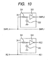
- FIG. 10 is a schematic diagram illustrating one example of a detail internal configuration of the delay circuit unit illustrated in FIG. 9.
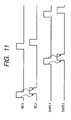
- FIG. 11 is a timing chart of the sampling and holding signals (SMPL1 and SMPL2) and reset signals (RC1 and RC2) obtained by the delay circuit units.
- FIG. 1 is a schematic diagram of a radiation imaging apparatus (an X ray imaging apparatus) according to a first embodiment.
- the radiation imaging apparatus according to the first embodiment includes a radiation detection unit 10 for detecting an incident radiation, drive circuit unit 20 for driving the pixels 11 of the radiation detection unit 10, read out circuit unit 30 for reading out electric charges (or electric signals) from the pixels 11 and control unit 40 for controlling the operation of the drive circuit unit 20 and the read out circuit unit 30.
- a plurality of the pixels 11 is arranged two-dimensionally in row and column directions on the radiation detection unit 10.
- 36 pixels 11 (6 ⁇ 6, 6 channels) are illustrated in FIG. 1, actually however, the radiation detection unit 10 is formed of multiple channels including much more pixels.
- radiation detection elements (or conversion elements) S1-1 to S6-6 convert an incident radiation into an electric charge and are biased by sensor bias sources 12.
- Switch elements T1-1 to T6-6 transfer electric signals corresponding to the electric charges of the radiation detection elements S1-1 to S6-6 to the read out circuit unit 30 and are formed of thin film transistors (TFT), for example.
- Gate wirings (or drive wirings) G1 to G6 serve to drive the switch elements T1-1 to T6-6 and are arranged to be commonly connected to the switch elements of a plurality of the pixels in the row direction.
- Read out wirings M1 to M6 serve to read out electric signals corresponding to the electric charges of the radiation detection elements S1-1 to S6-6 through the switch elements T1-1 to T6-6 and are arranged to be commonly connected to the switch elements of a plurality of the pixels in the column direction.
- the radiation detection elements S1-1 to S6-6 are categorized into two types: direct and indirect conversion type.
- a radiation detection element of the direct conversion type is formed of, for instance, amorphous selenium, lead iodide, mercuric iodide, cadmium telluride, gallium arsenide, gallium phosphide or zinc sulfide as a main ingredient and directly converts an incident radiation (X ray) into an electric signal by the main ingredient.
- a radiation detection element of the indirect conversion type includes phosphor (or a wavelength converter) for converting an incident radiation (X ray) into a visible ray and a photoelectric conversion element for converting the visible ray converted by the phosphor into an electric charge (or an electric signal).
- the phosphor in the radiation detection element of the indirect conversion type is arranged in substantially close contact with the photoelectric conversion element.
- the phosphor is formed of, for example, Gd 2 O 2 S, Gd 2 O 3 or CsI as a main ingredient.
- the photoelectric conversion element is formed of, for example, amorphous silicon as a main ingredient.
- the switch elements T1-1 to T6-6 are driven by the drive circuit unit 20 through the gate wirings G1 to G6 in the row direction.
- the read out wirings M1 to M6 are connected to the read out circuit 30.
- the electric signals of the radiation detection elements S1-1 to S6-6 are read out by the read out circuit unit 30 through the read out wirings M1 to M6.
- the pixel 11 includes a single radiation detection element, a single switch element and a single sensor bias source 12.
- Operational amplifiers A1 to A6 function as integrators by configuring capacitive elements CF1 to CF6 as illustrated in FIG. 1. Switches SW1 to SW6 reset integral charges of the capacitive elements CF1 to CF6 according to RC control signals.
- Capacitive elements C1 to C6 sample and hold the electric signals of the operational amplifiers A1 to A6. Turning on or off switches Sn1 to Sn6 samples and holds the electric signals.
- the switch Sn1 and the capacitive element C1 form a sampling and holding circuit corresponding to the read out wiring M1 and the switch Sn2 and the capacitive element C2 form a sampling and holding circuit corresponding to the read out wiring M2.
- These sampling and holding circuits equal in number to the read out wirings altogether form a sampling and holding circuit unit.
- the switches Sn1, Sn3 and Sn5 out of the switches Sn1 to Sn6 are turned on or off by an SMPL1 control signal of a control unit 40.
- the switches Sn2, Sn4 and Sn6 out of the switches Sn1 to Sn6 are turned on or off by an SMPL2 control signal of the control unit 40.
- Buffer amplifiers B1 to B6 correctly transfer the electric potentials of the capacitive elements C1 to C6. Applying signals from a shift register 31 to switches Sr1 to Sr6 converts the parallel signals of the buffer amplifiers B1 to B6 into series signals and the series signals are output through an amplifier 32.
- the present embodiment is characterized in that add channels (or, add read out wirings M1, M3 and M5) and even channels (or, even read out wirings M2, M4 and M6) are independently controlled by the SMPL1 and the SMPL2 control signals respectively. That is to say, the channels can be controlled in a temporally offset manner.
- FIG. 2 is a schematic diagram of one example of a detail internal configuration of the drive circuit unit 20 illustrated in FIG. 1.
- the drive circuit unit 20 includes a plurality of D flip-flops 21, a plurality of AND elements 22 and level shift circuits 23. Configuring each constituent as illustrated in FIG. 2 forms the drive circuit unit 20.
- the drive circuit unit 20 is controlled by three control signals OE, SIN and Sclk from the control unit 40.
- the D flip-flop 21 and the AND element 22 are digital circuits.
- the input and output voltages thereof are related to processes for producing the constituents.
- the input and the output voltage of a logic Hi have been a five-volt system, however, a recent requirement for low consumption power and advancement in process technique have released a device operating by a 3.3-volt system or by a voltage lower than that.
- the switches for the radiation detection unit 10 are formed of, for example, amorphous silicon as a main gradient.
- the drive voltage thereof is desirably five volts or higher in a current process technique for producing a TFT made of amorphous silicon.
- the level shift circuit 23 is provided to convert a drive voltage into one having a voltage level adapted to the characteristic of TFT made of amorphous silicon.
- FIGS. 3 to 5 are timing charts illustrating one example of operation of the drive circuit unit 20 illustrated in FIG. 2 respectively.
- FIG. 3 illustrates the case where the outputs of gate wirings G1 to G6 in the level shift circuit 23 are shifted step by step according to the Sclk control signal.
- FIG. 4 illustrates the case where the gate wirings G1 and G2 are simultaneously driven in the level shift circuit 23, then the gate wirings G3 and G4 are simultaneously driven, and then the gate wirings G5 and G6 are simultaneously driven according to the Sclk control signal.
- the operation illustrated in FIG. 4 intends to perform an operation at the time of reading out the signal charges of the pixels illustrated in FIG. 1 with two pixels added in a column direction . In this case, a pixel pitch is as large as two times and a drive time is halved.
- FIG. 5 illustrates the case where the gate wirings G1 to G3 are simultaneously driven in the level shift circuit 23 and then the gate wirings G4 to G6 are simultaneously driven according to the Sclk control signal.
- This operation intends to perform an operation at the time of reading out the signal charges of the pixels with three pixels added in the row direction. In this case, a pixel pitch is as large as three times and a drive time is reduced to a third.
- FIG. 6 is a timing chart illustrating one example of operation of the radiation imaging apparatus according to the first embodiment.
- the switch elements T1-1 to T1-6 on the first row are turned on by the drive signal from the drive circuit unit 20 to the gate wiring G1.
- the signal charges photoelectrically converted by the radiation detection elements S1-1 to S1-6 on the first row are read out through the read out wirings M1 to M6 and input into the read put circuit unit 30.
- the signal charges on the first row photoelectrically converted by the radiation detection elements S1-1 to S1-6 are input into the operational amplifiers A1 to A6 respectively (transfer operation).
- the signal charges input into the operational amplifiers A1 to A6 are stored in the capacitive elements CF1 to CF6.
- the SMPL1 and the SMPL2 control signals are input from the control unit 40 in different timing periods and the signal charges are collectively transferred to the capacitive elements C1 to C6 for sampling and holding respectively.
- the switches Sr1 to Sr6 receive from the shift register 31 signals for causing the switches Sr1 to Sr6 to be sequentially turned on, parallel data in the signals of the capacitive elements C1 to C6 are rearranged into series data in time-series to be output from the amplifier 32 as analog signals for one row (series conversion operation).
- the operation related to the pixels on the second row in the radiation detection unit 10 is described.
- the signal charges related to the pixels on the first row are sampled and held in the capacitive elements C1 to C6 by the SMPL1 and the SMPL2 control signals and thereafter the transfer operation is allowed of the signal charges related to the pixels on the second row.
- the capacitive elements CF1 to CF6 are reset by the RC control signal and thereafter the transfer operation is performed by driving the gate wiring G2 and then the foregoing series conversion operation is performed.
- the same operation is repeated related to the pixels on the third row and the following. That is to say, in the configuration illustrated in FIG. 1, the presence of the sampling and holding circuit simultaneously enables the transfer operation on the n-th row and the series conversion operation on the (n + 1)-th row.
- the SMPL1 and the SMPL2 control signals are supplied from the control unit 40 and independently control the odd channels (or, the odd read out wirings M1, M3 and M5) and the even channels (or, the even read out wirings M2, M4 and M6) respectively.
- timing in sampling and holding is offset between the odd and the even channels so that the quantity of noise superimposed on the odd and the even channels is different.
- the timing in sampling and holding is offset to cause the sampling and holding operation of the odd and the even channels to be independent.
- the frequency range of externally originated noise and power supply noise is from the pulse width of sampling and holding to the order of one-line operating time, the quantities of noise superimposed on the odd and the even channels are different, so that line noise exerts less influence, producing an excellent image with less line noise.
- externally originated noise and power supply noise which are sufficiently longer in time range (low frequency) as compared with one-line operating time are small in separation of noise superimposed on the odd and the even channels, which is less effective for improvement in image quality.
- the externally originated noise and power supply noise are generally transferred in an alternating-current phenomenal manner, so that the action of an image on a black and a white side is randomly superimposed between the odd and the even channel to reduce a horizontal linear artifact (or line noise).
- the random noise Nr in the radiation imaging apparatus with M-row and N-column pixels is represented by standard deviation of M ⁇ N dark pixel data if noises included in the pixels are independently generated.
- the random noise Nr cannot be calculated by standard deviation of dark pixel data obtained at one time.
- dark pixel data is obtained twice and the standard deviations of the data subjected to subtraction process respectively are calculated and divided by ( ⁇ 2) to obtain the random noise Nr.
- the line noise Nl is obtained by calculating the standard deviations of M pieces of data in which average value is calculated on a row basis. If a peculiar fixed pattern noise exists in the read out circuit unit or the pixels, the standard deviation may be similarly divided by ( ⁇ 2).
- the random noise Nr and the line noise Nl are different in source from each other.
- the line noise Nl is more sensitive than the random noise Nr in image quality.
- the line noise Nl is caused by the sampling and holding operation and reset operation being performed on a line (row) basis. Our experience indicates that if Nl ⁇ Nr/10, the line noise Nl becomes inconspicuous on an image and is not a problem any longer.
- the quantity of line noise in itself only on the odd channel is not reduced and the quantity of line noise in itself only on the even channel is not reduced either. If they are independent, the line noise is equal to Nl/( ⁇ 2) for the case where the line noise is calculated on a row basis.
- the present embodiment it is enabled to reduce extremely conspicuous line noise appearing on a picked up image with a simple configuration without complicating the configuration of the apparatus.
- the relation on timing between the SMPL1 and the SMPL2 control signals being the sampling and holding signals is the same on a row basis.
- the relation on timing between the SMPL1 and the SMPL2 control signals may be changed every row, for example.
- the control signals may be fed into the sampling and holding circuits corresponding to the predetermined read out wirings and into the sampling and holding circuits corresponding to read out wirings different from the predetermined read out wirings respectively such that the sampling and holding circuits perform the sampling and holding in mutually different timings.
- the timing may be different at the start of the sampling and holding or at the end of the sampling and holding.
- the drive circuit unit 20 may simultaneously input the drive signals into n-gate wirings G1 to G6 (where, n ⁇ 2).
- the pixels connected to the n-drive wirings are simultaneously driven, and the read out circuit unit 30 reads out added electric charges (or electric signals) in the n-pixels per each read out wiring.
- sampling and holding signals are separated into two systems of the odd and the even channels and input, the following mode may be used.
- N is taken to be a natural number and the control unit 40 inputs the sampling and holding signals different in drive timing from each other into three systems of read out wirings (3N) column, (3N-1) column and (3N-2) column. This enables further enhancing an effect of reduction in line noise.
- N is taken to be a natural number and the control unit 40 inputs the sampling and holding signals different in drive timing from each other into four systems of read out wirings (4N) column, (4N-1) column, (4N-2) column and (4N-3) column. This enables still further enhancing an effect of reduction in line noise.
- a plurality of analog multiplexers including the shift register 31 and the switches Sr1 to Sr6 are provided, and the control unit 40 inputs the sampling and holding signals different in drive timing from each other into each of the analog multiplexers. This enables further enhancing an effect of reduction in line noise.
- a plurality of the read out wirings is separated into a plurality of read out wiring groups.
- Control signals for controlling the read out circuit unit 30 may be fed into the read out circuit unit 30 such that the sampling and holding circuits corresponding to the predetermined read out wiring groups and the sampling and holding circuits corresponding to read out wiring groups different from the predetermined read out wiring groups perform the sampling and holding in mutually different timings.
- control wirings for the control signals input from the control unit 40 are more effective for an improvement in image quality, however, providing the control wirings in a blind way increases the area of the read out circuit unit 30, resulting in decrease in yield. This also complicates the control by the control unit 40, which may increase the cost of the apparatus.
- the appropriate number of the systems is up to four with consideration for the above.
- FIG. 7 is a schematic diagram of a radiation imaging apparatus (an X ray imaging apparatus) according to the second embodiment.
- the same constituents as those of the first embodiment are denoted by the same reference characters and numbers, and detailed description thereof is omitted because functions thereof are the same as those described in the first embodiment.
- the second embodiment is different from the first embodiment in the configuration of the read out circuit unit 230.
- the odd and the even channels are independently controlled by the SMPL1 and the SMPL2 control signals respectively, and in addition to the above, the odd and the even channels are independently controlled by the RC1 and the RC2 control signal respectively. That is, when reset is performed, the control unit 40 inputs the RC1 control signal into the odd channel of the read out circuit unit 230 and the RC2 control signal into the even channel thereof. By shifting reset timings, reset operations of the odd and even channels are set as independent events.
- FIG. 8 is a timing chart illustrating one example of operation of the radiation imaging apparatus according to the second embodiment.
- FIG. 8 illustrates an example where an externally originated noise gets into the apparatus.
- the RC1 and the RC2 control signal are supplied from the control unit 40 for controlling timing for operating the apparatus and independently control the odd and the even channels respectively.
- the timing in sampling and holding and in reset is offset so that the quantity of noise superimposed on the odd and the even channels is different, thereby reducing the line noise to improve image quality.
- the read out circuit unit 230 is driven based on the SMPL1 and the SMPL2 control signals, so that the line noises different in quantity between the odd and the even channels are superimposed on the output signal on the third row.
- the read out circuit unit 230 is driven based on the RC1 and the RC2 control signals, so that line noises different in quantity between the odd and the even channels are superimposed on the output signal on the six row.
- the timing chart is drawn with the signal components included, so that the line noises are indicated by broken lines.
- Line noises generated by sources of noise caused by variation in the power supplies of the radiation detection unit 10 and the read out circuit unit 230 and sources of noise passing through space are a phenomenon independent from reset by the RC1 and the RC2 and the sampling and holding by the SMPL1 and the SMPL2. It is unclear whether or not the line noise is on the white side or on the black side.
- a noteworthy distinction for the present embodiment is that both the sampling and holding operations and both the reset operations between the odd and the even channels are separated and independently operated, thereby stochastically improving image quality.
- the reset operation and the sampling and holding operation are operated in different timing between the odd and the even channels. This may increase the possibility of dispersion of the noises superimposed on the odd and the even channels as compared with the case of the first embodiment to allow extremely conspicuous line noises appearing on a pickup image to be reduced.
- the relation on timing between the SMPL1 and the SMPL2 control signals being sampling and holding signals and the relation on timing between the RC1 and the RC2 control signals being reset signals are the same on a row basis.
- the relation on timing between the SMPL1 and the SMPL2 control signals and between the RC1 and the RC2 control signals may be changed every row, for example. That is to say, in the present embodiment, the control signals may be fed into the reset unit corresponding to the predetermined read out wirings and the reset unit corresponding to read out wirings different from the predetermined read out wirings such that the reset units reset in mutually different timings.
- the timing may be different at the start of the reset or at the end of the reset.
- the drive circuit unit 20 may simultaneously input the drive signals into n-gate wirings G1 to G6 (where, n ⁇ 2).
- the pixels connected to the n-drive wirings are simultaneously driven, and the read out circuit unit 230 reads out added electric charges (or electric signals) in the n-pixels per each read out wiring.
- sampling and holding signals and the reset signals are separated into two systems of the odd and the even channels and input, the following mode may be used.
- N is taken to be a natural number and the control unit 40 inputs the sampling and holding signals and the reset signals different in drive timing from each other into three systems of read out wirings (3N) column, (3N-1) column and (3N-2) column. This enables further enhancing an effect of reduction in line noise.
- N is taken to be a natural number and the control unit 40 inputs the sampling and holding signals and the reset signals different in drive timing from each other into four systems of read out wirings (4N) column, (4N-1) column, (4N-2) column and (4N-3) column. This enables still further enhancing an effect of reduction in line noise.
- a plurality of analog multiplexers including the shift register 31 and the switches Sr1 to Sr6 are provided, and the control unit 40 inputs the sampling and holding signals and the reset signals different in drive timing from each other into each of the analog multiplexers. This enables further enhancing an effect of reduction in line noise.
- a plurality of read out wirings is separated into a plurality of read out wiring groups.
- Control signals for controlling the read out circuit unit 230 may be fed into the read out circuit unit 30 such that the reset unit corresponding to the predetermined read out wiring groups and the reset unit corresponding to read out wiring groups different from the predetermined read out wiring groups reset in mutually different timings.
- FIG. 9 is a schematic diagram of a radiation imaging apparatus (an X ray imaging apparatus) according to the third embodiment.
- the same constituents as those of the first embodiment are denoted by the same reference characters and numbers, and detailed description thereof is omitted because functions thereof are the same as those described in the first embodiment.
- the third embodiment is different from the first and the second embodiment in the configuration of the read out circuit unit 330.
- the inputs into the sampling and holding control signal and the reset control signal are taken to be a single respectively in contrast to the second embodiment illustrated in FIG. 7, and the sampling and holding control signal and the reset control signal are separated into two systems of the odd and the even channels respectively by using delay circuit units 33 and 34 provided inside the read out circuit unit 330.
- FIG. 10 is a schematic diagram illustrating of one example of a detail internal configuration of the delay circuit units 33 and 34 illustrated in FIG. 9.
- the delay circuit unit 33 includes a resistor 331, capacitive element 332 and buffer 333, and similarly the delay circuit unit 34 includes a resistor 341, capacitive element 342 and buffer 343.
- the SMPL control signal input from the control unit 40 passes through a primary LPF formed of the resistor 331 and capacitive element 332, thereafter it is shaped into a rectangular wave by the digital buffer 333 and turns into the SMPL2 control signal in the second embodiment.
- the SMPL control signal input from the control unit 40 turns into the SMPL1 control signal in the second embodiment without processed as it is.
- the RC control signal input from the control unit 40 passes through a primary LPF formed of the resistor 341 and capacitive element 342, thereafter it is shaped into a rectangular wave by the digital buffer 343 and turns into the RC2 control signal in the second embodiment.
- the RC control signal input from the control unit 40 turns into the RC1 control signal in the second embodiment without processed as it is.
- FIG. 11 is a timing chart of the sampling and holding signals (SMPL1 and SMPL2) and reset signals (RC1 and RC2) obtained by the delay circuit units 33 and 34.
- the delay circuit units 33 and 34 delay both rise and fall of the SMPL2 and the RC2 control signals with respect to the SMPL1 and the RC1 control signals.
- the fourth embodiment of the present invention is described below.
- the fourth embodiment provides a radiation imaging system including the radiation imaging apparatus according to the foregoing first to third embodiments.
- the radiation imaging system according to the fourth embodiment includes at least any of the radiation imaging apparatus according to the first to third embodiments and a radiation generating apparatus for emitting radiation (X rays) to the radiation detection unit 10 of the radiation imaging apparatus.
- the units illustrated in FIGS. 1, 7 and 9 forming the radiation imaging apparatus according to the above embodiments and the steps illustrated in FIG. 3 to 6, 8 and 11 describing a method for driving the radiation imaging apparatus can be realized by operating the programs stored in a RAM and ROM of a computer.
- the programs and the computer readable storage media for storing the programs are included in the present invention.
- the programs are stored in storage media such as, for example, a CD-ROM or supplied to a computer via various transmission media.
- storage media such as, for example, a CD-ROM or supplied to a computer via various transmission media.
- a flexible disk, hard disk, magnetic tape, magnetooptical disk and non-volatile memory card may be used as storage media for storing the programs in addition to the CD-ROM.
- communication media in a computer network system LAN, WAN such as the Internet and radio communication network
- the communication media in this case include a wired line such as an optical fiber and a radio line.
- the programs are included in the present invention for the cases where a computer executes a supplied program to realize functions of the radiation imaging apparatus according to the embodiments, the programs realize functions of the radiation imaging apparatus according to the embodiments in collaboration with an operating system (OS) or other application software operating in a computer, and a feature expansion board and a feature expansion unit of the computer perform all or part of processes of the supplied programs to realize functions of the radiation imaging apparatus according to the embodiments.
- OS operating system
- a feature expansion board and a feature expansion unit of the computer perform all or part of processes of the supplied programs to realize functions of the radiation imaging apparatus according to the embodiments.
- the present invention can be suitably used in an imaging apparatus, radiation imaging apparatus, a method for driving the same and a radiation imaging system suitably applicable to medical diagnosis and industrial non-destructive inspection.
- an imaging apparatus For reducing extremely conspicuous line noise appearing in a picked up image with a simple configuration without complicating the configuration of an apparatus, an imaging apparatus a first sampling and holding circuit (Sn1,C1) for sampling and holding an electric signal from pixels (11) in one column of the detection unit (10) and a second sampling and holding circuit (Sn2,C2) for sampling and holding and electric signal from pixels (11) in the other column of the detection unit (10), and a control unit (40) for controlling such that the first and second sampling and holding circuits (Sn1,C1, Sn2,C2) perform the sampling and holding in mutually different timings.
Abstract
Description
- The present invention relates to an imaging apparatus, a method for driving the same and a radiation imaging system suitably applicable to medical diagnosis and industrial non-destructive inspection. In the present specification, the term "radiation" includes electromagnetic waves, X-rays, γ-rays, α-rays and β-rays.
- An FPD capable of both photographing a still image such a radiography and radiographing a moving image such as fluoroscopic radiography and angiography with a single apparatus has been proposed in recent years. Radiographing a moving image needs to ensure a high frame rate as is not the case with photographing a still image. In general, cardioangiography requires a frame rate of 30 FPS depending on the part and the purpose of radiographing. For this reason, in radiographing a moving image, "pixel addition" is performed in which a plurality of pixels on plural rows and/or plural columns is simultaneously read out to improve an S/N ratio and to further increase the frame rate.
- In radiographing by a radiation imaging apparatus, particularly in radiographing a moving image, a patient needs to be irradiated with X rays for a long time. The exposure of the patient to radiation needs to be reduced. That is to say, the dosage of exposure to radiation per frame needs to be reduced, in other words, noise in an X-ray imaging apparatus needs to be reduced, which is a problem to be solved.
- In general, noise includes components caused by so-called circuit noise such as shot noise related to dark current in a radiation detection element, thermal noise in a switching element and noise in an operational amplifier forming a read out circuit. In addition to the above, there is noise transmitted thorough signal wirings (read out wirings) from the power supply of a radiation detection element and read out circuit unit and noise components getting into the signal wirings (read out wirings) through space from external noise sources.
- The former noise is generated independently on a pixel basis and becomes dotted noise concerning graininess in an image, which is referred to as "random noise." On the other hand, the latter noise affects the pixels and is not an independent generating phenomenon on a pixel basis. This noise commonly acts particularly on signal wirings (read out wirings) to affect image quality. In particular, driving the apparatus so that signals from a plurality of pixels in the row direction are simultaneously read out into the signal wirings (read out wirings) in the column direction brings about a peculiar horizontal linear artifact (in the row direction). This is referred to as "line noise."
- In general, a random noise Nr in a radiation imaging apparatus having M-row and N-column pixels is represented by a standard deviation of M × N dark pixel data if noise included in the pixels is independently generated. However, there is peculiar fixed pattern noise resulting from a radiation detection element or switching element in a radiation detection unit, so that the random noise Nr cannot be calculated by a standard deviation of dark pixel data obtained once. Typically, dark pixel data is obtained twice and the standard deviations of data subjected to subtraction process respectively are calculated and divided by (√2) to calculate the random noise Nr.
- On the other hand, the line noise Nl is obtained by calculating a standard deviation of M pieces of data in which average value is calculated on a row basis. If a peculiar fixed pattern noise exists in the read out circuit unit or pixels, the standard deviation may be similarly divided by (√2). The line noise is a characteristic horizontal linear artifact and may more significantly degrade image quality as compared with the random noise Nr.
- If the standard deviation of the line noise Nl is expressed by Nl ≤ Nr/10, the line noise Nl becomes less conspicuous on an image. For example,
U.S. Patent No. 6,952,015 describes that the line noise Nl is ≤ Nr/10. Incidentally, it is extremely difficult to reduce the line noise Nl. - A noise source resulting in the line noise includes for example a sensor bias source for supplying a bias to a radiation detection element. Variation in the sensor bias source for some reason generates noise on the read out wiring through the capacitance of the radiation detection unit connected between the sensor bias source and read out wiring. Typically, the sensor bias sources are capacitively coupled to the read out wirings inside the radiation detection unit. Variation in the sensor bias sources causes noise to get into the read out wirings. Furthermore, signals from the pixels are sampled and held in a capacitive element Cn for sampling and holding. Noise components caused by variation in the sensor bias sources are also sampled and held along with the signals in synchronization with a control signal instructing the timing of sampling and holding.
- A noise source resulting in the line noise includes for example a power supply connected to the read out circuit unit. An operational amplifier provided in the read out circuit unit generally has an index of a power supply rejection ratio (PSRR). Variation in power supply for supplying voltage for operating the read out circuit unit and in power supply for supplying reference voltage to the operational amplifier of the read out circuit unit for some reason varies the output line of the operational amplifier An. The noise components generated by the variation are also sampled and held in synchronization with the control signal instructing the timing of sampling and holding. In other words, variation in power supply of the radiation detection unit and the read out circuit unit samples and holds part of the variation in synchronization with the control signal instructing the timing of sampling and holding.
-
U.S. Patent No. 6,952,015 discloses that lowpass filters are provided between a radiation detection unit and a power supply therefor and between a read out circuit unit and a power supply therefor to decrease noise components getting into the radiation detection unit or the read out circuit unit from the power supply. - A noise source resulting in the line noise includes, for example, an externally originated noise source existing outside the radiation generating apparatus. The externally originated noise source includes, for example, a high voltage power source of a radiation generating apparatus, an ignition coil of a vehicle, a thunderbolt phenomenon, a motor driving in the neighbor and MRI and CT device operated in the next room in the hospital. The externally originated noise from the externally originated noise source propagates through space, transmitted into the read out wiring and GND line, and sampled and held in a capacitive element at timing of the control signal instructing the timing of sampling and holding with signals from pixels.
- The above externally originated noise superimposes the line noise onto the output signal (Vout) output from the amplifier. The externally originated noise turns into a horizontal linear line noise in the row direction to significantly degrade image quality. Particularly, in radiographing a moving image, dosage of exposure to radiation (X-ray dose) is a little to cause a problem in that the line noise becomes conspicuous.
-
U.S. Patent Application Publication No. 2003/0190088 discloses an imaging apparatus in which a line noise detecting unit for detecting whether a line noise exists from the imaging output of a two dimensional area sensor stored in a memory circuit is provided to calculate the output quantity of the line noise, remove the line noise from the imaging output and correct the imaging output. - In
U.S. Patent Application Publication No. 2003/0190088 , the output of the line noise is calculated from the average of the row output. Particularly in an apparatus including a radiation detecting unit with an area as large as 40 cm × 40 cm, the line noise generated on a row basis may have shading. In this case, correct correction value as the quantity of line noise to be corrected may not be indicated. If a calculation method in consideration of the above-mentioned is used and if it takes a long time to calculate, a problem arises in that it becomes difficult to correct the line noise in real time. A complicated algorithm has a drawback in that the load of apparatus development becomes large to increase the cost. -
U.S. Patent No. 6,734,414 discloses an imaging apparatus in which a gate wiring is connected to pixels not on a row basis but at random. InU.S. Patent No. 6,734,414 , a horizontal linear line noise will not be generated on the principle of wiring. However, output signal charges are not regular and it is required to rearrange signals in the processing circuit at the rear stage, which complicates processing. Furthermore, the gate wiring is complicated, which may decrease a production yield to cause a problem of an increase in cost. - That is to say, in a radiation imaging apparatus of conventional FPD type, it has been difficult to reduce an extremely conspicuous line noise appearing in a picked up image with a simple configuration without complicating the configuration of an apparatus.
- The present invention has been made in view of the above-mentioned problems and has for its purpose to provide a radiation imaging apparatus capable of reducing an extremely conspicuous line noise appearing in a picked up image with a simple configuration without complicating the configuration of an apparatus, a method of driving the same and a radiation imaging system.
- An imaging apparatus of the present invention has a detection unit including a plurality of pixels arranged in row and column directions, wherein each of the pixels includes a conversion element for converting an incident radiation or an incident light into an electric charge and a switch element for transferring an electric signal corresponding to the electric charge, a drive circuit unit for driving a plurality of the switch elements arranged in the row direction to transfer the electric signals in parallel from the pixels arranged in the row direction, a read out circuit unit for reading out the electric signals in parallel, wherein the read out circuit unit comprises a first sampling and holding circuit for sampling and holding an electric signal from pixels arranged along one column of the detection unit, and a second sampling and holding circuit for sampling and holding and an electric signal from pixels arranged along another column of the detection unit, and a control unit for controlling the read out circuit unit, such that the first and second sampling and holding circuits perform the sampling and holding in mutually different timings.
- A radiation imaging system of the present invention has the radiation imaging apparatus and a radiation generating apparatus for emitting the radiation to the detection unit.
- A method for driving a radiation imaging apparatus of the present invention having a detection unit including a plurality of pixels arranged in row and column directions, wherein each of the pixels includes a conversion element for converting an incident radiation or an incident light into an electric charge and a switch element for transferring an electric signal corresponding to the electric charge, a drive circuit unit for driving a plurality of the switch elements arranged in the row direction to transfer the electric signals in parallel from the pixels arranged in the row direction, and a read out circuit unit for reading out the electric signals in parallel, wherein the read out circuit unit comprises a first sampling and holding circuit for sampling and holding an electric signal from pixels arranged along one column of the detection unit, and a second sampling and holding circuit for sampling and holding and an electric signal from pixels arranged along another column of the detection unit, the method comprises a step of controlling the read out circuit unit, such that the first and second sampling and holding circuits perform the sampling and holding in mutually different timings.
- According to the present invention, it is enabled to reduce extremely conspicuous line noise appearing in a picked up image with a simple configuration without complicating the configuration of an apparatus.
- Further features of the present invention will become apparent from the following description of exemplary embodiments with reference to the attached drawings.
- FIG. 1 is a schematic diagram of a radiation imaging apparatus (an X ray imaging apparatus) according to a first embodiment.
- FIG. 2 is a schematic diagram illustrating one example of a detail internal configuration of the drive circuit unit illustrated in FIG. 1.
- FIG. 3 is a timing chart illustrating one example of operation of the drive circuit unit illustrated in FIG. 2.
- FIG. 4 is a timing chart illustrating one example of operation of the drive circuit unit illustrated in FIG. 2.
- FIG. 5 a timing chart illustrating one example of operation of the drive circuit unit illustrated in FIG. 2.
- FIG. 6 is a timing chart illustrating one example of operation of the radiation imaging apparatus according to the first embodiment.
- FIG. 7 is a schematic diagram of a radiation imaging apparatus (an X ray imaging apparatus) according to a second embodiment.
- FIG. 8 is a timing chart illustrating one example of operation of the radiation imaging apparatus according to the second embodiment.
- FIG. 9 is a schematic diagram of a radiation imaging apparatus (an X ray imaging apparatus) according to a third embodiment.
- FIG. 10 is a schematic diagram illustrating one example of a detail internal configuration of the delay circuit unit illustrated in FIG. 9.
- FIG. 11 is a timing chart of the sampling and holding signals (SMPL1 and SMPL2) and reset signals (RC1 and RC2) obtained by the delay circuit units.
- The embodiments of the present invention are described in detail below with reference to the accompanying drawings.
- [First Embodiment]
- FIG. 1 is a schematic diagram of a radiation imaging apparatus (an X ray imaging apparatus) according to a first embodiment. The radiation imaging apparatus according to the first embodiment includes a
radiation detection unit 10 for detecting an incident radiation,drive circuit unit 20 for driving thepixels 11 of theradiation detection unit 10, read outcircuit unit 30 for reading out electric charges (or electric signals) from thepixels 11 andcontrol unit 40 for controlling the operation of thedrive circuit unit 20 and the read outcircuit unit 30. - A plurality of the
pixels 11 is arranged two-dimensionally in row and column directions on theradiation detection unit 10. For the sake of simplifying description, 36 pixels 11 (6 × 6, 6 channels) are illustrated in FIG. 1, actually however, theradiation detection unit 10 is formed of multiple channels including much more pixels. For example, theradiation detection unit 10 with a light receiving area of 40 cm × 40 cm needs to satisfy a resolution of substantially 200 µm pitch or lower to image the thorax of human body for medical purpose. If a light receiving area is 40 cm × 40 cm and a resolution is 200 µm pitch, the number of pixels is equal to 2000 × 2000 = 4,000,000 pixels. In this case, the number of read out wirings is 2000. Electric charges of pixels in theradiation detection unit 10 are divided to be read out by several read out circuit units. Typically, the number of channels in the read out circuit is, for example, 64, 128 or 256 and is selected according to production yield or man hour. - In FIG. 1, radiation detection elements (or conversion elements) S1-1 to S6-6 convert an incident radiation into an electric charge and are biased by sensor bias sources 12. Switch elements T1-1 to T6-6 transfer electric signals corresponding to the electric charges of the radiation detection elements S1-1 to S6-6 to the read out
circuit unit 30 and are formed of thin film transistors (TFT), for example. Gate wirings (or drive wirings) G1 to G6 serve to drive the switch elements T1-1 to T6-6 and are arranged to be commonly connected to the switch elements of a plurality of the pixels in the row direction. Read out wirings M1 to M6 serve to read out electric signals corresponding to the electric charges of the radiation detection elements S1-1 to S6-6 through the switch elements T1-1 to T6-6 and are arranged to be commonly connected to the switch elements of a plurality of the pixels in the column direction. - The radiation detection elements S1-1 to S6-6 are categorized into two types: direct and indirect conversion type. A radiation detection element of the direct conversion type is formed of, for instance, amorphous selenium, lead iodide, mercuric iodide, cadmium telluride, gallium arsenide, gallium phosphide or zinc sulfide as a main ingredient and directly converts an incident radiation (X ray) into an electric signal by the main ingredient. On the other hand, a radiation detection element of the indirect conversion type includes phosphor (or a wavelength converter) for converting an incident radiation (X ray) into a visible ray and a photoelectric conversion element for converting the visible ray converted by the phosphor into an electric charge (or an electric signal). The phosphor in the radiation detection element of the indirect conversion type is arranged in substantially close contact with the photoelectric conversion element. The phosphor is formed of, for example, Gd2O2S, Gd2O3 or CsI as a main ingredient. The photoelectric conversion element is formed of, for example, amorphous silicon as a main ingredient. The radiation detection elements both of the direct and the indirect conversion type can realize a wide and thin
radiation detection unit 10 to embody an FPD, which permits significantly reducing a time period from capture to obtainment of an image. - The switch elements T1-1 to T6-6 are driven by the
drive circuit unit 20 through the gate wirings G1 to G6 in the row direction. The read out wirings M1 to M6 are connected to the read outcircuit 30. The electric signals of the radiation detection elements S1-1 to S6-6 are read out by the read outcircuit unit 30 through the read out wirings M1 to M6. Thepixel 11 includes a single radiation detection element, a single switch element and a singlesensor bias source 12. - Operational amplifiers A1 to A6 function as integrators by configuring capacitive elements CF1 to CF6 as illustrated in FIG. 1. Switches SW1 to SW6 reset integral charges of the capacitive elements CF1 to CF6 according to RC control signals.
- Capacitive elements C1 to C6 sample and hold the electric signals of the operational amplifiers A1 to A6. Turning on or off switches Sn1 to Sn6 samples and holds the electric signals. The switch Sn1 and the capacitive element C1 form a sampling and holding circuit corresponding to the read out wiring M1 and the switch Sn2 and the capacitive element C2 form a sampling and holding circuit corresponding to the read out wiring M2. These sampling and holding circuits equal in number to the read out wirings altogether form a sampling and holding circuit unit. In the present embodiment, the switches Sn1, Sn3 and Sn5 out of the switches Sn1 to Sn6 are turned on or off by an SMPL1 control signal of a
control unit 40. The switches Sn2, Sn4 and Sn6 out of the switches Sn1 to Sn6 are turned on or off by an SMPL2 control signal of thecontrol unit 40. - Buffer amplifiers B1 to B6 correctly transfer the electric potentials of the capacitive elements C1 to C6. Applying signals from a
shift register 31 to switches Sr1 to Sr6 converts the parallel signals of the buffer amplifiers B1 to B6 into series signals and the series signals are output through anamplifier 32. - The present embodiment is characterized in that add channels (or, add read out wirings M1, M3 and M5) and even channels (or, even read out wirings M2, M4 and M6) are independently controlled by the SMPL1 and the SMPL2 control signals respectively. That is to say, the channels can be controlled in a temporally offset manner.
- The internal configuration of the
drive circuit unit 20 is described below. FIG. 2 is a schematic diagram of one example of a detail internal configuration of thedrive circuit unit 20 illustrated in FIG. 1. Thedrive circuit unit 20 includes a plurality of D flip-flops 21, a plurality of ANDelements 22 andlevel shift circuits 23. Configuring each constituent as illustrated in FIG. 2 forms thedrive circuit unit 20. - The
drive circuit unit 20 is controlled by three control signals OE, SIN and Sclk from thecontrol unit 40. In general, the D flip-flop 21 and the ANDelement 22 are digital circuits. The input and output voltages thereof are related to processes for producing the constituents. In general, the input and the output voltage of a logic Hi have been a five-volt system, however, a recent requirement for low consumption power and advancement in process technique have released a device operating by a 3.3-volt system or by a voltage lower than that. However, in general, the switches for theradiation detection unit 10 are formed of, for example, amorphous silicon as a main gradient. The drive voltage thereof is desirably five volts or higher in a current process technique for producing a TFT made of amorphous silicon. For this reason, thelevel shift circuit 23 is provided to convert a drive voltage into one having a voltage level adapted to the characteristic of TFT made of amorphous silicon. - FIGS. 3 to 5 are timing charts illustrating one example of operation of the
drive circuit unit 20 illustrated in FIG. 2 respectively. FIG. 3 illustrates the case where the outputs of gate wirings G1 to G6 in thelevel shift circuit 23 are shifted step by step according to the Sclk control signal. - FIG. 4 illustrates the case where the gate wirings G1 and G2 are simultaneously driven in the
level shift circuit 23, then the gate wirings G3 and G4 are simultaneously driven, and then the gate wirings G5 and G6 are simultaneously driven according to the Sclk control signal. The operation illustrated in FIG. 4 intends to perform an operation at the time of reading out the signal charges of the pixels illustrated in FIG. 1 with two pixels added in a column direction . In this case, a pixel pitch is as large as two times and a drive time is halved. - FIG. 5 illustrates the case where the gate wirings G1 to G3 are simultaneously driven in the
level shift circuit 23 and then the gate wirings G4 to G6 are simultaneously driven according to the Sclk control signal. This operation intends to perform an operation at the time of reading out the signal charges of the pixels with three pixels added in the row direction. In this case, a pixel pitch is as large as three times and a drive time is reduced to a third. - The operation of the radiation imaging apparatus according to the first embodiment is described below. FIG. 6 is a timing chart illustrating one example of operation of the radiation imaging apparatus according to the first embodiment.
- First, operation related to the pixels on the first row in the
radiation detection unit 10 is described. The switch elements T1-1 to T1-6 on the first row are turned on by the drive signal from thedrive circuit unit 20 to the gate wiring G1. The signal charges photoelectrically converted by the radiation detection elements S1-1 to S1-6 on the first row are read out through the read out wirings M1 to M6 and input into the read putcircuit unit 30. Specifically, the signal charges on the first row photoelectrically converted by the radiation detection elements S1-1 to S1-6 are input into the operational amplifiers A1 to A6 respectively (transfer operation). - As a result, the signal charges input into the operational amplifiers A1 to A6 are stored in the capacitive elements CF1 to CF6. After that, the SMPL1 and the SMPL2 control signals are input from the
control unit 40 in different timing periods and the signal charges are collectively transferred to the capacitive elements C1 to C6 for sampling and holding respectively. When the switches Sr1 to Sr6 receive from theshift register 31 signals for causing the switches Sr1 to Sr6 to be sequentially turned on, parallel data in the signals of the capacitive elements C1 to C6 are rearranged into series data in time-series to be output from theamplifier 32 as analog signals for one row (series conversion operation). - Secondly, the operation related to the pixels on the second row in the
radiation detection unit 10 is described. In the configuration illustrated in FIG. 1, the signal charges related to the pixels on the first row are sampled and held in the capacitive elements C1 to C6 by the SMPL1 and the SMPL2 control signals and thereafter the transfer operation is allowed of the signal charges related to the pixels on the second row. In other words, the capacitive elements CF1 to CF6 are reset by the RC control signal and thereafter the transfer operation is performed by driving the gate wiring G2 and then the foregoing series conversion operation is performed. The same operation is repeated related to the pixels on the third row and the following. That is to say, in the configuration illustrated in FIG. 1, the presence of the sampling and holding circuit simultaneously enables the transfer operation on the n-th row and the series conversion operation on the (n + 1)-th row. - In the present embodiment, the SMPL1 and the SMPL2 control signals are supplied from the
control unit 40 and independently control the odd channels (or, the odd read out wirings M1, M3 and M5) and the even channels (or, the even read out wirings M2, M4 and M6) respectively. In other words, in the present embodiment, timing in sampling and holding is offset between the odd and the even channels so that the quantity of noise superimposed on the odd and the even channels is different. - Thus, the timing in sampling and holding is offset to cause the sampling and holding operation of the odd and the even channels to be independent. If the frequency range of externally originated noise and power supply noise is from the pulse width of sampling and holding to the order of one-line operating time, the quantities of noise superimposed on the odd and the even channels are different, so that line noise exerts less influence, producing an excellent image with less line noise. On the other hand, externally originated noise and power supply noise which are sufficiently longer in time range (low frequency) as compared with one-line operating time are small in separation of noise superimposed on the odd and the even channels, which is less effective for improvement in image quality.
- In the present embodiment, the externally originated noise and power supply noise are generally transferred in an alternating-current phenomenal manner, so that the action of an image on a black and a white side is randomly superimposed between the odd and the even channel to reduce a horizontal linear artifact (or line noise).
- In general, the random noise Nr in the radiation imaging apparatus with M-row and N-column pixels, as described above, is represented by standard deviation of M × N dark pixel data if noises included in the pixels are independently generated. However, there is a peculiar fixed pattern noise generated from radiation detection elements and switch elements in the
radiation detection unit 10, so that the random noise Nr cannot be calculated by standard deviation of dark pixel data obtained at one time. Typically, dark pixel data is obtained twice and the standard deviations of the data subjected to subtraction process respectively are calculated and divided by (√2) to obtain the random noise Nr. - On the other hand, as described above, the line noise Nl is obtained by calculating the standard deviations of M pieces of data in which average value is calculated on a row basis. If a peculiar fixed pattern noise exists in the read out circuit unit or the pixels, the standard deviation may be similarly divided by (√2). The random noise Nr and the line noise Nl are different in source from each other. The line noise Nl is more sensitive than the random noise Nr in image quality. The line noise Nl is caused by the sampling and holding operation and reset operation being performed on a line (row) basis. Our experience indicates that if Nl ≤ Nr/10, the line noise Nl becomes inconspicuous on an image and is not a problem any longer.
- In the present embodiment, the quantity of line noise in itself only on the odd channel is not reduced and the quantity of line noise in itself only on the even channel is not reduced either. If they are independent, the line noise is equal to Nl/(√2) for the case where the line noise is calculated on a row basis.
- According to the present embodiment, it is enabled to reduce extremely conspicuous line noise appearing on a picked up image with a simple configuration without complicating the configuration of the apparatus.
- In the present embodiment, as illustrated in FIG. 6, the relation on timing between the SMPL1 and the SMPL2 control signals being the sampling and holding signals is the same on a row basis. In this respect, the relation on timing between the SMPL1 and the SMPL2 control signals may be changed every row, for example. In other words, in the present embodiment, the control signals may be fed into the sampling and holding circuits corresponding to the predetermined read out wirings and into the sampling and holding circuits corresponding to read out wirings different from the predetermined read out wirings respectively such that the sampling and holding circuits perform the sampling and holding in mutually different timings. The timing may be different at the start of the sampling and holding or at the end of the sampling and holding.
- In FIG. 6, although the
drive circuit unit 20 inputs the drive signal into the gate wiring G1 to G6 one by one to be read out, thedrive circuit unit 20 may simultaneously input the drive signals into n-gate wirings G1 to G6 (where, n ≥ 2). In this case, the pixels connected to the n-drive wirings are simultaneously driven, and the read outcircuit unit 30 reads out added electric charges (or electric signals) in the n-pixels per each read out wiring. - In the present embodiment, although the sampling and holding signals are separated into two systems of the odd and the even channels and input, the following mode may be used.
- As a first mode, N is taken to be a natural number and the
control unit 40 inputs the sampling and holding signals different in drive timing from each other into three systems of read out wirings (3N) column, (3N-1) column and (3N-2) column. This enables further enhancing an effect of reduction in line noise. - As a second mode, N is taken to be a natural number and the
control unit 40 inputs the sampling and holding signals different in drive timing from each other into four systems of read out wirings (4N) column, (4N-1) column, (4N-2) column and (4N-3) column. This enables still further enhancing an effect of reduction in line noise. - As a third mode, a plurality of analog multiplexers including the
shift register 31 and the switches Sr1 to Sr6 are provided, and thecontrol unit 40 inputs the sampling and holding signals different in drive timing from each other into each of the analog multiplexers. This enables further enhancing an effect of reduction in line noise. - That is to say, in the present invention, a plurality of the read out wirings is separated into a plurality of read out wiring groups. Control signals for controlling the read out
circuit unit 30 may be fed into the read outcircuit unit 30 such that the sampling and holding circuits corresponding to the predetermined read out wiring groups and the sampling and holding circuits corresponding to read out wiring groups different from the predetermined read out wiring groups perform the sampling and holding in mutually different timings. - Providing a large number of control wirings for the control signals input from the
control unit 40 to disperse line noises is more effective for an improvement in image quality, however, providing the control wirings in a blind way increases the area of the read outcircuit unit 30, resulting in decrease in yield. This also complicates the control by thecontrol unit 40, which may increase the cost of the apparatus. Thus, the appropriate number of the systems is up to four with consideration for the above. - [Second Embodiment]
- The second embodiment of the present invention is described below. FIG. 7 is a schematic diagram of a radiation imaging apparatus (an X ray imaging apparatus) according to the second embodiment. In FIG. 7, the same constituents as those of the first embodiment are denoted by the same reference characters and numbers, and detailed description thereof is omitted because functions thereof are the same as those described in the first embodiment.
- The second embodiment is different from the first embodiment in the configuration of the read out
circuit unit 230. In the second embodiment, as is the case with the first embodiment, the odd and the even channels are independently controlled by the SMPL1 and the SMPL2 control signals respectively, and in addition to the above, the odd and the even channels are independently controlled by the RC1 and the RC2 control signal respectively. That is, when reset is performed, thecontrol unit 40 inputs the RC1 control signal into the odd channel of the read outcircuit unit 230 and the RC2 control signal into the even channel thereof. By shifting reset timings, reset operations of the odd and even channels are set as independent events. Accordingly, when frequency range of an externally originated noise and a power source noise is approximately within a range from a reset pulse width to an operation time of one line, a quantity of noise superimposed on the add channel and a quantity of noise superimposed on the odd channel are different at the reset. Thereby, an effect due to the line noise is suppressed, to provide an excellent image of no line noise. According to the present embodiment, since the externally originated noise and the power source noise are in generally transmitted as an event of an alternating current, tendencies to white and to black in the image are superimposed at random on the even and odd channels, thereby reducing the horizontal liner artifact (line noise). - The operation of the radiation imaging apparatus according to the second embodiment is described below. FIG. 8 is a timing chart illustrating one example of operation of the radiation imaging apparatus according to the second embodiment. FIG. 8 illustrates an example where an externally originated noise gets into the apparatus.
- As described above, as is the case with the SMPL1 and the SMPL2 control signals, the RC1 and the RC2 control signal are supplied from the
control unit 40 for controlling timing for operating the apparatus and independently control the odd and the even channels respectively. In the present embodiment, the timing in sampling and holding and in reset is offset so that the quantity of noise superimposed on the odd and the even channels is different, thereby reducing the line noise to improve image quality. - In the timing chart in FIG. 8, externally originated noises are generated at the period when the SMPL1 and the SMPL2 sampling and holding signals on the third row are output and at the period when the RC1 and the RC2 reset signals on the six row are output, and superimposed on the output signals Vout as a line noise.
- As illustrated in FIG. 8, the read out
circuit unit 230 is driven based on the SMPL1 and the SMPL2 control signals, so that the line noises different in quantity between the odd and the even channels are superimposed on the output signal on the third row. The read outcircuit unit 230 is driven based on the RC1 and the RC2 control signals, so that line noises different in quantity between the odd and the even channels are superimposed on the output signal on the six row. In FIG. 8, the timing chart is drawn with the signal components included, so that the line noises are indicated by broken lines. - Line noises generated by sources of noise caused by variation in the power supplies of the
radiation detection unit 10 and the read outcircuit unit 230 and sources of noise passing through space are a phenomenon independent from reset by the RC1 and the RC2 and the sampling and holding by the SMPL1 and the SMPL2. It is unclear whether or not the line noise is on the white side or on the black side. A noteworthy distinction for the present embodiment is that both the sampling and holding operations and both the reset operations between the odd and the even channels are separated and independently operated, thereby stochastically improving image quality. - In the present embodiment, the reset operation and the sampling and holding operation are operated in different timing between the odd and the even channels. This may increase the possibility of dispersion of the noises superimposed on the odd and the even channels as compared with the case of the first embodiment to allow extremely conspicuous line noises appearing on a pickup image to be reduced.
- In the present embodiment, the relation on timing between the SMPL1 and the SMPL2 control signals being sampling and holding signals and the relation on timing between the RC1 and the RC2 control signals being reset signals are the same on a row basis. In this respect, the relation on timing between the SMPL1 and the SMPL2 control signals and between the RC1 and the RC2 control signals may be changed every row, for example. That is to say, in the present embodiment, the control signals may be fed into the reset unit corresponding to the predetermined read out wirings and the reset unit corresponding to read out wirings different from the predetermined read out wirings such that the reset units reset in mutually different timings. The timing may be different at the start of the reset or at the end of the reset.
- In FIG. 8, although the
drive circuit unit 20 inputs drive signals into the gate wiring G1 to G6 one by one to be read out, thedrive circuit unit 20 may simultaneously input the drive signals into n-gate wirings G1 to G6 (where, n ≥ 2). In this case, the pixels connected to the n-drive wirings are simultaneously driven, and the read outcircuit unit 230 reads out added electric charges (or electric signals) in the n-pixels per each read out wiring. - In the present embodiment, although the sampling and holding signals and the reset signals are separated into two systems of the odd and the even channels and input, the following mode may be used.
- As a first mode, N is taken to be a natural number and the
control unit 40 inputs the sampling and holding signals and the reset signals different in drive timing from each other into three systems of read out wirings (3N) column, (3N-1) column and (3N-2) column. This enables further enhancing an effect of reduction in line noise. - As a second mode, N is taken to be a natural number and the
control unit 40 inputs the sampling and holding signals and the reset signals different in drive timing from each other into four systems of read out wirings (4N) column, (4N-1) column, (4N-2) column and (4N-3) column. This enables still further enhancing an effect of reduction in line noise. - As a third mode, a plurality of analog multiplexers including the
shift register 31 and the switches Sr1 to Sr6 are provided, and thecontrol unit 40 inputs the sampling and holding signals and the reset signals different in drive timing from each other into each of the analog multiplexers. This enables further enhancing an effect of reduction in line noise. - That is to say, in the present invention, a plurality of read out wirings is separated into a plurality of read out wiring groups. Control signals for controlling the read out
circuit unit 230 may be fed into the read outcircuit unit 30 such that the reset unit corresponding to the predetermined read out wiring groups and the reset unit corresponding to read out wiring groups different from the predetermined read out wiring groups reset in mutually different timings. - Providing a large number of control wirings for the control signals input from the
control unit 40 to disperse line noises is more effective for an improvement in image quality, however, providing the control wirings in a blind way increases the area of the read outcircuit unit 230, resulting in decrease in yield. This also complicates the control by thecontrol unit 40, which may increase the cost of the apparatus. Thus, the appropriate number of the systems is up to four with consideration for the above. According to the present embodiment, a configuration wherein the reset operation and the sampling and holding operation are performed in different timings is described. However, even in case that the reset operation may solely be in the different timings, the advantage of reducing the line noise can be obtained sufficiently. That is, only by dispersing the noise component introduced at the reset, the line noise reducing effect can be expected sufficiently. - [Third Embodiment]
- The third embodiment of the present invention is described below. FIG. 9 is a schematic diagram of a radiation imaging apparatus (an X ray imaging apparatus) according to the third embodiment. In FIG. 9, the same constituents as those of the first embodiment are denoted by the same reference characters and numbers, and detailed description thereof is omitted because functions thereof are the same as those described in the first embodiment.
- The third embodiment is different from the first and the second embodiment in the configuration of the read out
circuit unit 330. In the third embodiment, the inputs into the sampling and holding control signal and the reset control signal are taken to be a single respectively in contrast to the second embodiment illustrated in FIG. 7, and the sampling and holding control signal and the reset control signal are separated into two systems of the odd and the even channels respectively by usingdelay circuit units circuit unit 330. This needs only one kind of the sampling and holding signal (SMPL control signal) and the reset signal (RC control signal), which simplifies the control of the apparatus. - FIG. 10 is a schematic diagram illustrating of one example of a detail internal configuration of the
delay circuit units delay circuit unit 33 includes aresistor 331,capacitive element 332 andbuffer 333, and similarly thedelay circuit unit 34 includes aresistor 341,capacitive element 342 andbuffer 343. - The SMPL control signal input from the
control unit 40 passes through a primary LPF formed of theresistor 331 andcapacitive element 332, thereafter it is shaped into a rectangular wave by thedigital buffer 333 and turns into the SMPL2 control signal in the second embodiment. On the other hand, the SMPL control signal input from thecontrol unit 40 turns into the SMPL1 control signal in the second embodiment without processed as it is. The RC control signal input from thecontrol unit 40 passes through a primary LPF formed of theresistor 341 andcapacitive element 342, thereafter it is shaped into a rectangular wave by thedigital buffer 343 and turns into the RC2 control signal in the second embodiment. On the other hand, the RC control signal input from thecontrol unit 40 turns into the RC1 control signal in the second embodiment without processed as it is. - FIG. 11 is a timing chart of the sampling and holding signals (SMPL1 and SMPL2) and reset signals (RC1 and RC2) obtained by the
delay circuit units delay circuit units - Thus, providing the
delay circuits control unit 40 are a single respectively. - [Fourth Embodiment]
- The fourth embodiment of the present invention is described below. The fourth embodiment provides a radiation imaging system including the radiation imaging apparatus according to the foregoing first to third embodiments. In other words, the radiation imaging system according to the fourth embodiment includes at least any of the radiation imaging apparatus according to the first to third embodiments and a radiation generating apparatus for emitting radiation (X rays) to the
radiation detection unit 10 of the radiation imaging apparatus. - The units illustrated in FIGS. 1, 7 and 9 forming the radiation imaging apparatus according to the above embodiments and the steps illustrated in FIG. 3 to 6, 8 and 11 describing a method for driving the radiation imaging apparatus can be realized by operating the programs stored in a RAM and ROM of a computer. The programs and the computer readable storage media for storing the programs are included in the present invention.
- Specifically, the programs are stored in storage media such as, for example, a CD-ROM or supplied to a computer via various transmission media. A flexible disk, hard disk, magnetic tape, magnetooptical disk and non-volatile memory card may be used as storage media for storing the programs in addition to the CD-ROM. On the other hand, communication media in a computer network system (LAN, WAN such as the Internet and radio communication network) for supplying program information to be propagated as a carrier can be used as transmission media for the programs. The communication media in this case include a wired line such as an optical fiber and a radio line.
- The programs are included in the present invention for the cases where a computer executes a supplied program to realize functions of the radiation imaging apparatus according to the embodiments, the programs realize functions of the radiation imaging apparatus according to the embodiments in collaboration with an operating system (OS) or other application software operating in a computer, and a feature expansion board and a feature expansion unit of the computer perform all or part of processes of the supplied programs to realize functions of the radiation imaging apparatus according to the embodiments.
- The present invention can be suitably used in an imaging apparatus, radiation imaging apparatus, a method for driving the same and a radiation imaging system suitably applicable to medical diagnosis and industrial non-destructive inspection.
- While the present invention has been described with reference to exemplary embodiments, it is to be understood that the invention is not limited to the disclosed exemplary embodiments. The scope of the following claims is to be accorded the broadest interpretation so as to encompass all such modifications and equivalent structures and functions.
- For reducing extremely conspicuous line noise appearing in a picked up image with a simple configuration without complicating the configuration of an apparatus, an imaging apparatus a first sampling and holding circuit (Sn1,C1) for sampling and holding an electric signal from pixels (11) in one column of the detection unit (10) and a second sampling and holding circuit (Sn2,C2) for sampling and holding and electric signal from pixels (11) in the other column of the detection unit (10), and a control unit (40) for controlling such that the first and second sampling and holding circuits (Sn1,C1, Sn2,C2) perform the sampling and holding in mutually different timings.
Claims (11)
- An imaging apparatus comprising:a detection unit (10) including a plurality of pixels (11) arranged in row and column directions, wherein each of the pixels includes a conversion element (S1-1 - S6-6) for converting an incident radiation or an incident light into an electric charge and a switch element (T1-1 - T1-6) for transferring an electric signal corresponding to the electric charge;a drive circuit unit (20) for driving a plurality of the switch elements (T1-1 - T1-6) of the detection unit (10) arranged in the row direction to transfer the electric signals in parallel from the pixels (11) arranged in the row direction;a read out circuit unit (30) for reading out the electric signals in parallel, wherein the read out circuit unit (30) comprises a first sampling and holding circuit (Sn1,C1) for sampling and holding an electric signal from pixels (11) arranged along one column of the detection unit (10), and a second sampling and holding circuit (Sn2,C2) for sampling and holding an electric signal from pixels (11) arranged along another column of the detection unit (10); anda control unit (40) for controlling the read out circuit unit (30), characterized in that the control unit (40) controls the read out circuit unit (30) such that the first and second sampling and holding circuits (Sn1,C1, Sn2,C2) perform the sampling and holding in mutually different timings.
- The imaging apparatus according to claim 1, wherein
the control unit (40) controls the read out circuit unit (30), such that timings of at least one of the start and end of the sampling and holding by the first and second sampling and holding circuits (Sn1,C1, Sn2,C2) are in mutually different timings. - The imaging apparatus according to claim 1, further comprising a plurality of read out wirings (M1 - M6) for transferring the electric signals from the plurality of pixels (11) arranged in the column direction in parallel to the read out circuit unit (30), wherein the plurality of read out wirings (M1 - M6) include a first read out wiring (M1) arranged correspondingly to the first sampling and holding circuit (Sn1, C1) and connected commonly to the pixels (11) arranged along the one column, and a second read out wiring (M2) arranged correspondingly to the second sampling and holding circuit (Sn2, C2) and connected commonly to the pixels (11) arranged along the another column.
- The imaging apparatus according to claim 3, wherein
the plurality of read out wirings (M1 - M6) are classified into the a plurality of read out wiring groups including a first read out wiring group including the first read out wiring (M1), and a second read out wiring group including the second read out wiring (M2). - The imaging apparatus according to claim 4, wherein
the first read out wiring group includes the read out wirings arranged along even columns, and the second read out wiring group includes the read out wirings arranged along odd columns. - The imaging apparatus according to claim 3, wherein
the read out circuit unit (30) includes a first integrator (A1, CF1) arranged between the first read out wiring (M1) and the first sampling and holding circuit (Sn1, C1), a second integrator (A2, CF2) arranged between the second read out wiring (M2) and the second sampling and holding circuit (Sn, C2), a first reset unit (SW1) for resetting a capacitor (CF1) of the first integrator (A1, CF1), and a second reset unit (SW2) for resetting a capacitor (CF2) of the second integratorA2, CF2), and
the control unit (40) controls the read out circuit unit (30) so that the first and second reset units (SW1, SW2) perform the resets in mutually different timings. - The imaging apparatus according to any one of claims 1 to 7, further comprising
an output unit for outputting in time series the electric signal sampled and held by the first sampling and holding circuit (Sn1,C1) and the electric signal sampled and held by the second sampling and holding circuit (Sn2,C2). - The imaging apparatus according to any one of claims 1 to 7, wherein
the conversion element (S1-1 - S6-6) comprises a phosphor converting an incident radiation into a light, and a photoelectric conversion element converting the light into the electric signal. - The imaging apparatus according to claim 8, wherein
the photoelectric conversion element contains amorphous silicon as a main ingredient. - A radiation imaging system comprising:an imaging apparatus according to any one of claims 1 to 9; anda radiation generating source for emitting the radiation to the detection unit.
- A method for driving an imaging apparatus comprising:a detection unit (10) including a plurality of pixels (11) arranged in row and column directions, wherein each of the pixels includes a conversion element (S1-1 - S6-6) for converting an incident radiation or an incident light into an electric charge and a switch element (T1-1 - T6-6) for transferring an electric signal corresponding to the electric charge;a drive circuit unit (20) for driving a plurality of the switch elements (T1-1 - T6-6) arranged in the row direction to transfer the electric signals in parallel from the pixels arranged in the row direction; anda read out circuit unit (30) for reading out the electric signals in parallel, wherein the read out circuit unit (30) comprises a first sampling and holding circuit (Sn1,C1) for sampling and holding an electric signal from pixels (11) arranged along one column of the detection unit (10), and a second sampling and holding circuit (Sn2,C2) for sampling and holding an electric signal from pixels (11) arranged along another column of the detection unit (10), the method comprising a step of:controlling the read out circuit unit (30), such that the first and second sampling and holding circuits (Sn1,C1, Sn2,C2) perform the sampling and holding in mutually different timings.
Applications Claiming Priority (2)
| Application Number | Priority Date | Filing Date | Title |
|---|---|---|---|
| JP2006236449 | 2006-08-31 | ||
| JP2007217265A JP4986771B2 (en) | 2006-08-31 | 2007-08-23 | Imaging apparatus, driving method thereof, and radiation imaging system |
Publications (3)
| Publication Number | Publication Date |
|---|---|
| EP1903776A2 true EP1903776A2 (en) | 2008-03-26 |
| EP1903776A3 EP1903776A3 (en) | 2011-12-21 |
| EP1903776B1 EP1903776B1 (en) | 2016-10-12 |
Family
ID=39047480
Family Applications (1)
| Application Number | Title | Priority Date | Filing Date |
|---|---|---|---|
| EP07115298.7A Expired - Fee Related EP1903776B1 (en) | 2006-08-31 | 2007-08-30 | Imaging apparatus, method for driving the same and radiation imaging system |
Country Status (4)
| Country | Link |
|---|---|
| US (2) | US7564038B2 (en) |
| EP (1) | EP1903776B1 (en) |
| JP (1) | JP4986771B2 (en) |
| CN (2) | CN101137018B (en) |
Cited By (4)
| Publication number | Priority date | Publication date | Assignee | Title |
|---|---|---|---|---|
| RU2451960C1 (en) * | 2009-10-26 | 2012-05-27 | Кэнон Кабусики Кайся | Image forming apparatus, image forming system, method of controlling said apparatus and system, and program |
| CN103517002A (en) * | 2012-06-20 | 2014-01-15 | 佳能株式会社 | Detection apparatus, detection system, and detection apparatus drive method |
| WO2014140204A1 (en) * | 2013-03-14 | 2014-09-18 | Agfa Healthcare | A pixel unit for a radiographic image detecting apparatus |
| EP2822269A1 (en) * | 2013-07-03 | 2015-01-07 | Canon Kabushiki Kaisha | Image sensor, imaging system, sensor, and operation method for image sensor |
Families Citing this family (53)
| Publication number | Priority date | Publication date | Assignee | Title |
|---|---|---|---|---|
| JP2007104219A (en) * | 2005-10-03 | 2007-04-19 | Canon Inc | Radiation photography instrument and its control method, radiation photography system |
| JP4834518B2 (en) | 2005-11-29 | 2011-12-14 | キヤノン株式会社 | Radiation imaging apparatus, control method therefor, and recording medium on which program for executing the same is recorded |
| JP4989197B2 (en) * | 2005-12-13 | 2012-08-01 | キヤノン株式会社 | Radiation imaging apparatus, radiation imaging system, and correction method |
| JP4891096B2 (en) * | 2006-01-30 | 2012-03-07 | キヤノン株式会社 | Radiation imaging device |
| JP4850730B2 (en) * | 2006-03-16 | 2012-01-11 | キヤノン株式会社 | Imaging apparatus, processing method thereof, and program |
| JP4868926B2 (en) * | 2006-04-21 | 2012-02-01 | キヤノン株式会社 | Radiation imaging device |
| JP4847202B2 (en) * | 2006-04-27 | 2011-12-28 | キヤノン株式会社 | Imaging apparatus and radiation imaging system |
| JP4989120B2 (en) * | 2006-06-16 | 2012-08-01 | キヤノン株式会社 | Radiation imaging system and driving method thereof |
| JP5159161B2 (en) * | 2006-06-26 | 2013-03-06 | キヤノン株式会社 | Radiation imaging apparatus, radiation imaging system and control method thereof |
| JP5300216B2 (en) * | 2006-08-29 | 2013-09-25 | キヤノン株式会社 | Electronic cassette type radiation detector |
| JP5121473B2 (en) * | 2007-02-01 | 2013-01-16 | キヤノン株式会社 | Radiation imaging apparatus, control method therefor, and radiation imaging system |
| US7869568B2 (en) * | 2007-03-13 | 2011-01-11 | Canon Kabushiki Kaisha | Radiation imaging apparatus, and method and program for controlling radiation imaging apparatus |
| JP4991459B2 (en) * | 2007-09-07 | 2012-08-01 | キヤノン株式会社 | Imaging apparatus and radiation imaging system |
| JP2009141439A (en) * | 2007-12-03 | 2009-06-25 | Canon Inc | Radiation imaging apparatus, driving method thereof, and program |
| JP5311834B2 (en) | 2008-01-24 | 2013-10-09 | キヤノン株式会社 | Imaging apparatus, imaging system, signal processing method, and program |
| JP5274098B2 (en) | 2008-04-30 | 2013-08-28 | キヤノン株式会社 | Imaging apparatus, radiation imaging system, control method thereof, and program |
| US20100149393A1 (en) * | 2008-05-22 | 2010-06-17 | Panavision Imaging, Llc | Increasing the resolution of color sub-pixel arrays |
| JP5215262B2 (en) * | 2009-02-03 | 2013-06-19 | オリンパスイメージング株式会社 | Imaging device |
| JP5434502B2 (en) * | 2009-11-13 | 2014-03-05 | ソニー株式会社 | Solid-state imaging device, driving method thereof, and camera system |
| US20110205384A1 (en) * | 2010-02-24 | 2011-08-25 | Panavision Imaging, Llc | Variable active image area image sensor |
| KR101785131B1 (en) * | 2010-03-22 | 2017-10-12 | 홀로직, 인크. | Decorrelated channel sampling for digital imaging |
| JP5559000B2 (en) * | 2010-10-12 | 2014-07-23 | キヤノン株式会社 | Radiation imaging apparatus, radiation imaging apparatus control method, and program |
| JP5721405B2 (en) * | 2010-11-22 | 2015-05-20 | キヤノン株式会社 | Imaging system, control method thereof, and program |
| JP5814621B2 (en) | 2011-05-24 | 2015-11-17 | キヤノン株式会社 | IMAGING DEVICE, ITS CONTROL METHOD, AND IMAGING SYSTEM |
| KR101263826B1 (en) * | 2011-09-21 | 2013-05-13 | 주식회사 뷰웍스 | Apparatus for charge-voltage converting of x-ray flat panel detector |
| US8680473B2 (en) * | 2011-10-31 | 2014-03-25 | Bruker Axs, Inc. | Multiply-sampled CMOS sensor for X-ray diffraction measurements with corrections for non-ideal sensor behavior |
| JP5971959B2 (en) * | 2012-01-19 | 2016-08-17 | キヤノン株式会社 | Matrix substrate, detection apparatus, and detection system |
| JP6017214B2 (en) * | 2012-07-23 | 2016-10-26 | ソニーセミコンダクタソリューションズ株式会社 | Imaging device, driving method of imaging device, and imaging display system |
| JP5986524B2 (en) | 2013-02-28 | 2016-09-06 | キヤノン株式会社 | Radiation imaging apparatus and radiation imaging system |
| JP6016673B2 (en) | 2013-02-28 | 2016-10-26 | キヤノン株式会社 | Radiation imaging apparatus and radiation imaging system |
| JP5934128B2 (en) | 2013-02-28 | 2016-06-15 | キヤノン株式会社 | Radiation imaging apparatus and radiation imaging system |
| JP6161346B2 (en) | 2013-03-19 | 2017-07-12 | キヤノン株式会社 | Imaging system |
| CN105359506B (en) * | 2013-05-02 | 2019-03-26 | 韩国睿恩斯有限公司 | Imaging sensor and the method for driving it |
| JP6355387B2 (en) | 2014-03-31 | 2018-07-11 | キヤノン株式会社 | Imaging apparatus and imaging system |
| US9737271B2 (en) | 2014-04-09 | 2017-08-22 | Canon Kabushiki Kaisha | Radiation imaging apparatus and control method of the same |
| US9548327B2 (en) * | 2014-11-10 | 2017-01-17 | Semiconductor Energy Laboratory Co., Ltd. | Imaging device having a selenium containing photoelectric conversion layer |
| CN105182396B (en) | 2015-06-29 | 2018-04-24 | 苏州瑞派宁科技有限公司 | A kind of channel multiplexing method that detector signal is read |
| JP6831373B2 (en) * | 2015-09-25 | 2021-02-17 | コーニンクレッカ フィリップス エヌ ヴェKoninklijke Philips N.V. | Removal of low frame rate spatial flicker in fluoroscopy |
| JP6587517B2 (en) | 2015-11-13 | 2019-10-09 | キヤノン株式会社 | Radiation imaging system |
| JP6663210B2 (en) | 2015-12-01 | 2020-03-11 | キヤノン株式会社 | Radiation imaging apparatus and control method thereof |
| DE102016205176A1 (en) * | 2016-03-30 | 2017-10-05 | Siemens Healthcare Gmbh | Apparatus and method for creating an X-ray panoramic image |
| JP6706963B2 (en) | 2016-04-18 | 2020-06-10 | キヤノン株式会社 | Radiation imaging apparatus, radiation imaging system, and control method for radiation imaging apparatus |
| US10547803B2 (en) * | 2016-09-30 | 2020-01-28 | Canon Kabushiki Kaisha | Imaging apparatuses, systems, and moving imaging objects |
| US10291865B2 (en) * | 2016-11-03 | 2019-05-14 | Bae Systems Information And Electronic Systems Integration Inc. | Method and apparatus for improving frame rate in infrared sensor systems |
| CN109842769B (en) * | 2017-11-28 | 2021-07-16 | 比亚迪半导体股份有限公司 | Fixed pattern noise elimination method and device, image sensor and electronic equipment |
| JP6807348B2 (en) * | 2018-05-16 | 2021-01-06 | シャープ株式会社 | Radiation detector and radiation transmission image acquisition system |
| JP7245001B2 (en) * | 2018-05-29 | 2023-03-23 | キヤノン株式会社 | Radiation imaging device and imaging system |
| JP6818724B2 (en) | 2018-10-01 | 2021-01-20 | キヤノン株式会社 | Radiation imaging device, its control method and radiation imaging system |
| JP7170497B2 (en) | 2018-10-22 | 2022-11-14 | キヤノン株式会社 | Radiation imaging device and radiation imaging system |
| JP7361516B2 (en) | 2019-07-12 | 2023-10-16 | キヤノン株式会社 | Radiography device, radiography system, radiography device control method, and program |
| CN111787249B (en) * | 2020-07-15 | 2024-01-09 | 江苏尚飞光电科技股份有限公司 | 32-channel charge acquisition and readout circuit and control method thereof |
| CN112858395B (en) * | 2021-01-08 | 2022-12-27 | 中国工程物理研究院激光聚变研究中心 | Radioactive material container with real-time detection function |
| JP7449260B2 (en) | 2021-04-15 | 2024-03-13 | キヤノン株式会社 | Radiation imaging device and radiation imaging system |
Citations (5)
| Publication number | Priority date | Publication date | Assignee | Title |
|---|---|---|---|---|
| US20030227997A1 (en) * | 2002-06-11 | 2003-12-11 | Petrick Scott W. | Method and apparatus for acquiring a series of images utilizing a solid state detector with alternating scan lines |
| US20040027472A1 (en) * | 1996-03-13 | 2004-02-12 | Canon Kabushiki Kaisha | Photoelectric conversion apparatus and photoelectric conversion system having the apparatus |
| WO2005050982A1 (en) * | 2003-11-19 | 2005-06-02 | Canon Kabushiki Kaisha | Photoelectric converting apparatus |
| US20050264665A1 (en) * | 2004-05-18 | 2005-12-01 | Canon Kabushiki Kaisha | Radiation image pickup apparatus and its control method |
| EP1850582A1 (en) * | 2006-04-27 | 2007-10-31 | Canon Kabushiki Kaisha | Imaging apparatus, radiation imaging apparatus, and radiation imaging system |
Family Cites Families (34)
| Publication number | Priority date | Publication date | Assignee | Title |
|---|---|---|---|---|
| US5198673A (en) * | 1992-01-23 | 1993-03-30 | General Electric Company | Radiation image detector with optical gain selenium photosensors |
| JPH11103418A (en) * | 1997-09-29 | 1999-04-13 | Canon Inc | Photoelectric converting device |
| JP2001045378A (en) * | 1999-08-04 | 2001-02-16 | Canon Inc | Solid-state image pickup device |
| US6593557B1 (en) | 1999-10-28 | 2003-07-15 | Xerox Corporation | Reduction of line noise appearance in large area image sensors |
| JP3877946B2 (en) * | 2000-08-21 | 2007-02-07 | 独立行政法人科学技術振興機構 | High-speed imaging device |
| US6818899B2 (en) * | 2001-06-07 | 2004-11-16 | Canon Kabushiki Kaisha | Radiographic image pickup apparatus and method of driving the apparatus |
| US6952015B2 (en) | 2001-07-30 | 2005-10-04 | Canon Kabushiki Kaisha | Image pick-up apparatus and image pick-up system |
| JP3956875B2 (en) * | 2002-03-25 | 2007-08-08 | セイコーエプソン株式会社 | Solid-state imaging device |
| US7317559B2 (en) | 2002-04-05 | 2008-01-08 | Canon Kabushiki Kaisha | Imaging device and imaging method for use in such device |
| JP4499348B2 (en) * | 2002-11-28 | 2010-07-07 | ソニー株式会社 | Solid-state imaging device and signal readout method thereof |
| JP2004312107A (en) * | 2003-04-02 | 2004-11-04 | Olympus Corp | Solid state imaging apparatus and its reading method |
| JP4669653B2 (en) | 2003-04-22 | 2011-04-13 | キヤノン株式会社 | Radiation imaging apparatus, radiation imaging system, and computer program |
| JP4307138B2 (en) | 2003-04-22 | 2009-08-05 | キヤノン株式会社 | Photoelectric conversion device and control method of photoelectric conversion device |
| JP4533010B2 (en) | 2003-11-20 | 2010-08-25 | キヤノン株式会社 | Radiation imaging apparatus, radiation imaging method, and radiation imaging system |
| JP4307230B2 (en) | 2003-12-05 | 2009-08-05 | キヤノン株式会社 | Radiation imaging apparatus and radiation imaging method |
| US7119341B2 (en) * | 2003-12-08 | 2006-10-10 | General Electric Company | Split scan line and combined data line x-ray detectors |
| JP4441294B2 (en) | 2004-03-12 | 2010-03-31 | キヤノン株式会社 | Radiation imaging apparatus and control method thereof |
| JP4469638B2 (en) | 2004-03-12 | 2010-05-26 | キヤノン株式会社 | Reading device and image photographing device |
| JP2005287773A (en) | 2004-03-31 | 2005-10-20 | Canon Inc | Image photography apparatus and image photography system |
| US7403594B2 (en) | 2004-03-31 | 2008-07-22 | Canon Kabushiki Kaisha | Radiation imaging apparatus and control method therefor |
| JP2005303586A (en) * | 2004-04-09 | 2005-10-27 | Canon Inc | Photoelectric converter |
| CN100531293C (en) * | 2004-05-10 | 2009-08-19 | 凌阳科技股份有限公司 | Method of sampling/holding signal, and circuit |
| JP5058517B2 (en) | 2005-06-14 | 2012-10-24 | キヤノン株式会社 | Radiation imaging apparatus, control method therefor, and radiation imaging system |
| JP4965931B2 (en) | 2005-08-17 | 2012-07-04 | キヤノン株式会社 | Radiation imaging apparatus, radiation imaging system, control method thereof, and control program |
| JP4750512B2 (en) | 2005-09-01 | 2011-08-17 | キヤノン株式会社 | Radiation imaging apparatus, control method therefor, and radiation imaging system |
| JP5317388B2 (en) | 2005-09-30 | 2013-10-16 | キヤノン株式会社 | Radiation imaging apparatus, radiation imaging system, and program |
| JP2007151761A (en) | 2005-12-02 | 2007-06-21 | Canon Inc | Apparatus, system, method, and program for radiation imaging |
| JP4989197B2 (en) | 2005-12-13 | 2012-08-01 | キヤノン株式会社 | Radiation imaging apparatus, radiation imaging system, and correction method |
| JP5043448B2 (en) | 2006-03-10 | 2012-10-10 | キヤノン株式会社 | Radiation imaging apparatus and radiation imaging system |
| JP4868926B2 (en) | 2006-04-21 | 2012-02-01 | キヤノン株式会社 | Radiation imaging device |
| JP4989120B2 (en) | 2006-06-16 | 2012-08-01 | キヤノン株式会社 | Radiation imaging system and driving method thereof |
| JP5159161B2 (en) | 2006-06-26 | 2013-03-06 | キヤノン株式会社 | Radiation imaging apparatus, radiation imaging system and control method thereof |
| JP5038031B2 (en) | 2006-07-11 | 2012-10-03 | キヤノン株式会社 | Radiography apparatus, driving method thereof and radiation imaging system |
| JP2008042478A (en) | 2006-08-04 | 2008-02-21 | Canon Inc | Imaging device, radiation ray imaging device and its driving method |
-
2007
- 2007-08-23 JP JP2007217265A patent/JP4986771B2/en not_active Expired - Fee Related
- 2007-08-28 US US11/846,054 patent/US7564038B2/en not_active Expired - Fee Related
- 2007-08-30 EP EP07115298.7A patent/EP1903776B1/en not_active Expired - Fee Related
- 2007-08-31 CN CN2007101483377A patent/CN101137018B/en not_active Expired - Fee Related
- 2007-08-31 CN CN2012100831345A patent/CN102629991A/en active Pending
-
2009
- 2009-06-19 US US12/488,256 patent/US7786448B2/en not_active Expired - Fee Related
Patent Citations (5)
| Publication number | Priority date | Publication date | Assignee | Title |
|---|---|---|---|---|
| US20040027472A1 (en) * | 1996-03-13 | 2004-02-12 | Canon Kabushiki Kaisha | Photoelectric conversion apparatus and photoelectric conversion system having the apparatus |
| US20030227997A1 (en) * | 2002-06-11 | 2003-12-11 | Petrick Scott W. | Method and apparatus for acquiring a series of images utilizing a solid state detector with alternating scan lines |
| WO2005050982A1 (en) * | 2003-11-19 | 2005-06-02 | Canon Kabushiki Kaisha | Photoelectric converting apparatus |
| US20050264665A1 (en) * | 2004-05-18 | 2005-12-01 | Canon Kabushiki Kaisha | Radiation image pickup apparatus and its control method |
| EP1850582A1 (en) * | 2006-04-27 | 2007-10-31 | Canon Kabushiki Kaisha | Imaging apparatus, radiation imaging apparatus, and radiation imaging system |
Cited By (5)
| Publication number | Priority date | Publication date | Assignee | Title |
|---|---|---|---|---|
| RU2451960C1 (en) * | 2009-10-26 | 2012-05-27 | Кэнон Кабусики Кайся | Image forming apparatus, image forming system, method of controlling said apparatus and system, and program |
| CN103517002A (en) * | 2012-06-20 | 2014-01-15 | 佳能株式会社 | Detection apparatus, detection system, and detection apparatus drive method |
| WO2014140204A1 (en) * | 2013-03-14 | 2014-09-18 | Agfa Healthcare | A pixel unit for a radiographic image detecting apparatus |
| EP2822269A1 (en) * | 2013-07-03 | 2015-01-07 | Canon Kabushiki Kaisha | Image sensor, imaging system, sensor, and operation method for image sensor |
| US9154719B2 (en) | 2013-07-03 | 2015-10-06 | Canon Kabushiki Kaisha | Image sensor, imaging system, sensor, and operation method for image sensor |
Also Published As
| Publication number | Publication date |
|---|---|
| US7786448B2 (en) | 2010-08-31 |
| EP1903776A3 (en) | 2011-12-21 |
| US20090256079A1 (en) | 2009-10-15 |
| CN102629991A (en) | 2012-08-08 |
| CN101137018B (en) | 2012-05-23 |
| JP2008086000A (en) | 2008-04-10 |
| EP1903776B1 (en) | 2016-10-12 |
| US20080083876A1 (en) | 2008-04-10 |
| US7564038B2 (en) | 2009-07-21 |
| JP4986771B2 (en) | 2012-07-25 |
| CN101137018A (en) | 2008-03-05 |
Similar Documents
| Publication | Publication Date | Title |
|---|---|---|
| EP1903776B1 (en) | Imaging apparatus, method for driving the same and radiation imaging system | |
| US7718973B2 (en) | Radiation imaging apparatus and radiation imaging system | |
| US7408167B2 (en) | Imaging apparatus, radiation imaging apparatus, and radiation imaging system | |
| US6904126B2 (en) | Radiological imaging apparatus and method | |
| EP1999718B1 (en) | Imaging system, method for processing thereof and program | |
| US7724874B2 (en) | Radiation imaging apparatus, driving method thereof and radiation imaging system | |
| US7613277B2 (en) | Radiation imaging apparatus, radiation imaging system, and method of controlling radiation imaging apparatus | |
| EP1777944B1 (en) | Imaging apparatus, imaging system, imaging method, and computer program | |
| CN102939745B (en) | Decorrelation channel sample for digital image | |
| EP2190186B1 (en) | Solid-state imaging device | |
| WO2010007962A1 (en) | Solid-state image pickup device | |
| US7075090B2 (en) | Radiological imaging apparatus and radiological imaging method | |
| EP2315434B1 (en) | Solid-state imaging device and frame data correcting method | |
| CN106206637A (en) | A kind of radioscopic image sensor and the method for correction image disruption | |
| US7013036B2 (en) | Image sensing apparatus and method of controlling image sensing | |
| JP2004080410A (en) | Plane detector and radio-diagnostic device provided therewith | |
| JP2024004308A (en) | Radiation imaging device, radiation imaging system, method for controlling radiation imaging device, signal processing device, method for controlling signal processing device, and program |
Legal Events
| Date | Code | Title | Description |
|---|---|---|---|
| PUAI | Public reference made under article 153(3) epc to a published international application that has entered the european phase |
Free format text: ORIGINAL CODE: 0009012 |
|
| AK | Designated contracting states |
Kind code of ref document: A2 Designated state(s): AT BE BG CH CY CZ DE DK EE ES FI FR GB GR HU IE IS IT LI LT LU LV MC MT NL PL PT RO SE SI SK TR |
|
| AX | Request for extension of the european patent |
Extension state: AL BA HR MK YU |
|
| PUAL | Search report despatched |
Free format text: ORIGINAL CODE: 0009013 |
|
| AK | Designated contracting states |
Kind code of ref document: A3 Designated state(s): AT BE BG CH CY CZ DE DK EE ES FI FR GB GR HU IE IS IT LI LT LU LV MC MT NL PL PT RO SE SI SK TR |
|
| AX | Request for extension of the european patent |
Extension state: AL BA HR MK RS |
|
| 17P | Request for examination filed |
Effective date: 20120621 |
|
| AKX | Designation fees paid |
Designated state(s): DE FR GB |
|
| 17Q | First examination report despatched |
Effective date: 20131206 |
|
| REG | Reference to a national code |
Ref country code: DE Ref legal event code: R079 Ref document number: 602007048262 Country of ref document: DE Free format text: PREVIOUS MAIN CLASS: H04N0003150000 Ipc: H04N0005378000 |
|
| RIC1 | Information provided on ipc code assigned before grant |
Ipc: H04N 5/32 20060101ALI20160309BHEP Ipc: H04N 5/378 20110101AFI20160309BHEP |
|
| GRAP | Despatch of communication of intention to grant a patent |
Free format text: ORIGINAL CODE: EPIDOSNIGR1 |
|
| INTG | Intention to grant announced |
Effective date: 20160426 |
|
| GRAS | Grant fee paid |
Free format text: ORIGINAL CODE: EPIDOSNIGR3 |
|
| GRAA | (expected) grant |
Free format text: ORIGINAL CODE: 0009210 |
|
| AK | Designated contracting states |
Kind code of ref document: B1 Designated state(s): DE FR GB |
|
| REG | Reference to a national code |
Ref country code: GB Ref legal event code: FG4D |
|
| REG | Reference to a national code |
Ref country code: DE Ref legal event code: R096 Ref document number: 602007048262 Country of ref document: DE |
|
| REG | Reference to a national code |
Ref country code: DE Ref legal event code: R097 Ref document number: 602007048262 Country of ref document: DE |
|
| PLBE | No opposition filed within time limit |
Free format text: ORIGINAL CODE: 0009261 |
|
| STAA | Information on the status of an ep patent application or granted ep patent |
Free format text: STATUS: NO OPPOSITION FILED WITHIN TIME LIMIT |
|
| 26N | No opposition filed |
Effective date: 20170713 |
|
| GBPC | Gb: european patent ceased through non-payment of renewal fee |
Effective date: 20170830 |
|
| REG | Reference to a national code |
Ref country code: FR Ref legal event code: ST Effective date: 20180430 |
|
| PG25 | Lapsed in a contracting state [announced via postgrant information from national office to epo] |
Ref country code: GB Free format text: LAPSE BECAUSE OF NON-PAYMENT OF DUE FEES Effective date: 20170830 |
|
| PG25 | Lapsed in a contracting state [announced via postgrant information from national office to epo] |
Ref country code: FR Free format text: LAPSE BECAUSE OF NON-PAYMENT OF DUE FEES Effective date: 20170831 |
|
| PGFP | Annual fee paid to national office [announced via postgrant information from national office to epo] |
Ref country code: DE Payment date: 20201029 Year of fee payment: 14 |
|
| REG | Reference to a national code |
Ref country code: DE Ref legal event code: R119 Ref document number: 602007048262 Country of ref document: DE |
|
| PG25 | Lapsed in a contracting state [announced via postgrant information from national office to epo] |
Ref country code: DE Free format text: LAPSE BECAUSE OF NON-PAYMENT OF DUE FEES Effective date: 20220301 |