EP1903000A2 - Composant biocompatible implantable incorporant un élément actif intégré tel qu'un capteur de mesure d'un paramètre physiologique, microsystème électromécanique ou circuit électronique - Google Patents
Composant biocompatible implantable incorporant un élément actif intégré tel qu'un capteur de mesure d'un paramètre physiologique, microsystème électromécanique ou circuit électronique Download PDFInfo
- Publication number
- EP1903000A2 EP1903000A2 EP07291120A EP07291120A EP1903000A2 EP 1903000 A2 EP1903000 A2 EP 1903000A2 EP 07291120 A EP07291120 A EP 07291120A EP 07291120 A EP07291120 A EP 07291120A EP 1903000 A2 EP1903000 A2 EP 1903000A2
- Authority
- EP
- European Patent Office
- Prior art keywords
- substrate
- component
- metal
- biocompatible component
- implantable
- Prior art date
- Legal status (The legal status is an assumption and is not a legal conclusion. Google has not performed a legal analysis and makes no representation as to the accuracy of the status listed.)
- Granted
Links
Images


Classifications
-
- B—PERFORMING OPERATIONS; TRANSPORTING
- B81—MICROSTRUCTURAL TECHNOLOGY
- B81B—MICROSTRUCTURAL DEVICES OR SYSTEMS, e.g. MICROMECHANICAL DEVICES
- B81B7/00—Microstructural systems ; Auxiliary parts of microstructural devices or systems
- B81B7/0032—Packages or encapsulation
- B81B7/007—Interconnections between the MEMS and external electrical signals
-
- B—PERFORMING OPERATIONS; TRANSPORTING
- B81—MICROSTRUCTURAL TECHNOLOGY
- B81B—MICROSTRUCTURAL DEVICES OR SYSTEMS, e.g. MICROMECHANICAL DEVICES
- B81B2201/00—Specific applications of microelectromechanical systems
- B81B2201/06—Bio-MEMS
Definitions
- the invention relates generally to the field of "active medical devices” as defined by the Council of European Communities Directive 93/42 / EC of 14 June 1993, and in particular "active implantable medical devices” as defined by Council Directive 90/385 / EEC of 20 June 1990.
- This definition includes in particular the devices responsible for monitoring cardiac activity and generating pacing, resynchronization, defibrillation and / or cardioversion pulses in the event of arrhythmia detected by the device. It also includes neurological devices, medical substance delivery pumps, cochlear implants, implanted biological sensors, etc., as well as devices for measuring pH or intracorporeal impedance (such as trans-pulmonary impedance measurement or intracardiac impedance).
- Active implantable medical devices use, for the collection of signals and the control of the various functions, sensors that can be included in particular a probe itself connected to a generator housing of the device.
- sensors that can be included in particular a probe itself connected to a generator housing of the device.
- Typical examples of such sensors are the blood pressure or endocardial acceleration (EA) sensors mounted at the distal end of an endocardial probe introduced into the myocardium and connected to the housing of a stimulator or defibrillator.
- EA endocardial acceleration
- the invention more specifically relates to a biocompatible component implantable in the human body, which incorporates an hermetically encapsulated active element such as a sensor for measuring a physiological parameter, an electromechanical microsystem or an integrated electronic circuit.
- an hermetically encapsulated active element such as a sensor for measuring a physiological parameter, an electromechanical microsystem or an integrated electronic circuit.
- this active element will be referred to hereinafter simply as "sensor”, but the invention must not be understood in a limiting manner and it will be understood that it covers not only the actual sensors, ie the sensors.
- signal transducers making it possible to produce an electrical signal as a function of the variations of a physical parameter, but also the active electronic circuits such as amplifiers, filters, ... associated or not with a sensor to be arranged close to the latter, or still the electromechanical microsystems (MEMS), and generally any technologically integrable element on a substrate of a material such as silicon or other semiconductor material.
- MEMS electromechanical microsystems
- Implanted sensors are subject to very stringent requirements, especially when in contact with blood or other body fluids, especially when this contact is permanent, for up to several years in the case of cardiac implants.
- the current solution is to incorporate the sensor in an inert metal housing, usually titanium. Ceramic bushings welded to the housing enable the electrical connections between the sensor enclosed in the housing and the outside to be connected to the internal conductors of the probe.
- the object of the invention is to provide a component including a sensor (or other active element) avoiding the use of a titanium housing and bushings for the electrical connection, which can nevertheless ensure a perfect biocompatibility and hermeticity to the degree required by the very strict constraints resulting from the implantability of this component and the need to withstand prolonged contact with tissues and body fluids such as blood.
- the object of the invention is in particular to guarantee these biocompatibility and hermeticity performances over a very long duration, typically of several years in the case of cardiac implants.
- Another object of the invention is to allow a lowering of the manufacturing costs of such a component, by using technologies that are otherwise proven, while also offering a possibility of manufacturing by collective treatment.
- Yet another object of the invention is to provide such a component having a strong miniaturization, allowing in particular to place one or more of these components on probes of small diameter.
- Another object of the invention is to propose a component of this type whose configuration allows its remote power supply and the exchange of data by non-galvanic means, typically by an RF link, without undue increase in the technological complexity.
- the US 4,023,562 A1 discloses a pressure sensor integrated in a substrate, encapsulated under a lid to obtain a set whose biocompatibility makes it possible, for example to introduce it into a catheter during an intervention to measure a pressure at a given location of the human body.
- the contact with the sensor terminals is by metallized pads disposed on the side of the cover, in the same plane as the component; the electrical connection is made by a horizontal trench, also formed in this plane, with a boron diffusion to make it conductive.
- This technique does not make it possible to obtain low resistance contacts, since the resistivity of a boron diffusion is appreciably greater than that of a metal.
- the proposed technique does not allow a collective treatment of the wafers of the same silicon wafer, insofar as it is not possible to simultaneously saw the base substrate and the bonnet because of the lateral contacting. .
- the silicon substrate and hood is doped with phosphorus, which does not confer long-term biocompatibility, and makes this component usable only for interventions of relatively short duration (a few hours, at most a few days) .
- the US 2003/0209357 A1 describes a technique of transferring a component to a substrate and then encapsulating the whole with a silicon bonnet.
- the contact is made by the opposite side of the substrate on which the MEMS component is attached.
- the substrate is extensively excavated by KOH etching, right through to a metallization present on the opposite face; the electrical connection is obtained by lining the wall of these holes with a metallization.
- the component obtained is not likely to provide the hermeticity necessary for a bodily implant (this is not the application targeted by this document).
- the invention proposes a component of the general type disclosed by the US 4,023,562 A1 cited above, corresponding to the preamble of claim 1, and further comprising the features additional features set forth in the characterizing part of this claim 1, so as to make it biocompatible and implantable in the human body.
- the subclaims are advantageous subsidiary embodiments.
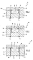
- the reference 10 generally denotes the component of the invention, which comprises a substrate 12, in particular a substrate made of silicon or other semiconductor or quartz material, incorporating an active element such as a sensor 14.
- This sensor can be for example a blood pressure sensor (SAW type or BAW) or an accelerometer (piezoelectric or MEMS-based) intended in particular to measure the endocardial acceleration (EA) at the end of a probe implanted in the body. apex of the ventricle.
- the thickness of the substrate 12 can be reduced by breaking-in at a very low value, up to about 200 .mu.m, making it possible to have a component of very small thickness that is easy to integrate into implanted probes of very small dimensions.
- the electrical connection to the sensor 14 is achieved by conductive pads 16 exposed outside the component and coated with a deposit ensuring the biocompatibility, for example a gold deposit.
- These contact pads 16 are located on one face of the substrate 12 opposite to the face where the sensor 14 is integrated, and the connection to the conductor 18 in contact with the sensor 14 is provided via vias 20, for example made by plasma etching through the substrate 12 and then filled by electrolytic deposition of copper or any other suitable metal; such a technology is described for example in the US 2004/0259325 A1 , which can be referred to for more details.
- the substrate 12 is closed, on the side where the sensor 14 is located, by a cover 22, also made of silicon or quartz, which, in the example illustrated in FIG. 1, has a recess 24 reserved on the internal side facing the sensor.
- the substrate 12 and the cover 22 are directly sealed to each other by their faces facing each other, at the interface 26.
- Such a silicon-direct sealing technique on-silicon is described for example in the US 6,979,597 A1 , which can be referred to for further details.
- the substrate 12 and the cover 22 are not sealed directly to one another, but via an intermediate sealing ring 28, for example a metal or alloy ring.
- an intermediate sealing ring 28 for example a metal or alloy ring.
- biocompatible metal in particular based on gold or palladium; this technology is for example described in the US-A-6,118,181 which can be referred to for further details.
- the material of the sealing ring can also be a suitable glass with low levels of impurities.
- this silicon is advantageously doped with boron, this doping having the property of improving its biocompatibility, as described in particular in FIG. US-A-6,968,743 .
- the pads 16 forming contact electrodes are extended and configured in a suitable pattern 30 so as to form an antenna (dipole, loop, ...) for providing a non-galvanic connection with the sensor 14.
- the latter can then be remotely powered and incorporated into a completely autonomous component, without a wired connection.
- a component provided with RF communication functions may notably constitute an implantable radio frequency identification device (RFID) operating in frequency bands such as the 402-405 MHz Medical Implants Communication System (MICS) band or the ISM public unmarked bands.
- RFID radio frequency identification device
- MIMS Medical Implants Communication System
- ISM ISM public unmarked bands.
- Industrial, Scientific and Medical 863-870 MHz, 902-928 MHz and 2.4 GHz used by medical devices, allowing interrogation of the active element 14 remotely by an "RF telemetry" technique.
- FIG. 4 illustrates the different steps of a Thin Film Packaging (TFP) type process applied to the production of a component according to the invention.
- TFP Thin Film Packaging
- the sensor is then protected by a thin cover made directly on the substrate by deposition and etching steps, in place of a sealed cover, as in the case of the embodiments illustrated in FIGS. 1 to 3.
- the first step (step a) consists in producing the sensor 14 on the substrate 12.
- a first sacrificial layer 32 is deposited locally near, but remotely, the sensor 14.
- step c Another sacrificial layer 34, of great thickness, is then deposited (step c), which encompasses the sensor 14, to the place of the first sacrificial layer 32.
- step d consists in depositing a film or thin layer of closure 36, which will subsequently constitute the lid of the component on the assembly thus formed.
- An opening 38 is formed in this layer 36 in line with the first sacrificial layer 32.
- suitable materials may be employed which provide a hermeticity at the desired degree, for example nitride film deposits by technique PECVD.
- step e consists in eliminating the two sacrificial layers 32 and 34 by etching through the opening 38. This allows the formation around the sensor 14 of a free internal volume 40 closed by the layer 36 to exception of opening 38.
- This opening 38 is then closed (step f) by a dielectric deposit 42 to ensure the hermeticity of the internal volume 40.
- the final step (step g) consists in producing on the periphery of the volume 40 surrounding the sensor 14 the openings 44 for access to the contacts (not shown) for electrical connection to this sensor. Note that in this embodiment the contacts are taken on the same side of the substrate 12 as that incorporating the sensor 14, unlike Figures 1 to 3 where the contacts were taken on the opposite side.
- FIG. 5 shows, in plan, an example of a component 10 according to the invention, glued on a support 46 such as a flexible or flexible circuit.
- This support 46 carries connecting surfaces 48 connected to pads or "pads” via interconnections 52 deposited on the substrate.
- the pads 50 are located in the vicinity, and opposite, homologous contact pads 16 of the circuit 10, to which they are connected by "bonding" wires 54.
- each contact pad 16 of the circuit is electrically connected to one of the surfaces 48, on which may be welded the end of a microcable 56 connecting to a remote device.
Landscapes
- Engineering & Computer Science (AREA)
- Microelectronics & Electronic Packaging (AREA)
- Computer Hardware Design (AREA)
- Electrotherapy Devices (AREA)
- Measuring And Recording Apparatus For Diagnosis (AREA)
- Measurement And Recording Of Electrical Phenomena And Electrical Characteristics Of The Living Body (AREA)
Abstract
Description
- L'invention concerne, de façon générale, le domaine des "dispositifs médicaux actifs" tels que définis par la directive 93/42/CE du 14 juin 1993 du Conseil des communautés européennes, et notamment les "dispositifs médicaux implantables actifs" tels que définis par la directive du Conseil 90/385/CEE du 20 juin 1990.
- Cette définition inclut en particulier les appareils chargés de surveiller l'activité cardiaque et de générer des impulsions de stimulation, de resynchronisation, de défibrillation et/ou de cardioversion en cas de trouble du rythme détecté par l'appareil. Elle inclut aussi les appareils neurologiques, les pompes de diffusion de substances médicales, les implants cochléaires, les capteurs biologiques implantés, etc., ainsi que les dispositifs de mesure de pH ou encore d'impédance intracorporelle (telle que mesure d'impédance transpulmonaire ou d'impédance intracardiaque).
- Les dispositifs médicaux implantables actifs font appel, pour le recueil des signaux et le pilotage des diverses fonctions, à des capteurs qui peuvent être notamment intégrés à une sonde elle-même reliée à un boîtier de générateur du dispositif. Des exemples typiques de tels capteurs sont les capteurs de pression sanguine ou d'accélération endocardiaque (EA) montés à l'extrémité distale d'une sonde endocavitaire introduite dans le myocarde et reliée au boîtier d'un stimulateur ou défibrillateur.
- L'invention concerne plus précisément un composant biocompatible implantable dans le corps humain, qui incorpore un élément actif encapsulé de manière hermétique tel qu'un capteur de mesure d'un paramètre physiologique, un microsystème électromécanique ou un circuit électronique intégré
- Par commodité, cet élément actif sera désigné par la suite simplement "capteur", mais l'invention ne doit pas être entendue de manière limitative et on comprendra qu'elle couvre non seulement les capteurs proprement dits, c'est-à-dire les transducteurs de signal permettant de produire un signal électrique fonction des variations d'un paramètre physique, mais également les circuits électroniques actifs tels qu'amplificateurs, filtres, ... associés ou non à un capteur pour être disposés à proximité de ce dernier, ou encore les microsystèmes électromécaniques (MEMS), et de façon générale tout élément technologiquement intégrable sur un substrat en un matériau tel que le silicium ou autre matériau semiconducteur.
- Les capteurs implantés sont soumis à des exigences très strictes, en particulier lorsqu'ils sont en contact avec le sang ou d'autres fluides corporels, surtout lorsque ce contact est permanent, sur une durée pouvant atteindre plusieurs années dans le cas des implants cardiaques.
- Ces exigences, qui sont notamment développées dans la norme ISO 10993, sont de deux ordres :
- biocompatibilité des matériaux employés, c'est-à-dire que ces matériaux doivent rester totalement inertes à l'égard des tissus et fluides corporels environnants (innocuité) et, inversement, ces tissus ou fluides ne doivent entraîner aucune corrosion ou dégradation des propriétés des matériaux, qui doivent rester intacts en dépit du contact prolongé avec le milieu biologique environnant.
- herméticité, c'est-à-dire que le capteur doit être résistant non seulement à la pénétration des liquides (étanchéité), mais également à celle des gaz, ce qui suppose un taux de fuite parfaitement contrôlé et infinitésimal.
- Longtemps, il a suffi d'enrober le capteur dans un matériau biocompatible, mais certaines normes plus récentes exigent dorénavant un double niveau de protection, avec une biocompatibilité non seulement au niveau de l'enrobage, mais également pour l'élément situé sous celui-ci. Il s'agit d'assurer la protection même en cas de contact indirect, par exemple du fait d'une diffusion au travers de l'enrobage entre le capteur et le milieu environnant, ou encore en cas de dégradation, blessure, fissuration, ... de l'enrobage après une période prolongée.
- Pour répondre à ces exigences très strictes, la solution actuelle consiste à incorporer le capteur dans un boîtier en métal inerte, généralement en titane. Des traversées en céramique soudées sur le boîtier permettent d'établir les liaisons électriques entre le capteur enfermé dans le boîtier et l'extérieur afin d'établir la connexion aux conducteurs internes de la sonde.
- Cette solution répond parfaitement aux exigences de biocompatibilité et d'herméticité exposées plus haut.
- En revanche, elle est coûteuse, en raison de la technologie délicate à mettre en oeuvre, du recours à des composants coûteux et difficiles à assembler, et à l'impossibilité d'un traitement automatisé, à plus forte raison d'un traitement collectif, qui permettrait une production en série.
- De plus, cette technique conduit à des composants relativement volumineux, en raison du recours à un boîtier qui ne peut pas être miniaturisé autant que cela serait souhaitable. Or il existe un besoin de capteurs de très faibles dimensions qui puissent être notamment placés sur des sondes de faible diamètre, compatibles avec une mise en place par les techniques habituelles de cathéterisation du réseau veineux.
- Le but de l'invention est de proposer un composant incluant un capteur (ou autre élément actif) évitant le recours à un boîtier titane et à des traversées pour la liaison électrique, qui puisse néanmoins assurer parfaitement une biocompatibilité et une herméticité au degré requis par les contraintes très strictes résultant du caractère implantable de ce composant et de la nécessité de résister à un contact prolongé avec les tissus et fluides corporels tels que le sang.
- L'invention a notamment pour but de garantir ces performances de biocompatibilité et d'herméticité sur une très longue durée, typiquement de plusieurs années dans le cas des implants cardiaques.
- Un autre but de l'invention est de permettre un abaissement des coûts de fabrication d'un tel composant, par mise en oeuvre de technologies par ailleurs éprouvées, en offrant également une possibilité de fabrication par traitement collectif.
- Un autre but encore de l'invention est de proposer un tel composant présentant une miniaturisation poussée, permettant notamment de placer un ou plusieurs de ces composants sur des sondes de faible diamètre.
- Un autre but encore de l'invention est de proposer un composant de ce type dont la configuration permette sa téléalimentation et l'échange de données par voie non galvanique, typiquement par une liaison RF, sans accroissement indu de la complexité technologique.
- Le
US 4 023 562 A1 décrit un capteur de pression intégré dans un substrat, encapsulé sous un couvercle permettant d'obtenir un ensemble dont la biocompatibilité permet par exemple de l'introduire dans un cathéter lors d'une intervention pour mesurer une pression en un emplacement donné du corps humain. - La configuration décrite par ce document n'est toutefois pas adaptée aux buts énoncés ci-dessus : notamment, elle ne procure pas de biocompatibilité et d'herméticité sur une très longue durée, et n'offre pas la possibilité d'une fabrication collective.
- En effet, dans ce document, la prise de contact avec les bornes du capteur se fait par des plages métallisées disposées sur le côté du couvercle, dans le même plan que le composant ; la liaison électrique est réalisée par une tranchée horizontale, formée également dans ce plan, avec une diffusion au bore pour la rendre conductrice. Cette technique ne permet pas d'obtenir des contacts de faible résistance, car la résistivité d'une diffusion au bore est notablement supérieure à celle d'un métal. Au surplus, la technique proposée ne permet pas un traitement collectif des plaquettes d'une même tranche de silicium, dans la mesure où il n'est pas possible de scier simultanément le substrat de base et le capot en raison de la prise de contact latérale.
- Au surplus, le silicium du substrat et du capot est dopé au phosphore, ce qui ne lui confère pas de biocompatibilité à long terme, et rend ce composant utilisable seulement pour des interventions de relativement courte durée (quelques heures, tout au plus quelques jours).
- Le
US 2003/0209357 A1 décrit une technique consistant à reporter un composant sur un substrat, puis à encapsuler le tout avec un capot de silicium. La prise de contact est opérée par la face opposée du substrat sur lequel est rapporté le composant MEMS. Pour cela, le substrat est creusé largement par attaque au KOH, de part en part, jusqu'à une métallisation présente sur la face opposée ; la liaison électrique est obtenue en tapissant la paroi de ces trous d'une métallisation. - Du fait notamment des trous traversants de grande dimension, le composant obtenu n'est pas susceptible de procurer l'herméticité nécessaire à un implant corporel (ce n'est d'ailleurs pas l'application visée par ce document).
- Au surplus, la nécessité de reporter un composant sur le substrat, outre l'augmentation de taille, ne permet pas de traitement collectif susceptible d'abaisser le coût de fabrication.
- Pour atteindre les buts énoncés ci-dessus, l'invention propose un composant du type général divulgué par le
US4 023 562 A1 précité, correspondant au préambule de la revendication 1, et comprenant en outre les caractéristiques additionnelles énoncées dans la partie caractérisante de cette revendication 1, de manière à le rendre biocompatible et implantable dans le corps humain. Les sous-revendications visent des formes de réalisation subsidiaires avantageuses. - On va maintenant décrire un exemple de mise en oeuvre du dispositif de l'invention, en référence aux dessins annexés où les mêmes références numériques désignent d'une figure à l'autre des éléments identiques ou fonctionnellement semblables.
- La figure 1 est une vue en coupe schématique d'un composant selon l'invention, où substrat et boîtier sont directement scellés l'un à l'autre.
- La figure 2 est une variante de la figure 1, où substrat et couvercle sont soudés avec interposition d'un anneau de scellement approprié.
- La figure 3 illustre une variante de la figure 2, adaptée à la réalisation d'un composant pourvu de fonctions RF.
- La figure 4 illustre les différentes étapes d'un procédé de type "Thin Film Packaging" (TFP) pour la réalisation d'un composant selon les enseignements de l'invention.
- La figure 5 est une vue en plan du composant de l'invention, monté sur un support avec sa connectique adaptée.
- On va maintenant décrire un exemple de réalisation du composant de l'invention.
- Sur les figures, la référence 10 désigne de façon générale le composant de l'invention, qui comprend un substrat 12, notamment un substrat en silicium ou autre matériau semiconducteur ou en quartz, intégrant un élément actif tel qu'un capteur 14. Ce capteur peut être par exemple un capteur de pression sanguine (de type SAW ou BAW) ou un accéléromètre (piézoélectrique ou à base de MEMS) destiné en particulier à mesurer l'accélération endocardiaque (EA) à l'extrémité d'une sonde implantée dans l'apex du ventricule.
- L'épaisseur du substrat 12 peut être réduite par rodage à une valeur très faible, jusqu'à 200µm environ, permettant de disposer d'un composant de très faible épaisseur, aisé à intégrer dans des sondes implantées de très faibles dimensions.
- La liaison électrique au capteur 14 est réalisée par des plages conductrices 16 apparentes à l'extérieur du composant et revêtues d'un dépôt assurant la biocompatibilité, par exemple un dépôt d'or. Ces plages de contact 16 sont situées sur une face du substrat 12 opposée à la face où est intégré le capteur 14, et la liaison au conducteur 18 en contact avec le capteur 14 est assurée par l'intermédiaire de vias 20, par exemple réalisées par gravure plasma au travers du substrat 12 puis remplis par dépôt électrolytique de cuivre ou tout autre métal approprié ; une telle technologie est décrite par exemple dans le
US 2004/0259325 A1 , auquel on pourra se référer pour plus de détails. - Le substrat 12 est fermé, du côté où est situé le capteur 14, par un couvercle 22, également en silicium ou quartz, qui, dans l'exemple illustré figure 1, comporte un évidement 24 réservé côté interne, face au capteur.
- Dans l'exemple de la figure 1, le substrat 12 et le couvercle 22 sont directement scellés l'un à l'autre par leurs faces en vis-à-vis, à l'interface 26. Une telle technique de scellement direct silicium-sur-silicium est décrite par exemple dans le
US 6 979 597 A1 , auquel on pourra se référer pour de plus amples détails. - Cette technique de réalisation des prises de contact présente plusieurs avantages majeurs :
- elle permet de réaliser des contacts de très faible résistance, grâce au remplissage par un métal ;
- ce remplissage de métal permet d'assurer une excellente herméticité entre le volume intérieur et la cavité 24 où se situe le capteur 14, et la face opposée où se trouvent les plages de contact 16,
- enfin, cette configuration est parfaitement compatible avec un traitement collectif, le substrat 12 et le couvercle 22 pouvant être sciés ensemble de manière à individualiser le composant 10.
- Dans la variante de la figure 2, le substrat 12 et le couvercle 22 ne sont pas scellés directement l'un à l'autre, mais par l'intermédiaire d'un anneau de scellement intercalaire 28, par exemple un anneau en métal ou alliage métallique biocompatible, notamment à base d'or ou de palladium ; cette technologie est par exemple décrite dans le
US-A-6 118 181 auquel on pourra se référer pour de plus amples détails. Le matériau de l'anneau de scellement peut être également un verre approprié, à faible taux d'impuretés. - Lorsque du silicium est utilisé comme matériau pour le substrat 12 et le couvercle 22, ce silicium est avantageusement dopé au bore, ce dopage ayant la propriété d'améliorer sa biocompatibilité, comme décrit notamment dans le
US-A-6 968 743 . - Dans la variante de la figure 3, les plages 16 formant électrodes de contact sont prolongées et configurées suivant un motif approprié 30 de manière à former une antenne (dipôle, boucle, ...) permettant d'assurer une liaison non galvanique avec le capteur 14. Ce dernier peut alors être téléalimenté et incorporé à un composant totalement autonome, dépourvu de liaison filaire. Un tel composant pourvu de fonctions de communication RF peut notamment constituer un dispositif d'identification radiofréquence (RFID) implantable, opérant dans des bandes de fréquences telles que la bande MICS (Medical Implants Communication System) 402-405 MHz ou les bandes banalisées publiques ISM (Industriel, Scientifique et Médical) 863-870 MHz, 902-928 MHz et 2,4 GHz utilisées par les dispositifs médicaux, autorisant l'interrogation de l'élément actif 14 à distance par une technique de "télémétrie RF".
- La figure 4 illustre les différentes étapes d'un procédé de type "Thin Film Packaging" (TFP) appliqué à la réalisation d'un composant selon l'invention.
- Le capteur est alors protégé par un capot mince réalisé directement sur le substrat par des étapes de dépôt et de gravure, en lieu et place d'un capot rapporté scellé, comme dans le cas des modes de réalisation illustrés figures 1 à 3.
- La première étape (étape a) consiste à réaliser le capteur 14 sur le substrat 12.
- Ensuite (étape b), une première couche sacrificielle 32, de faible épaisseur, est déposée localement à proximité, mais à distance, du capteur 14.
- Une autre couche sacrificielle 34, de forte épaisseur, est ensuite déposée (étape c), qui vient englober le capteur 14, jusqu'à l'endroit de la première couche sacrificielle 32.
- L'étape suivante (étape d) consiste à déposer un film ou couche mince de fermeture 36, qui constituera ultérieurement le couvercle du composant sur l'ensemble ainsi formé. Une ouverture 38 est pratiquée dans cette couche 36 au droit de la première couche sacrificielle 32. Pour la réalisation du capot mince 36, divers matériaux appropriés peuvent être employés qui assurent une herméticité au degré souhaité, par exemple des dépôts de film de nitrure par technique PECVD.
- L'étape suivante (étape e) consiste à éliminer les deux couches sacrificielles 32 et 34 par attaque au travers de l'ouverture 38. Ceci permet la formation autour du capteur 14 d'un volume interne libre 40 clos par la couche 36 à l'exception de l'ouverture 38.
- Cette ouverture 38 est ensuite obturée (étape f) par un dépôt diélectrique 42 permettant d'assurer l'herméticité du volume intérieur 40.
- L'étape finale (étape g) consiste à réaliser à la périphérie du volume 40 entourant le capteur 14 les ouvertures 44 d'accès aux contacts (non représentés) de liaison électrique à ce capteur. On notera que dans ce mode de réalisation les contacts sont pris sur la même face du substrat 12 que celle intégrant le capteur 14, à la différence des figures 1 à 3 où les contacts étaient pris sur la face opposée.
- La figure 5 montre, en plan, un exemple d'un composant 10 selon l'invention, collé sur un support 46 tel qu'un circuit souple ou flexible. Ce support 46 porte des surfaces de liaison 48 reliées à des plages ou "pads" via des interconnexions 52 déposées sur le substrat. Les plages 50 sont situées à proximité, et en vis-à-vis, des plages de contact homologues 16 du circuit 10, auxquelles elles sont reliées par des fils de "bonding" 54. De cette manière, chaque plage de contact 16 du circuit est électriquement reliée à l'une des surfaces 48, sur laquelle pourra être soudée l'extrémité d'un microcâble 56 de liaison à un dispositif distant.
Claims (9)
- Un composant biocompatible implantable dans le corps humain incorporant, encapsulé de manière hermétique, un élément de type capteur de mesure d'un paramètre physiologique, microsystème électromécanique ou circuit électronique, ce composant (10) comprenant :- un substrat de base (12) en silicium ou quartz ayant sur l'une de ses faces l'élément (14), et pourvu de plages métalliques (16), biocompatibles avec l'environnement extérieur, formées sur une surface libre de ce même substrat (16), ces plages étant électriquement reliées à l'élément par des liaisons électriques (20) intégrées au substrat ; et- un couvercle (22) en silicium ou quartz recouvrant et fermant périphériquement le substrat de manière hermétique, du côté de la face intégrant l'élément,ce composant étant essentiellement dépourvu de boîtier métallique d'isolement de l'élément d'avec l'environnement extérieur, et de traversées isolantes rapportées pour la liaison électrique à l'élément,
caractérisé en ce que :- ledit élément (14) est un élément actif intégré audit substrat (12) ;- lesdites plages métalliques (16) sont situées sur une face du substrat opposée à la face où est situé ledit élément actif intégré (14) ; et- le substrat comprend des vias (20) de liaison desdites plages métalliques (16) à des conducteurs (18) en contact avec ledit élément actif intégré (14), ces vias étant des vias gravés au travers du substrat (12) et remplis d'un métal. - Le composant biocompatible implantable de la revendication 1, dans lequel lesdites plages métalliques (16) sont des plages revêtues d'or.
- Le composant biocompatible implantable de la revendication 1, dans lequel l'élément actif intégré (14) comprend des circuits radiofréquence et/ou téléalimentés, et dans lequel au moins certaines des plages métalliques (16) sont des plages dont les dimensions et la configuration respective sont choisies de manière à former une antenne (30).
- Le composant biocompatible implantable de la revendication 1, dans lequel le matériau du substrat (12) et du couvercle (22) est un silicium dopé au bore.
- Le composant biocompatible implantable de la revendication 1, dans lequel substrat (12) et couvercle (22) sont directement scellés l'un à l'autre par leurs faces en vis-à-vis.
- Le composant biocompatible implantable de la revendication 1, dans lequel substrat (12) et couvercle (22)) sont soudés l'un à l'autre avec interposition entre leurs faces en vis-à-vis d'un anneau de scellement (28) en matériau biocompatible avec l'environnement extérieur.
- Le composant biocompatible implantable de la revendication 6, dans lequel le matériau de l'anneau de scellement (28) est un verre.
- Le composant biocompatible implantable de la revendication 6, dans lequel le matériau de l'anneau de scellement (28) est un métal ou un alliage métallique biocompatibles, notamment or ou palladium.
- Le composant biocompatible implantable de la revendication 1, dans lequel le couvercle (22) est un capot mince (36) réalisé par une technique de type Thin Film Packaging TFP.
Applications Claiming Priority (1)
| Application Number | Priority Date | Filing Date | Title |
|---|---|---|---|
| FR0608369 | 2006-09-25 |
Publications (3)
| Publication Number | Publication Date |
|---|---|
| EP1903000A2 true EP1903000A2 (fr) | 2008-03-26 |
| EP1903000A3 EP1903000A3 (fr) | 2012-07-04 |
| EP1903000B1 EP1903000B1 (fr) | 2019-09-18 |
Family
ID=37992717
Family Applications (1)
| Application Number | Title | Priority Date | Filing Date |
|---|---|---|---|
| EP07291120.9A Active EP1903000B1 (fr) | 2006-09-25 | 2007-09-21 | Composant biocompatible implantable incorporant un élément actif intégré tel qu'un capteur de mesure d'un paramètre physiologique, microsystème électromécanique ou circuit électronique |
Country Status (3)
| Country | Link |
|---|---|
| US (1) | US9126825B2 (fr) |
| EP (1) | EP1903000B1 (fr) |
| JP (1) | JP5258245B2 (fr) |
Cited By (2)
| Publication number | Priority date | Publication date | Assignee | Title |
|---|---|---|---|---|
| EP2660190A1 (fr) | 2012-05-03 | 2013-11-06 | Commissariat à l'Énergie Atomique et aux Énergies Alternatives | Composant à élément actif encapsulé et dispositif médical implantable comportant un tel composant |
| CN110352082A (zh) * | 2016-12-30 | 2019-10-18 | 索林Crm联合股份公司 | 用于心脏刺激的自主可植入胶囊 |
Families Citing this family (71)
| Publication number | Priority date | Publication date | Assignee | Title |
|---|---|---|---|---|
| KR101260981B1 (ko) | 2004-06-04 | 2013-05-10 | 더 보오드 오브 트러스티스 오브 더 유니버시티 오브 일리노이즈 | 인쇄가능한 반도체소자들의 제조 및 조립방법과 장치 |
| US8372726B2 (en) | 2008-10-07 | 2013-02-12 | Mc10, Inc. | Methods and applications of non-planar imaging arrays |
| US8097926B2 (en) | 2008-10-07 | 2012-01-17 | Mc10, Inc. | Systems, methods, and devices having stretchable integrated circuitry for sensing and delivering therapy |
| US8886334B2 (en) | 2008-10-07 | 2014-11-11 | Mc10, Inc. | Systems, methods, and devices using stretchable or flexible electronics for medical applications |
| US8389862B2 (en) | 2008-10-07 | 2013-03-05 | Mc10, Inc. | Extremely stretchable electronics |
| JP5646492B2 (ja) | 2008-10-07 | 2014-12-24 | エムシー10 インコーポレイテッドMc10,Inc. | 伸縮可能な集積回路およびセンサアレイを有する装置 |
| GB0820629D0 (en) * | 2008-11-11 | 2008-12-17 | Univ Bath | Biocompatible electrode |
| US8072056B2 (en) | 2009-06-10 | 2011-12-06 | Medtronic, Inc. | Apparatus for restricting moisture ingress |
| EP2302327B1 (fr) * | 2009-09-25 | 2020-02-26 | Nxp B.V. | Capteur |
| WO2011041727A1 (fr) | 2009-10-01 | 2011-04-07 | Mc10, Inc. | Boîtiers protecteurs avec des circuits électroniques intégrés |
| WO2011115643A1 (fr) | 2010-03-17 | 2011-09-22 | The Board Of Trustees Of The University Of Illinois | Dispositifs biomédicaux implantables sur substrats biorésorbables |
| EP2513953B1 (fr) | 2009-12-16 | 2017-10-18 | The Board of Trustees of the University of Illionis | Électrophysiologie faisant intervenir des équipements électroniques conformes |
| US10441185B2 (en) | 2009-12-16 | 2019-10-15 | The Board Of Trustees Of The University Of Illinois | Flexible and stretchable electronic systems for epidermal electronics |
| US9936574B2 (en) | 2009-12-16 | 2018-04-03 | The Board Of Trustees Of The University Of Illinois | Waterproof stretchable optoelectronics |
| US20110249381A1 (en) * | 2010-04-13 | 2011-10-13 | Michael Diebold | Mini implant |
| US10852069B2 (en) | 2010-05-04 | 2020-12-01 | Fractal Heatsink Technologies, LLC | System and method for maintaining efficiency of a fractal heat sink |
| US20130223028A1 (en) * | 2010-07-29 | 2013-08-29 | Proteus Digital Health, Inc. | Hybrid housing for implantable medical device |
| US9171721B2 (en) | 2010-10-26 | 2015-10-27 | Medtronic, Inc. | Laser assisted direct bonding |
| US8666505B2 (en) | 2010-10-26 | 2014-03-04 | Medtronic, Inc. | Wafer-scale package including power source |
| US8796109B2 (en) | 2010-12-23 | 2014-08-05 | Medtronic, Inc. | Techniques for bonding substrates using an intermediate layer |
| US12115374B2 (en) | 2011-01-28 | 2024-10-15 | Curonix Llc | Microwave field stimulator |
| EP4424360A3 (fr) | 2011-01-28 | 2025-01-22 | Curonix LLC | Système de stimulateur neuronal |
| US8424388B2 (en) | 2011-01-28 | 2013-04-23 | Medtronic, Inc. | Implantable capacitive pressure sensor apparatus and methods regarding same |
| US9220897B2 (en) | 2011-04-04 | 2015-12-29 | Micron Devices Llc | Implantable lead |
| MX346885B (es) * | 2011-04-04 | 2017-04-04 | Stimwave Tech Inc | Conductor implantable. |
| US9765934B2 (en) | 2011-05-16 | 2017-09-19 | The Board Of Trustees Of The University Of Illinois | Thermally managed LED arrays assembled by printing |
| KR102000302B1 (ko) | 2011-05-27 | 2019-07-15 | 엠씨10, 인크 | 전자, 광학, 및/또는 기계 장치 및 시스템, 그리고 이를 제조하기 위한 방법 |
| US8934965B2 (en) | 2011-06-03 | 2015-01-13 | The Board Of Trustees Of The University Of Illinois | Conformable actively multiplexed high-density surface electrode array for brain interfacing |
| CN104080509B (zh) | 2011-07-29 | 2017-09-08 | 米克伦设备有限责任公司 | 用于神经刺激器的功率或极性选择的远程控制 |
| EP2741810B1 (fr) | 2011-08-12 | 2021-03-31 | Stimwave Technologies Incorporated | Stimulateur de champs hyperfréquences |
| EP3403690B1 (fr) | 2011-09-15 | 2020-08-05 | Stimwave Technologies Incorporated | Module de relais pour implant |
| WO2013089867A2 (fr) | 2011-12-01 | 2013-06-20 | The Board Of Trustees Of The University Of Illinois | Dispositifs transitoires conçus pour subir des transformations programmables |
| US9554484B2 (en) | 2012-03-30 | 2017-01-24 | The Board Of Trustees Of The University Of Illinois | Appendage mountable electronic devices conformable to surfaces |
| US20150250386A1 (en) | 2012-09-28 | 2015-09-10 | Csem Centre Suisse D'electronique Et De Microtechnique Sa -Recherche Et Developpement | Implantable devices |
| US9171794B2 (en) | 2012-10-09 | 2015-10-27 | Mc10, Inc. | Embedding thin chips in polymer |
| JP6435272B2 (ja) * | 2012-12-21 | 2018-12-05 | マイクロチップス バイオテック,インコーポレイテッド | 低侵襲挿入のための植え込み型医療デバイス |
| WO2014105973A1 (fr) | 2012-12-26 | 2014-07-03 | Micron Devices, LLC | Ensemble antenne portable |
| US8874182B2 (en) * | 2013-01-15 | 2014-10-28 | Google Inc. | Encapsulated electronics |
| US9884197B2 (en) * | 2013-07-01 | 2018-02-06 | Newsouth Innovations Pty Ltd | Encapsulated electronic circuit |
| CN110665114B (zh) | 2014-05-12 | 2022-12-06 | 斯蒂维科技公司 | 具有小尺寸发射天线的远程rf功率系统 |
| US9968794B2 (en) | 2014-12-24 | 2018-05-15 | Medtronic, Inc. | Implantable medical device system including feedthrough assembly and method of forming same |
| US9865533B2 (en) | 2014-12-24 | 2018-01-09 | Medtronic, Inc. | Feedthrough assemblies |
| US10124559B2 (en) | 2014-12-24 | 2018-11-13 | Medtronic, Inc. | Kinetically limited nano-scale diffusion bond structures and methods |
| US10136535B2 (en) | 2014-12-24 | 2018-11-20 | Medtronic, Inc. | Hermetically-sealed packages including feedthrough assemblies |
| BR112017025609A2 (pt) | 2015-06-01 | 2018-08-07 | The Board Of Trustees Of The University Of Illinois | sistemas eletrônicos miniaturizados com potência sem fio e capacidades de comunicação de campo próximo |
| BR112017025616A2 (en) | 2015-06-01 | 2018-08-07 | The Board Of Trustees Of The University Of Illinois | alternative approach to uv capture |
| US10925543B2 (en) | 2015-11-11 | 2021-02-23 | The Board Of Trustees Of The University Of Illinois | Bioresorbable silicon electronics for transient implants |
| US10098589B2 (en) | 2015-12-21 | 2018-10-16 | Medtronic, Inc. | Sealed package and method of forming same |
| JP6622149B2 (ja) * | 2016-06-28 | 2019-12-18 | 日本電信電話株式会社 | ウェアラブルデバイス |
| US10130302B2 (en) * | 2016-06-29 | 2018-11-20 | International Business Machines Corporation | Via and trench filling using injection molded soldering |
| WO2019074950A1 (fr) * | 2017-10-10 | 2019-04-18 | Massachusetts Institute Of Technology | Procédé d'atténuation neuromécanique et neuroélectromagnétique d'une pathologie de membre |
| WO2019152870A1 (fr) | 2018-02-01 | 2019-08-08 | Perryman Laura Tyler | Systèmes et procédés permettant de détecter une impédance électrode de stimulation-tissu |
| CN112566548A (zh) * | 2018-03-20 | 2021-03-26 | 格拉夫威尔科技公司 | 可替换式传感器系统和方法 |
| DE102018208538A1 (de) | 2018-05-30 | 2019-12-05 | Kardion Gmbh | Intravasale Blutpumpe und Verfahren zur Herstellung von elektrischen Leiterbahnen |
| DE102018208933A1 (de) | 2018-06-06 | 2019-12-12 | Kardion Gmbh | Verfahren zur Bestimmung einer Strömungsgeschwindigkeit eines durch ein implantiertes, vaskuläres Unterstützungssystem strömenden Fluids |
| DE102018208916A1 (de) * | 2018-06-06 | 2019-12-12 | Kardion Gmbh | Sensorikeinheit für ein Implantationssystem zur medizinischen Unterstützung eines Patienten und Verfahren zum Herstellen einer Sensorikeinheit |
| DE102018208913A1 (de) | 2018-06-06 | 2019-12-12 | Kardion Gmbh | Verfahren zum Betreiben eines implantierten, ventrikulären Unterstützungssystems |
| DE102018208931A1 (de) | 2018-06-06 | 2019-12-12 | Kardion Gmbh | Vorrichtung zum Bestimmen eines Herzzeitvolumens für ein Herzunterstützungssystem, Herzunterstützungssystem und Verfahren zum Bestimmen eines Herzzeitvolumens |
| DE102018208945A1 (de) | 2018-06-06 | 2019-12-12 | Kardion Gmbh | Analysevorrichtung und Verfahren zum Analysieren einer Viskosität eines Fluids |
| DE102018208870A1 (de) | 2018-06-06 | 2019-12-12 | Kardion Gmbh | Verfahren zur Bestimmung eines Fluid-Volumenstroms durch ein implantiertes, vaskuläres Unterstützungssystem |
| DE102018208899A1 (de) | 2018-06-06 | 2019-12-12 | Kardion Gmbh | Verfahren zum Ermitteln der Schallgeschwindigkeit in einem Fluid im Bereich eines implantierten, vaskulären Unterstützungssystems |
| DE102018208892A1 (de) | 2018-06-06 | 2019-12-12 | Kardion Gmbh | Sensorkopfvorrichtung für ein minimalinvasives Herzunterstützungssystem und Verfahren zum Herstellen einer Sensorkopfvorrichtung für ein Herzunterstützungssystem |
| DE102018208862A1 (de) | 2018-06-06 | 2019-12-12 | Kardion Gmbh | Implantierbares, vaskuläres Unterstützungssystem |
| DE102018208936A1 (de) | 2018-06-06 | 2019-12-12 | Kardion Gmbh | Bestimmvorrichtung und Verfahren zum Bestimmen einer Viskosität eines Fluids |
| DE102018208929A1 (de) | 2018-06-06 | 2019-12-12 | Kardion Gmbh | Verfahren zur Bestimmung einer Strömungsgeschwindigkeit eines durch ein implantiertes, vaskuläres Unterstützungssystem strömenden Fluids |
| DE102018208879A1 (de) | 2018-06-06 | 2020-01-30 | Kardion Gmbh | Verfahren zur Bestimmung eines Fluid-Gesamtvolumenstroms im Bereich eines implantierten, vaskuläres Unterstützungssystems |
| DE102018210076A1 (de) | 2018-06-21 | 2019-12-24 | Kardion Gmbh | Verfahren und Vorrichtung zum Erkennen eines Verschleißzustands eines Herzunterstützungssystems, Verfahren und Vorrichtung zum Betreiben eines Herzunterstützungssystems und Herzunterstützungssystem |
| DE102018213350A1 (de) | 2018-08-08 | 2020-02-13 | Kardion Gmbh | Vorrichtung und Verfahren zur Überwachung eines Gesundheitszustands des Patienten |
| JP7028755B2 (ja) * | 2018-11-27 | 2022-03-02 | ショット日本株式会社 | 生体適合性貫通電極付きガラス基板ならびに生体適合性小型電子デバイス |
| WO2021034784A1 (fr) | 2019-08-16 | 2021-02-25 | Poltorak Technologies, LLC | Dispositif et procédé de diagnostic médical |
| US12502524B2 (en) | 2021-12-03 | 2025-12-23 | Kardion Gmbh | Cardiac pump with optical fiber for laser doppler |
Family Cites Families (23)
| Publication number | Priority date | Publication date | Assignee | Title |
|---|---|---|---|---|
| US4023562A (en) * | 1975-09-02 | 1977-05-17 | Case Western Reserve University | Miniature pressure transducer for medical use and assembly method |
| IT1245814B (it) * | 1991-05-21 | 1994-10-18 | Sorin Biomedica Spa | Dispositivo cardiostimolatore del tipo rate responsive |
| US6120460A (en) * | 1996-09-04 | 2000-09-19 | Abreu; Marcio Marc | Method and apparatus for signal acquisition, processing and transmission for evaluation of bodily functions |
| US6544193B2 (en) * | 1996-09-04 | 2003-04-08 | Marcio Marc Abreu | Noninvasive measurement of chemical substances |
| US6118181A (en) * | 1998-07-29 | 2000-09-12 | Agilent Technologies, Inc. | System and method for bonding wafers |
| CN100385232C (zh) * | 1998-08-26 | 2008-04-30 | 医药及科学传感器公司 | 基于光学的感测装置 |
| JP2000325320A (ja) * | 1999-05-18 | 2000-11-28 | Tdk Corp | 生体内電流センサおよびその製造方法 |
| DE60116520T2 (de) * | 2000-10-10 | 2006-08-31 | Microchips, Inc., Bedford | Microchip-reservoir-vorrichtungen mit drahtloser übertragung von energie und daten |
| US6564106B2 (en) * | 2000-12-13 | 2003-05-13 | Medtronic, Inc. | Thin film electrodes for sensing cardiac depolarization signals |
| US6824521B2 (en) * | 2001-01-22 | 2004-11-30 | Integrated Sensing Systems, Inc. | Sensing catheter system and method of fabrication |
| US6650942B2 (en) * | 2001-05-30 | 2003-11-18 | Medtronic, Inc. | Implantable medical device with dual cell power source |
| US6787897B2 (en) * | 2001-12-20 | 2004-09-07 | Agilent Technologies, Inc. | Wafer-level package with silicon gasket |
| US20080021339A1 (en) * | 2005-10-27 | 2008-01-24 | Gabriel Jean-Christophe P | Anesthesia monitor, capacitance nanosensors and dynamic sensor sampling method |
| US6696645B2 (en) * | 2002-05-08 | 2004-02-24 | The Regents Of The University Of Michigan | On-wafer packaging for RF-MEMS |
| CA2492959A1 (fr) * | 2002-07-19 | 2004-07-15 | Smiths Detection-Pasadena, Inc. | Detecteurs non specifiques equipes de reseaux de capteurs |
| US7098117B2 (en) * | 2002-10-18 | 2006-08-29 | The Regents Of The University Of Michigan | Method of fabricating a package with substantially vertical feedthroughs for micromachined or MEMS devices |
| IL154184A0 (en) * | 2003-01-29 | 2003-07-31 | Univ Ramot | Self powered osteogenesis and osseointegration promotion and maintenance device for endesseous implants |
| US20040259325A1 (en) * | 2003-06-19 | 2004-12-23 | Qing Gan | Wafer level chip scale hermetic package |
| US20070244520A1 (en) * | 2004-04-19 | 2007-10-18 | Searete Llc | Lumen-traveling biological interface device and method of use |
| US20060161216A1 (en) * | 2004-10-18 | 2006-07-20 | John Constance M | Device for neuromuscular peripheral body stimulation and electrical stimulation (ES) for wound healing using RF energy harvesting |
| JP2006173458A (ja) * | 2004-12-17 | 2006-06-29 | Mitsubishi Heavy Ind Ltd | マルチチップモジュール及びその製造方法 |
| US7662653B2 (en) * | 2005-02-10 | 2010-02-16 | Cardiomems, Inc. | Method of manufacturing a hermetic chamber with electrical feedthroughs |
| US7816745B2 (en) * | 2005-02-25 | 2010-10-19 | Medtronic, Inc. | Wafer level hermetically sealed MEMS device |
-
2007
- 2007-09-21 EP EP07291120.9A patent/EP1903000B1/fr active Active
- 2007-09-24 US US11/860,250 patent/US9126825B2/en active Active
- 2007-09-25 JP JP2007248280A patent/JP5258245B2/ja not_active Expired - Fee Related
Cited By (5)
| Publication number | Priority date | Publication date | Assignee | Title |
|---|---|---|---|---|
| EP2660190A1 (fr) | 2012-05-03 | 2013-11-06 | Commissariat à l'Énergie Atomique et aux Énergies Alternatives | Composant à élément actif encapsulé et dispositif médical implantable comportant un tel composant |
| FR2990203A1 (fr) * | 2012-05-03 | 2013-11-08 | Commissariat Energie Atomique | Composant a element actif encapsule et dispositif medical implantable comportant un tel composant |
| US8853845B2 (en) | 2012-05-03 | 2014-10-07 | Commissariat A L'energie Atomique Et Aux Energies Alternatives | Component with encapsulated active element and implantable medical advice incorporating such a component |
| CN110352082A (zh) * | 2016-12-30 | 2019-10-18 | 索林Crm联合股份公司 | 用于心脏刺激的自主可植入胶囊 |
| CN110352082B (zh) * | 2016-12-30 | 2023-06-23 | 索林Crm联合股份公司 | 用于心脏刺激的自主可植入胶囊 |
Also Published As
| Publication number | Publication date |
|---|---|
| US9126825B2 (en) | 2015-09-08 |
| JP2008161667A (ja) | 2008-07-17 |
| EP1903000B1 (fr) | 2019-09-18 |
| JP5258245B2 (ja) | 2013-08-07 |
| US20080102096A1 (en) | 2008-05-01 |
| EP1903000A3 (fr) | 2012-07-04 |
Similar Documents
| Publication | Publication Date | Title |
|---|---|---|
| EP1903000B1 (fr) | Composant biocompatible implantable incorporant un élément actif intégré tel qu'un capteur de mesure d'un paramètre physiologique, microsystème électromécanique ou circuit électronique | |
| US11485670B2 (en) | Hermetic conductive feedthroughs for a semiconductor wafer | |
| JP5539448B2 (ja) | 空隙のない埋め込み型密閉構造 | |
| EP1827583B1 (fr) | Structures hermetiquement scellees implantables | |
| US20100262208A1 (en) | Electronics package for an active implantable medical device | |
| US20100131023A1 (en) | Implantable medical devices comprising cathodic arc produced structures | |
| US11529524B2 (en) | Encapsulated electronic circuit | |
| EP2377573B1 (fr) | Procédé de réalisation d'une traversée électrique dans la paroi métallique d'un boîtier, notamment de dispositif médical actif, et dispositif pourvu d'une telle traversée | |
| JP2013509247A (ja) | 移植可能な同時焼成された電気フィードスルー | |
| JP6313291B2 (ja) | 生体植え込み型気密性集積回路装置 | |
| EP3476284B1 (fr) | Capteur monolithique intégré biocompatible, notamment pour dispositif médical implantable actif | |
| EP2660190B1 (fr) | Composant à élément actif encapsulé et dispositif médical implantable comportant un tel composant | |
| CN112969501A (zh) | 电子部件的密闭包装 | |
| EP2931363B1 (fr) | Boitier hermetique pour l'encapsulation d'un dispositif medical implantable | |
| EP2873437B1 (fr) | Traversée électrique pour boitier de dispositif médical actif | |
| EP2465425B1 (fr) | Sonde pour dispositif médical implantable actif, comportant une puce électronique notamment pour le multiplexage | |
| US8172760B2 (en) | Medical device encapsulated within bonded dies | |
| EP1776981A1 (fr) | Dispositif médical implantable actif à télèmétrie RF pourvu d'électrodes de recueil d'ECG subcutané |
Legal Events
| Date | Code | Title | Description |
|---|---|---|---|
| PUAI | Public reference made under article 153(3) epc to a published international application that has entered the european phase |
Free format text: ORIGINAL CODE: 0009012 |
|
| AK | Designated contracting states |
Kind code of ref document: A2 Designated state(s): AT BE BG CH CY CZ DE DK EE ES FI FR GB GR HU IE IS IT LI LT LU LV MC MT NL PL PT RO SE SI SK TR |
|
| AX | Request for extension of the european patent |
Extension state: AL BA HR MK YU |
|
| PUAL | Search report despatched |
Free format text: ORIGINAL CODE: 0009013 |
|
| AK | Designated contracting states |
Kind code of ref document: A3 Designated state(s): AT BE BG CH CY CZ DE DK EE ES FI FR GB GR HU IE IS IT LI LT LU LV MC MT NL PL PT RO SE SI SK TR |
|
| AX | Request for extension of the european patent |
Extension state: AL BA HR MK RS |
|
| RIC1 | Information provided on ipc code assigned before grant |
Ipc: B81B 7/00 20060101AFI20120529BHEP |
|
| 17P | Request for examination filed |
Effective date: 20130103 |
|
| AKX | Designation fees paid |
Designated state(s): AT BE BG CH CY CZ DE DK EE ES FI FR GB GR HU IE IS IT LI LT LU LV MC MT NL PL PT RO SE SI SK TR |
|
| STAA | Information on the status of an ep patent application or granted ep patent |
Free format text: STATUS: EXAMINATION IS IN PROGRESS |
|
| 17Q | First examination report despatched |
Effective date: 20170912 |
|
| RAP1 | Party data changed (applicant data changed or rights of an application transferred) |
Owner name: SORIN CRM SAS |
|
| GRAP | Despatch of communication of intention to grant a patent |
Free format text: ORIGINAL CODE: EPIDOSNIGR1 |
|
| STAA | Information on the status of an ep patent application or granted ep patent |
Free format text: STATUS: GRANT OF PATENT IS INTENDED |
|
| INTG | Intention to grant announced |
Effective date: 20190411 |
|
| GRAS | Grant fee paid |
Free format text: ORIGINAL CODE: EPIDOSNIGR3 |
|
| GRAA | (expected) grant |
Free format text: ORIGINAL CODE: 0009210 |
|
| STAA | Information on the status of an ep patent application or granted ep patent |
Free format text: STATUS: THE PATENT HAS BEEN GRANTED |
|
| AK | Designated contracting states |
Kind code of ref document: B1 Designated state(s): AT BE BG CH CY CZ DE DK EE ES FI FR GB GR HU IE IS IT LI LT LU LV MC MT NL PL PT RO SE SI SK TR |
|
| REG | Reference to a national code |
Ref country code: GB Ref legal event code: FG4D Free format text: NOT ENGLISH |
|
| REG | Reference to a national code |
Ref country code: CH Ref legal event code: EP |
|
| REG | Reference to a national code |
Ref country code: DE Ref legal event code: R096 Ref document number: 602007059221 Country of ref document: DE |
|
| REG | Reference to a national code |
Ref country code: AT Ref legal event code: REF Ref document number: 1181076 Country of ref document: AT Kind code of ref document: T Effective date: 20191015 |
|
| REG | Reference to a national code |
Ref country code: IE Ref legal event code: FG4D Free format text: LANGUAGE OF EP DOCUMENT: FRENCH |
|
| REG | Reference to a national code |
Ref country code: NL Ref legal event code: MP Effective date: 20190918 |
|
| PG25 | Lapsed in a contracting state [announced via postgrant information from national office to epo] |
Ref country code: FI Free format text: LAPSE BECAUSE OF FAILURE TO SUBMIT A TRANSLATION OF THE DESCRIPTION OR TO PAY THE FEE WITHIN THE PRESCRIBED TIME-LIMIT Effective date: 20190918 Ref country code: SE Free format text: LAPSE BECAUSE OF FAILURE TO SUBMIT A TRANSLATION OF THE DESCRIPTION OR TO PAY THE FEE WITHIN THE PRESCRIBED TIME-LIMIT Effective date: 20190918 Ref country code: BG Free format text: LAPSE BECAUSE OF FAILURE TO SUBMIT A TRANSLATION OF THE DESCRIPTION OR TO PAY THE FEE WITHIN THE PRESCRIBED TIME-LIMIT Effective date: 20191218 Ref country code: LT Free format text: LAPSE BECAUSE OF FAILURE TO SUBMIT A TRANSLATION OF THE DESCRIPTION OR TO PAY THE FEE WITHIN THE PRESCRIBED TIME-LIMIT Effective date: 20190918 |
|
| REG | Reference to a national code |
Ref country code: LT Ref legal event code: MG4D |
|
| PG25 | Lapsed in a contracting state [announced via postgrant information from national office to epo] |
Ref country code: GR Free format text: LAPSE BECAUSE OF FAILURE TO SUBMIT A TRANSLATION OF THE DESCRIPTION OR TO PAY THE FEE WITHIN THE PRESCRIBED TIME-LIMIT Effective date: 20191219 Ref country code: LV Free format text: LAPSE BECAUSE OF FAILURE TO SUBMIT A TRANSLATION OF THE DESCRIPTION OR TO PAY THE FEE WITHIN THE PRESCRIBED TIME-LIMIT Effective date: 20190918 |
|
| REG | Reference to a national code |
Ref country code: AT Ref legal event code: MK05 Ref document number: 1181076 Country of ref document: AT Kind code of ref document: T Effective date: 20190918 |
|
| PG25 | Lapsed in a contracting state [announced via postgrant information from national office to epo] |
Ref country code: PL Free format text: LAPSE BECAUSE OF FAILURE TO SUBMIT A TRANSLATION OF THE DESCRIPTION OR TO PAY THE FEE WITHIN THE PRESCRIBED TIME-LIMIT Effective date: 20190918 Ref country code: EE Free format text: LAPSE BECAUSE OF FAILURE TO SUBMIT A TRANSLATION OF THE DESCRIPTION OR TO PAY THE FEE WITHIN THE PRESCRIBED TIME-LIMIT Effective date: 20190918 Ref country code: NL Free format text: LAPSE BECAUSE OF FAILURE TO SUBMIT A TRANSLATION OF THE DESCRIPTION OR TO PAY THE FEE WITHIN THE PRESCRIBED TIME-LIMIT Effective date: 20190918 Ref country code: RO Free format text: LAPSE BECAUSE OF FAILURE TO SUBMIT A TRANSLATION OF THE DESCRIPTION OR TO PAY THE FEE WITHIN THE PRESCRIBED TIME-LIMIT Effective date: 20190918 Ref country code: ES Free format text: LAPSE BECAUSE OF FAILURE TO SUBMIT A TRANSLATION OF THE DESCRIPTION OR TO PAY THE FEE WITHIN THE PRESCRIBED TIME-LIMIT Effective date: 20190918 Ref country code: AT Free format text: LAPSE BECAUSE OF FAILURE TO SUBMIT A TRANSLATION OF THE DESCRIPTION OR TO PAY THE FEE WITHIN THE PRESCRIBED TIME-LIMIT Effective date: 20190918 Ref country code: PT Free format text: LAPSE BECAUSE OF FAILURE TO SUBMIT A TRANSLATION OF THE DESCRIPTION OR TO PAY THE FEE WITHIN THE PRESCRIBED TIME-LIMIT Effective date: 20200120 |
|
| PG25 | Lapsed in a contracting state [announced via postgrant information from national office to epo] |
Ref country code: SK Free format text: LAPSE BECAUSE OF FAILURE TO SUBMIT A TRANSLATION OF THE DESCRIPTION OR TO PAY THE FEE WITHIN THE PRESCRIBED TIME-LIMIT Effective date: 20190918 Ref country code: CZ Free format text: LAPSE BECAUSE OF FAILURE TO SUBMIT A TRANSLATION OF THE DESCRIPTION OR TO PAY THE FEE WITHIN THE PRESCRIBED TIME-LIMIT Effective date: 20190918 Ref country code: IS Free format text: LAPSE BECAUSE OF FAILURE TO SUBMIT A TRANSLATION OF THE DESCRIPTION OR TO PAY THE FEE WITHIN THE PRESCRIBED TIME-LIMIT Effective date: 20200224 |
|
| REG | Reference to a national code |
Ref country code: CH Ref legal event code: PL |
|
| REG | Reference to a national code |
Ref country code: DE Ref legal event code: R097 Ref document number: 602007059221 Country of ref document: DE |
|
| PLBE | No opposition filed within time limit |
Free format text: ORIGINAL CODE: 0009261 |
|
| STAA | Information on the status of an ep patent application or granted ep patent |
Free format text: STATUS: NO OPPOSITION FILED WITHIN TIME LIMIT |
|
| PG2D | Information on lapse in contracting state deleted |
Ref country code: IS |
|
| PG25 | Lapsed in a contracting state [announced via postgrant information from national office to epo] |
Ref country code: DK Free format text: LAPSE BECAUSE OF FAILURE TO SUBMIT A TRANSLATION OF THE DESCRIPTION OR TO PAY THE FEE WITHIN THE PRESCRIBED TIME-LIMIT Effective date: 20190918 Ref country code: CH Free format text: LAPSE BECAUSE OF NON-PAYMENT OF DUE FEES Effective date: 20190930 Ref country code: LI Free format text: LAPSE BECAUSE OF NON-PAYMENT OF DUE FEES Effective date: 20190930 Ref country code: LU Free format text: LAPSE BECAUSE OF NON-PAYMENT OF DUE FEES Effective date: 20190921 Ref country code: IE Free format text: LAPSE BECAUSE OF NON-PAYMENT OF DUE FEES Effective date: 20190921 Ref country code: IS Free format text: LAPSE BECAUSE OF FAILURE TO SUBMIT A TRANSLATION OF THE DESCRIPTION OR TO PAY THE FEE WITHIN THE PRESCRIBED TIME-LIMIT Effective date: 20200119 |
|
| REG | Reference to a national code |
Ref country code: BE Ref legal event code: MM Effective date: 20190930 |
|
| 26N | No opposition filed |
Effective date: 20200619 |
|
| PG25 | Lapsed in a contracting state [announced via postgrant information from national office to epo] |
Ref country code: BE Free format text: LAPSE BECAUSE OF NON-PAYMENT OF DUE FEES Effective date: 20190930 Ref country code: MC Free format text: LAPSE BECAUSE OF FAILURE TO SUBMIT A TRANSLATION OF THE DESCRIPTION OR TO PAY THE FEE WITHIN THE PRESCRIBED TIME-LIMIT Effective date: 20190918 Ref country code: SI Free format text: LAPSE BECAUSE OF FAILURE TO SUBMIT A TRANSLATION OF THE DESCRIPTION OR TO PAY THE FEE WITHIN THE PRESCRIBED TIME-LIMIT Effective date: 20190918 |
|
| PG25 | Lapsed in a contracting state [announced via postgrant information from national office to epo] |
Ref country code: CY Free format text: LAPSE BECAUSE OF FAILURE TO SUBMIT A TRANSLATION OF THE DESCRIPTION OR TO PAY THE FEE WITHIN THE PRESCRIBED TIME-LIMIT Effective date: 20190918 |
|
| PG25 | Lapsed in a contracting state [announced via postgrant information from national office to epo] |
Ref country code: HU Free format text: LAPSE BECAUSE OF FAILURE TO SUBMIT A TRANSLATION OF THE DESCRIPTION OR TO PAY THE FEE WITHIN THE PRESCRIBED TIME-LIMIT; INVALID AB INITIO Effective date: 20070921 Ref country code: MT Free format text: LAPSE BECAUSE OF FAILURE TO SUBMIT A TRANSLATION OF THE DESCRIPTION OR TO PAY THE FEE WITHIN THE PRESCRIBED TIME-LIMIT Effective date: 20190918 |
|
| REG | Reference to a national code |
Ref country code: DE Ref legal event code: R082 Ref document number: 602007059221 Country of ref document: DE Representative=s name: PAGE, WHITE & FARRER GERMANY LLP, DE Ref country code: DE Ref legal event code: R082 Ref document number: 602007059221 Country of ref document: DE Representative=s name: GULDE & PARTNER PATENT- UND RECHTSANWALTSKANZL, DE |
|
| PG25 | Lapsed in a contracting state [announced via postgrant information from national office to epo] |
Ref country code: TR Free format text: LAPSE BECAUSE OF FAILURE TO SUBMIT A TRANSLATION OF THE DESCRIPTION OR TO PAY THE FEE WITHIN THE PRESCRIBED TIME-LIMIT Effective date: 20190918 |
|
| P01 | Opt-out of the competence of the unified patent court (upc) registered |
Effective date: 20230714 |
|
| PGFP | Annual fee paid to national office [announced via postgrant information from national office to epo] |
Ref country code: DE Payment date: 20240912 Year of fee payment: 18 |
|
| PGFP | Annual fee paid to national office [announced via postgrant information from national office to epo] |
Ref country code: GB Payment date: 20240923 Year of fee payment: 18 |
|
| PGFP | Annual fee paid to national office [announced via postgrant information from national office to epo] |
Ref country code: FR Payment date: 20240925 Year of fee payment: 18 |
|
| PGFP | Annual fee paid to national office [announced via postgrant information from national office to epo] |
Ref country code: IT Payment date: 20240909 Year of fee payment: 18 |
|
| REG | Reference to a national code |
Ref country code: DE Ref legal event code: R082 Ref document number: 602007059221 Country of ref document: DE Representative=s name: GULDE & PARTNER PATENT- UND RECHTSANWALTSKANZL, DE |