EP1900138B1 - Synchronisationsschema mit adaptiver referenzfrequenzkorrektur - Google Patents
Synchronisationsschema mit adaptiver referenzfrequenzkorrektur Download PDFInfo
- Publication number
- EP1900138B1 EP1900138B1 EP06765866A EP06765866A EP1900138B1 EP 1900138 B1 EP1900138 B1 EP 1900138B1 EP 06765866 A EP06765866 A EP 06765866A EP 06765866 A EP06765866 A EP 06765866A EP 1900138 B1 EP1900138 B1 EP 1900138B1
- Authority
- EP
- European Patent Office
- Prior art keywords
- frequency
- synchronization
- reference frequency
- signal
- conversion
- Prior art date
- Legal status (The legal status is an assumption and is not a legal conclusion. Google has not performed a legal analysis and makes no representation as to the accuracy of the status listed.)
- Active
Links
Images



Classifications
-
- H—ELECTRICITY
- H04—ELECTRIC COMMUNICATION TECHNIQUE
- H04L—TRANSMISSION OF DIGITAL INFORMATION, e.g. TELEGRAPHIC COMMUNICATION
- H04L7/00—Arrangements for synchronising receiver with transmitter
- H04L7/02—Speed or phase control by the received code signals, the signals containing no special synchronisation information
- H04L7/033—Speed or phase control by the received code signals, the signals containing no special synchronisation information using the transitions of the received signal to control the phase of the synchronising-signal-generating means, e.g. using a phase-locked loop
-
- H—ELECTRICITY
- H03—ELECTRONIC CIRCUITRY
- H03J—TUNING RESONANT CIRCUITS; SELECTING RESONANT CIRCUITS
- H03J1/00—Details of adjusting, driving, indicating, or mechanical control arrangements for resonant circuits in general
- H03J1/0008—Details of adjusting, driving, indicating, or mechanical control arrangements for resonant circuits in general using a central processing unit, e.g. a microprocessor
- H03J1/0041—Details of adjusting, driving, indicating, or mechanical control arrangements for resonant circuits in general using a central processing unit, e.g. a microprocessor for frequency synthesis with counters or frequency dividers
- H03J1/005—Details of adjusting, driving, indicating, or mechanical control arrangements for resonant circuits in general using a central processing unit, e.g. a microprocessor for frequency synthesis with counters or frequency dividers in a loop
-
- H—ELECTRICITY
- H03—ELECTRONIC CIRCUITRY
- H03J—TUNING RESONANT CIRCUITS; SELECTING RESONANT CIRCUITS
- H03J7/00—Automatic frequency control; Automatic scanning over a band of frequencies
- H03J7/02—Automatic frequency control
- H03J7/04—Automatic frequency control where the frequency control is accomplished by varying the electrical characteristics of a non-mechanically adjustable element or where the nature of the frequency controlling element is not significant
- H03J7/06—Automatic frequency control where the frequency control is accomplished by varying the electrical characteristics of a non-mechanically adjustable element or where the nature of the frequency controlling element is not significant using counters or frequency dividers
- H03J7/065—Automatic frequency control where the frequency control is accomplished by varying the electrical characteristics of a non-mechanically adjustable element or where the nature of the frequency controlling element is not significant using counters or frequency dividers the counter or frequency divider being used in a phase locked loop
-
- H—ELECTRICITY
- H03—ELECTRONIC CIRCUITRY
- H03L—AUTOMATIC CONTROL, STARTING, SYNCHRONISATION OR STABILISATION OF GENERATORS OF ELECTRONIC OSCILLATIONS OR PULSES
- H03L7/00—Automatic control of frequency or phase; Synchronisation
- H03L7/06—Automatic control of frequency or phase; Synchronisation using a reference signal applied to a frequency- or phase-locked loop
- H03L7/16—Indirect frequency synthesis, i.e. generating a desired one of a number of predetermined frequencies using a frequency- or phase-locked loop
- H03L7/18—Indirect frequency synthesis, i.e. generating a desired one of a number of predetermined frequencies using a frequency- or phase-locked loop using a frequency divider or counter in the loop
- H03L7/197—Indirect frequency synthesis, i.e. generating a desired one of a number of predetermined frequencies using a frequency- or phase-locked loop using a frequency divider or counter in the loop a time difference being used for locking the loop, the counter counting between numbers which are variable in time or the frequency divider dividing by a factor variable in time, e.g. for obtaining fractional frequency division
- H03L7/1974—Indirect frequency synthesis, i.e. generating a desired one of a number of predetermined frequencies using a frequency- or phase-locked loop using a frequency divider or counter in the loop a time difference being used for locking the loop, the counter counting between numbers which are variable in time or the frequency divider dividing by a factor variable in time, e.g. for obtaining fractional frequency division for fractional frequency division
Definitions
- the present invention relates to a method and apparatus for providing synchronization of an output signal to a reference signal, to be used for reference frequency synchronization in a mobile terminal, for example.
- Radio communication devices require generation of stable operating frequencies in order to function properly.
- stability has been obtained by using a crystal oscillator as a reference oscillator to provide a reference frequency.
- local oscillators of radio terminals are phase-locked to the reference frequency.
- crystal oscillators by themselves cannot provide a sufficiently constant frequency to meet the frequency stability requirements of the radio terminal.
- the output frequency of a crystal oscillator varies over temperature. Additionally, non-linearities in the control path of the reference oscillator may cause frequency deviations.
- Radio terminals may also require frequency correction to precisely center a radio transceiver operating frequency onto a counterpart station (e.g. base station) channel frequency. Frequency deviations may also occur due to Doppler shifts caused by movements of the terminal or due to frequency offsets at the counterpart stations (e.g. base stations). This is accomplished using an automatic frequency control (AFC) mechanism which determines an error between the radio transceiver operating frequency and the counterpart station (e.g. base station) channel frequency and applies a correction signal to the crystal oscillator to alter the reference frequency in order to synchronize the frequency of the radio terminal to the counterpart station (e.g. base station).
- AFC automatic frequency control
- the frequency error is typically obtained in a baseband circuitry where it is based on digital representation.
- a Digital-to-Analog-Converter (DAC) is used to obtain an analog control signal.
- This analog control signal is applied to a varactor diode which changes its capacitance in dependence of the applied voltage and therefore the frequency of the crystal oscillator changes, when the capacitance, that builds the resonance circuit varies.
- An extensive decoupling-network, consisting of several resistors and capacitors is used to obtain proper and especially low-noise performance.
- analog control circuitry has typically no linear control characteristic.
- an exact local oscillator frequency is obtained by an apparatus on the basis of an uncorrected reference frequency by coupling both with a Fractional-N-PLL to which an information containing the initial frequency error of the local-oscillator is supplied to adapt the fractional division ratio in order to minimize the frequency error of the local oscillator. Further mixing or processing frequencies are obtained by providing further integer PLLs on basis of the exact local oscillator.
- known frequency tracking mechanisms require corresponding control circuitry which involves costs and space, or do not supply any baseband or any output with the exact reference frequency.
- US 4,121,159 discloses a method of synchronising a receiver with a transmitter using a spread spectrum multiple access technique and time multiplexing or code multiplexing.
- a frequency shift modulated oscillation is radiated in which each frequency element is submitted to a digital phase modulation.
- a frequency shift and phase shift modulated oscillation is produced which is equal to the modulated signal and these are multiplied in the receiver and shifted until a power maximum results in a narrow frequency band.
- Phase synchronisation is then derived from this maximum power criterion.
- GB 2155711A discloses an ultra high frequency responsive filter comprising an ultra high frequency oscillator associated with a rapid phase locked loop.
- the loop comprises a mixer connected with the output of the oscillator and with the output of a synthesiser.
- a phase comparator receives a band frequency outputted from the mixer and a phase modulated carrier signal to be filtered.
- the loop also has an amplifier and a low pass filter receiving the output signal of the phase comparator.
- the output of the low pass filter is connected with the frequency control input of the oscillator.
- the modulated carrier signal is transposed to the frequency of the voltage controlled oscillator at the same time as it is subject to band pass filtering by the loop.
- a second phase locked loop of this type is series connected with the first phase locked loop to provide a filter with two poles, the input to the phase comparator of the second phase locked loop being coupled to the output of the mixer of the first phase locked loop. Both mixers are coupled to the same output of the synthesiser.
- synchronization of the reference frequency is accomplished by using a frequency error information which is used for converting the reference frequency to its exact frequency value also for a frequency conversion unit which converts, based on this information, the uncorrected reference frequency of the reference oscillator to the exact reference frequency. Due to the provision of the frequency conversion unit which is controlled by the correction control information derived from the frequency error, the frequency adjustment or tracking function of the output signal can be provided using the frequency conversion unit, so that the frequency of the reference oscillator itself does not have to be changed. Consequently, no external control means for frequency adjustment and/or tracking have to be provided.
- the frequency conversion unit can be provided independent of the signal generating means, e.g., phase locked loop arrangement. Any modulations introduced in a voltage controlled oscillator VCO of a phase locked loop arrangement have no impact on the exact reference frequency that is the output signal, because the arrangement realizes decoupling.
- the correction control information is independent from the actually used radio channel, so that fast synchronization can be obtained even after switching to a new channel.
- the same frequency divider offset is, besides receive channels, also applicable for transmission channels.
- the exact reference frequency is the reference for the generation of the transmit signal when a transmit section is provided.
- a PLL arrangement does not have to be active when the exact reference frequency is required. This is advantageous in that a reduced current consumption can be achieved which will increase stand-by times.
- the reference oscillator used for generating the uncorrected reference frequency may be a crystal or MEMS (Micro-Electro-Mechanical System) oscillator, and may be a non-controllable fixed-frequency oscillator.
- the predetermined nominal division ratio can be derived from the ratio between the nominal channel frequency, which is defined by the corresponding communication system, and the nominal reference frequency.
- control means may be connected to a programming interface for setting the channel control information and the correction control information.
- a change of the frequency can thus be achieved by reprogramming a phase locked loop arrangement and the frequency conversion means using the programming interface.
- the correction control information may comprise a frequency correction addend which is independent from the transmission channel, and an independent conversion factor which is also independent from the transmission channel.
- the frequency conversion means may comprise a series combination of a multiplier means for multiplying the reference frequency by a multiplication factor determined on the basis of the frequency correction addend and the conversion factor and a divider means for dividing the multiplied reference frequency by a division factor determined on the basis of the independent conversion factor.
- the frequency conversion means may comprise filter means for limiting the spectral composition of the output of the divider means. Thereby, the spectral purity of the output signal of the frequency conversion means can be enhanced.
- the multiplier means may be e.g. a kind of Fractional-N-PLL, integer-PLL, or other type of multiplication means.
- the divider means may be e.g. a kind of integer divider, Fractional-N divider, integer divider or other type of division means.
- the control means may be arranged to set the independent conversion factor to obtain an integer value of the multiplication factor.
- the control means may be arranged to set the independent conversion factor to obtain an integer value of the division factor.
- the independent conversion factor can be hardwired in the apparatus, so that programming thereof is not required.
- switching means may be provided for connecting either the uncorrected reference frequency or the output of the frequency conversion means to an output of the synchronization apparatus. Thereby, at an initial start of the synchronization procedure, the uncorrected reference frequency may be switched by the switching means to a controlling unit for activation and initialization.
- the output signal may be supplied to a baseband processing unit which comprises calculating means for calculating the synchronization error based on a frequency offset.
- the synchronization can thus be achieved by calculating the frequency offset at the baseband processing unit and setting the frequency correction addend for next step based thereon, e.g. via the programming interface.
- the preferred embodiment will now be described based on a synchronization of a mobile terminal to a synchronization information or synchronization signal emitted by a cellular network.
- Fig. 1 shows a schematic block diagram indicating the synchronization mechanism underlying the preferred embodiment.
- the synchronization of the reference frequency in the mobile terminal or mobile user equipment is accomplished by deriving from a control information of a divider 8 of a phase locked loop (PLL) circuitry 30 a further control information for a frequency conversion unit 90.
- the PLL circuitry 30 is supplied with an uncorrected reference oscillator signal B.
- This uncorrected reference oscillator signal B for the phase locked loop circuitry 30 is generated by a simple crystal oscillator 2 having no means or circuitry for frequency control.
- the setting of the divider 8 and the frequency conversion unit 90 and their configuration is performed by a control unit or mechanism 40.
- the receiver unit 50 generates a digital receiving signal DRS which is further processed in a subsequent unit (not shown).
- the uncorrected reference frequency of the reference oscillator signal B generated by the crystal oscillator 2 has a frequency error ⁇ which is compensated in the synchronized output signal D by a corresponding resulting frequency conversion factor set at the frequency conversion unit 90 by the control unit 40.
- an output signal D with a synchronized or corrected exact reference frequency f ref can be obtained without requiring any adjustment of the crystal oscillator 2 itself.
- the crystal oscillator 2 may be replaced by any suitable reference oscillator which generates a fixed frequency.
- zero-IF-receiver which is a superheterodyne (superhet) receiver with an intermediate frequency (IF) of 0 Hz.
- IF intermediate frequency
- RF radio frequency
- the principle of the proposed synchronization mechanism can be applied to other receiver architectures as well, such as for example other superhet principles involving a non-zero IF.
- a synchronization signal H is receive by means of an antenna 1, is converted by a subsequent receiver arrangement 10 into a baseband frequency, and is decoded and evaluated in a subsequent baseband processing unit 20.
- a mixer 12 is arranged in the receiver arrangement 10 following the connected antenna 1.
- the mixer 12 is followed by a low pass filter 13 for band limitation of the converted receiving signal, and by an analog-to-digital converter 14 for converting the converted receiving signal into a digital receiving signaL
- the conversion signal C for the mixer 12 is generated by a connected voltage-controlled oscillator 7, which is part of a phase locked loop arrangement 30.
- the phase locked loop arrangement 30 comprises further a PLL divider 8, for example a fractional-N-frequency divider, a phase-frequency comparator 5, and a loop filter 6.
- a reference crystal oscillator 2 serves to generate a reference oscillator signal B with an uncorrected reference frequency, which is used as phase comparison frequency supplied to the phase-frequency comparator 5.
- the phase locked loop arrangement 30 serves to converge the frequency of the frequency-divided signal E to the uncorrected reference frequency of the reference oscillator signal B when the steady state has been reached.
- the reference crystal oscillator 2 does not require any control circuit for frequency variation or frequency tracking, respectively.
- the required exact reference frequency is designated by f ref and its absolute precision is predefined by the respective communication system.
- the uncorrected reference frequency of the reference oscillator signal B of the reference crystal oscillator 2 deviates from the exact reference frequency f ref by a reference frequency error ⁇ .
- a frequency conversion unit 90 is connected to the output of the crystal-oscillator 2.
- the frequency conversion unit 90 converts the uncorrected reference frequency of the reference oscillator signal B to the corrected frequency of the output signal D of the frequency conversion unit 90. This conversion is determined by the resulting frequency conversion factor ( ⁇ ).
- ⁇ f D f B
- f D designates the corrected frequency of the output signal D
- f B designates the uncorrected reference frequency of the reference oscillator signal B.
- all symbols being f[index signal name] designate the frequency of the signal.
- the frequency conversion unit 90 consists of a series combination of a coupled multiplier 91, a coupled divider 92 and an output signal filter 93.
- the coupled multiplier 91 converts the reference oscillator signal B to a converted frequency signal I.
- the coupled divider 92 in combination with the subsequent output signal filter 93, converts the converted frequency signal I to the output signal D of the frequency conversion unit 90.
- the function of the output signal filter 93 is to limit the spectral composition and to limit the noise bandwidth of the output signal of the coupled divider 92. So, the spectral purity of the output signal D of the frequency conversion unit 90 is enhanced.
- the filter characteristic of the output signal filter 93 may be a bandpass or lowpass characteristic.
- the division factor of the PLL-divider 8 is a combination of two logical division ratios, a nominal division ratio N.k and a correction division ratio (1- ⁇ ).
- the nominal division ratio N.k can be derived from the ratio of the mobile radio channel frequency of the received signal to the nominal reference frequency.
- the correction division ratio (1- ⁇ ) in particular the frequency correction addend ⁇
- a last-programmed indexed reference designator frequency correction addend ⁇ -1 is used to distinguish from the frequency correction addend ⁇ +1 for the next step and to bring both in a timely relationship.
- the frequency multiplication factor ⁇ of the coupled multiplier 91 consists of the above mentioned correction division ratio (1- ⁇ ) supplemented by an independent conversion factor ⁇ according to following equation ⁇ 2 ⁇ .
- the dividing ratios or conversion factors N.k, (1- ⁇ ) and ⁇ are set by a programming interface 11 which is connected to the PLL divider 8 via a control connection F for programming of the nominal division ratio N.k, and to the PLL divider 8 and the coupled multiplier 91 via another control connection G for programming of the frequency correction addend ⁇ , and to the coupled multiplier 91 and the coupled divider 92 via a further control connection K for programming of the independent conversion factor ⁇ .
- the setting procedure of the programming interface 11 is controlled by a radio controller 16 arranged in the baseband processing unit 20.
- a selection switch 3 is controlled by the programming interface 11.
- the selection switch 3 either connects the reference oscillator signal B of the reference crystal oscillator 2 or the output signal D of the frequency conversion unit 90 to the baseband processing unit 20, particularly to a baseband receiver 4 provided in the baseband processing unit 20.
- the baseband receiver 4 receives the digital receiving data from the analog-to-digital converter 14 of the receiver arrangement 10 for post-processing and decoding.
- a frequency offset calculator 15 is connected to the baseband receiver 4 where the synchronization information originally emitted by the network is decoded.
- the frequency offset calculator 15 calculates a frequency offset information A based on the last setting of the nominal division ratio N.k.
- the frequency offset information A corresponds to the difference between the frequency f H of the synchronization information H and the frequency f C of the conversion signal C applied to the mixer 12 for conversion to the baseband frequency.
- the frequency correction addend ⁇ of the division factor of the PLL divider 8 is continuously tracked based on the obtained frequency offset information A.
- the generated output signal D will have the exact reference frequency, even when the uncorrected reference frequency of the reference oscillator signal B drifts, caused by e.g. temperature variations.
- the situation shown in Fig. 2 corresponds to a state directly after switching on the power supply to the arrangement.
- the uncorrected reference frequency of the reference oscillator signal B of the reference crystal oscillator 2 with its reference frequency error ⁇ is connected via the selection switch 3 to the baseband processing unit 20, so that the baseband processing unit 20 can start up. This is required due to the fact that the frequency conversion unit 90 does not deliver an output signal D before the ratio controller 16 of the baseband processing unit 20 has been initialized.
- the frequencies of the signals B, D, and E are all equal to the value f ref + ⁇ .
- the conversion signal C required for frequency conversion at the mixer 12 is obtained from the uncorrected reference frequency of the reference oscillator signal B, which is multiplied by the nominal division ratio N.k and the correction division ratio (1- ⁇ ) of the PLL divider 8 by using the phase locked loop arrangement 30 consisting of blocks 5, 6, 7 and 8, while the last-programmed frequency correction addend ⁇ -1 is set to zero and therefore the correction division ratio (1- ⁇ -1 ) is one.
- the frequency error information A obtained at the frequency offset calculator 15 of the baseband processing unit 20 amounts to (N.k)* ⁇ . This corresponds to the reference frequency error ⁇ at the reference crystal oscillator 2 multiplied by the nominal division ratio (N.k).
- the contributors to the frequency multiplication factor ⁇ especially the independent conversion factor ⁇ can be chosen in order that the frequency multiplication factor ⁇ results in an integer number.
- the resulting frequency conversion factor ⁇ especially the independent conversion factor ⁇ can be chosen in order that the resulting frequency conversion factor ⁇ results in an integer number.
- the independent conversion factor ⁇ need not necessarily be programmed It can also be hardwired.
- the independent conversion factor ⁇ can be of every rational or irrational number.
- the independent conversion factor ⁇ can be chosen to be significant higher than "1" in order to obtain best performance of output signal with respect to noise and spurs generated by the frequency conversion unit 90.
- Ultimate target of the arrangement according to the preferred embodiment is that the corrected reference frequency of the output signal D of the frequency conversion unit 90 and thus the frequency forwarded to the baseband processing unit 20 exactly corresponds to the exact reference frequency, i.e., the frequency of the output signal D amounts to f ref .
- the mixer 12 is operated by the exact nominal conversion frequency, such that the frequency of the conversion signal C shall amount to f ref *(N.k).
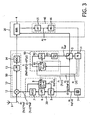
- Fig. 3 shows the block diagram of Fig. 2 in a situation when synchronization has been reached.
- the complete apparatus generates the exact reference frequency of the output signal D that is fed through the switch 3 to the baseband processing unit 20 and possibly to some other parts e.g. a GPS unit that requires this exact reference frequency.
- the conversion signal C is at its exact frequency.
- the reference frequency error ⁇ can be derived, using equation ⁇ 5 ⁇ at the baseband processing unit 20. Therefore, the frequency offset information A is processed, using equation ⁇ 5 ⁇ , due to the fact that the nominal division ratio N.k is known by the set radio channel and the last-programmed frequency correction addend ⁇ -1 is known from the last programming and therefore valid for the conditions at which the actual frequency offset information A was caused.
- ⁇ -1 is either 0 in the initial state or known from a previous setting.
- the frequency correction addend ⁇ +1 for the next step of the PLL-divider 8 and subsequent steps can be programmed or set according to equation ⁇ 6 ⁇ .
- the frequency of the conversion signal C exactly corresponds to the value f ref *(N.k), which corresponds to the exact conversion frequency of the mixer 12.
- the frequency of the conversion signal C comprises the two components (N.k)*f ref and (N.k)* ⁇
- the programming interface 11 controls the selection switch 3 to connect the output signal D of the frequency conversion unit 90 to the baseband processing unit 20.
- the exact reference frequency f ref is used in the receiver arrangement 10 as well as in the baseband processing unit 20, independent from the reference frequency error ⁇ of the uncorrected reference frequency of the reference oscillator signal B.
- the reference frequency error ⁇ changes with time.
- the frequency offset information A of the frequency offset calculator 15 may temporarily deviate from zero.
- a reprogramming of the frequency correction addend ⁇ is performed in the PLL divider 8 and in the coupled multiplier 91 in order to set the frequency offset information A to zero, which corresponds to a reference frequency tracking function for compensating any reference frequency error ⁇ .
- any temporary changes of the synchronization information emitted by the network and received by the mobile terminal which may be caused by Doppler effects and frequency deviations due to frequency offsets at the counterpart station (e.g. base station) cannot be distinguished from changes of the uncorrected reference frequency and are regarded to be represented by the reference frequency error ⁇ .
- a benefit of this arrangement is that, after the frequency correction addend is obtained, the RF section build by the phase locked loop arrangement 30 and the receiver unit 50 need no longer be active for generation of the exact reference frequency of the output signal D. This is valid as long as the frequency error ⁇ does not drastically change. This helps to save current or power and therefore to increase stand-by time.
- a further benefit of this arrangement is that the voltage controlled oscillator 7 can be modulated without coupling or transferring frequency changes to the output signal D.
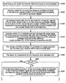
- Fig. 4 shows a schematic flow diagram relating to the change or transfer procedure from the initial state according to Fig. 2 to the synchronized state according to Fig. 3 .
- Fig. 4 depicts a way in which the reference frequency is tracked during the operation of the mobile terminal.
- step S100 the mobile terminal is switched on for reference frequency synchronization.
- step S101 the selection switch 3 connects the reference oscillator signal B of the reference crystal oscillator 2 to the baseband processing unit 20 for activation thereof.
- step S102 the PLL divider 8 is set or programmed to the nominal division ratio N.k, and the correction division ratio (1- ⁇ ) with frequency correction addend ( ⁇ ) equal to 0 is set to the PLL divider 8 and the coupled multiplier 91, and the independent conversion factor ⁇ is set to the coupled multiplier 91 and the coupled divider 92 at the beginning.
- step S103 the selection switch 3 is switched and now connects the output signal D of the frequency conversion unit 90, which frequency at this time corresponds to the uncorrected reference frequency of the reference oscillator signal B of the reference crystal oscillator 2, to the baseband processing unit 20.
- step S104 the voltage-controlled oscillator 7 generates a conversion signal C for the mixer 12, which is still erroneous at this initial point in time.
- step S105 the frequency error information A is generated by the frequency error calculator 15.
- decision step S106 it is checked whether the frequency offset information A is zero or not. If the frequency offset information A is zero, the procedure jumps to step S1 10, where a synchronized operating state is assumed and a waiting time with conditions that depend on decisions made in step S111 is starved. Details and following steps are given within the description of the other branch of the flow diagram.
- step S106 If it is determined in step S106 that the frequency offset information A is not equal zero it is proceeded with step S107.
- the reference frequency error ⁇ of the uncorrected reference frequency of the reference oscillator signal B can be obtained by evaluating the frequency offset information A obtained at the frequency offset calculator 15 by applying equation ⁇ 5 ⁇ .
- the frequency correction addend ⁇ +1 required for next synchronization step is determined by using equation ⁇ 6 ⁇ and is set at the PLL divider 8 and coupled-multiplier 91 in step S108. Then, in step S109, the voltage-controlled oscillator 7 changes the frequency of the conversion signal C to the exact conversion frequency of the mixer 12 and the frequency conversion unit 90 produces the output signal D with the exact reference frequency. Consequently in the following step S110 a synchronized operating state is entered.
- step S111 it is checked whether operation of the RF section (phase locked loop arrangement 30 and receiver unit 50) is necessary for the next waiting time. If so, the waiting time is initiated in step S113 and after the waiting time, the procedure jumps back to step S105.
- step S111 If it is determined in step S111 that operation of the RF section is not necessary, the RF section is switched off in step S112 and the following step is step S113, which initiates a waiting time. After expiry of the waiting time, a decision is made in step S114 whether a new synchronization is wanted. If not, the procedure jumps back to step S113 and a new waiting cycle is initiated. If a new synchronization is wanted, the RF section is switched on in step S115 and the procedure jumps back to step S105.
- the present invention provides the advantage that physical, discrete, analog circuits for frequency tracking at the reference crystal oscillator circuit, such as tuning elements filter and decoupling circuits, can be dispensed with, which leads to savings in costs and space.
- the output signal is decoupled from the voltage-controlled oscillator 7. So the voltage controlled oscillator 7 can be modulated, without having any influence on the spectral quality of the exact reference frequency of the output signal D as output signal.
- the above preferred embodiment as depicted in Figs. 2 , 3 and 4 provides the advantage that the frequency correction addend ⁇ is independent from the set mobile radio channel and independent from the operation as receiver or transmitter.
- an apparatus and method for providing synchronization of an output signal D to a synchronization information or synchronization signal H has been described, wherein the synchronization is accomplished by providing coupling of a correction control information that controls a signal generating means, such as a phase locked loop arrangement 30 or a direct digital synthesis arrangement, to its exact frequency to a frequency conversion unit 90 that converts an uncorrected reference frequency to a correct or exact reference frequency.
- a correction control information that controls a signal generating means, such as a phase locked loop arrangement 30 or a direct digital synthesis arrangement
- a signal generating means such as a phase locked loop arrangement 30 or a direct digital synthesis arrangement
- a conversion signal C is generated on its exact frequency, that is used in the receiver arrangement 10, especially in mixer 12.
- the setting of the phase locked loop arrangement 30 and the frequency conversion unit 90 can be done in a predetermined sequence which enables a user equipment to synchronize its reference frequency to a received frequency correction information emitted by a communication network.
- the present invention is not restricted to the above preferred embodiment and generalized embodiment, but can be applied in any receiver and/or receiver-transmitter arrangement, such as for example superheterodyne receivers, where a clock frequency, reference frequency or other control frequency, which is derived in a terminal device or other device, is synchronized to a comparison frequency derived from or contained in a synchronization information broadcast from a network or made available by other communication media.
- the conversion signal C can also be generated by use of other signal generating means, like for example direct digital synthesis arrangement
- the channel control information is used for generation of the uncorrected conversion signal C.
- the channel control information together with the correction control information is used in order to obtain generation of the exact conversion signal C.
- the synchronization error not necessarily has to be derived from the difference between the frequency f H of the synchronization information H and the frequency f C of the conversion signal C applied to the mixer 12 for conversion to the baseband frequency.
- the synchronization may be derived from a comparison of the frequency f H of the synchronization information H with the frequency f D of the output signal D.
- the synchronization may be derived from a comparison of the frequency f H of the synchronization information H with the frequency f B of the reference oscillator signal B.
- GSM Global System for Mobile communication
- UMTS Universal Mobile Communications System
- CDMA Code Division Multiple Access
- wireless networks such as those specified in IEEE 802.11, IEEE 802.15, IEEE 802.16, Digital Enhanced Cordless Telephone (DECT) systems, Bluetooth systems, and/or any other radio communication standard
- DECT Digital Enhanced Cordless Telephone
Landscapes
- Engineering & Computer Science (AREA)
- Computer Networks & Wireless Communication (AREA)
- Signal Processing (AREA)
- Computer Hardware Design (AREA)
- Microelectronics & Electronic Packaging (AREA)
- Stabilization Of Oscillater, Synchronisation, Frequency Synthesizers (AREA)
- Mobile Radio Communication Systems (AREA)
- Superheterodyne Receivers (AREA)
- Digital Transmission Methods That Use Modulated Carrier Waves (AREA)
- Channel Selection Circuits, Automatic Tuning Circuits (AREA)
Claims (26)
- Synchronisationsvorrichtung zum Synchronisieren eines Ausgangssignals (D) auf Synchronisationsinformationen (H), wobei die Vorrichtung Folgendes umfasst:a) Frequenzumwandlungsmittel (90) zum Umwandeln einer Referenzfrequenz (fref + ε) in eine korrigierte Referenzfrequenz (fref), wobei die Referenzfrequenz zum Verarbeiten der Synchronisationsinformationen (H) verwendet wird;b) Signalerzeugungsmittel (30), dem die Referenzfrequenz zum Erzeugen eines Umwandlungssignals (C) geliefert wird;c) Steuermittel (40) zum Erzeugen von Korrektursteuerinformationen (G) auf der Basis eines festgestellten Synchronisationsfehlers zwischen dem Umwandlungssignal (C) und den Synchronisationsinformationen (H);d) wobei das Steuermittel (40) dafür ausgelegt ist, die Korrektursteuerinformationen an das Frequenzumwandlungsmittel (90) zu liefern zum Korrigieren der Referenzfrequenz auf der Basis der Korrektursteuerinformation;e) wobei das Signalerzeugungsmittel (30) mit Kanalsteuerinformationen (F) programmiert ist, um ein vorbestimmtes Nennunterteilungsverhältnis (N.k) einzustellen und wobei die Korrektursteuerinformationen an das Signalerzeugungsmittel (30) geliefert werden, um ein Frequenzkorrekturunterteilungsverhältnis für das Signalerzeugungsmittel (30) einzustellen (8).
- Synchronisationsvorrichtung nach Anspruch 1, wobei das Signalerzeugungsmittel (30) eine Phasenregelkreisanordnung (5, 6, 7, 8) oder eine Direktdigitalsyntheseanordnung umfasst.
- Synchronisationsvorrichtung nach Anspruch 1 oder 2, weiterhin umfassend einen Referenzoszillator (2) zum Erzeugen der Referenzfrequenz.
- Synchronisationsvorrichtung nach Anspruch 3, wobei der Referenzoszillator (2) ein ungesteuerter Festfrequenzoszillator ist.
- Synchronisationsvorrichtung nach Anspruch 4, wobei der Festfrequenzoszillator (2) ein Quarzoszillator (2) ist.
- Synchronisationsvorrichtung nach Anspruch 4, wobei der Festfrequenzoszillator ein MEMS-Oszillator ist.
- Synchronisationsvorrichtung nach einem der vorhergehenden Ansprüche, wobei die Referenzfrequenz die Basis für ein Kanalumwandlungssignal eines Empfängers ist und wobei das vorbestimmte Nennunterteilungsverhältnis (N.k) von einem Verhältnis zwischen einer Kanalfrequenz des Kanalsignals und einer Nennreferenzfrequenz abgeleitet ist.
- Synchronisationsvorrichtung nach einem der vorhergehenden Ansprüche, wobei das Steuermittel (40) an eine Programmierschnittstelle (11) angeschlossen ist zum Einstellen der Korrektursteuerinformationen und der Kanalsteuerinformationen.
- Synchronisationsvorrichtung nach einem der vorhergehenden Ansprüche, wobei die Korrektursteuerinformationen mindestens einen Frequenzkorrekturaddenden, der von dem Empfangs- oder Übertragungskanal unabhängig ist, und einen unabhängigen Umwandlungsfaktor (p) umfasst.
- Synchronisationsvorrichtung nach Anspruch 9, wobei das Frequenzumwandlungsmittel (90) eine Reihenkombination aus einem Multiplizierermittel (91) und einem Dividierermittel (92) umfasst.
- Synchronisationsvorrichtung nach Anspruch 10, wobei das Multiplizierermittel (91) ausgelegt ist für das Multiplizieren der Referenzfrequenz mit einem Multiplikationsfaktor bestimmt auf der Basis des Frequenzkorrekturaddenden, der von den Korrektursteuerinformationen abgeleitet ist, und dem unabhängigen Umwandlungsfaktor, und wobei das Dividierermittel (92) ausgelegt ist für das Dividieren der multiplizierten Referenzfrequenz mit einem auf der Basis des unabhängigen Umwandlungsfaktors bestimmten Divisionsfaktor.
- Synchronisationsvorrichtung nach einem der vorhergehenden Ansprüche, wobei das Frequenzumwandlungsmittel (90) Filtermittel (93) zum Begrenzen der spektralen Zusammensetzung des Ausgangssignals des Frequenzumwandlungsmittels (90) umfasst.
- Synchronisationsvorrichtung nach Anspruch 11, wobei das Steuermittel (40) dafür ausgelegt ist, den unabhängigen Umwandlungsfaktor so einzustellen, dass ein ganzzahliger Wert des Multiplikationsfaktors erhalten wird.
- Synchronisationsvorrichtung nach Anspruch 11, wobei das Steuermittel (40) dafür ausgelegt ist, den unabhängigen Umwandlungsfaktor so einzustellen, dass ein ganzzahliger Wert des Divisionsfaktors erhalten wird.
- Synchronisationsvorrichtung nach Anspruch 11, wobei der unabhängige Umwandlungsfaktor in der Vorrichtung fest verdrahtet ist.
- Synchronisationsvorrichtung nach einem der vorhergehenden Ansprüche, weiterhin umfassend Schaltmittel (3) zum Liefern entweder der Referenzfrequenz oder eines Ausgangssignals (D) des Frequenzumwandlungsmittels (90) an einen Ausgang der Synchronisationsvorrichtung oder an eine Basisbandverarbeitungseinheit (20).
- Synchronisationsvorrichtung nach einem der vorhergehenden Ansprüche 1 bis 15, wobei das Ausgangssignal (D) an eine Basisbandverarbeitungseinheit (20) geliefert wird.
- Synchronisationsvorrichtung nach Anspruch 16 oder 17, wobei die Basisbandverarbeitungseinheit (20) Berechnungsmittel (15) zum Berechnen des festgestellten Synchronisationsfehlers auf der Basis eines Frequenzoffsets umfasst.
- Synchronisationsverfahren zum Synchronisieren eines Ausgangssignals (D) auf Synchronisationsinformationen (H), wobei das Verfahren die folgenden Schritte umfasst:a) Umwandeln einer Referenzfrequenz (fref + ε) in eine korrigierte Referenzfrequenz (fref), wobei die Referenzfrequenz zum Verarbeiten der Synchronisationsinformationen (H) verwendet wird;b) Liefern der Referenzfrequenz an ein Signalerzeugungsmittel (30), das ein Umwandlungssignal (C) auf der Basis der Referenzfrequenz erzeugt:c) Erzeugen von Korrektursteuerinformationen (G) auf der Basis eines festgestellten Synchronisationsfehlers zwischen dem Umwandlungssignal (C) und den Synchronisationsinformationen (H);d) Verwenden der Korrektursteuerinformationen in dem Umwandlungsschritt a) zum Korrigieren der Referenzfrequenz auf der Basis der Korrektursteuerinformationen;
dadurch gekennzeichnet, dasse) das Umwandlungssignal auf Kanalsteuerinformationen (F) basiert während einer ersten Zeitperiode und das Umwandlungssignal stattdessen auf den Kanalsteuerinformationen und den Korrektursteuerinformationen während einer zweiten nachfolgenden Zeitperiode basiert; und wobei die Kanalsteuerinformationen in dem Schritt b) verwendet werden, um in dem Signalerzeugungsmittel (30) ein vorbestimmtes Nennunterteilungsverhältnis (N.k) einzustellen. - Synchronisationsverfahren nach Anspruch 19, weiterhin umfassend die Schritte des Lieferns der Referenzfrequenz an eine Basisbandverarbeitungseinheit (20) während einer Anfangsbetriebsphase der Basisbandverarbeitungseinheit (20) und Liefern des Ausgangssignals (D) an die Basisbandverarbeitungseinheit (20) nach der Korrektur der Referenzfrequenz.
- Empfängereinrichtung umfassend eine Synchronisationsvorrichtung nach einem der Ansprüche 1 bis 18.
- Sendeempfängereinrichtung umfassend eine Synchronisationsvorrichtung nach einem der Ansprüche 1 bis 18.
- Funkelektronikeinrichtung umfassend eine Synchronisationsvorrichtung nach einem der Ansprüche 1 bis 18.
- Empfängereinrichtung, bei der ein Synchronisationsverfahren nach Anspruch 19 oder 20 verwendet wird.
- Sendeempfängereinrichtung, bei der ein Synchronisationsverfahren nach Anspruch 19 oder 20 verwendet wird.
- Funkelektronikeinrichtung, bei der ein Synchronisationsverfahren nach Anspruch 19 oder 20 verwendet wird.
Priority Applications (1)
| Application Number | Priority Date | Filing Date | Title |
|---|---|---|---|
| EP06765866A EP1900138B1 (de) | 2005-06-29 | 2006-06-26 | Synchronisationsschema mit adaptiver referenzfrequenzkorrektur |
Applications Claiming Priority (3)
| Application Number | Priority Date | Filing Date | Title |
|---|---|---|---|
| EP05105781 | 2005-06-29 | ||
| PCT/IB2006/052085 WO2007000712A1 (en) | 2005-06-29 | 2006-06-26 | Synchronization scheme with adaptive reference frequency correction |
| EP06765866A EP1900138B1 (de) | 2005-06-29 | 2006-06-26 | Synchronisationsschema mit adaptiver referenzfrequenzkorrektur |
Publications (2)
| Publication Number | Publication Date |
|---|---|
| EP1900138A1 EP1900138A1 (de) | 2008-03-19 |
| EP1900138B1 true EP1900138B1 (de) | 2009-11-18 |
Family
ID=37075160
Family Applications (1)
| Application Number | Title | Priority Date | Filing Date |
|---|---|---|---|
| EP06765866A Active EP1900138B1 (de) | 2005-06-29 | 2006-06-26 | Synchronisationsschema mit adaptiver referenzfrequenzkorrektur |
Country Status (7)
| Country | Link |
|---|---|
| US (2) | US8004322B2 (de) |
| EP (1) | EP1900138B1 (de) |
| JP (1) | JP4826968B2 (de) |
| CN (1) | CN101213783B (de) |
| AT (1) | ATE449483T1 (de) |
| DE (1) | DE602006010553D1 (de) |
| WO (1) | WO2007000712A1 (de) |
Families Citing this family (16)
| Publication number | Priority date | Publication date | Assignee | Title |
|---|---|---|---|---|
| DE602006010553D1 (de) * | 2005-06-29 | 2009-12-31 | Nxp Bv | Synchronisationsschema mit adaptiver referenzfrequenzkorrektur |
| US8406702B2 (en) | 2008-03-26 | 2013-03-26 | Freescale Semiconductor, Inc. | Clock signal generating arrangement for a communication device |
| JP4894822B2 (ja) * | 2008-07-04 | 2012-03-14 | 株式会社豊田自動織機 | 周波数補正システム及び受信機 |
| US7994829B2 (en) * | 2009-10-16 | 2011-08-09 | Realtek Semiconductor Corp. | Fast lock-in all-digital phase-locked loop with extended tracking range |
| US8217689B2 (en) * | 2010-01-19 | 2012-07-10 | Integrated Device Technology, Inc. | Method and circuit for DisplayPort video clock recovery |
| US8330644B2 (en) * | 2010-07-14 | 2012-12-11 | The United States Of America As Represented By The Administrator Of The National Aeronautics And Space Administration | Expandable and reconfigurable instrument node arrays |
| US8279014B2 (en) * | 2011-01-07 | 2012-10-02 | Uniband Electronic Corp. | Frequency synthesizer with built-in carrier and crystal oscillation frequency offset cancellation |
| AU2012295802B2 (en) * | 2011-08-12 | 2017-03-30 | Nissan Chemical Industries, Ltd. | Tricyclic heterocyclic compounds and JAK inhibitors |
| US8791762B2 (en) | 2011-10-13 | 2014-07-29 | Sand 9, Inc. | Method and apparatus for managing arbitrary frequencies |
| CA2955510C (en) * | 2014-07-25 | 2018-09-04 | Allen-Vanguard Corporation | System and method for ultra wideband radio frequency scanning and signal generation |
| CN105375921A (zh) * | 2014-08-27 | 2016-03-02 | 硅谷实验室公司 | 使用基于mems的振荡器的准确频率控制 |
| US10826565B2 (en) | 2014-09-05 | 2020-11-03 | Momentum Dynamics Corporation | Near field, full duplex data link for resonant induction wireless charging |
| US11121740B2 (en) | 2014-09-05 | 2021-09-14 | Momentum Dynamics Corporation | Near field, full duplex data link for resonant induction wireless charging |
| CN107112123B (zh) * | 2014-09-05 | 2018-08-07 | 动量动力学公司 | 用于静态和动态谐振感应无线充电的近场全双工数据链路 |
| CN104601317B (zh) * | 2014-12-31 | 2017-12-26 | 南京大全自动化科技有限公司 | 一种fpga的同步时钟装置及其控制方法 |
| US9954542B1 (en) | 2017-02-01 | 2018-04-24 | Apple Inc. | Digital linearization technique for charge pump based fractional phased-locked loop |
Family Cites Families (44)
| Publication number | Priority date | Publication date | Assignee | Title |
|---|---|---|---|---|
| DE2054734C1 (de) * | 1970-11-06 | 1980-10-23 | Siemens Ag, 1000 Berlin Und 8000 Muenchen | Verfahren zur Synchronisation eines Übertragungssystems |
| FR2561468B1 (fr) | 1984-03-13 | 1989-10-20 | Thomson Csf | Filtre actif hyperfrequence |
| JPS6335017A (ja) | 1986-07-30 | 1988-02-15 | Japan Radio Co Ltd | 無線周波数安定化装置 |
| JPS6410748A (en) * | 1987-07-02 | 1989-01-13 | Fujitsu Ltd | Frequency error forcive correction circuit |
| JPH06197140A (ja) * | 1992-10-28 | 1994-07-15 | Hitachi Ltd | ディジタル復調回路 |
| SG72618A1 (en) * | 1993-04-20 | 2000-05-23 | Rca Thomson Licensing | A phase lock loop with error measurement and correction in alternate periods |
| US5497126A (en) * | 1993-11-09 | 1996-03-05 | Motorola, Inc. | Phase synchronization circuit and method therefor for a phase locked loop |
| US5604468A (en) * | 1996-04-22 | 1997-02-18 | Motorola, Inc. | Frequency synthesizer with temperature compensation and frequency multiplication and method of providing the same |
| JP3875347B2 (ja) | 1997-04-08 | 2007-01-31 | 富士通株式会社 | 無線受信機および無線送受信機 |
| US6178216B1 (en) * | 1997-05-21 | 2001-01-23 | Samsung Electronics Co., Ltd. | Digital phase locked loop circuit and method therefor |
| US5856766A (en) * | 1997-06-30 | 1999-01-05 | Motorola Inc. | Communication device with a frequency compensating synthesizer and method of providing same |
| US7221921B2 (en) * | 1998-05-29 | 2007-05-22 | Silicon Laboratories | Partitioning of radio-frequency apparatus |
| JP3439670B2 (ja) * | 1998-10-15 | 2003-08-25 | 富士通株式会社 | 階層型dll回路を利用したタイミングクロック発生回路 |
| US6181195B1 (en) * | 1998-12-23 | 2001-01-30 | Xerox Corporation | Impedance transport circuit |
| US6463266B1 (en) * | 1999-08-10 | 2002-10-08 | Broadcom Corporation | Radio frequency control for communications systems |
| US6259328B1 (en) * | 1999-12-17 | 2001-07-10 | Network Equipment Technologies, Inc. | Method and system for managing reference signals for network clock synchronization |
| DE60035187T2 (de) * | 2000-06-28 | 2008-02-14 | Stmicroelectronics N.V. | Verfahren zur Reduzierung des Elektrizitätsverbrauchs eines zellularen Mobiltelefons |
| JP2003069426A (ja) * | 2001-08-23 | 2003-03-07 | Matsushita Electric Ind Co Ltd | 周波数シンセサイザー |
| JP4608153B2 (ja) * | 2001-09-10 | 2011-01-05 | ルネサスエレクトロニクス株式会社 | チャージポンプ電流補正回路 |
| US6856791B2 (en) | 2002-03-14 | 2005-02-15 | Ericsson Inc. | Direct automatic frequency control method and apparatus |
| US6989698B2 (en) * | 2002-08-26 | 2006-01-24 | Integrant Technologies Inc. | Charge pump circuit for compensating mismatch of output currents |
| CA2442876C (en) * | 2002-09-30 | 2007-01-09 | Vcom Inc. | Timesliced discrete-time phase locked loop |
| US7768360B2 (en) * | 2002-10-15 | 2010-08-03 | Marvell World Trade Ltd. | Crystal oscillator emulator |
| US7760039B2 (en) * | 2002-10-15 | 2010-07-20 | Marvell World Trade Ltd. | Crystal oscillator emulator |
| US7253495B2 (en) * | 2002-10-15 | 2007-08-07 | Marvell World Trade Ltd. | Integrated circuit package with air gap |
| US6744292B2 (en) * | 2002-10-25 | 2004-06-01 | Exar Corporation | Loop filter capacitor multiplication in a charge pump circuit |
| US7064617B2 (en) * | 2003-05-02 | 2006-06-20 | Silicon Laboratories Inc. | Method and apparatus for temperature compensation |
| JP2005079981A (ja) | 2003-09-01 | 2005-03-24 | Sony Corp | 受信機 |
| US7176738B1 (en) * | 2003-11-20 | 2007-02-13 | Integrated Device Technology, Inc. | Method and apparatus for clock generation |
| KR100968296B1 (ko) * | 2003-12-11 | 2010-07-07 | 모사이드 테크놀로지스, 인코포레이티드 | Pll/dll의 고출력 임피던스 충전 펌프 |
| US7161401B2 (en) * | 2004-02-27 | 2007-01-09 | Broadcom Corporation | Wide output-range charge pump with active biasing current |
| US7130225B1 (en) * | 2004-03-03 | 2006-10-31 | Atheros Communications, Inc. | Charge pump with large bypass capacitors |
| US7102400B1 (en) * | 2004-08-30 | 2006-09-05 | Sitel Semiconductor B.V. | Phase locked loop charge pump and method of operation |
| US7141936B2 (en) * | 2004-11-10 | 2006-11-28 | Xerox Corporation | Driving circuit for light emitting diode |
| DE602006010553D1 (de) * | 2005-06-29 | 2009-12-31 | Nxp Bv | Synchronisationsschema mit adaptiver referenzfrequenzkorrektur |
| US7483678B2 (en) * | 2005-09-27 | 2009-01-27 | Skyworks Solutions, Inc. | Single chip GSM/EDGE transceiver architecture with closed loop power control |
| US8014476B2 (en) * | 2005-11-07 | 2011-09-06 | Qualcomm, Incorporated | Wireless device with a non-compensated crystal oscillator |
| US7626462B1 (en) * | 2006-05-02 | 2009-12-01 | Rf Micro Devices, Inc. | Fractional-N based digital AFC system with a translational PLL transmitter |
| US7671648B2 (en) * | 2006-10-27 | 2010-03-02 | Micron Technology, Inc. | System and method for an accuracy-enhanced DLL during a measure initialization mode |
| US7977984B1 (en) * | 2007-10-13 | 2011-07-12 | Altera Corporation | High-speed charge pump circuits |
| US8018269B2 (en) * | 2007-11-13 | 2011-09-13 | Qualcomm Incorporated | Fast-switching low-noise charge pump |
| KR100956770B1 (ko) * | 2007-12-10 | 2010-05-12 | 주식회사 하이닉스반도체 | Dll 회로 및 그 제어 방법 |
| US7847602B2 (en) * | 2008-12-05 | 2010-12-07 | Taitien Electronics Co., Ltd. | Digitally controlled frequency generator |
| US8198927B2 (en) * | 2010-02-01 | 2012-06-12 | Analog Devices, Inc. | High speed charge pump |
-
2006
- 2006-06-26 DE DE602006010553T patent/DE602006010553D1/de active Active
- 2006-06-26 US US11/993,625 patent/US8004322B2/en active Active
- 2006-06-26 JP JP2008519054A patent/JP4826968B2/ja active Active
- 2006-06-26 AT AT06765866T patent/ATE449483T1/de not_active IP Right Cessation
- 2006-06-26 CN CN2006800239923A patent/CN101213783B/zh active Active
- 2006-06-26 WO PCT/IB2006/052085 patent/WO2007000712A1/en not_active Ceased
- 2006-06-26 EP EP06765866A patent/EP1900138B1/de active Active
-
2011
- 2011-06-17 US US13/163,486 patent/US8400195B2/en active Active
Also Published As
| Publication number | Publication date |
|---|---|
| WO2007000712A1 (en) | 2007-01-04 |
| JP4826968B2 (ja) | 2011-11-30 |
| US20110248754A1 (en) | 2011-10-13 |
| US20100156481A1 (en) | 2010-06-24 |
| EP1900138A1 (de) | 2008-03-19 |
| CN101213783B (zh) | 2011-08-31 |
| US8400195B2 (en) | 2013-03-19 |
| US8004322B2 (en) | 2011-08-23 |
| DE602006010553D1 (de) | 2009-12-31 |
| CN101213783A (zh) | 2008-07-02 |
| JP2008547345A (ja) | 2008-12-25 |
| ATE449483T1 (de) | 2009-12-15 |
Similar Documents
| Publication | Publication Date | Title |
|---|---|---|
| US8400195B2 (en) | Synchronization scheme with adaptive reference frequency correction | |
| EP2055003B1 (de) | Referenzsignalerzeugung für mehrere Kommunikationssysteme | |
| EP2713510B1 (de) | Hybrid-AFC mit DCXO und RF PLL | |
| US5493700A (en) | Automatic frequency control apparatus | |
| US10291242B1 (en) | Local oscillator (LO) phase continuity | |
| KR101444966B1 (ko) | 다중 모드 디바이스의 자동 주파수 보정 방법 및 장치 | |
| FI109626B (fi) | Syntetisoijajärjestely ja menetelmä signaalien muodostamiseksi, erityisesti monimoodista radiopuhelinlaitetta varten | |
| US7248658B2 (en) | Method and circuit for deriving a second clock signal from a first clock signal | |
| US7555073B2 (en) | Automatic frequency control loop circuit | |
| US7626462B1 (en) | Fractional-N based digital AFC system with a translational PLL transmitter | |
| US7298809B2 (en) | Self-calibration of a PLL with multiphase clocks | |
| WO2005122407A1 (en) | Synchronization scheme with coupled frequency dividers | |
| JP3698543B2 (ja) | 無線受信機、無線送受信機及び無線受信機用回路 | |
| GB2373113A (en) | Improvements in or relating to fast frequency-hopping synthesisers | |
| JP2752850B2 (ja) | 受信機 | |
| HK1193244A (en) | Hybrid afc using dcxo and rf pll | |
| JP2003046398A (ja) | 受信システム及び送受信システム | |
| JPH05167468A (ja) | 基準信号の周波数校正機能を有する通信装置 | |
| HK1134173A (en) | Reference signal generation for multiple communication systems |
Legal Events
| Date | Code | Title | Description |
|---|---|---|---|
| PUAI | Public reference made under article 153(3) epc to a published international application that has entered the european phase |
Free format text: ORIGINAL CODE: 0009012 |
|
| 17P | Request for examination filed |
Effective date: 20080129 |
|
| AK | Designated contracting states |
Kind code of ref document: A1 Designated state(s): AT BE BG CH CY CZ DE DK EE ES FI FR GB GR HU IE IS IT LI LT LU LV MC NL PL PT RO SE SI SK TR |
|
| DAX | Request for extension of the european patent (deleted) | ||
| 17Q | First examination report despatched |
Effective date: 20080506 |
|
| DAX | Request for extension of the european patent (deleted) | ||
| RAP1 | Party data changed (applicant data changed or rights of an application transferred) |
Owner name: NXP B.V. |
|
| GRAP | Despatch of communication of intention to grant a patent |
Free format text: ORIGINAL CODE: EPIDOSNIGR1 |
|
| GRAS | Grant fee paid |
Free format text: ORIGINAL CODE: EPIDOSNIGR3 |
|
| GRAA | (expected) grant |
Free format text: ORIGINAL CODE: 0009210 |
|
| AK | Designated contracting states |
Kind code of ref document: B1 Designated state(s): AT BE BG CH CY CZ DE DK EE ES FI FR GB GR HU IE IS IT LI LT LU LV MC NL PL PT RO SE SI SK TR |
|
| REG | Reference to a national code |
Ref country code: GB Ref legal event code: FG4D |
|
| REG | Reference to a national code |
Ref country code: CH Ref legal event code: EP |
|
| REG | Reference to a national code |
Ref country code: IE Ref legal event code: FG4D |
|
| REF | Corresponds to: |
Ref document number: 602006010553 Country of ref document: DE Date of ref document: 20091231 Kind code of ref document: P |
|
| REG | Reference to a national code |
Ref country code: NL Ref legal event code: VDEP Effective date: 20091118 |
|
| LTIE | Lt: invalidation of european patent or patent extension |
Effective date: 20091118 |
|
| PG25 | Lapsed in a contracting state [announced via postgrant information from national office to epo] |
Ref country code: ES Free format text: LAPSE BECAUSE OF FAILURE TO SUBMIT A TRANSLATION OF THE DESCRIPTION OR TO PAY THE FEE WITHIN THE PRESCRIBED TIME-LIMIT Effective date: 20100228 Ref country code: SE Free format text: LAPSE BECAUSE OF FAILURE TO SUBMIT A TRANSLATION OF THE DESCRIPTION OR TO PAY THE FEE WITHIN THE PRESCRIBED TIME-LIMIT Effective date: 20091118 Ref country code: IS Free format text: LAPSE BECAUSE OF FAILURE TO SUBMIT A TRANSLATION OF THE DESCRIPTION OR TO PAY THE FEE WITHIN THE PRESCRIBED TIME-LIMIT Effective date: 20100318 Ref country code: PT Free format text: LAPSE BECAUSE OF FAILURE TO SUBMIT A TRANSLATION OF THE DESCRIPTION OR TO PAY THE FEE WITHIN THE PRESCRIBED TIME-LIMIT Effective date: 20100318 Ref country code: LT Free format text: LAPSE BECAUSE OF FAILURE TO SUBMIT A TRANSLATION OF THE DESCRIPTION OR TO PAY THE FEE WITHIN THE PRESCRIBED TIME-LIMIT Effective date: 20091118 Ref country code: FI Free format text: LAPSE BECAUSE OF FAILURE TO SUBMIT A TRANSLATION OF THE DESCRIPTION OR TO PAY THE FEE WITHIN THE PRESCRIBED TIME-LIMIT Effective date: 20091118 |
|
| PG25 | Lapsed in a contracting state [announced via postgrant information from national office to epo] |
Ref country code: PL Free format text: LAPSE BECAUSE OF FAILURE TO SUBMIT A TRANSLATION OF THE DESCRIPTION OR TO PAY THE FEE WITHIN THE PRESCRIBED TIME-LIMIT Effective date: 20091118 Ref country code: SI Free format text: LAPSE BECAUSE OF FAILURE TO SUBMIT A TRANSLATION OF THE DESCRIPTION OR TO PAY THE FEE WITHIN THE PRESCRIBED TIME-LIMIT Effective date: 20091118 Ref country code: LV Free format text: LAPSE BECAUSE OF FAILURE TO SUBMIT A TRANSLATION OF THE DESCRIPTION OR TO PAY THE FEE WITHIN THE PRESCRIBED TIME-LIMIT Effective date: 20091118 Ref country code: CY Free format text: LAPSE BECAUSE OF FAILURE TO SUBMIT A TRANSLATION OF THE DESCRIPTION OR TO PAY THE FEE WITHIN THE PRESCRIBED TIME-LIMIT Effective date: 20091118 |
|
| PG25 | Lapsed in a contracting state [announced via postgrant information from national office to epo] |
Ref country code: AT Free format text: LAPSE BECAUSE OF FAILURE TO SUBMIT A TRANSLATION OF THE DESCRIPTION OR TO PAY THE FEE WITHIN THE PRESCRIBED TIME-LIMIT Effective date: 20091118 Ref country code: BE Free format text: LAPSE BECAUSE OF FAILURE TO SUBMIT A TRANSLATION OF THE DESCRIPTION OR TO PAY THE FEE WITHIN THE PRESCRIBED TIME-LIMIT Effective date: 20091118 |
|
| PG25 | Lapsed in a contracting state [announced via postgrant information from national office to epo] |
Ref country code: BG Free format text: LAPSE BECAUSE OF FAILURE TO SUBMIT A TRANSLATION OF THE DESCRIPTION OR TO PAY THE FEE WITHIN THE PRESCRIBED TIME-LIMIT Effective date: 20100218 Ref country code: EE Free format text: LAPSE BECAUSE OF FAILURE TO SUBMIT A TRANSLATION OF THE DESCRIPTION OR TO PAY THE FEE WITHIN THE PRESCRIBED TIME-LIMIT Effective date: 20091118 Ref country code: NL Free format text: LAPSE BECAUSE OF FAILURE TO SUBMIT A TRANSLATION OF THE DESCRIPTION OR TO PAY THE FEE WITHIN THE PRESCRIBED TIME-LIMIT Effective date: 20091118 Ref country code: DK Free format text: LAPSE BECAUSE OF FAILURE TO SUBMIT A TRANSLATION OF THE DESCRIPTION OR TO PAY THE FEE WITHIN THE PRESCRIBED TIME-LIMIT Effective date: 20091118 Ref country code: RO Free format text: LAPSE BECAUSE OF FAILURE TO SUBMIT A TRANSLATION OF THE DESCRIPTION OR TO PAY THE FEE WITHIN THE PRESCRIBED TIME-LIMIT Effective date: 20091118 |
|
| PG25 | Lapsed in a contracting state [announced via postgrant information from national office to epo] |
Ref country code: CZ Free format text: LAPSE BECAUSE OF FAILURE TO SUBMIT A TRANSLATION OF THE DESCRIPTION OR TO PAY THE FEE WITHIN THE PRESCRIBED TIME-LIMIT Effective date: 20091118 Ref country code: SK Free format text: LAPSE BECAUSE OF FAILURE TO SUBMIT A TRANSLATION OF THE DESCRIPTION OR TO PAY THE FEE WITHIN THE PRESCRIBED TIME-LIMIT Effective date: 20091118 |
|
| PLBE | No opposition filed within time limit |
Free format text: ORIGINAL CODE: 0009261 |
|
| STAA | Information on the status of an ep patent application or granted ep patent |
Free format text: STATUS: NO OPPOSITION FILED WITHIN TIME LIMIT |
|
| 26N | No opposition filed |
Effective date: 20100819 |
|
| PG25 | Lapsed in a contracting state [announced via postgrant information from national office to epo] |
Ref country code: GR Free format text: LAPSE BECAUSE OF FAILURE TO SUBMIT A TRANSLATION OF THE DESCRIPTION OR TO PAY THE FEE WITHIN THE PRESCRIBED TIME-LIMIT Effective date: 20100219 |
|
| PG25 | Lapsed in a contracting state [announced via postgrant information from national office to epo] |
Ref country code: MC Free format text: LAPSE BECAUSE OF NON-PAYMENT OF DUE FEES Effective date: 20100630 |
|
| REG | Reference to a national code |
Ref country code: CH Ref legal event code: PL |
|
| PG25 | Lapsed in a contracting state [announced via postgrant information from national office to epo] |
Ref country code: IT Free format text: LAPSE BECAUSE OF FAILURE TO SUBMIT A TRANSLATION OF THE DESCRIPTION OR TO PAY THE FEE WITHIN THE PRESCRIBED TIME-LIMIT Effective date: 20091118 |
|
| PG25 | Lapsed in a contracting state [announced via postgrant information from national office to epo] |
Ref country code: IE Free format text: LAPSE BECAUSE OF NON-PAYMENT OF DUE FEES Effective date: 20100626 Ref country code: LI Free format text: LAPSE BECAUSE OF NON-PAYMENT OF DUE FEES Effective date: 20100630 Ref country code: CH Free format text: LAPSE BECAUSE OF NON-PAYMENT OF DUE FEES Effective date: 20100630 |
|
| PG25 | Lapsed in a contracting state [announced via postgrant information from national office to epo] |
Ref country code: HU Free format text: LAPSE BECAUSE OF FAILURE TO SUBMIT A TRANSLATION OF THE DESCRIPTION OR TO PAY THE FEE WITHIN THE PRESCRIBED TIME-LIMIT Effective date: 20100519 Ref country code: LU Free format text: LAPSE BECAUSE OF NON-PAYMENT OF DUE FEES Effective date: 20100626 |
|
| PG25 | Lapsed in a contracting state [announced via postgrant information from national office to epo] |
Ref country code: TR Free format text: LAPSE BECAUSE OF FAILURE TO SUBMIT A TRANSLATION OF THE DESCRIPTION OR TO PAY THE FEE WITHIN THE PRESCRIBED TIME-LIMIT Effective date: 20091118 |
|
| REG | Reference to a national code |
Ref country code: GB Ref legal event code: 732E Free format text: REGISTERED BETWEEN 20141120 AND 20141126 |
|
| REG | Reference to a national code |
Ref country code: FR Ref legal event code: TP Owner name: ST-ERICSSON SA, CH Effective date: 20141117 |
|
| REG | Reference to a national code |
Ref country code: FR Ref legal event code: CD Owner name: ST-ERICSSON SA, CH Effective date: 20141211 |
|
| REG | Reference to a national code |
Ref country code: DE Ref legal event code: R082 Ref document number: 602006010553 Country of ref document: DE Representative=s name: CASALONGA & PARTNERS, DE |
|
| REG | Reference to a national code |
Ref country code: FR Ref legal event code: CD Owner name: ST-ERICSSON SA, CH Effective date: 20150203 |
|
| REG | Reference to a national code |
Ref country code: DE Ref legal event code: R082 Ref document number: 602006010553 Country of ref document: DE Representative=s name: CASALONGA & PARTNERS, DE Effective date: 20150129 Ref country code: DE Ref legal event code: R081 Ref document number: 602006010553 Country of ref document: DE Owner name: ST-ERICSSON SA, PLAN-LES-OUATES, CH Free format text: FORMER OWNER: NXP B.V., EINDHOVEN, NL Effective date: 20150129 Ref country code: DE Ref legal event code: R081 Ref document number: 602006010553 Country of ref document: DE Owner name: SNAPTRACK INC., SAN DIEGO, US Free format text: FORMER OWNER: NXP B.V., EINDHOVEN, NL Effective date: 20150129 |
|
| REG | Reference to a national code |
Ref country code: DE Ref legal event code: R082 Ref document number: 602006010553 Country of ref document: DE Representative=s name: CASALONGA & PARTNERS, DE |
|
| REG | Reference to a national code |
Ref country code: FR Ref legal event code: PLFP Year of fee payment: 10 |
|
| REG | Reference to a national code |
Ref country code: DE Ref legal event code: R081 Ref document number: 602006010553 Country of ref document: DE Owner name: SNAPTRACK INC., SAN DIEGO, US Free format text: FORMER OWNER: ST-ERICSSON SA, PLAN-LES-OUATES, GENEVA, CH Effective date: 20150511 Ref country code: DE Ref legal event code: R082 Ref document number: 602006010553 Country of ref document: DE Representative=s name: CASALONGA & PARTNERS, DE Effective date: 20150511 |
|
| REG | Reference to a national code |
Ref country code: GB Ref legal event code: 732E Free format text: REGISTERED BETWEEN 20150611 AND 20150617 |
|
| REG | Reference to a national code |
Ref country code: FR Ref legal event code: TP Owner name: SNAPTRACK, INC., US Effective date: 20151112 |
|
| REG | Reference to a national code |
Ref country code: FR Ref legal event code: PLFP Year of fee payment: 11 |
|
| REG | Reference to a national code |
Ref country code: FR Ref legal event code: PLFP Year of fee payment: 12 |
|
| REG | Reference to a national code |
Ref country code: FR Ref legal event code: PLFP Year of fee payment: 13 |
|
| PGFP | Annual fee paid to national office [announced via postgrant information from national office to epo] |
Ref country code: DE Payment date: 20250509 Year of fee payment: 20 |
|
| PGFP | Annual fee paid to national office [announced via postgrant information from national office to epo] |
Ref country code: GB Payment date: 20250508 Year of fee payment: 20 |
|
| PGFP | Annual fee paid to national office [announced via postgrant information from national office to epo] |
Ref country code: FR Payment date: 20250512 Year of fee payment: 20 |