EP1872402B1 - Structure de transistors a effet de champ en parallele a contact etabli avec le corps - Google Patents
Structure de transistors a effet de champ en parallele a contact etabli avec le corps Download PDFInfo
- Publication number
- EP1872402B1 EP1872402B1 EP06758334A EP06758334A EP1872402B1 EP 1872402 B1 EP1872402 B1 EP 1872402B1 EP 06758334 A EP06758334 A EP 06758334A EP 06758334 A EP06758334 A EP 06758334A EP 1872402 B1 EP1872402 B1 EP 1872402B1
- Authority
- EP
- European Patent Office
- Prior art keywords
- region
- fet
- gate conductor
- conductor portion
- source
- Prior art date
- Legal status (The legal status is an assumption and is not a legal conclusion. Google has not performed a legal analysis and makes no representation as to the accuracy of the status listed.)
- Not-in-force
Links
- 230000005669 field effect Effects 0.000 title claims abstract description 11
- 239000004020 conductor Substances 0.000 claims abstract description 83
- 239000004065 semiconductor Substances 0.000 claims description 47
- 239000013078 crystal Substances 0.000 claims description 39
- 239000000758 substrate Substances 0.000 claims description 24
- 238000009792 diffusion process Methods 0.000 claims description 16
- 239000012212 insulator Substances 0.000 claims description 9
- 230000003071 parasitic effect Effects 0.000 abstract description 7
- 238000002955 isolation Methods 0.000 description 8
- 229910021332 silicide Inorganic materials 0.000 description 6
- FVBUAEGBCNSCDD-UHFFFAOYSA-N silicide(4-) Chemical compound [Si-4] FVBUAEGBCNSCDD-UHFFFAOYSA-N 0.000 description 6
- 238000000034 method Methods 0.000 description 5
- 230000007704 transition Effects 0.000 description 5
- XUIMIQQOPSSXEZ-UHFFFAOYSA-N Silicon Chemical compound [Si] XUIMIQQOPSSXEZ-UHFFFAOYSA-N 0.000 description 3
- 238000004519 manufacturing process Methods 0.000 description 3
- 229910052710 silicon Inorganic materials 0.000 description 3
- 239000010703 silicon Substances 0.000 description 3
- 125000006850 spacer group Chemical group 0.000 description 3
- 229910000577 Silicon-germanium Inorganic materials 0.000 description 2
- LEVVHYCKPQWKOP-UHFFFAOYSA-N [Si].[Ge] Chemical compound [Si].[Ge] LEVVHYCKPQWKOP-UHFFFAOYSA-N 0.000 description 2
- 238000001514 detection method Methods 0.000 description 2
- 230000000694 effects Effects 0.000 description 2
- 238000005516 engineering process Methods 0.000 description 2
- 239000007943 implant Substances 0.000 description 2
- 229910021421 monocrystalline silicon Inorganic materials 0.000 description 2
- 230000000630 rising effect Effects 0.000 description 2
- 229910000676 Si alloy Inorganic materials 0.000 description 1
- 238000009825 accumulation Methods 0.000 description 1
- 238000000137 annealing Methods 0.000 description 1
- 239000002800 charge carrier Substances 0.000 description 1
- 238000000151 deposition Methods 0.000 description 1
- -1 e.g. Inorganic materials 0.000 description 1
- 239000011810 insulating material Substances 0.000 description 1
- 239000002184 metal Substances 0.000 description 1
- 230000005855 radiation Effects 0.000 description 1
- 239000002210 silicon-based material Substances 0.000 description 1
Images


Classifications
-
- H—ELECTRICITY
- H01—ELECTRIC ELEMENTS
- H01L—SEMICONDUCTOR DEVICES NOT COVERED BY CLASS H10
- H01L27/00—Devices consisting of a plurality of semiconductor or other solid-state components formed in or on a common substrate
- H01L27/02—Devices consisting of a plurality of semiconductor or other solid-state components formed in or on a common substrate including semiconductor components specially adapted for rectifying, oscillating, amplifying or switching and having potential barriers; including integrated passive circuit elements having potential barriers
- H01L27/12—Devices consisting of a plurality of semiconductor or other solid-state components formed in or on a common substrate including semiconductor components specially adapted for rectifying, oscillating, amplifying or switching and having potential barriers; including integrated passive circuit elements having potential barriers the substrate being other than a semiconductor body, e.g. an insulating body
- H01L27/1203—Devices consisting of a plurality of semiconductor or other solid-state components formed in or on a common substrate including semiconductor components specially adapted for rectifying, oscillating, amplifying or switching and having potential barriers; including integrated passive circuit elements having potential barriers the substrate being other than a semiconductor body, e.g. an insulating body the substrate comprising an insulating body on a semiconductor body, e.g. SOI
-
- H—ELECTRICITY
- H01—ELECTRIC ELEMENTS
- H01L—SEMICONDUCTOR DEVICES NOT COVERED BY CLASS H10
- H01L27/00—Devices consisting of a plurality of semiconductor or other solid-state components formed in or on a common substrate
- H01L27/02—Devices consisting of a plurality of semiconductor or other solid-state components formed in or on a common substrate including semiconductor components specially adapted for rectifying, oscillating, amplifying or switching and having potential barriers; including integrated passive circuit elements having potential barriers
- H01L27/04—Devices consisting of a plurality of semiconductor or other solid-state components formed in or on a common substrate including semiconductor components specially adapted for rectifying, oscillating, amplifying or switching and having potential barriers; including integrated passive circuit elements having potential barriers the substrate being a semiconductor body
- H01L27/08—Devices consisting of a plurality of semiconductor or other solid-state components formed in or on a common substrate including semiconductor components specially adapted for rectifying, oscillating, amplifying or switching and having potential barriers; including integrated passive circuit elements having potential barriers the substrate being a semiconductor body including only semiconductor components of a single kind
- H01L27/085—Devices consisting of a plurality of semiconductor or other solid-state components formed in or on a common substrate including semiconductor components specially adapted for rectifying, oscillating, amplifying or switching and having potential barriers; including integrated passive circuit elements having potential barriers the substrate being a semiconductor body including only semiconductor components of a single kind including field-effect components only
- H01L27/088—Devices consisting of a plurality of semiconductor or other solid-state components formed in or on a common substrate including semiconductor components specially adapted for rectifying, oscillating, amplifying or switching and having potential barriers; including integrated passive circuit elements having potential barriers the substrate being a semiconductor body including only semiconductor components of a single kind including field-effect components only the components being field-effect transistors with insulated gate
-
- H—ELECTRICITY
- H01—ELECTRIC ELEMENTS
- H01L—SEMICONDUCTOR DEVICES NOT COVERED BY CLASS H10
- H01L29/00—Semiconductor devices specially adapted for rectifying, amplifying, oscillating or switching and having potential barriers; Capacitors or resistors having potential barriers, e.g. a PN-junction depletion layer or carrier concentration layer; Details of semiconductor bodies or of electrodes thereof ; Multistep manufacturing processes therefor
- H01L29/66—Types of semiconductor device ; Multistep manufacturing processes therefor
- H01L29/68—Types of semiconductor device ; Multistep manufacturing processes therefor controllable by only the electric current supplied, or only the electric potential applied, to an electrode which does not carry the current to be rectified, amplified or switched
- H01L29/76—Unipolar devices, e.g. field effect transistors
- H01L29/772—Field effect transistors
- H01L29/78—Field effect transistors with field effect produced by an insulated gate
- H01L29/786—Thin film transistors, i.e. transistors with a channel being at least partly a thin film
- H01L29/78606—Thin film transistors, i.e. transistors with a channel being at least partly a thin film with supplementary region or layer in the thin film or in the insulated bulk substrate supporting it for controlling or increasing the safety of the device
- H01L29/78612—Thin film transistors, i.e. transistors with a channel being at least partly a thin film with supplementary region or layer in the thin film or in the insulated bulk substrate supporting it for controlling or increasing the safety of the device for preventing the kink- or the snapback effect, e.g. discharging the minority carriers of the channel region for preventing bipolar effect
- H01L29/78615—Thin film transistors, i.e. transistors with a channel being at least partly a thin film with supplementary region or layer in the thin film or in the insulated bulk substrate supporting it for controlling or increasing the safety of the device for preventing the kink- or the snapback effect, e.g. discharging the minority carriers of the channel region for preventing bipolar effect with a body contact
-
- H—ELECTRICITY
- H01—ELECTRIC ELEMENTS
- H01L—SEMICONDUCTOR DEVICES NOT COVERED BY CLASS H10
- H01L29/00—Semiconductor devices specially adapted for rectifying, amplifying, oscillating or switching and having potential barriers; Capacitors or resistors having potential barriers, e.g. a PN-junction depletion layer or carrier concentration layer; Details of semiconductor bodies or of electrodes thereof ; Multistep manufacturing processes therefor
- H01L29/66—Types of semiconductor device ; Multistep manufacturing processes therefor
- H01L29/68—Types of semiconductor device ; Multistep manufacturing processes therefor controllable by only the electric current supplied, or only the electric potential applied, to an electrode which does not carry the current to be rectified, amplified or switched
- H01L29/76—Unipolar devices, e.g. field effect transistors
- H01L29/772—Field effect transistors
- H01L29/78—Field effect transistors with field effect produced by an insulated gate
- H01L29/7833—Field effect transistors with field effect produced by an insulated gate with lightly doped drain or source extension, e.g. LDD MOSFET's; DDD MOSFET's
Definitions
- the present invention relates to semiconductor device structures, and more particularly to a field effect transistor structure ("FET”) having a body contact.
- FET field effect transistor structure
- Speed is a key aspect of operational performance of integrated circuits.
- enhanced fabrication techniques including silicon-on-insulator (SOI) technology have been introduced.
- SOI technology is becoming increasingly important since it assists in lowering the capacitance of transistors, enabling greater switching speeds.
- FETs typically have a voltage-controlled source-drain conduction path extending between a source region, through a channel region and into a drain region of the FET.
- Another way that a FET can be considered is that each FET has two source/drain regions, one disposed at each end of the channel region, instead of making a distinction between the one source region and one drain region.
- FETs When FETs are formed in bulk substrates, the junctions between the source/drain regions and the well region surrounding the transistor and between the well region and the body of the transistor (the portion of the transistor immediately below the gate including the transistor channel), result in significant capacitance.
- active devices such as field effect transistors ("FETs") are formed in a relatively thin single-crystal semiconductor layer overlying a buried layer of insulating material such as a buried oxide (BOX) layer.
- BOX buried oxide
- Most of the capacitance associated with the junctions between the source/drain regions and the surrounding well region is eliminated in a design including an SOI substrate, because the heavily-doped source/drain region is isolated from the substrate by the presence of the buried oxide.
- the body of the SOI FET is, as a result, electrically isolated.
- the electrically isolated body of a transistor having a conduction channel formed in an SOI substrate is known as a "floating body" because the body floats at a potential which varies according to various conditions in which the transistor is operated, wherein such potential is usually not known in advance.
- the threshold voltage V T of the transistor is subject to variation, also to an extent that is usually not known in advance.
- the threshold voltage V T is the voltage at which an FET transitions from an 'off' state to an 'on' state.
- FETs are fabricated as either n-channel type FETs (NFETs) or p-channel type FETs (PFETs).
- the threshold voltage V T may be lowered, causing the NFET to turn on at too low a voltage, early within a switching cycle. This may cause an early or false detection signal for rising signal transitions. Conversely, for falling signal transitions, detection comes later than expected. In addition, a lower value of the low voltage is required to keep the subthreshold leakage current tolerably low. Alternatively, the threshold voltage V T may increase as a result of charge accumulation, causing the NFET to turn on late for rising signal transitions and early in the case of falling signal transitions. While such variations in the threshold voltage are usually tolerable when the FET is used in a digital switching element such as an inverter or logic gate, FETs used for amplifying signals, especially small swing signals, need to have a stable threshold voltage.
- a body contact for the field effect transistor having a conduction channel disposed in an SOI substrate.
- a body contact is an electrically conductive contact made to the body of the transistor to provide, inter alia , a low-resistance path for the flow of charge carriers to and from the transistor body.
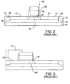
- FIG. 1 is a plan view illustrating a prior art FET 100 having a conduction channel (not shown) formed in a SOI region of a substrate, the FET having a body contact.
- the particular SOI region in which the FET is formed is also referred to herein as an active area 110, as bounded by one or more isolation regions 122.
- the FET 100 includes a conductor pattern 104 having a gate conductor portion 102 which extends in a direction of the length 115 of the active area 110.
- the gate conductor portion 102 divides the width 120 of the active area 110 into three parts: a source region 113 disposed between a left edge 106 of the active area and the gate conductor portion 102, a channel region (not shown) of the FET underlying the gate conductor portion 102, and a drain region 114 disposed between the gate conductor portion 102 and a right edge 108 of the active area 110.
- FIG. 2 is a sectional view of the SOI FET through line 2-2 of FIG. 1 .
- the body 160 of the FET 100 is disposed in an active area 110 of a scmiconductor-on-insulator ("SOI") region such as a silicon-on-insulator layer of an SOI substrate 90.
- SOI scmiconductor-on-insulator
- the active area 110 is bounded by one or more isolation regions 122 disposed at left and right edges 106, 108 of the active area 110, as well as at the top edge 124 and the bottom edge 126 of the active area ( FIG. 1 ).
- the SOI region overlies a buried oxide (“BOX”) layer 103, which insulates the SOI region from a bulk region 107 of the substrate 90.
- BOX buried oxide
- the body 160 of the FET is disposed under the gate conductor portion 102.
- a channel region 120 occupies a portion of the body 160 close to a gate dielectric 115 of the FET.
- the source region 113 and the drain region occupy portions of the active area 110 adjacent to the body 160.
- a conductive body contact via 170 conductively contacts a portion of the active area 110 of the FET adjacent to the body 160 of the FET.
- the FET is an NFET in which the body has p-type doping.
- the NFET is turned on when a sufficient concentration of electrons accumulates to produce an inversion layer in the channel region 120 ( FIG. 1 ) having n-type conductivity.
- the body contact has p+ doping in order to provide a conductive path to the p-type doped body 160 of the NFET. This differs from the n+ type doping used for the source region 113 and drain region 114 of the NFET 100 ( FIGS. 1-2 ).
- body contacts is particularly advantageous in circuitry involving current sources, current mirror circuits or when used in conjunction with sense amplifiers when data signals need to be amplified.
- body contact designs are used in partially depleted SOI FET devices in order to minimize the floating charge body effects.
- transistor designs include body contacts sparingly because a body contact tends to increase the amount of substrate area that the FET occupies, as well as the capacitance between the gate conductor of the FET and the SOI layer under the gate. Each of these also tends to degrade the performance of the FET in a circuit.
- the increase in surface area is best viewed in the top down depiction of FIG. 1 , where the conductor pattern 104 includes the gate conductor portion 102 and a large body contact conductor portion 170 connected thereto.
- the large body contact conductor portion 170 being in capacitive contact with the active area, adds large parasitic capacitance.
- the area underlying of the large conductor portion 170 does not lie in the area between the source region and the drain region of the FET, the area is not used for driving the on current of the FET as it is for the area under the gate conductor portion 102.
- the increase in capacitance impacts the switching speed of the FET.
- the increased area of the large body contact conductor portion further impacts the switching speed of the FET by increasing the length of wiring to the FET. To counter the effects of increased capacitance, the drive current would need to be increased to maintain the original switching speed. Besides being difficult to accomplish, such would cause an undesirable increase in power dissipation.
- FIG. 4 is a plan view illustrating a different prior art body-contacted FET 200 in which a body contact conductor portion 270 of the gate conductor pattern has reduced area compared to the area of the body contact conductor portion 170 of FET 100 ( FIG. 1 ).
- This FET 200 has two gate conductor fingers 202 which extend in a direction of the length 215 of an active area 210, and includes two source regions 213 which are separated from a common drain region 214 by the fingers.
- the two fingers 202 are placed parallel to each other, dividing the width 240 of the active area 210 into three parts, the two source regions 213 provided between the fingers 210 and the outer edges of the active area 210 and the drain 214 provided between the two fingers 202.
- the two-finger design of FET 200 is advantageous because it provides increased current drive over a one-finger design of FET 100 which occupies an active area having the same width as width 120 of FET 100 ( FIG. 1 ).
- the body contact conductor portion 270 does not separate the source regions 213 of the active area 210 from the body contact 272, as it did in the FET 100 ( FIG. 1 ). As a result, the source regions 213 are not electrically isolated from the body contact 272. This limits the applications to which the FET 200 can be put, since the voltages applied to the source regions and the body contact must be kept the same, e.g., at ground.
- FIG. 5 shows another body-contacted FET 300 according to the prior art.
- a body-contact portion 372 of the active area is implanted to p+ doping.
- This FET 300 has a design which has lowered parasitic capacitance in relation to FET 100 shown in FIG. 1 , because the amount of the semiconductor area underlying the body-contact portion 370 of the conductor pattern is less than that shown in FIG. 1 .
- the design shown in FIG. 5 is rarely used, because it requires a large amount of semiconductor area 380 to provide the body contact relative to the amount of semiconductor area 390 used to provide the active FET 300.
- one difficulty with the use of a body contact is large parasitic capacitance.
- the large capacitance arises because of the close proximity between the body contact conductor portion 170 ( FIG. 1 ), 270 ( FIG. 4 ) or 370 ( FIG. 5 ) and the single-crystal SOI region of the substrate across a portion of the gate dielectric layer 115 ( FIG. 3 ).
- US patent application 2005/0023608 A1 discloses a method of forming a partially depleted silicon on insulator (PDSOI) transistor with a pad lock body extension.
- PDSOI partially depleted silicon on insulator
- US patent 5,821,575 disloses a compact self-aligned body contact silicon-on-insulator transistor.
- US patent application 2003/0052373 A1 discloses a field effect transistor formed on an insulating substrate and integrated circuit therof.
- US patent 5,811,855 discloses an H-transistor, fabricated on an SOI substrate.
- US patent 6,399,989 B1 discloses a radiation hardened silicon-on-insulator (SOI) transistor having a body contact.
- European patent application 1,783,836 A2 discloses a semiconductor device that eliminates at least one of the channel/dielectric interfaces along the side walls of a SOI/SOS transistor channel.
- the embodiments of the invention provided herein address the foregoing problems by separating a first or primary field effect transistor ("FET") from a body contact thereto by one or more second FETs that are placed electrically in parallel with the first FET.
- FET primary field effect transistor
- the gate conductor of the first FET and gate conductor of the second FET are integral parts of a unitary conductive pattern.
- the unitary conductive pattern is made desirably small, and can be made as the smallest predetermined linewidth for gate conductors on an integrated circuit which includes the body-contacted FET. In this way, area and parasitic capacitance are kept small.
- the invention provides a semiconductor device structure as claimed in claim 1.
- a semiconductor device structure and fabrication method are provided which address the foregoing problems of body-contacted FETs.
- a first field effect transistor (FET) 620 is disposed in a unitary single-crystal semiconductor region 600 of a substrate.
- a body contact 640 has a junction 642 to a diffusion region 650 of the unitary single-crystal region 600 that is not electrically tied to the source region 624 of the first FET or indeed to the drain region 626 of the first FET.
- the diffusion region 650 functions as at least one of a source region and a drain region of a second FET 632 and that of another second FET 634 having a source-drain conduction path to at least one of the first source region and first drain region of the first FET.
- the source-drain conduction path of the second FET is electrically connected in parallel with the source-drain conduction path of the first FET.
- the unitary single-crystal semiconductor region 600 preferably consists essentially of silicon or consists essentially of an alloy of silicon, e.g., silicon germanium.
- the semiconductor region 600 has a portion consisting essentially of silicon and another portion consisting essentially of silicon germanium for the purpose of applying a stress to the channel region to increase the performance of the transistor.
- the unitary single-crystal region is optionally bounded by one or more regions of shallow trench isolation ("STI") 610 disposed at a bottom edge 616 and at a top edge 618 of the single-crystal region 600 and at a left edge 612 and at a right edge 614 of the unitary single-crystal semiconductor region 600.
- STI shallow trench isolation
- the unitary single-crystal region 600 is preferably provided in a semiconductor-on-insulator ("SOI") layer such as a silicon-on-insulator layer of an SOI substrate in which a buried oxide (“BOX”) layer underlies the SOI layer and a bulk region of the substrate underlies the BOX layer, similar to the BOX layer and bulk region shown and described above with reference to FIG. 2 .
- SOI semiconductor-on-insulator
- BOX buried oxide
- the first FET 620 has a first source-drain conduction path 622 between a first source region 624 and a first drain region 626 in the unitary single-crystal semiconductor region 600.
- a body contact 640 has a junction 642 to a diffusion region 650 of the unitary single-crystal region 600 that is not electrically tied to the source region 624 of the first FET or indeed to the drain region 626 of the first FET. Instead, a portion of the diffusion region 650 functions as a source region 652 of a second FET 632 having a source-drain conduction path 633 to a drain region 626 of the first FET 620 which is in parallel with the source-drain conduction path 622 of the first FET. Similarly, a portion of the diffusion region 650 functions as a drain region 654 of another second FET 634 having a source-drain conduction path 635 to the source region 624 of the first FET 620 in parallel with the first FET.
- the first FET and second FETs have gate conductors, respectively, provided as a first gate conductor portion 660, and second gate conductor portions 662, 664, respectively, which are conductively and physically joined together in one unitary conductive pattern.
- the first gate conductor portion 660 is oriented in a lengthwise direction of the unitary single-crystal region 600, i.e., the direction between the top and bottom edges 618, 616 of the unitary single-crystal region 600.
- the second gate conductor portions 662, 664 are oriented in a widthwise direction of the unitary single-crystal region, i.e., the direction of the width 665 between the left and right edges 612, 614 of the unitary single-crystal region.
- the unitary conductive pattern also includes a tail conductor 670 extending in the lengthwise direction from an edge of the second gate conductor portions 662, 664 towards the top edge 618 of the unitary conductive pattern.
- the second gate conductor portions 662, 664 of the unitary conductive pattern extend entirely across the width 665. This helps to assure that the diffusion region 650, in which portions of the second FETs 632, 634 are disposed, is electrically separate from the first FET 620.
- the first gate conductor portion 660 extends all the way from one edge of the second gate conductor portions 662, 664 to one edge of the unitary single-crystal semiconductor region 600, in this case the bottom edge 616.
- the unitary conductive pattern has a linewidth 670 which is not substantially greater than a predetermined smallest linewidth for gate conductors of the integrated circuit of which the semiconductor device structure forms a part.
- the linewidth 670 of the unitary conductive pattern is equal to the smallest predetermined linewidth for the integrated circuit.
- Small linewidth facilitates high current drive through the first FET 620.
- Small linewidth also reduces the amount of the single-crystal semiconductor region underlying portions of the conductive pattern that is not utilized as a first gate conductor of the first FET, thus keeping parasitic capacitance low.
- the body contact 640 is formed by implanting a somewhat heavily doped region into the unitary single-crystal semiconductor region through a corresponding opening.
- the opening may extend over a portion of the STI region 610, such that some of the implanted species are implanted into the STI region 610 when the body contact region is implanted.
- the implanted portion of the unitary single-crystal semiconductor region 600 becomes a part of the body contact region of the structure.
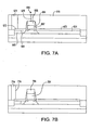
- FIG. 7A is a sectional view through lines 7-7 of the semiconductor device structure shown in FIG. 6 .
- the body contact region 640 of the single-crystal semiconductor region is adjacent to and forms a junction with the diffusion region 654.
- the second diffusion region 654 functions as a drain region for the second FET.
- the second FET 634 has a source-drain conduction path extending between the diffusion region 654 under the second gate conductor portion 664 to the source region 624 of the first FET.
- a silicide layer 672 overlies the SOI layer in which the body contact region 640, the second diffusion region 654 and the first source region 624 are disposed.
- the silicide layer 672 is preferably formed by depositing a silicide-forming metal onto the exposed single-crystal silicon material of the structure and then annealing to form the silicide 672 which is self-aligned to the single-crystal silicon region.
- An interlevel dielectric (“ILD") region 676 covers the semiconductor device structure including all the FETs, the body contact areas, and the diffusion regions. Contacts, such as conductive via 674 and other contacts (not shown) may be provided through openings in this dielectric layer as necessary to conductively contact desired portions of the device.
- the second gate conductor portion 664 has an insulating cap 666 and insulating sidewall spacers 667, which together encapsulate the second gate conductor portion 664 for isolation from adjacent conductive features. While not particularly shown in FIG. 6 , the insulating cap and sidewall spacers preferably encapsulate the entire unitary conductive pattern for isolation. With the insulating cap 664 and sidewall spacers 667 for isolation, a conductive via 674 can be provided in an opening extending through the ILD region 676 to conductively contact the silicide layer 672.
- a conductive via 674 can be provided in an opening extending through the ILD region 676 to conductively contact the silicide layer 672.
- the conductive via 674 may be formed in a borderless manner such that an edge 676 of the conductive via 674 falls on the insulating cap 666. Such a borderless contact is not required for the implementation of this invention. Alternatively, another more routine contact scheme can be used instead, such as that described in the following relative to FIG. 7B .
- FIG. 7B shows another variation of the semiconductor device structure described relative to FIG. 7A .
- a silicide layer 768 is provided overlying the second gate conductor portion 764.
- silicide layer 768 can be formed overlying the entire unitary conductive pattern including the first gate conductor portion 660 ( FIG. 6 ) and the tail conductor portion 670 as well, provided that edges, e.g., edge 776 of the conductive via 774 is appropriately spaced from edges 682 and 684 of the tail conductor portion 670, as shown in FIG. 6 .
- FIG. 8 illustrates a variation of the embodiments described above with reference to FIG. 6 and FIG. 7A or FIG. 7B .
- the unitary conductive pattern including the tail conductor portion 842 and the first gate conductor portion 860 extends the entire length 858 of the unitary single-crystal semiconductor region between a top edge 818 and a bottom edge 816 thereof.
- the conductive via can be formed in a borderless or bordered manner, similar to that described in FIGS. 7A and 7B .
- one of the source region and the drain region of the first FET extends from the bottom edge 916 of the unitary single-crystal semiconductor region to the top edge 918 thereof.
- it is the source region 926 that extends from the bottom edge 916 to the top edge 918.
- the body contact implant region 940 has junctions with both a portion of the source region 926 and the second diffusion region 954 that is disposed on a side opposite the first gate conductor portion 960 from the source region 926.
- FIG. 10 illustrates an example similar to that shown in FIG. 9 , but in which the unitary single-crystal semiconductor region has a notched appearance.
- Isolation regions e.g., a shallow trench isolation ("STI") region 1010, occupy the area of the substrate surface surrounding the semiconductor region.
- STI shallow trench isolation
- the larger linewidth of the gate conductor 1060 of the first FET 1020 is needed to assure that the edge of the STI region 1010 is overlapped by the gate conductor 1060 within the process tolerances provided for fabricating the first FET 1020.
- either the source region or the drain region of the first FET 1020 extends only between a bottom edge 1016 of the single-crystal region and an intermediate edge 1015 that is disposed between the top and bottom edges.
- the second gate conductor portion 1064 extends between only one edge, e.g., the left edge 1012 of the single-crystal semiconductor region and the first gate conductor portion 1060 of the first FET 1020, and meets the first gate conductor portion at a right angle 1070 or substantially at a right angle.
Landscapes
- Engineering & Computer Science (AREA)
- Power Engineering (AREA)
- Microelectronics & Electronic Packaging (AREA)
- Physics & Mathematics (AREA)
- Condensed Matter Physics & Semiconductors (AREA)
- General Physics & Mathematics (AREA)
- Computer Hardware Design (AREA)
- Ceramic Engineering (AREA)
- Thin Film Transistor (AREA)
- Junction Field-Effect Transistors (AREA)
- Bipolar Transistors (AREA)
Claims (5)
- Structure de dispositif à semiconducteur, comprenant :une région à semiconducteur monocristallin unitaire (600) d'un substrat, la région à semiconducteur monocristallin unitaire s'étendant à partir d'une surface principale du substrat,un premier transistor à effet de champ (« FET ») (620) comportant une première région de source (624) et une première région de drain (626), la première région de source et la première région de drain occupant une première partie de source et une première partie de drain, respectivement, de la région à semiconducteur monocristallin unitaire s'étendant depuis la surface principale, la première région de source et la première région de drain définissant un premier trajet de conduction source-drain (622),au moins un deuxième transistor à effet de champ (« FET ») (632) comportant un deuxième trajet de conduction source-drain (633) électriquement parallèle au premier trajet de conduction source-drain du premier transistor FET et ayant ce deuxième trajet de conduction source-drain orienté perpendiculairement au trajet de conduction source-drain du premier transistor FET, le au moins un deuxième transistor FET comportant une deuxième région de diffusion occupant une deuxième partie de la région à semiconducteur monocristallin unitaire s'étendant depuis la surface principale, la deuxième région de diffusion (652) comprenant au moins l'une d'une deuxième région de source et d'une deuxième région de drain, le deuxième trajet de conduction source-drain s'étendant entre la deuxième région de diffusion et au moins l'une de la première région de source et de la deuxième région de drain, etune région de contact avec le corps (640) occupant une troisième partie de la région à semiconducteur monocristallin unitaire s'étendant depuis la surface principale, la région de contact avec le corps comportant une jonction avec la deuxième région de diffusion,dans laquelle le premier transistor FET (620) comprend en outre une première région de canal occupant une première partie de canal de la région à semiconducteur monocristallin unitaire et le deuxième transistor FET (632) comprend en outre une deuxième région de canal occupant une deuxième partie de canal de la région à semiconducteur monocristallin unitaire, où la région de contact avec le corps est reliée par conduction à la première région de canal du premier transistor FET et à la deuxième région de canal du deuxième transistor FET,où la structure comprend en outre un motif conducteur unitaire s'étendant sur la surface principale du substrat et comportant une première partie de conducteur de grille s'étendant au-dessus de la première région de canal et une deuxième partie de conducteur de grille reliée par conduction à la première partie de conducteur de grille et s'étendant sur la surface principale du substrat depuis la première partie de conducteur de grille, la deuxième partie de conducteur de grille s'étendant au-dessus de la deuxième région de canal, la première partie de conducteur de grille définissant un premier conducteur de grille du premier transistor FET et la deuxième partie de conducteur de grille définissant un deuxième conducteur de grille du deuxième transistor FET,dans laquelle la première partie de conducteur de grille est orientée dans le sens de la longueur de la région à semiconducteur monocristallin unitaire (600) et la deuxième partie de conducteur de grille est orientée dans le sens de la largeur de la région à semiconducteur monocristallin unitaire,caractérisée en ce que la deuxième partie de conducteur de grille s'étend entièrement sur une largeur de la région à semiconducteur monocristallin unitaire, la première partie de conducteur de grille est reliée à un premier bord de la deuxième partie de conducteur de grille et le motif conducteur unitaire comprend en outre une partie de conducteur de queue s'étendant depuis un deuxième bord de la deuxième partie de conducteur de grille opposé au premier bord.
- Structure de dispositif à semiconducteur selon la revendication 1, dans laquelle le substrat est un substrat de type semiconducteur sur isolant (« SOI »), le substrat SOI comprenant une couche d'oxyde enfoui (« BOX ») s'étendant en dessous de la région à semiconducteur monocristallin unitaire, et comprenant en outre une région non épitaxiée s'étendant en dessous de la couche BOX.
- Structure de dispositif à semiconducteur selon la revendication 1, dans laquelle la partie de conducteur de queue est orientée dans le sens de la longueur.
- Circuit intégré comprenant la structure de dispositif à semiconducteur selon la revendication 1, dans lequel le motif conducteur unitaire a une largeur de trait qui n'est pas supérieure à une plus petite largeur de trait prédéterminée pour les conducteurs de grilles du circuit intégré.
- Structure de dispositif à semiconducteur selon la revendication 1, dans laquelle la région de semiconducteur monocristallin unitaire comporte un bord inférieur et un bord supérieur limitant une longueur maximale dans le sens de la longueur de la région à semiconducteur monocristallin unitaire et comporte un bord gauche et un bord droit limitant une largeur dans le sens la largeur de la région à semiconducteur monocristallin unitaire, dans laquelle la première partie de conducteur de grille s'étend dans le sens de la longueur depuis le bord inférieur jusqu'au bord supérieur, et la deuxième partie de conducteur de grille s'étend depuis l'un du bord gauche ou du bord droit jusqu'à la première partie de conducteur de grille.
Applications Claiming Priority (2)
| Application Number | Priority Date | Filing Date | Title |
|---|---|---|---|
| US10/907,796 US7084462B1 (en) | 2005-04-15 | 2005-04-15 | Parallel field effect transistor structure having a body contact |
| PCT/US2006/013987 WO2006113395A2 (fr) | 2005-04-15 | 2006-04-13 | Structure de transistors a effet de champ en parallele a contact etabli avec le corps |
Publications (3)
| Publication Number | Publication Date |
|---|---|
| EP1872402A2 EP1872402A2 (fr) | 2008-01-02 |
| EP1872402A4 EP1872402A4 (fr) | 2008-06-11 |
| EP1872402B1 true EP1872402B1 (fr) | 2010-01-06 |
Family
ID=36710532
Family Applications (1)
| Application Number | Title | Priority Date | Filing Date |
|---|---|---|---|
| EP06758334A Not-in-force EP1872402B1 (fr) | 2005-04-15 | 2006-04-13 | Structure de transistors a effet de champ en parallele a contact etabli avec le corps |
Country Status (8)
| Country | Link |
|---|---|
| US (1) | US7084462B1 (fr) |
| EP (1) | EP1872402B1 (fr) |
| JP (1) | JP4395192B2 (fr) |
| CN (1) | CN100495704C (fr) |
| AT (1) | ATE454714T1 (fr) |
| DE (1) | DE602006011595D1 (fr) |
| TW (1) | TWI372461B (fr) |
| WO (1) | WO2006113395A2 (fr) |
Families Citing this family (12)
| Publication number | Priority date | Publication date | Assignee | Title |
|---|---|---|---|---|
| US8035140B2 (en) | 2007-07-26 | 2011-10-11 | Infineon Technologies Ag | Method and layout of semiconductor device with reduced parasitics |
| US8921190B2 (en) * | 2008-04-08 | 2014-12-30 | International Business Machines Corporation | Field effect transistor and method of manufacture |
| US7893494B2 (en) * | 2008-06-18 | 2011-02-22 | International Business Machines Corporation | Method and structure for SOI body contact FET with reduced parasitic capacitance |
| CN102148158B (zh) * | 2010-02-09 | 2013-03-27 | 中国科学院微电子研究所 | 一种体接触器件结构及其制造方法 |
| CN103258813B (zh) * | 2013-04-24 | 2016-08-24 | 上海华虹宏力半导体制造有限公司 | 部分耗尽soi mosfet的测试结构及其形成方法 |
| US8933746B1 (en) | 2013-07-10 | 2015-01-13 | Astronics Advanced Electronic Systems Corp. | Parallel FET solid state relay utilizing commutation FETs |
| FR3038775A1 (fr) | 2015-07-09 | 2017-01-13 | St Microelectronics Sa | Prise de contact substrat pour un transistor mos dans un substrat soi, en particulier fdsoi |
| US10096708B2 (en) | 2016-03-30 | 2018-10-09 | Stmicroelectronics Sa | Enhanced substrate contact for MOS transistor in an SOI substrate, in particular an FDSOI substrate |
| FR3053834B1 (fr) | 2016-07-05 | 2020-06-12 | Stmicroelectronics Sa | Structure de transistor |
| US10424664B2 (en) * | 2016-12-14 | 2019-09-24 | Globalfoundries Inc. | Poly gate extension source to body contact |
| CN112349784B (zh) * | 2020-11-05 | 2022-07-29 | 武汉新芯集成电路制造有限公司 | 半导体器件及其制造方法 |
| CN113327983B (zh) * | 2021-05-26 | 2023-05-05 | 武汉新芯集成电路制造有限公司 | 半导体器件及其制造方法 |
Family Cites Families (20)
| Publication number | Priority date | Publication date | Assignee | Title |
|---|---|---|---|---|
| US5185280A (en) | 1991-01-29 | 1993-02-09 | Texas Instruments Incorporated | Method of fabricating a soi transistor with pocket implant and body-to-source (bts) contact |
| USH1435H (en) | 1991-10-21 | 1995-05-02 | Cherne Richard D | SOI CMOS device having body extension for providing sidewall channel stop and bodytie |
| US5298773A (en) | 1992-08-17 | 1994-03-29 | United Technologies Corporation | Silicon-on-insulator H-transistor layout for gate arrays |
| US5317181A (en) | 1992-09-10 | 1994-05-31 | United Technologies Corporation | Alternative body contact for fully-depleted silicon-on-insulator transistors |
| US5635745A (en) * | 1994-09-08 | 1997-06-03 | National Semiconductor Corporation | Analog multiplexer cell for mixed digital and analog signal inputs |
| EP0739097B1 (fr) | 1995-04-21 | 2004-04-07 | Nippon Telegraph And Telephone Corporation | Circuit MOSFET et son utilisation dans un circuit logique CMOS |
| US5821575A (en) * | 1996-05-20 | 1998-10-13 | Digital Equipment Corporation | Compact self-aligned body contact silicon-on-insulator transistor |
| JP3638377B2 (ja) | 1996-06-07 | 2005-04-13 | 株式会社ルネサステクノロジ | 半導体装置 |
| US5811855A (en) | 1997-12-29 | 1998-09-22 | United Technologies Corporation | SOI combination body tie |
| TW432545B (en) | 1998-08-07 | 2001-05-01 | Ibm | Method and improved SOI body contact structure for transistors |
| US6387739B1 (en) | 1998-08-07 | 2002-05-14 | International Business Machines Corporation | Method and improved SOI body contact structure for transistors |
| US6323522B1 (en) | 1999-01-08 | 2001-11-27 | International Business Machines Corporation | Silicon on insulator thick oxide structure and process of manufacture |
| US6154091A (en) | 1999-06-02 | 2000-11-28 | International Business Machines Corporation | SOI sense amplifier with body contact structure |
| US6399989B1 (en) | 1999-08-03 | 2002-06-04 | Bae Systems Information And Electronic Systems Integration Inc. | Radiation hardened silicon-on-insulator (SOI) transistor having a body contact |
| US6307237B1 (en) | 1999-12-28 | 2001-10-23 | Honeywell International Inc. | L-and U-gate devices for SOI/SOS applications |
| US6255694B1 (en) | 2000-01-18 | 2001-07-03 | International Business Machines Corporation | Multi-function semiconductor structure and method |
| US6433587B1 (en) | 2000-03-17 | 2002-08-13 | International Business Machines Corporation | SOI CMOS dynamic circuits having threshold voltage control |
| JP4614522B2 (ja) | 2000-10-25 | 2011-01-19 | 富士通セミコンダクター株式会社 | 半導体装置及びその製造方法 |
| JP5001494B2 (ja) | 2001-08-28 | 2012-08-15 | セイコーインスツル株式会社 | 絶縁性基板上に形成された電界効果トランジスタ |
| US6905919B2 (en) | 2003-07-29 | 2005-06-14 | Chartered Semiconductor Manufacturing Ltd. | Method of forming a partially depleted silicon on insulator (PDSOI) transistor with a pad lock body extension |
-
2005
- 2005-04-15 US US10/907,796 patent/US7084462B1/en not_active Expired - Fee Related
-
2006
- 2006-04-04 TW TW095112005A patent/TWI372461B/zh active
- 2006-04-13 DE DE602006011595T patent/DE602006011595D1/de active Active
- 2006-04-13 CN CNB2006800085198A patent/CN100495704C/zh not_active Expired - Fee Related
- 2006-04-13 EP EP06758334A patent/EP1872402B1/fr not_active Not-in-force
- 2006-04-13 AT AT06758334T patent/ATE454714T1/de not_active IP Right Cessation
- 2006-04-13 WO PCT/US2006/013987 patent/WO2006113395A2/fr active Application Filing
- 2006-04-13 JP JP2008506717A patent/JP4395192B2/ja not_active Expired - Fee Related
Also Published As
| Publication number | Publication date |
|---|---|
| US7084462B1 (en) | 2006-08-01 |
| WO2006113395A2 (fr) | 2006-10-26 |
| EP1872402A4 (fr) | 2008-06-11 |
| CN101142679A (zh) | 2008-03-12 |
| DE602006011595D1 (de) | 2010-02-25 |
| TW200731531A (en) | 2007-08-16 |
| WO2006113395A3 (fr) | 2007-03-08 |
| EP1872402A2 (fr) | 2008-01-02 |
| CN100495704C (zh) | 2009-06-03 |
| JP2008537339A (ja) | 2008-09-11 |
| TWI372461B (en) | 2012-09-11 |
| ATE454714T1 (de) | 2010-01-15 |
| JP4395192B2 (ja) | 2010-01-06 |
Similar Documents
| Publication | Publication Date | Title |
|---|---|---|
| EP1872402B1 (fr) | Structure de transistors a effet de champ en parallele a contact etabli avec le corps | |
| US6977419B2 (en) | MOSFETs including a dielectric plug to suppress short-channel effects | |
| JP3504212B2 (ja) | Soi構造の半導体装置 | |
| JP4360702B2 (ja) | 半導体装置 | |
| US6498370B1 (en) | SOI semiconductor integrated circuit for eliminating floating body effects in SOI MOSFETs and method of fabricating the same | |
| US6307237B1 (en) | L-and U-gate devices for SOI/SOS applications | |
| US7659172B2 (en) | Structure and method for reducing miller capacitance in field effect transistors | |
| US6642579B2 (en) | Method of reducing the extrinsic body resistance in a silicon-on-insulator body contacted MOSFET | |
| US20080191788A1 (en) | Soi mosfet device with adjustable threshold voltage | |
| US6160291A (en) | SOI-MOS field effect transistor with improved source/drain structure | |
| US6924517B2 (en) | Thin channel FET with recessed source/drains and extensions | |
| JP2002516649A (ja) | 側壁チャネルストップとボディ連係を提供するボディ延長を有するsoi形cmos装置 | |
| JPH07183469A (ja) | 半導体装置及び半導体装置のオペレーティング方法 | |
| US20060097316A1 (en) | Semiconductor structure and method for integrating SOI devices and bulk devices | |
| US6611027B2 (en) | Protection transistor with improved edge structure | |
| US7824989B2 (en) | Method for reducing overlap capacitance in field effect transistors | |
| US20010035774A1 (en) | Semiconductor integrated circuit | |
| US20050127441A1 (en) | Body contact layout for semiconductor-on-insulator devices | |
| US20020053706A1 (en) | Semiconductor device and signal processing system having SOI MOS transistor | |
| JPH07161841A (ja) | 半導体記憶装置 | |
| US20080099841A1 (en) | Method and structure for reducing soi device floating body effects without junction leakage | |
| JP2002009286A (ja) | 自己接続ボディ・タイを有するsoi電界効果トランジスタ |
Legal Events
| Date | Code | Title | Description |
|---|---|---|---|
| PUAI | Public reference made under article 153(3) epc to a published international application that has entered the european phase |
Free format text: ORIGINAL CODE: 0009012 |
|
| 17P | Request for examination filed |
Effective date: 20071108 |
|
| AK | Designated contracting states |
Kind code of ref document: A2 Designated state(s): AT BE BG CH CY CZ DE DK EE ES FI FR GB GR HU IE IS IT LI LT LU LV MC NL PL PT RO SE SI SK TR |
|
| A4 | Supplementary search report drawn up and despatched |
Effective date: 20080513 |
|
| DAX | Request for extension of the european patent (deleted) | ||
| 17Q | First examination report despatched |
Effective date: 20081127 |
|
| GRAP | Despatch of communication of intention to grant a patent |
Free format text: ORIGINAL CODE: EPIDOSNIGR1 |
|
| GRAS | Grant fee paid |
Free format text: ORIGINAL CODE: EPIDOSNIGR3 |
|
| GRAA | (expected) grant |
Free format text: ORIGINAL CODE: 0009210 |
|
| AK | Designated contracting states |
Kind code of ref document: B1 Designated state(s): AT BE BG CH CY CZ DE DK EE ES FI FR GB GR HU IE IS IT LI LT LU LV MC NL PL PT RO SE SI SK TR |
|
| REG | Reference to a national code |
Ref country code: GB Ref legal event code: FG4D |
|
| REG | Reference to a national code |
Ref country code: CH Ref legal event code: NV Representative=s name: IBM RESEARCH GMBH ZURICH RESEARCH LABORATORY INTEL Ref country code: CH Ref legal event code: EP |
|
| REG | Reference to a national code |
Ref country code: IE Ref legal event code: FG4D Ref country code: GB Ref legal event code: 746 Effective date: 20100126 |
|
| REF | Corresponds to: |
Ref document number: 602006011595 Country of ref document: DE Date of ref document: 20100225 Kind code of ref document: P |
|
| REG | Reference to a national code |
Ref country code: NL Ref legal event code: VDEP Effective date: 20100106 |
|
| PG25 | Lapsed in a contracting state [announced via postgrant information from national office to epo] |
Ref country code: SI Free format text: LAPSE BECAUSE OF FAILURE TO SUBMIT A TRANSLATION OF THE DESCRIPTION OR TO PAY THE FEE WITHIN THE PRESCRIBED TIME-LIMIT Effective date: 20100106 |
|
| LTIE | Lt: invalidation of european patent or patent extension |
Effective date: 20100106 |
|
| PG25 | Lapsed in a contracting state [announced via postgrant information from national office to epo] |
Ref country code: AT Free format text: LAPSE BECAUSE OF FAILURE TO SUBMIT A TRANSLATION OF THE DESCRIPTION OR TO PAY THE FEE WITHIN THE PRESCRIBED TIME-LIMIT Effective date: 20100106 |
|
| PG25 | Lapsed in a contracting state [announced via postgrant information from national office to epo] |
Ref country code: LT Free format text: LAPSE BECAUSE OF FAILURE TO SUBMIT A TRANSLATION OF THE DESCRIPTION OR TO PAY THE FEE WITHIN THE PRESCRIBED TIME-LIMIT Effective date: 20100106 Ref country code: PT Free format text: LAPSE BECAUSE OF FAILURE TO SUBMIT A TRANSLATION OF THE DESCRIPTION OR TO PAY THE FEE WITHIN THE PRESCRIBED TIME-LIMIT Effective date: 20100506 Ref country code: IS Free format text: LAPSE BECAUSE OF FAILURE TO SUBMIT A TRANSLATION OF THE DESCRIPTION OR TO PAY THE FEE WITHIN THE PRESCRIBED TIME-LIMIT Effective date: 20100506 Ref country code: ES Free format text: LAPSE BECAUSE OF FAILURE TO SUBMIT A TRANSLATION OF THE DESCRIPTION OR TO PAY THE FEE WITHIN THE PRESCRIBED TIME-LIMIT Effective date: 20100417 Ref country code: NL Free format text: LAPSE BECAUSE OF FAILURE TO SUBMIT A TRANSLATION OF THE DESCRIPTION OR TO PAY THE FEE WITHIN THE PRESCRIBED TIME-LIMIT Effective date: 20100106 |
|
| PG25 | Lapsed in a contracting state [announced via postgrant information from national office to epo] |
Ref country code: PL Free format text: LAPSE BECAUSE OF FAILURE TO SUBMIT A TRANSLATION OF THE DESCRIPTION OR TO PAY THE FEE WITHIN THE PRESCRIBED TIME-LIMIT Effective date: 20100106 Ref country code: FI Free format text: LAPSE BECAUSE OF FAILURE TO SUBMIT A TRANSLATION OF THE DESCRIPTION OR TO PAY THE FEE WITHIN THE PRESCRIBED TIME-LIMIT Effective date: 20100106 Ref country code: LV Free format text: LAPSE BECAUSE OF FAILURE TO SUBMIT A TRANSLATION OF THE DESCRIPTION OR TO PAY THE FEE WITHIN THE PRESCRIBED TIME-LIMIT Effective date: 20100106 |
|
| PG25 | Lapsed in a contracting state [announced via postgrant information from national office to epo] |
Ref country code: SE Free format text: LAPSE BECAUSE OF FAILURE TO SUBMIT A TRANSLATION OF THE DESCRIPTION OR TO PAY THE FEE WITHIN THE PRESCRIBED TIME-LIMIT Effective date: 20100106 Ref country code: BE Free format text: LAPSE BECAUSE OF FAILURE TO SUBMIT A TRANSLATION OF THE DESCRIPTION OR TO PAY THE FEE WITHIN THE PRESCRIBED TIME-LIMIT Effective date: 20100106 Ref country code: EE Free format text: LAPSE BECAUSE OF FAILURE TO SUBMIT A TRANSLATION OF THE DESCRIPTION OR TO PAY THE FEE WITHIN THE PRESCRIBED TIME-LIMIT Effective date: 20100106 Ref country code: RO Free format text: LAPSE BECAUSE OF FAILURE TO SUBMIT A TRANSLATION OF THE DESCRIPTION OR TO PAY THE FEE WITHIN THE PRESCRIBED TIME-LIMIT Effective date: 20100106 Ref country code: CY Free format text: LAPSE BECAUSE OF FAILURE TO SUBMIT A TRANSLATION OF THE DESCRIPTION OR TO PAY THE FEE WITHIN THE PRESCRIBED TIME-LIMIT Effective date: 20100106 Ref country code: GR Free format text: LAPSE BECAUSE OF FAILURE TO SUBMIT A TRANSLATION OF THE DESCRIPTION OR TO PAY THE FEE WITHIN THE PRESCRIBED TIME-LIMIT Effective date: 20100407 |
|
| PLBE | No opposition filed within time limit |
Free format text: ORIGINAL CODE: 0009261 |
|
| STAA | Information on the status of an ep patent application or granted ep patent |
Free format text: STATUS: NO OPPOSITION FILED WITHIN TIME LIMIT |
|
| PG25 | Lapsed in a contracting state [announced via postgrant information from national office to epo] |
Ref country code: CZ Free format text: LAPSE BECAUSE OF FAILURE TO SUBMIT A TRANSLATION OF THE DESCRIPTION OR TO PAY THE FEE WITHIN THE PRESCRIBED TIME-LIMIT Effective date: 20100106 Ref country code: SK Free format text: LAPSE BECAUSE OF FAILURE TO SUBMIT A TRANSLATION OF THE DESCRIPTION OR TO PAY THE FEE WITHIN THE PRESCRIBED TIME-LIMIT Effective date: 20100106 Ref country code: MC Free format text: LAPSE BECAUSE OF NON-PAYMENT OF DUE FEES Effective date: 20100430 Ref country code: BG Free format text: LAPSE BECAUSE OF FAILURE TO SUBMIT A TRANSLATION OF THE DESCRIPTION OR TO PAY THE FEE WITHIN THE PRESCRIBED TIME-LIMIT Effective date: 20100406 |
|
| REG | Reference to a national code |
Ref country code: CH Ref legal event code: PL |
|
| 26N | No opposition filed |
Effective date: 20101007 |
|
| PG25 | Lapsed in a contracting state [announced via postgrant information from national office to epo] |
Ref country code: IE Free format text: LAPSE BECAUSE OF NON-PAYMENT OF DUE FEES Effective date: 20100413 Ref country code: DK Free format text: LAPSE BECAUSE OF FAILURE TO SUBMIT A TRANSLATION OF THE DESCRIPTION OR TO PAY THE FEE WITHIN THE PRESCRIBED TIME-LIMIT Effective date: 20100106 |
|
| PG25 | Lapsed in a contracting state [announced via postgrant information from national office to epo] |
Ref country code: LI Free format text: LAPSE BECAUSE OF NON-PAYMENT OF DUE FEES Effective date: 20100430 Ref country code: CH Free format text: LAPSE BECAUSE OF NON-PAYMENT OF DUE FEES Effective date: 20100430 |
|
| PG25 | Lapsed in a contracting state [announced via postgrant information from national office to epo] |
Ref country code: IT Free format text: LAPSE BECAUSE OF FAILURE TO SUBMIT A TRANSLATION OF THE DESCRIPTION OR TO PAY THE FEE WITHIN THE PRESCRIBED TIME-LIMIT Effective date: 20100106 |
|
| PGFP | Annual fee paid to national office [announced via postgrant information from national office to epo] |
Ref country code: FR Payment date: 20120503 Year of fee payment: 7 |
|
| PG25 | Lapsed in a contracting state [announced via postgrant information from national office to epo] |
Ref country code: HU Free format text: LAPSE BECAUSE OF FAILURE TO SUBMIT A TRANSLATION OF THE DESCRIPTION OR TO PAY THE FEE WITHIN THE PRESCRIBED TIME-LIMIT Effective date: 20100707 Ref country code: LU Free format text: LAPSE BECAUSE OF NON-PAYMENT OF DUE FEES Effective date: 20100413 |
|
| PG25 | Lapsed in a contracting state [announced via postgrant information from national office to epo] |
Ref country code: TR Free format text: LAPSE BECAUSE OF FAILURE TO SUBMIT A TRANSLATION OF THE DESCRIPTION OR TO PAY THE FEE WITHIN THE PRESCRIBED TIME-LIMIT Effective date: 20100106 |
|
| REG | Reference to a national code |
Ref country code: FR Ref legal event code: ST Effective date: 20131231 |
|
| PG25 | Lapsed in a contracting state [announced via postgrant information from national office to epo] |
Ref country code: FR Free format text: LAPSE BECAUSE OF NON-PAYMENT OF DUE FEES Effective date: 20130430 |
|
| PGFP | Annual fee paid to national office [announced via postgrant information from national office to epo] |
Ref country code: GB Payment date: 20150428 Year of fee payment: 10 |
|
| REG | Reference to a national code |
Ref country code: DE Ref legal event code: R081 Ref document number: 602006011595 Country of ref document: DE Owner name: GLOBALFOUNDRIES INC., KY Free format text: FORMER OWNER: INTERNATIONAL BUSINESS MACHINES CORPORATION, ARMONK, NY, US Ref country code: DE Ref legal event code: R082 Ref document number: 602006011595 Country of ref document: DE Representative=s name: RICHARDT PATENTANWAELTE PARTG MBB, DE Ref country code: DE Ref legal event code: R081 Ref document number: 602006011595 Country of ref document: DE Owner name: GLOBALFOUNDRIES US 2 LLC (N.D.GES.DES STAATES , US Free format text: FORMER OWNER: INTERNATIONAL BUSINESS MACHINES CORPORATION, ARMONK, N.Y., US Ref country code: DE Ref legal event code: R081 Ref document number: 602006011595 Country of ref document: DE Owner name: GLOBALFOUNDRIES INC., KY Free format text: FORMER OWNER: INTERNATIONAL BUSINESS MACHINES CORPORATION, ARMONK, N.Y., US |
|
| REG | Reference to a national code |
Ref country code: DE Ref legal event code: R081 Ref document number: 602006011595 Country of ref document: DE Owner name: GLOBALFOUNDRIES INC., KY Free format text: FORMER OWNER: GLOBALFOUNDRIES US 2 LLC (N.D.GES.DES STAATES DELAWARE), HOPEWELL JUNCTION, N.Y., US Ref country code: DE Ref legal event code: R082 Ref document number: 602006011595 Country of ref document: DE Representative=s name: RICHARDT PATENTANWAELTE PARTG MBB, DE |
|
| REG | Reference to a national code |
Ref country code: FR Ref legal event code: TP Owner name: GLOBALFOUNDRIES INC., GB Effective date: 20160829 |
|
| GBPC | Gb: european patent ceased through non-payment of renewal fee |
Effective date: 20160413 |
|
| PG25 | Lapsed in a contracting state [announced via postgrant information from national office to epo] |
Ref country code: GB Free format text: LAPSE BECAUSE OF NON-PAYMENT OF DUE FEES Effective date: 20160413 |
|
| PGFP | Annual fee paid to national office [announced via postgrant information from national office to epo] |
Ref country code: DE Payment date: 20180404 Year of fee payment: 13 |
|
| REG | Reference to a national code |
Ref country code: DE Ref legal event code: R119 Ref document number: 602006011595 Country of ref document: DE |
|
| PG25 | Lapsed in a contracting state [announced via postgrant information from national office to epo] |
Ref country code: DE Free format text: LAPSE BECAUSE OF NON-PAYMENT OF DUE FEES Effective date: 20191101 |