EP1865511B1 - Aufbewahrungssystem und Aufbewahrungsbehälter für ein Informationsaufzeichnungsmedium - Google Patents
Aufbewahrungssystem und Aufbewahrungsbehälter für ein Informationsaufzeichnungsmedium Download PDFInfo
- Publication number
- EP1865511B1 EP1865511B1 EP07007090A EP07007090A EP1865511B1 EP 1865511 B1 EP1865511 B1 EP 1865511B1 EP 07007090 A EP07007090 A EP 07007090A EP 07007090 A EP07007090 A EP 07007090A EP 1865511 B1 EP1865511 B1 EP 1865511B1
- Authority
- EP
- European Patent Office
- Prior art keywords
- label
- storing
- information recording
- recording medium
- voltage
- Prior art date
- Legal status (The legal status is an assumption and is not a legal conclusion. Google has not performed a legal analysis and makes no representation as to the accuracy of the status listed.)
- Expired - Fee Related
Links
- 239000003086 colorant Substances 0.000 claims description 9
- 239000010410 layer Substances 0.000 description 89
- 239000000463 material Substances 0.000 description 25
- 238000000034 method Methods 0.000 description 22
- 230000008859 change Effects 0.000 description 7
- 230000000694 effects Effects 0.000 description 7
- 239000010408 film Substances 0.000 description 5
- JKQOBWVOAYFWKG-UHFFFAOYSA-N molybdenum trioxide Chemical compound O=[Mo](=O)=O JKQOBWVOAYFWKG-UHFFFAOYSA-N 0.000 description 5
- 230000003287 optical effect Effects 0.000 description 5
- 239000002356 single layer Substances 0.000 description 5
- GNTDGMZSJNCJKK-UHFFFAOYSA-N divanadium pentaoxide Chemical compound O=[V](=O)O[V](=O)=O GNTDGMZSJNCJKK-UHFFFAOYSA-N 0.000 description 4
- 230000006870 function Effects 0.000 description 4
- 230000002093 peripheral effect Effects 0.000 description 4
- 239000004065 semiconductor Substances 0.000 description 4
- XOLBLPGZBRYERU-UHFFFAOYSA-N tin dioxide Chemical compound O=[Sn]=O XOLBLPGZBRYERU-UHFFFAOYSA-N 0.000 description 4
- VYPSYNLAJGMNEJ-UHFFFAOYSA-N Silicium dioxide Chemical compound O=[Si]=O VYPSYNLAJGMNEJ-UHFFFAOYSA-N 0.000 description 3
- 238000010521 absorption reaction Methods 0.000 description 3
- 238000006243 chemical reaction Methods 0.000 description 3
- 238000010586 diagram Methods 0.000 description 3
- 239000000203 mixture Substances 0.000 description 3
- 229910018916 CoOOH Inorganic materials 0.000 description 2
- WHXSMMKQMYFTQS-UHFFFAOYSA-N Lithium Chemical compound [Li] WHXSMMKQMYFTQS-UHFFFAOYSA-N 0.000 description 2
- 229910002640 NiOOH Inorganic materials 0.000 description 2
- XUIMIQQOPSSXEZ-UHFFFAOYSA-N Silicon Chemical compound [Si] XUIMIQQOPSSXEZ-UHFFFAOYSA-N 0.000 description 2
- GWEVSGVZZGPLCZ-UHFFFAOYSA-N Titan oxide Chemical compound O=[Ti]=O GWEVSGVZZGPLCZ-UHFFFAOYSA-N 0.000 description 2
- 239000000969 carrier Substances 0.000 description 2
- 229910052681 coesite Inorganic materials 0.000 description 2
- 235000019646 color tone Nutrition 0.000 description 2
- 239000004020 conductor Substances 0.000 description 2
- 229910052906 cristobalite Inorganic materials 0.000 description 2
- VRIVJOXICYMTAG-IYEMJOQQSA-L iron(ii) gluconate Chemical compound [Fe+2].OC[C@@H](O)[C@@H](O)[C@H](O)[C@@H](O)C([O-])=O.OC[C@@H](O)[C@@H](O)[C@H](O)[C@@H](O)C([O-])=O VRIVJOXICYMTAG-IYEMJOQQSA-L 0.000 description 2
- 230000031700 light absorption Effects 0.000 description 2
- 229910052744 lithium Inorganic materials 0.000 description 2
- ZKATWMILCYLAPD-UHFFFAOYSA-N niobium pentoxide Chemical compound O=[Nb](=O)O[Nb](=O)=O ZKATWMILCYLAPD-UHFFFAOYSA-N 0.000 description 2
- 230000008569 process Effects 0.000 description 2
- 230000009467 reduction Effects 0.000 description 2
- 230000004044 response Effects 0.000 description 2
- 229910052710 silicon Inorganic materials 0.000 description 2
- 239000010703 silicon Substances 0.000 description 2
- 239000000377 silicon dioxide Substances 0.000 description 2
- 239000007779 soft material Substances 0.000 description 2
- 239000007784 solid electrolyte Substances 0.000 description 2
- 229910052682 stishovite Inorganic materials 0.000 description 2
- 239000000758 substrate Substances 0.000 description 2
- 230000007704 transition Effects 0.000 description 2
- 229910052905 tridymite Inorganic materials 0.000 description 2
- XJGZGUSMZSXHJI-UHFFFAOYSA-N 1-heptyl-4-(1-heptylpyridin-1-ium-4-yl)pyridin-1-ium Chemical compound C1=C[N+](CCCCCCC)=CC=C1C1=CC=[N+](CCCCCCC)C=C1 XJGZGUSMZSXHJI-UHFFFAOYSA-N 0.000 description 1
- 241000283070 Equus zebra Species 0.000 description 1
- 229910002547 FeII Inorganic materials 0.000 description 1
- 229910002553 FeIII Inorganic materials 0.000 description 1
- 229910016978 MnOx Inorganic materials 0.000 description 1
- 239000002228 NASICON Substances 0.000 description 1
- 229910003249 Na3Zr2Si2PO12 Inorganic materials 0.000 description 1
- 229910002781 RbAg4I5 Inorganic materials 0.000 description 1
- 229910019603 Rh2O3 Inorganic materials 0.000 description 1
- 229910006398 SnNx Inorganic materials 0.000 description 1
- MCMNRKCIXSYSNV-UHFFFAOYSA-N ZrO2 Inorganic materials O=[Zr]=O MCMNRKCIXSYSNV-UHFFFAOYSA-N 0.000 description 1
- 238000000862 absorption spectrum Methods 0.000 description 1
- 230000003044 adaptive effect Effects 0.000 description 1
- ADCOVFLJGNWWNZ-UHFFFAOYSA-N antimony trioxide Inorganic materials O=[Sb]O[Sb]=O ADCOVFLJGNWWNZ-UHFFFAOYSA-N 0.000 description 1
- 230000008901 benefit Effects 0.000 description 1
- OJIJEKBXJYRIBZ-UHFFFAOYSA-N cadmium nickel Chemical compound [Ni].[Cd] OJIJEKBXJYRIBZ-UHFFFAOYSA-N 0.000 description 1
- QDOXWKRWXJOMAK-UHFFFAOYSA-N chromium(III) oxide Inorganic materials O=[Cr]O[Cr]=O QDOXWKRWXJOMAK-UHFFFAOYSA-N 0.000 description 1
- 238000004040 coloring Methods 0.000 description 1
- 239000000470 constituent Substances 0.000 description 1
- 229910052802 copper Inorganic materials 0.000 description 1
- 239000013078 crystal Substances 0.000 description 1
- 238000000151 deposition Methods 0.000 description 1
- 230000005684 electric field Effects 0.000 description 1
- 239000007772 electrode material Substances 0.000 description 1
- 230000002349 favourable effect Effects 0.000 description 1
- 229910052737 gold Inorganic materials 0.000 description 1
- PJXISJQVUVHSOJ-UHFFFAOYSA-N indium(III) oxide Inorganic materials [O-2].[O-2].[O-2].[In+3].[In+3] PJXISJQVUVHSOJ-UHFFFAOYSA-N 0.000 description 1
- 229910010272 inorganic material Inorganic materials 0.000 description 1
- 239000011147 inorganic material Substances 0.000 description 1
- PANJMBIFGCKWBY-UHFFFAOYSA-N iron tricyanide Chemical compound N#C[Fe](C#N)C#N PANJMBIFGCKWBY-UHFFFAOYSA-N 0.000 description 1
- DCYOBGZUOMKFPA-UHFFFAOYSA-N iron(2+);iron(3+);octadecacyanide Chemical compound [Fe+2].[Fe+2].[Fe+2].[Fe+3].[Fe+3].[Fe+3].[Fe+3].N#[C-].N#[C-].N#[C-].N#[C-].N#[C-].N#[C-].N#[C-].N#[C-].N#[C-].N#[C-].N#[C-].N#[C-].N#[C-].N#[C-].N#[C-].N#[C-].N#[C-].N#[C-] DCYOBGZUOMKFPA-UHFFFAOYSA-N 0.000 description 1
- 230000001678 irradiating effect Effects 0.000 description 1
- 239000004973 liquid crystal related substance Substances 0.000 description 1
- 229910001486 lithium perchlorate Inorganic materials 0.000 description 1
- 229910001635 magnesium fluoride Inorganic materials 0.000 description 1
- 238000005259 measurement Methods 0.000 description 1
- 238000002156 mixing Methods 0.000 description 1
- 238000001208 nuclear magnetic resonance pulse sequence Methods 0.000 description 1
- 238000001579 optical reflectometry Methods 0.000 description 1
- PBDKPMOBVZBMPP-UHFFFAOYSA-N oxalic acid;tungsten Chemical compound [W].OC(=O)C(O)=O PBDKPMOBVZBMPP-UHFFFAOYSA-N 0.000 description 1
- 230000010287 polarization Effects 0.000 description 1
- 239000011241 protective layer Substances 0.000 description 1
- 229960003351 prussian blue Drugs 0.000 description 1
- 239000013225 prussian blue Substances 0.000 description 1
- 229910052709 silver Inorganic materials 0.000 description 1
- 238000001228 spectrum Methods 0.000 description 1
- PBCFLUZVCVVTBY-UHFFFAOYSA-N tantalum pentoxide Inorganic materials O=[Ta](=O)O[Ta](=O)=O PBCFLUZVCVVTBY-UHFFFAOYSA-N 0.000 description 1
- YEAUATLBSVJFOY-UHFFFAOYSA-N tetraantimony hexaoxide Chemical compound O1[Sb](O2)O[Sb]3O[Sb]1O[Sb]2O3 YEAUATLBSVJFOY-UHFFFAOYSA-N 0.000 description 1
- 239000010409 thin film Substances 0.000 description 1
Images








Classifications
-
- G—PHYSICS
- G11—INFORMATION STORAGE
- G11B—INFORMATION STORAGE BASED ON RELATIVE MOVEMENT BETWEEN RECORD CARRIER AND TRANSDUCER
- G11B23/00—Record carriers not specific to the method of recording or reproducing; Accessories, e.g. containers, specially adapted for co-operation with the recording or reproducing apparatus ; Intermediate mediums; Apparatus or processes specially adapted for their manufacture
- G11B23/02—Containers; Storing means both adapted to cooperate with the recording or reproducing means
- G11B23/03—Containers for flat record carriers
-
- G—PHYSICS
- G11—INFORMATION STORAGE
- G11B—INFORMATION STORAGE BASED ON RELATIVE MOVEMENT BETWEEN RECORD CARRIER AND TRANSDUCER
- G11B23/00—Record carriers not specific to the method of recording or reproducing; Accessories, e.g. containers, specially adapted for co-operation with the recording or reproducing apparatus ; Intermediate mediums; Apparatus or processes specially adapted for their manufacture
- G11B23/38—Visual features other than those contained in record tracks or represented by sprocket holes the visual signals being auxiliary signals
- G11B23/40—Identifying or analogous means applied to or incorporated in the record carrier and not intended for visual display simultaneously with the playing-back of the record carrier, e.g. label, leader, photograph
-
- B—PERFORMING OPERATIONS; TRANSPORTING
- B41—PRINTING; LINING MACHINES; TYPEWRITERS; STAMPS
- B41J—TYPEWRITERS; SELECTIVE PRINTING MECHANISMS, i.e. MECHANISMS PRINTING OTHERWISE THAN FROM A FORME; CORRECTION OF TYPOGRAPHICAL ERRORS
- B41J3/00—Typewriters or selective printing or marking mechanisms characterised by the purpose for which they are constructed
- B41J3/407—Typewriters or selective printing or marking mechanisms characterised by the purpose for which they are constructed for marking on special material
-
- B—PERFORMING OPERATIONS; TRANSPORTING
- B65—CONVEYING; PACKING; STORING; HANDLING THIN OR FILAMENTARY MATERIAL
- B65D—CONTAINERS FOR STORAGE OR TRANSPORT OF ARTICLES OR MATERIALS, e.g. BAGS, BARRELS, BOTTLES, BOXES, CANS, CARTONS, CRATES, DRUMS, JARS, TANKS, HOPPERS, FORWARDING CONTAINERS; ACCESSORIES, CLOSURES, OR FITTINGS THEREFOR; PACKAGING ELEMENTS; PACKAGES
- B65D85/00—Containers, packaging elements or packages, specially adapted for particular articles or materials
- B65D85/54—Containers, packaging elements or packages, specially adapted for particular articles or materials for articles of special shape not otherwise provided for
- B65D85/544—Containers, packaging elements or packages, specially adapted for particular articles or materials for articles of special shape not otherwise provided for for gramophone records
-
- G—PHYSICS
- G11—INFORMATION STORAGE
- G11B—INFORMATION STORAGE BASED ON RELATIVE MOVEMENT BETWEEN RECORD CARRIER AND TRANSDUCER
- G11B33/00—Constructional parts, details or accessories not provided for in the other groups of this subclass
- G11B33/02—Cabinets; Cases; Stands; Disposition of apparatus therein or thereon
- G11B33/04—Cabinets; Cases; Stands; Disposition of apparatus therein or thereon modified to store record carriers
- G11B33/0405—Cabinets; Cases; Stands; Disposition of apparatus therein or thereon modified to store record carriers for storing discs
- G11B33/0411—Single disc boxes
- G11B33/0422—Single disc boxes for discs without cartridge
- G11B33/0427—Single disc boxes for discs without cartridge comprising centre hole locking means
Definitions
- the present invention relates to a label for displaying multiple visible characters and/or images on an information recording medium formed as a multi information medium for recording by irradiation of energy and configured to record and reproduce information by using light.
- the present invention relates to a storing case and a storing system therefor.
- Conventional information recording media used for recording and reproducing information by using light include CD-R, CD-RW, DVD-RW, DVD+RW, DVD-RAM, Blu-ray Disc, and so forth.
- a user prints a photograph, a title, a file name, a date or the like on a label side with a printer, writes such information with a pen or the like, or prints such information on a sticker and attaches the sticker onto the label side, for example.
- Printers capable of printing labels include a dedicated printer designed solely for printing labels and a universal printer equipped with an optional device for printing labels. There is also proposed a method of printing labels with a dedicated printer not only on information recording media but also on storing cases.
- a method of forming a label by use of a laser beam for reading and recording In this method, a laser-beam absorption layer is formed on a label side in advance, and a label is formed by arbitrarily irradiating the layer with a laser beam. Since the label side is located on the other side of a reading or recording side, a label is formed either by inserting a disc upside down or by disposing laser irradiators on both sides. In this case, it is possible to form a label by use of the same device as that for reading and recording.
- another information recording medium other than the above is a voltage-selection-type multi information recording medium.
- This medium has a structure including multiple recording layers each made of an electrochromic material.
- information is recorded in the following manner. Firstly, a voltage is applied to the recording layers while sandwiching them between a pair of electrodes. Then the recording layers absorb light while the absorption spectrum thereof is being changed by the voltage application, and thereby the information is recorded by selectively coloring the recording layers.
- An information recording medium includes a data side for reading and recording information, and a label side.
- the label side is used for forming a label.
- the dedicated printer occupies a space, and is therefore obtrusive.
- the price of the information recording medium provided with the dedicated label layer is an extra price.
- the data side or the label side of the conventional information recording medium consists of only a single layer, and this does not allow a label to be displayed and not to be displayed, selectively. The same problems apply to label printing on a storing case.
- An object of the present invention is to provide a multi information recording medium capable of displaying multiple labels selectively and simply, and to provide a storing case (a jacket) therefor.
- Labels to be displayed are changed by selecting information layers in a multi information recording medium, and thereby multiple labels are displayed.
- the medium has a function to receive either voltage or current, and the information layers selectively receive the voltage or the current to change the labels. It is possible to use a single layer or multiple layers to display the labels. When the single layer is used, the label is displayed either in a single color or in two colors. Meanwhile, when multiple layers are selected, it is possible to display the label at high gradation and in multiple colors by using the colors of the respective layers.
- a storing case for storing the multi information recording medium is provided with voltage applying means that supplies the voltage or the current to a desired layer of the multi information recording medium to display the label. It is also possible to cause the storing case to display an arbitrary label by providing the storing case with a function to change the label display in response to a signal input. By providing an aperture to a part of the storing case, it is possible to view the label which is displayed on the medium stored in the storing case.
- Label recording can be achieved by forming an image for the label in advance on a personal computer or the like, and then by recording the image by use of the drive for recording ordinary information.
- the drive recognizes positions of pixels in the image data not by use of the x-y coordinate system as typically applied to the personal computer but by use of the polar coordinates defined by the respective radii r and angles ⁇ . Accordingly, it is necessary to convert the x-y coordinates indicating each pixel position into the polar coordinates at the time of producing a label on a selected label layer. Such conversion is executed by the personal computer or by a calculation circuit embedded in the drive.
- the image data is displayed on the personal computer in a combination of three-color brilliance based on RGB (red, green, and blue). Accordingly, the RGB values on each coordinate point are extracted and caused to correspond to different label layers. For example, when three label layers are provided, each label layer corresponds to each color of RGB.
- an electrochromic layer which is to constitute a label layer to be colored, at laser power corresponding to the brilliance, it is possible to produce the electrochromic layer which can display a label at the time of voltage application. A position recorded at large laser power is not colored at the time of voltage application, and the RGB values of the position are nearly 0.
- Configuration examples of a multi information recording medium and of a storing case for changing labels in the present invention are as follows.
- Fig. 1 is a plan view showing a layout example concerning areas for selecting transparent electrodes in the produced multi information recording medium. Portions of the transparent electrodes formed in the inner peripheral area are respectively provided on every set of layers which are electrically separated from one another. A mask designed to be deposited only partially on the inner periphery is used when the transparent electrodes are deposited. The mask is shifted and deposited for each transparent electrode in a circumferential direction. In this way, the portions of the transparent electrodes are arranged as shown in Fig. 1 .
- Figs. 2A and 2B show a cross-sectional structure of the medium, which is taken along the A line and the B line in Fig. 1 , respectively.
- the medium has a structure, sandwiched by transparent electrodes, which is formed by sequentially depositing a first transparent electrode layer (ITO) 12, a first reduction type electrochromic layer (WO 3 ) 13, a first solid electrolyte layer (Ta 2 O 5 ) 14, a first oxidized form electrochromic layer (IrO x ) 15, and a second transparent electrode layer (ITO) 16, and at least two sets of such structures are repeatedly stacked on a substrate 11 with a space layer interposed between the structures when necessary in light of the optical or thermal requirement.
- ten sets of such structures are deposited in total, and among them, three sets are used for label display whereas seven sets are used for recording information.
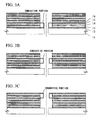
- Figs. 3A to 3C show examples of changing displays of three labels provided on the multi information recording medium.
- the layers sandwiched by a pair of the transparent electrodes function as a label.
- the labels are changed arbitrarily by selecting the transparent electrode that corresponds to one of the labels.
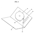
- FIG. 4 shows an example of a storing case that stores the above-described medium.
- a storing part 40 with a shallow dent shape capable of storing a disc 41 is provided in a storing case 42, and selecting means 43 for selecting the labels is attached thereto.
- the medium 41 and the storing case 42 are provided with marks 44 for alignment.
- the medium 41 is stored in the storing case such that the mark on the medium 41 is aligned with the mark provided on the storing case.
- the storing case is provided with a lid 45 which opens and closes freely for covering the storing part 40.
- Figs. 5A to 5C show examples of a method of changing the labels to be displayed.
- a label button 51 when a label button 51 is pressed, a voltage is applied to a corresponding pair of the electrodes in the multi information recording medium, and a label 52 recorded in advance on relevant layers is displayed.
- a label button 53 when a label button 53 is pressed, a voltage is applied to another pair of the electrodes, whereby a label 54 recorded on relevant layers is displayed similarly.
- Fig. 5C when a label button 55 is pressed, a voltage is applied to still another pair of the electrodes, whereby a different label 56 recorded on relevant layers is displayed similarly.
- Fig. 6 shows a layout example of the buttons constituting the label selecting means and the electrode portions on the inner periphery of the disc.
- Terminals 61 for applying voltage are provided on the storing case, the terminal 61 corresponding to positions of terminals to be connected to the transparent electrodes on the inner periphery of the disc, so that the transparent electrode area of the disc is connected to the terminals for applying voltage on the storing case.
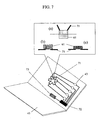
- Fig. 7 is a wiring diagram of the buttons and the terminals 61 for applying voltage.
- the terminals for applying voltage on the storing case indicated in Fig. 7 is made of a soft material which is deformed flexibly in a thickness direction so as to match the difference of height between the transparent electrodes on the disc.
- the terminal is, for example, a zebra connector which is formed by stacking soft material sheets and conductive materials alternately.
- the terminal 61 for applying voltage changes as shown in schematic cross-sectional views (b) and (c)
- the terminal 61 is still electrically conductive irrespective of the change in the thickness.
- the storing case is provided with a voltage source 73 such as a battery, voltage supplying means 72 having a function to divide voltage received from the voltage source 73 and to supply the voltage to selected wiring lines 71, and the wiring lines 71 connecting the label selecting means 43 to the terminals 61 for applying voltage.
- a battery small in size is used as the voltage source.
- a button-type small battery such as a lithium battery or an alkaline battery has electromotive force in a range from 1.5 V to 3.0 V, which is the sufficient voltage supply amount for label display. It is possible to produce the storing cases in various shapes by utilizing small and thin-profile characteristics. Moreover, it is possible to supply stable electric power without being influenced by brightness in a use environment.
- a small coin-shaped lithium battery having a diameter of 10 mm, a height of 2.5 mm, and a weight of 0.7 g is used in this embodiment.
- a voltage of the battery is set to 3 V, and a nominal capacity thereof is set to 30 mAh.
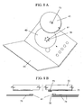
- Fig. 8A is a view showing a cross section of the disc and a cross section of the storing case when the voltage source is attached to the disc.
- the voltage source 73 is disposed at an inner peripheral portion of the disc. It is possible to supply the voltage by setting the disc on the storing case.
- a voltage receiver 76 is preferably formed into a flat spring and rendered flexible in the height direction so that the receiver is securely connected to the voltage source 73 or a terminal connected thereto.
- the transparent electrodes inside the disc do not always have to contact the terminals for applying voltage on the storing case as long as the a voltage is conductive therebetween.
- IrSnO x these materials can also be used as protective layers.
- IrSnO x it is possible to use other oxidized form electrochromic materials including NiOOH, CoOOH, tungsten oxalic acid complex, and organics such as heptylviologen.
- the solid electrolyte has a structure formed by sandwiching any of the following laminated films between transparent or semitransparent electrodes: WO 3 -Ta 2 O 5 -IrO x , WO 3 -Cr 2 O 3 , WO 3 -MgF 2 , WO 3 -RbAg 4 I 5 , WO 3 -SiO, WO 3 -ZrO 2 , WO 3 -LiClO 4 , WO 3 -LiF, WO 3 -Na 3 Zr 2 Si 2 PO 12 (NASICON), WO 3 -NaYSi 4 O 12 , and the like. It is also possible to replace part of or all of WO 3 in these materials with the above-mentioned other inorganic electrochromic materials such as MoO 3 .
- the electrochromic materials it is possible to use other materials which are not currently referred to as electrochromic materials as long as an absorption or reflection spectrum changes in such materials by voltage application. It is possible to form a small disc or a small recording medium even made of a single crystal. It should be noted, however, that, it is preferable to use a material having light absorption equal to or below 10% or more preferably equal to or below 5% in a low-absorption state.
- EL electroluminescent
- a photochromic material it is also possible to use a material obtained by blending an electroluminescent (EL) material with a photochromic material. The color of the photochromic material is allowed to change by light emitted from the EL material so as to cause light absorption relative to the wavelength of recording or reading light. It is possible to use an inorganic material such as ZnO as the EL material.
- the material of the transparent electrodes it is possible to use a publicly-known transparent electrode material adopting a composition of (In 2 O 3 ) x (SnO 2 ) 1-x , in which x is set in a range from 5% to 99% or more preferably in a range from 90% to 98% in terms of a resistance value. It is also possible to use other publicly-known material obtained by adding SiO 2 in an amount not exceeding 50 mol% to the above-described material or material obtained by adding 2 mol% to 5 mol% of another oxide such as Sb 2 O 3 to the SnO 2 in the above-described composition, for example.
- the adiabatic layer may be conductive, it is preferable to eliminate such conductivity.
- ZnS-SiO 2 can be used in this case.
- writing data used by a disc tester are formed by converting x-y coordinate positions of respective pixels to inverse polar coordinates on a personal computer.
- the writing data include information on pixels in one round of each disc on a radius of the disc basis.
- the size of one pixel on a disc label corresponds to a spot size of a laser. It is by all means possible to form one pixel by use of multiple laser spots.
- the size of laser spot and the size of label area determine specifications of the required image data.
- the bitmap (bmp) file including image data equivalent to 1800 x 1800 pixels is used in order to produce a label on the disc substrate having a diameter of 12 cm by use of laser spots each having a size of 50 ⁇ m.
- a comma separated value (csv) file indicating RGB values of the respective pixels is made from this bmp file to execute inverse polar coordinate calculation.
- the file after the inverse polar coordinate conversion is in conformity with r ⁇ expression.
- the writing data are produced based on the data thus obtained.
- the label is produced by performing irradiation of laser onto an electrochromic film on which a label layer is to be formed.
- a laser having a wavelength of 660 nm and numerical aperture (NA) of 0.65 is applied.
- NA numerical aperture
- an obtained contrast ratio of optical reflectivity of the recorded area to that of the unrecorded area is approximately equal to 2:1.
- a zoned constant linear velocity (ZCAV) method is used as a method of controlling a mortor at the time of recording and reproducing the information.
- ZCAV zoned constant linear velocity
- the rotation speed of the disc is changed at each zone where recording and reproducing are performed.
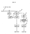
- every 8-bit data is defined as one unit, and the data are transferred to an 8-16 modulator 88.
- a modulation method of converting 8-bit information into 16-bit information is applied. This method is a so-called 8-16 modulation method.
- each piece of information having a mark length ranging from 3 T to 14 T that corresponds to the 8-bit information is recorded on the medium.
- the 8-16 modulator 88 in the diagram performs this modulation.
- the T represents a clock cycle at the time of recording the information.
- the disc is rotated such that a relative velocity to light spots becomes a linear velocity equal to 1 5 m/s.
- Digital signals each having the length ranging from 3 T to 14 T which are obtained by conversion by the 8-16 modulator 88 are transferred to a record wave pattern outbreak circuit 86, and a multi-pulse recording waveform is generated.
- the record wave pattern outbreak circuit includes a multi-pulse waveform table which is corresponding to a method referred to as control of adaptive recording waveform.
- the head pulse width and the end pulse width of the multi-pulse waveform are changed in response to lengths of space portions in front and back of mark portions at the time of forming a series of high-power pulse sequences for forming the mark portions.
- the record wave pattern outbreak circuit generates the multi-pulse recording waveform that can minimize the influence of heat interference being generated between the marks.
- the recording waveform generated by the record wave pattern outbreak circuit 86 is transferred to a laser drive circuit 87, and the laser drive circuit 87 causes a semiconductor laser in an optical head 83 to emit light based on this recording waveform.
- the rest of the layers not used as the label may be formed into either a write-once type or a rewritable type that can record information, into a read-only memory (ROM) type in which information is recorded in advance, or into a mixture of those types. Meanwhile, it is also possible to combine label information and recording information on the same layer instead of providing a layer used for label display and a layer used for recording information separately.
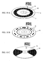
- Figs. 10A to 10C show examples of information recording areas 91 and label areas 92 being mixed on the same layer. These areas are separately arranged in a radial direction, in a circumferential direction or at random. In any case, the sizes of these areas may be defined arbitrarily.
- FIG. 10A shows an example of a medium in which the information recording areas 91 and the label area 92 are separated in the radial direction.
- Fig. 10C shows an example of a medium in which the information recording areas 91 and the label areas 92 are separated in the circumferential direction.
- Fig. 10B shows an example of a medium in which the information recording areas 91 and the label areas 92 are randomly mixed.
- FIGs. 11A and 11B show layout examples of storing cases in each of which a solar battery (photovoltaic [PV] cell) 77 is used as a voltage source.
- a solar battery photovoltaic [PV] cell
- a typical PV cell utilizes a light electromotive force effect of semiconductor.
- the light electromotive force effect is caused by two factors, namely, a photoconduction effect and a drift effect.
- a photoconduction effect When light is irradiated on the semiconductor, electrons and positive holes are excited at a conductor and a charging electron band owing to transition between bands or transition between band and level. Conductivity is increased as the electrons and the positive holes behave as free carriers. If there is an inner electric field in this situation, the drift effect is activated, and the electromotive force is generated by polarization of generation carriers. Therefore, in the light electromotive force effect, it is essential that light having sufficient energy for generating electron and positive hole pairs be incident, and that points of generation of such electron and positive hole pairs be located in the vicinity of junctions.
- the energy required for generating the electron and positive hole pairs corresponds to energy of light having a wavelength equal to or below 1 ⁇ m.
- Light from a fluorescent lamp used as a light source indoors has a wavelength in a range from 450 nm to 650 nm. Therefore, it is possible to obtain the voltage by use of the solar battery indoors.
- Fig. 11 shows an example of using the solar battery 77 that has specifications of a size of 62x83 mm, a voltage of 2 V, and a current of 250 mA. It is possible to expand the area of silicon cell by increasing the size of the solar battery, and thereby to increase both of the voltage and the current. Alternatively, by connecting multiple solar batteries in the same size in series or parallel, it is possible to acquire larger amounts of voltage and current than those of the single solar battery. Nevertheless, the single solar battery having a size of 62x83 mm is used in this embodiment considering the size of the optical disc.
- a voltage of 2 V corresponds to the rating voltage at the time of full output (when the load resistance is infinitely large) while a current of 250 mA corresponds to the maximum current applicable at the time of a short circuit (when the load resistance is equal to 0 ⁇ ).
- the voltage is equal to 1.3 V when the indoor fluorescent lamp is used.
- the brilliance in this case is equal to 600 lux as a result of measurement with a luminometer.
- the solar battery 77 may be located inside the storing case as shown in Fig. 11A or may be located on the outside of the storing case such as on the front surface of a lid 45 as shown in Fig. 11B .
- the layout will be similar to that of Fig. 7 .
- a solar battery 73a with a battery 73b as represented by the nickel-cadmium battery as shown in Figs. 12A and 12B .
- the solar battery generates the electromotive force under the light source, the brightness of the light source may vary indoors or outdoors. While the electromotive force of the solar battery may fluctuate in this case, it is possible to maintain the electromotive force constant at the time of displaying labels by embedding the battery in the storing case in advance for accumulating the electromotive force that is generated by the solar battery.
- multi information recording medium label selecting means, label areas, labels, a recording method of recording information, and the like not described in this embodiment are as set forth in the first embodiment.
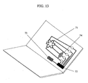
- Fig. 13 shows an example of displaying a multicolor label by selecting three layers simultaneously as the label layers described in the first and second embodiments.
- wiring lines are configured to apply a voltage simultaneously to three label layers when a label button 74 is pressed.
- the three label layers in this case are respectively made of different electrochromic materials selected so as to display mutually different colors by the layers.
- a WO 3 layer is used as the electrochromic layer in the film structure of a label A. In this way, the layer A exhibits a blue color upon voltage application.
- An Au-V 2 O 5 layer is used as the electrochromic layer in the film structure of a label B. In this way, the layer B exhibits a green color upon voltage application.
- a Cu-V 2 O 5 layer is used as the electrochromic layer in the film structure of a label C. In this way, the layer C exhibits a red color upon voltage application.
- the ratio of the label areas to the entire disc is increased by increasing the number of layers to be used as label layers, it is possible to display delicate colors by increasing the number of label layers, and therefore to achieve more beautiful label display. It is also possible to use additional three layers as label layers for displaying another label, or a single layer as an additional label layer may be used for displaying the subsequent label. Such combinations can be made freely.
- the number of the label layers may be increased up to 7 layers to obtain 7 colors, for example, for the purpose of forming more delicate color tones as a label image by increasing color tones. In this way, it is possible to obtain even more beautiful label display.
- Fig. 14 shows an example of using light as selecting means for the label layers described in the first to third embodiments.
- a remote controller 121 is provided herein for selecting the layer from outside, and the light is irradiated on a light-receiving portion 122. Usual infrared rays are used as the light source of the remote controller 121.
- label selecting means 43 on the remote controller a voltage is applied to the electrode corresponding to the label a to display the label a.
- a label b is selected with the remote controller
- a voltage is applied to the electrode corresponding to the label b to display the label b.
- the label c is displayed.
- buttons for selecting the layers inside the storing case since the changing of the labels can be performed with an optical switch. Therefore, it is possible to realize the storing case with a simple configuration.
- the storing case may be designed for a specific disc, and has a structure in which the label is displayed only when the disc matches the storing case.
- the positions of the transparent electrodes formed at the inner peripheral portion of the disc and the positions of the terminals for applying voltage formed on the storing case corresponding to the disc are located at the positions from those for other discs.
- Fig. 17A shows the layout of the different transparent electrodes formed at the inner peripheral portion of the disc shown in Fig. 2 in the first embodiment
- Figs. 17B and 17C show layout examples of the electrodes on the discs in this embodiment.
- the positions of the first transparent electrode and the second transparent electrode are aligned in the circumferential direction.
- Fig. 17B radial positions from the center of the disc are different between the first transparent electrodes and the second transparent electrodes. Accordingly, even when the disc Fig. 17B is stored in the storing case on which the electrodes are deposited as in the case of Fig. 17A , the label is not displayed because a voltage is not applied to the electrodes due to deviation of the positions of one of the electrodes. In the case of the disc shown in Fig. 17C , the radial positions and the circumferential positions are different between the first transparent electrodes and the second transparent electrodes. As a result, the label is not displayed, similarly. Fig. 17C also illustrates the layers constituting the electrodes. Here, only the electrode portions are required to be exposed on the surface.
- the disc is produced by stacking layers sequentially from the bottom by using appropriate masks to expose the electrode layers as illustrated in Fig. 17C .
- the label can be displayed and multiple labels can be changed to be displayed only when the positions between the terminals connected to the transparent electrodes of the disc the terminals for applying voltage on the storing case are fitted to each other.
- the present invention it is possible to obtain the information recording medium and the storing case of a collection type, which place importance on originality.
- the storing case may be provided with a dedicated label as well.
- the storing case has a configuration as illustrated in Fig. 18 .
- This storing case includes a label 161 formed on the case, electrodes 162 for the label layers on the storing case, terminals 61 for applying voltage, voltage source 73, voltage supplying means 72, label selecting means 43, and wiring lines 71 for connecting these constituents.
- Fig. 18 shows an example of using a small battery as a voltage source.
- Fig. 19 shows an example of using a solar battery
- Fig. 20 shows an example of using a solar battery and a battery.
- Label information is recorded in advance on the label layers on the storing case.
- the storing case is configured to display the label thereon only when a dedicated disc is set on, and a voltage is applied to the electrodes. Since the recording of the label information in this case is not performed on the disc, the recording is performed by converting the recorded positions into x-y coordinate information instead of performing the recording by rotation. It is more impressive to display labels on the disc and the storing case at the same time by arranging the label display in combination of the two. Of course, it is possible to select to display the labels only on the storing case or to display the labels only on the disc.
- the label layers provided on the storing case may have the same configuration as those on the disc. Alternatively, it is possible to adopt the combination with electronic paper used as the label.
- the electronic paper requires electric power for image display only when the label display is changed, and therefore has an advantage of low power consumption (refer to: http://jp.fujitsu.com/group/labs/techinfo/techguide/list/paper.html).
- Concerning the label selection a color on a layer sandwiched by two transparent electrodes is displayed as in the case of the disk of the voltage-selection-type. Liquid crystal layers corresponding to red, green, and blue may be selected at the same time to realize a full-color label.
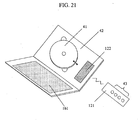
- the method of changing the labels as shown in Fig. 21 , it is possible to change the labels by transmitting the signal for information on labels recorded in advance to a light-receiving portion 122 by use of light such as infrared rays.
Landscapes
- Engineering & Computer Science (AREA)
- Mechanical Engineering (AREA)
- Optical Record Carriers And Manufacture Thereof (AREA)
- Optical Recording Or Reproduction (AREA)
- Packaging For Recording Disks (AREA)
Claims (10)
- Aufbewahrungsbehälter mit einem Aufbewahrungsteil (40) zum Aufbewahren eines Informationsaufzeichnungsmediums (41), das eine Informationsaufzeichnungsfläche (91) zum Aufzeichnen von Information durch Bestrahlung mit Energie und mehrere Kennzeichnungsflächen (92) zum Aufzeichnen sichtbarer Kennzeichnungsinformation aufweist,
wobei das Informationsaufzeichnungsmedium (41) ferner mehrere Elektrodenanschlüsse aufweist, die jeweils an die mehreren Kennzeichnungsflächen (92) angeschlossen sind, wobei eine in jede der Kennzeichnungsflächen geschriebene Kennzeichnung sichtbar angezeigt wird, wenn eine Spannung von den Elektrodenanschlüssen an die jeweilige Kennzeichnungsfläche angelegt wird,
dadurch gekennzeichnet, daß der Aufbewahrungsbehälter (42) ferner Spannungsversorgungsanschlüsse (61), die an Positionen angeordnet sind, um mit den Elektrodenanschlüssen des in dem Aufbewahrungsteil (40) aufbewahrten Informationsaufzeichnungsmediums (41) verbunden zu werden, eine Auswahleinrichtung (43) zum Auswählen des Spannungsversorgungsanschlusses (61), und eine Leistungsquelle (73) zum Anlegen einer Spannung an den ausgewählten Spannungsversorgungsanschluss (61), aufweist. - Aufbewahrungsbehälter nach Anspruch 1, wobei die Auswahleinrichtung (43) einen Modus aufweist, um mehrere Spannungsversorgungsanschlüsse (61) gleichzeitig auszuwählen.
- Informationsaufzeichnungsmediums-Aufbewahrungssystem mit
einem Informationsaufzeichnungsmedium (41), das eine Informationsaufzeichnugnsfläche (91) zum Aufzeichnen von Information durch Bestrahlung mit Energie und mehrere Kennzeichnungsflächen (92) zum Aufzeichnen sichtbarer Kennzeichnungsinformation aufweist, und
einem Aufbewahrungsbehälter (42) mit einem Aufbewahrungsteil (40), der das Informationsaufzeichnungsmedium (41) aufbewahrt,
dadurch gekennzeichnet, daß
das Informationsaufzeichnungsmedium (41) ferner mehrere Elektrodenanschlüsse aufweist, die jeweils an die mehreren Kennzeichnungsflächen (92) angeschlossen sind, und das Informationsaufzeichnungsmedium (41) dazu ausgelegt ist, eine in jede der Kennzeichnungsflächen geschriebene Kennzeichnung sichtbar anzuzeigen, wenn eine Spannung von den Elektrodenanschlüssen an die jeweilige Kennzeichnungsfläche (92) angelegt wird, und
der Aufbewahrungsbehälter (42) ferner Spannungsversorgungsanschlüsse (61), die an Positionen angeordnet sind, um mit den Elektrodenanschlüssen des in dem Aufbewahrungsteil (40) aufbewahrten Informationsaufzeichnungsmedium verbunden zu werden, eine Auswahleinrichtung (43) zum Auswählen der Spannungsversorgungsanschlüsse (61) und eine Leistungsquelle (73) zum Anlegen einer Spannung an den ausgewählten Spannungsversorgungsanschluss (61), aufweist. - Behälter nach Anspruch 1 oder System nach Anspruch 3, wobei
das Informationsaufzeichnungsmedium (41) ein Mehrschichtmedium ist, das mehrere Aufzeichnungsschichten aufweist, und
die mehreren Kennzeichnungsflächen (92) jeweils den Aufzeichnungsschichten entsprechen. - System nach Anspruch 4, wobei jede der Aufzeichnungsschichten eine elektrochrome Schicht (13, 15) aufweist, die zwischen einem Paar von transparenten Elektroden (12, 16) liegt.
- System nach Anspruch 5, wobei
die mehreren Kennzeichnungsflächen (92) jeweils mehrere Aufzeichnungsschichten zum Anzeigen wechselseitig verschiedener Farben aufweisen, und
die Auswahleinrichtung (43) einen Modus aufweist, um mehrere Spannungsversorgungsanschlüsse (61) auszuwählen, die den mehreren Aufzeichnungsschichten zum Anzeigen wechselseitig verschiedener Farben entsprechen. - Behälter nach Anspruch 1 oder System nach Anspruch 3, wobei die Leistungsquelle (73) eine Solarbatterie und eine Batterie aufweist.
- Behälter nach Anspruch 1 oder System nach Anspruch 3, ferner mit einem Aufnahmeteil zum Aufnehmen eines Fernsteuerungssignals,
wobei die Auswahleinrichtung (43) die Spannungsversorgungsanschlüsse (61) auf Grundlage des von dem Empfangsteil empfangenen Fernsteuerungssignals auswählt. - Behälter nach Anspruch 1 oder System nach Anspruch 3, ferner mit einem Deckelelement (45), das sich frei öffnen und schließen läßt, um den Aufnahmeteil (40) zu überdecken,
wobei das Deckelelement (45) einen Fensterabschnitt aufweist, durch den wenigstens ein Teil des in dem Aufbewahrungsteil (40) aufbewahrten Informationsaufzeichnungsmediums (41) sichtbar ist. - Behälter nach Anspruch 1 oder System nach Anspruch 3, ferner mit einem Deckelelement (45), das sich frei öffnen und schließen läßt, um den Aufnahmeteil (40) zu überdecken,
wobei das Deckelelement (45) eine Kennzeichnungsschicht aufweist, um die Kennzeichnungsinformation aufzuzeichnen, und um die Kennzeichnungsinformation sichtbar anzuzeigen, wenn über die Auswahleinrichtung (43) eine Spannung an das Deckelelement angelegt ist, und
wobei die Kennzeichnungsschicht vorzugsweise elektronisches Papier ist.
Applications Claiming Priority (1)
| Application Number | Priority Date | Filing Date | Title |
|---|---|---|---|
| JP2006160028A JP2007328872A (ja) | 2006-06-08 | 2006-06-08 | 情報記録媒体収納システム及び収納ケース |
Publications (2)
| Publication Number | Publication Date |
|---|---|
| EP1865511A1 EP1865511A1 (de) | 2007-12-12 |
| EP1865511B1 true EP1865511B1 (de) | 2009-12-09 |
Family
ID=38474004
Family Applications (1)
| Application Number | Title | Priority Date | Filing Date |
|---|---|---|---|
| EP07007090A Expired - Fee Related EP1865511B1 (de) | 2006-06-08 | 2007-04-04 | Aufbewahrungssystem und Aufbewahrungsbehälter für ein Informationsaufzeichnungsmedium |
Country Status (6)
| Country | Link |
|---|---|
| US (1) | US7852740B2 (de) |
| EP (1) | EP1865511B1 (de) |
| JP (1) | JP2007328872A (de) |
| KR (1) | KR100858394B1 (de) |
| CN (1) | CN100590729C (de) |
| DE (1) | DE602007003637D1 (de) |
Families Citing this family (2)
| Publication number | Priority date | Publication date | Assignee | Title |
|---|---|---|---|---|
| JPWO2006126640A1 (ja) * | 2005-05-25 | 2008-12-25 | 松下電器産業株式会社 | ディスク装置 |
| US8234667B2 (en) * | 2008-01-04 | 2012-07-31 | International Business Machines Corporation | Disk with embedded flash memory and disc drive |
Family Cites Families (20)
| Publication number | Priority date | Publication date | Assignee | Title |
|---|---|---|---|---|
| JP3417104B2 (ja) * | 1994-12-07 | 2003-06-16 | ソニー株式会社 | 記録媒体、収納ケースおよび記録再生装置 |
| FR2759881B1 (fr) | 1997-02-26 | 1999-04-23 | Fors France Sa | Equipement de presentation sur le lieu de vente de supports d'enregistrement audiovisuels, boitiers d'emballage et boitiers antivols mis en oeuvre |
| DE19857315A1 (de) | 1997-12-12 | 1999-08-05 | Ricoh Kk | Optisches Informationsspeichermaterial und Anzeige-Aufzeichnungsverfahren unter Verwendung desselben |
| JP4322337B2 (ja) * | 1998-12-28 | 2009-08-26 | 株式会社東芝 | 記録用カセットの情報記録装置 |
| JP2001283470A (ja) * | 2000-03-31 | 2001-10-12 | Pioneer Electronic Corp | 情報記録システム及び情報記録方法 |
| JP3577005B2 (ja) | 2001-06-27 | 2004-10-13 | 株式会社日立製作所 | 図形書き込み方法 |
| JP2003242750A (ja) | 2002-02-15 | 2003-08-29 | Yamaha Corp | ディスクおよび感熱層部材 |
| JP2003331560A (ja) | 2002-05-14 | 2003-11-21 | Sony Corp | 記録媒体および記録媒体記録再生装置 |
| JP4120268B2 (ja) | 2002-05-27 | 2008-07-16 | 株式会社日立製作所 | 情報記録媒体および情報記録方法 |
| JP2004310912A (ja) * | 2003-04-08 | 2004-11-04 | Hitachi Ltd | 情報記録方法および情報記録装置 |
| EP1500601A1 (de) * | 2003-07-25 | 2005-01-26 | Amcor Flexibles Europe A/S | Wiederverschliessbarer Verpackungsbeutel sowie Verfahren zu seiner Herstellung |
| US20070121190A1 (en) * | 2003-10-21 | 2007-05-31 | Koninklijke Philips Electronics N.V. | Display |
| JP2005235359A (ja) | 2004-03-26 | 2005-09-02 | Kazuhiro Yamamoto | レーベル面印刷可能な外部記憶メディア用ドライブ、メディア、プログラムおよび端末装置 |
| JP2005285201A (ja) | 2004-03-29 | 2005-10-13 | Sharp Corp | 記録媒体および記録再生装置 |
| US7639271B2 (en) | 2004-04-30 | 2009-12-29 | Hewlett-Packard Development Company, L.P. | Labeling an optical disc |
| US7317396B2 (en) * | 2004-05-26 | 2008-01-08 | Funai Electric Co., Ltd. | Optical disc having RFID tag, optical disc apparatus, and system for preventing unauthorized copying |
| JP2006228358A (ja) | 2005-02-21 | 2006-08-31 | Hitachi Maxell Ltd | 情報記録媒体およびその製造方法 |
| US20050276211A1 (en) * | 2004-06-09 | 2005-12-15 | Akemi Hirotsune | Information recording medium and manufacturing process |
| JP2005350093A (ja) | 2004-06-09 | 2005-12-22 | Canon Inc | ディスクケース及び該ディスクケースを用いる記録装置 |
| JP4408106B2 (ja) * | 2005-04-14 | 2010-02-03 | 日立マクセル株式会社 | スタンパ |
-
2006
- 2006-06-08 JP JP2006160028A patent/JP2007328872A/ja active Pending
-
2007
- 2007-02-27 CN CN200710084825A patent/CN100590729C/zh not_active Expired - Fee Related
- 2007-02-27 KR KR1020070019302A patent/KR100858394B1/ko not_active Expired - Fee Related
- 2007-04-04 US US11/696,284 patent/US7852740B2/en not_active Expired - Fee Related
- 2007-04-04 EP EP07007090A patent/EP1865511B1/de not_active Expired - Fee Related
- 2007-04-04 DE DE602007003637T patent/DE602007003637D1/de active Active
Also Published As
| Publication number | Publication date |
|---|---|
| EP1865511A1 (de) | 2007-12-12 |
| US7852740B2 (en) | 2010-12-14 |
| KR100858394B1 (ko) | 2008-09-11 |
| CN100590729C (zh) | 2010-02-17 |
| KR20070117444A (ko) | 2007-12-12 |
| JP2007328872A (ja) | 2007-12-20 |
| DE602007003637D1 (de) | 2010-01-21 |
| CN101086890A (zh) | 2007-12-12 |
| US20070284271A1 (en) | 2007-12-13 |
Similar Documents
| Publication | Publication Date | Title |
|---|---|---|
| US6473058B1 (en) | Information display device and display control method | |
| US7116309B1 (en) | Photowriting display device and photowriting display unit incorporating the same | |
| JP4513414B2 (ja) | 画像表示装置 | |
| JP5287263B2 (ja) | 表示装置、及び、表示装置の制御方法 | |
| EP1865511B1 (de) | Aufbewahrungssystem und Aufbewahrungsbehälter für ein Informationsaufzeichnungsmedium | |
| JP2005321911A (ja) | 発光素子付き透明icカード | |
| US20150098120A1 (en) | Interferometric-modulator-based reflective labels and tags and methods for their manufacture | |
| CN101064125B (zh) | 光盘及向光盘写入可识别的图形的方法 | |
| JP2007510939A (ja) | ディスプレイ | |
| JP2010286992A (ja) | 書込装置及び画像表示システム | |
| US12332511B2 (en) | Method of forming a pattern on an optical device | |
| US7935404B2 (en) | System and method for marking an optical disk | |
| KR19980064523A (ko) | 발광부를 가지는 정보기록매체, 정보기록매체용 수납케이스, 및정보기록매체용 시트 | |
| JP2004203026A (ja) | 可逆性多色記録層を有するシート材、カード、及びこれらを用いた記録方法 | |
| JPH11291675A (ja) | リライトカード | |
| JPH0827691B2 (ja) | 情報処理装置 | |
| JPH10161160A (ja) | 記録用シート及び記録装置 | |
| JPS60225229A (ja) | 電子機器 | |
| JPH0439744B2 (de) | ||
| WO2007052795A1 (ja) | 記憶装置 | |
| JPS60225241A (ja) | 電子機器 | |
| JPS60225228A (ja) | 電子機器 | |
| JP2010231030A (ja) | 表示装置及び表示媒体 | |
| JPS60225242A (ja) | 電子機器 | |
| JPS62127895A (ja) | エレクトロルミネツセントパネルの駆動装置 |
Legal Events
| Date | Code | Title | Description |
|---|---|---|---|
| PUAI | Public reference made under article 153(3) epc to a published international application that has entered the european phase |
Free format text: ORIGINAL CODE: 0009012 |
|
| AK | Designated contracting states |
Kind code of ref document: A1 Designated state(s): AT BE BG CH CY CZ DE DK EE ES FI FR GB GR HU IE IS IT LI LT LU LV MC MT NL PL PT RO SE SI SK TR |
|
| AX | Request for extension of the european patent |
Extension state: AL BA HR MK YU |
|
| 17P | Request for examination filed |
Effective date: 20080331 |
|
| 17Q | First examination report despatched |
Effective date: 20080508 |
|
| AKX | Designation fees paid |
Designated state(s): DE FR GB |
|
| GRAP | Despatch of communication of intention to grant a patent |
Free format text: ORIGINAL CODE: EPIDOSNIGR1 |
|
| RIN1 | Information on inventor provided before grant (corrected) |
Inventor name: HOSHINO, TAKESHI Inventor name: OTSUKA, RIEKO Inventor name: SUKEDA, HIROKO Inventor name: HORII, YOUICHI Inventor name: MUKOH, MASAKI Inventor name: HIROTSUNE, AKEMI Inventor name: ANZAI, YUMIKO |
|
| GRAS | Grant fee paid |
Free format text: ORIGINAL CODE: EPIDOSNIGR3 |
|
| GRAA | (expected) grant |
Free format text: ORIGINAL CODE: 0009210 |
|
| AK | Designated contracting states |
Kind code of ref document: B1 Designated state(s): DE FR GB |
|
| REG | Reference to a national code |
Ref country code: GB Ref legal event code: FG4D |
|
| REF | Corresponds to: |
Ref document number: 602007003637 Country of ref document: DE Date of ref document: 20100121 Kind code of ref document: P |
|
| PGFP | Annual fee paid to national office [announced via postgrant information from national office to epo] |
Ref country code: FR Payment date: 20100416 Year of fee payment: 4 |
|
| PGFP | Annual fee paid to national office [announced via postgrant information from national office to epo] |
Ref country code: DE Payment date: 20100622 Year of fee payment: 4 |
|
| PLBE | No opposition filed within time limit |
Free format text: ORIGINAL CODE: 0009261 |
|
| STAA | Information on the status of an ep patent application or granted ep patent |
Free format text: STATUS: NO OPPOSITION FILED WITHIN TIME LIMIT |
|
| 26N | No opposition filed |
Effective date: 20100910 |
|
| GBPC | Gb: european patent ceased through non-payment of renewal fee |
Effective date: 20110404 |
|
| REG | Reference to a national code |
Ref country code: FR Ref legal event code: ST Effective date: 20111230 |
|
| PG25 | Lapsed in a contracting state [announced via postgrant information from national office to epo] |
Ref country code: DE Free format text: LAPSE BECAUSE OF NON-PAYMENT OF DUE FEES Effective date: 20111101 Ref country code: FR Free format text: LAPSE BECAUSE OF NON-PAYMENT OF DUE FEES Effective date: 20110502 |
|
| PG25 | Lapsed in a contracting state [announced via postgrant information from national office to epo] |
Ref country code: GB Free format text: LAPSE BECAUSE OF NON-PAYMENT OF DUE FEES Effective date: 20110404 |
|
| REG | Reference to a national code |
Ref country code: DE Ref legal event code: R119 Ref document number: 602007003637 Country of ref document: DE Effective date: 20111101 |