EP1863092A2 - Speichervorrichtung, insbesondere Phasenwechselspeicher mit wahlfreiem Zugriff, mit Nanodraht-Transistor und Verfahren zur Herstellung der Speichervorrichtung - Google Patents
Speichervorrichtung, insbesondere Phasenwechselspeicher mit wahlfreiem Zugriff, mit Nanodraht-Transistor und Verfahren zur Herstellung der Speichervorrichtung Download PDFInfo
- Publication number
- EP1863092A2 EP1863092A2 EP07008964A EP07008964A EP1863092A2 EP 1863092 A2 EP1863092 A2 EP 1863092A2 EP 07008964 A EP07008964 A EP 07008964A EP 07008964 A EP07008964 A EP 07008964A EP 1863092 A2 EP1863092 A2 EP 1863092A2
- Authority
- EP
- European Patent Office
- Prior art keywords
- memory device
- nanowire
- nanofibre
- nanotube
- transistor
- Prior art date
- Legal status (The legal status is an assumption and is not a legal conclusion. Google has not performed a legal analysis and makes no representation as to the accuracy of the status listed.)
- Withdrawn
Links
- 239000002070 nanowire Substances 0.000 title claims abstract description 58
- 238000000034 method Methods 0.000 title claims abstract description 38
- 230000008859 change Effects 0.000 title claims abstract description 29
- 239000002121 nanofiber Substances 0.000 claims abstract description 48
- 239000002071 nanotube Substances 0.000 claims abstract description 48
- 239000000463 material Substances 0.000 claims abstract description 35
- 239000011149 active material Substances 0.000 claims description 36
- 150000001875 compounds Chemical class 0.000 claims description 6
- -1 chalcogenide compound Chemical class 0.000 claims description 5
- 150000004770 chalcogenides Chemical class 0.000 claims description 4
- 230000015654 memory Effects 0.000 description 57
- VYPSYNLAJGMNEJ-UHFFFAOYSA-N Silicium dioxide Chemical compound O=[Si]=O VYPSYNLAJGMNEJ-UHFFFAOYSA-N 0.000 description 50
- 230000008569 process Effects 0.000 description 32
- 230000002093 peripheral effect Effects 0.000 description 29
- 229910052681 coesite Inorganic materials 0.000 description 25
- 229910052906 cristobalite Inorganic materials 0.000 description 25
- 239000000377 silicon dioxide Substances 0.000 description 25
- 229910052682 stishovite Inorganic materials 0.000 description 25
- 229910052905 tridymite Inorganic materials 0.000 description 25
- 229910052751 metal Inorganic materials 0.000 description 14
- 239000002184 metal Substances 0.000 description 14
- 238000010438 heat treatment Methods 0.000 description 13
- 239000010949 copper Substances 0.000 description 8
- 238000005530 etching Methods 0.000 description 7
- 230000004888 barrier function Effects 0.000 description 6
- 239000003054 catalyst Substances 0.000 description 6
- 238000000151 deposition Methods 0.000 description 6
- 239000000945 filler Substances 0.000 description 5
- 238000005498 polishing Methods 0.000 description 5
- 238000007517 polishing process Methods 0.000 description 5
- 238000005229 chemical vapour deposition Methods 0.000 description 4
- 238000002955 isolation Methods 0.000 description 4
- 239000000126 substance Substances 0.000 description 4
- 239000010936 titanium Substances 0.000 description 4
- PXHVJJICTQNCMI-UHFFFAOYSA-N Nickel Chemical compound [Ni] PXHVJJICTQNCMI-UHFFFAOYSA-N 0.000 description 3
- 229910052802 copper Inorganic materials 0.000 description 3
- 238000005137 deposition process Methods 0.000 description 3
- 238000005516 engineering process Methods 0.000 description 3
- 229910052719 titanium Inorganic materials 0.000 description 3
- 229910052721 tungsten Inorganic materials 0.000 description 3
- XUIMIQQOPSSXEZ-UHFFFAOYSA-N Silicon Chemical compound [Si] XUIMIQQOPSSXEZ-UHFFFAOYSA-N 0.000 description 2
- 238000000231 atomic layer deposition Methods 0.000 description 2
- 238000001816 cooling Methods 0.000 description 2
- 238000002425 crystallisation Methods 0.000 description 2
- 230000008025 crystallization Effects 0.000 description 2
- 230000006870 function Effects 0.000 description 2
- 229910052737 gold Inorganic materials 0.000 description 2
- 238000002844 melting Methods 0.000 description 2
- 230000008018 melting Effects 0.000 description 2
- 229910052759 nickel Inorganic materials 0.000 description 2
- 238000005240 physical vapour deposition Methods 0.000 description 2
- 239000002244 precipitate Substances 0.000 description 2
- 239000004065 semiconductor Substances 0.000 description 2
- 229910052710 silicon Inorganic materials 0.000 description 2
- 239000010703 silicon Substances 0.000 description 2
- 239000000758 substrate Substances 0.000 description 2
- 229910052715 tantalum Inorganic materials 0.000 description 2
- OKTJSMMVPCPJKN-UHFFFAOYSA-N Carbon Chemical compound [C] OKTJSMMVPCPJKN-UHFFFAOYSA-N 0.000 description 1
- RYGMFSIKBFXOCR-UHFFFAOYSA-N Copper Chemical compound [Cu] RYGMFSIKBFXOCR-UHFFFAOYSA-N 0.000 description 1
- 229910000618 GeSbTe Inorganic materials 0.000 description 1
- 229910005866 GeSe Inorganic materials 0.000 description 1
- 229910004200 TaSiN Inorganic materials 0.000 description 1
- 229910010037 TiAlN Inorganic materials 0.000 description 1
- 229910008482 TiSiN Inorganic materials 0.000 description 1
- ATJFFYVFTNAWJD-UHFFFAOYSA-N Tin Chemical compound [Sn] ATJFFYVFTNAWJD-UHFFFAOYSA-N 0.000 description 1
- RTAQQCXQSZGOHL-UHFFFAOYSA-N Titanium Chemical compound [Ti] RTAQQCXQSZGOHL-UHFFFAOYSA-N 0.000 description 1
- 230000003213 activating effect Effects 0.000 description 1
- 230000006978 adaptation Effects 0.000 description 1
- 229910052799 carbon Inorganic materials 0.000 description 1
- 229910052804 chromium Inorganic materials 0.000 description 1
- 230000015271 coagulation Effects 0.000 description 1
- 238000005345 coagulation Methods 0.000 description 1
- 229910017052 cobalt Inorganic materials 0.000 description 1
- 239000010941 cobalt Substances 0.000 description 1
- GUTLYIVDDKVIGB-UHFFFAOYSA-N cobalt atom Chemical compound [Co] GUTLYIVDDKVIGB-UHFFFAOYSA-N 0.000 description 1
- 230000002708 enhancing effect Effects 0.000 description 1
- 238000011156 evaluation Methods 0.000 description 1
- 239000007789 gas Substances 0.000 description 1
- 239000011521 glass Substances 0.000 description 1
- 239000010931 gold Substances 0.000 description 1
- 229910052735 hafnium Inorganic materials 0.000 description 1
- 230000010354 integration Effects 0.000 description 1
- 229910052741 iridium Inorganic materials 0.000 description 1
- QRXWMOHMRWLFEY-UHFFFAOYSA-N isoniazide Chemical compound NNC(=O)C1=CC=NC=C1 QRXWMOHMRWLFEY-UHFFFAOYSA-N 0.000 description 1
- 229910052748 manganese Inorganic materials 0.000 description 1
- 230000007246 mechanism Effects 0.000 description 1
- 229910052750 molybdenum Inorganic materials 0.000 description 1
- 230000003287 optical effect Effects 0.000 description 1
- 229910052763 palladium Inorganic materials 0.000 description 1
- KDLHZDBZIXYQEI-UHFFFAOYSA-N palladium Substances [Pd] KDLHZDBZIXYQEI-UHFFFAOYSA-N 0.000 description 1
- 238000007747 plating Methods 0.000 description 1
- 229910052697 platinum Inorganic materials 0.000 description 1
- BASFCYQUMIYNBI-UHFFFAOYSA-N platinum Substances [Pt] BASFCYQUMIYNBI-UHFFFAOYSA-N 0.000 description 1
- 229920000747 poly(lactic acid) Polymers 0.000 description 1
- 229910052703 rhodium Inorganic materials 0.000 description 1
- 229910021332 silicide Inorganic materials 0.000 description 1
- FVBUAEGBCNSCDD-UHFFFAOYSA-N silicide(4-) Chemical compound [Si-4] FVBUAEGBCNSCDD-UHFFFAOYSA-N 0.000 description 1
- 229910052709 silver Inorganic materials 0.000 description 1
- 239000007787 solid Substances 0.000 description 1
- 238000004544 sputter deposition Methods 0.000 description 1
- 230000003068 static effect Effects 0.000 description 1
- WFKWXMTUELFFGS-UHFFFAOYSA-N tungsten Chemical compound [W] WFKWXMTUELFFGS-UHFFFAOYSA-N 0.000 description 1
- 239000010937 tungsten Substances 0.000 description 1
- 229910052725 zinc Inorganic materials 0.000 description 1
- 229910052726 zirconium Inorganic materials 0.000 description 1
Images











Classifications
-
- H—ELECTRICITY
- H10—SEMICONDUCTOR DEVICES; ELECTRIC SOLID-STATE DEVICES NOT OTHERWISE PROVIDED FOR
- H10N—ELECTRIC SOLID-STATE DEVICES NOT OTHERWISE PROVIDED FOR
- H10N70/00—Solid-state devices having no potential barriers, and specially adapted for rectifying, amplifying, oscillating or switching
- H10N70/20—Multistable switching devices, e.g. memristors
- H10N70/231—Multistable switching devices, e.g. memristors based on solid-state phase change, e.g. between amorphous and crystalline phases, Ovshinsky effect
-
- G—PHYSICS
- G11—INFORMATION STORAGE
- G11C—STATIC STORES
- G11C13/00—Digital stores characterised by the use of storage elements not covered by groups G11C11/00, G11C23/00, or G11C25/00
- G11C13/0002—Digital stores characterised by the use of storage elements not covered by groups G11C11/00, G11C23/00, or G11C25/00 using resistive RAM [RRAM] elements
- G11C13/0004—Digital stores characterised by the use of storage elements not covered by groups G11C11/00, G11C23/00, or G11C25/00 using resistive RAM [RRAM] elements comprising amorphous/crystalline phase transition cells
-
- H—ELECTRICITY
- H10—SEMICONDUCTOR DEVICES; ELECTRIC SOLID-STATE DEVICES NOT OTHERWISE PROVIDED FOR
- H10B—ELECTRONIC MEMORY DEVICES
- H10B63/00—Resistance change memory devices, e.g. resistive RAM [ReRAM] devices
- H10B63/30—Resistance change memory devices, e.g. resistive RAM [ReRAM] devices comprising selection components having three or more electrodes, e.g. transistors
- H10B63/34—Resistance change memory devices, e.g. resistive RAM [ReRAM] devices comprising selection components having three or more electrodes, e.g. transistors of the vertical channel field-effect transistor type
-
- H—ELECTRICITY
- H10—SEMICONDUCTOR DEVICES; ELECTRIC SOLID-STATE DEVICES NOT OTHERWISE PROVIDED FOR
- H10B—ELECTRONIC MEMORY DEVICES
- H10B63/00—Resistance change memory devices, e.g. resistive RAM [ReRAM] devices
- H10B63/80—Arrangements comprising multiple bistable or multi-stable switching components of the same type on a plane parallel to the substrate, e.g. cross-point arrays
-
- H—ELECTRICITY
- H10—SEMICONDUCTOR DEVICES; ELECTRIC SOLID-STATE DEVICES NOT OTHERWISE PROVIDED FOR
- H10N—ELECTRIC SOLID-STATE DEVICES NOT OTHERWISE PROVIDED FOR
- H10N70/00—Solid-state devices having no potential barriers, and specially adapted for rectifying, amplifying, oscillating or switching
- H10N70/20—Multistable switching devices, e.g. memristors
- H10N70/24—Multistable switching devices, e.g. memristors based on migration or redistribution of ionic species, e.g. anions, vacancies
- H10N70/245—Multistable switching devices, e.g. memristors based on migration or redistribution of ionic species, e.g. anions, vacancies the species being metal cations, e.g. programmable metallization cells
-
- H—ELECTRICITY
- H10—SEMICONDUCTOR DEVICES; ELECTRIC SOLID-STATE DEVICES NOT OTHERWISE PROVIDED FOR
- H10N—ELECTRIC SOLID-STATE DEVICES NOT OTHERWISE PROVIDED FOR
- H10N70/00—Solid-state devices having no potential barriers, and specially adapted for rectifying, amplifying, oscillating or switching
- H10N70/801—Constructional details of multistable switching devices
- H10N70/821—Device geometry
- H10N70/826—Device geometry adapted for essentially vertical current flow, e.g. sandwich or pillar type devices
-
- H—ELECTRICITY
- H10—SEMICONDUCTOR DEVICES; ELECTRIC SOLID-STATE DEVICES NOT OTHERWISE PROVIDED FOR
- H10N—ELECTRIC SOLID-STATE DEVICES NOT OTHERWISE PROVIDED FOR
- H10N70/00—Solid-state devices having no potential barriers, and specially adapted for rectifying, amplifying, oscillating or switching
- H10N70/801—Constructional details of multistable switching devices
- H10N70/881—Switching materials
- H10N70/882—Compounds of sulfur, selenium or tellurium, e.g. chalcogenides
- H10N70/8822—Sulfides, e.g. CuS
-
- H—ELECTRICITY
- H10—SEMICONDUCTOR DEVICES; ELECTRIC SOLID-STATE DEVICES NOT OTHERWISE PROVIDED FOR
- H10N—ELECTRIC SOLID-STATE DEVICES NOT OTHERWISE PROVIDED FOR
- H10N70/00—Solid-state devices having no potential barriers, and specially adapted for rectifying, amplifying, oscillating or switching
- H10N70/801—Constructional details of multistable switching devices
- H10N70/881—Switching materials
- H10N70/882—Compounds of sulfur, selenium or tellurium, e.g. chalcogenides
- H10N70/8825—Selenides, e.g. GeSe
-
- H—ELECTRICITY
- H10—SEMICONDUCTOR DEVICES; ELECTRIC SOLID-STATE DEVICES NOT OTHERWISE PROVIDED FOR
- H10N—ELECTRIC SOLID-STATE DEVICES NOT OTHERWISE PROVIDED FOR
- H10N70/00—Solid-state devices having no potential barriers, and specially adapted for rectifying, amplifying, oscillating or switching
- H10N70/801—Constructional details of multistable switching devices
- H10N70/881—Switching materials
- H10N70/882—Compounds of sulfur, selenium or tellurium, e.g. chalcogenides
- H10N70/8828—Tellurides, e.g. GeSbTe
-
- Y—GENERAL TAGGING OF NEW TECHNOLOGICAL DEVELOPMENTS; GENERAL TAGGING OF CROSS-SECTIONAL TECHNOLOGIES SPANNING OVER SEVERAL SECTIONS OF THE IPC; TECHNICAL SUBJECTS COVERED BY FORMER USPC CROSS-REFERENCE ART COLLECTIONS [XRACs] AND DIGESTS
- Y10—TECHNICAL SUBJECTS COVERED BY FORMER USPC
- Y10S—TECHNICAL SUBJECTS COVERED BY FORMER USPC CROSS-REFERENCE ART COLLECTIONS [XRACs] AND DIGESTS
- Y10S977/00—Nanotechnology
- Y10S977/70—Nanostructure
- Y10S977/762—Nanowire or quantum wire, i.e. axially elongated structure having two dimensions of 100 nm or less
-
- Y—GENERAL TAGGING OF NEW TECHNOLOGICAL DEVELOPMENTS; GENERAL TAGGING OF CROSS-SECTIONAL TECHNOLOGIES SPANNING OVER SEVERAL SECTIONS OF THE IPC; TECHNICAL SUBJECTS COVERED BY FORMER USPC CROSS-REFERENCE ART COLLECTIONS [XRACs] AND DIGESTS
- Y10—TECHNICAL SUBJECTS COVERED BY FORMER USPC
- Y10S—TECHNICAL SUBJECTS COVERED BY FORMER USPC CROSS-REFERENCE ART COLLECTIONS [XRACs] AND DIGESTS
- Y10S977/00—Nanotechnology
- Y10S977/70—Nanostructure
- Y10S977/773—Nanoparticle, i.e. structure having three dimensions of 100 nm or less
-
- Y—GENERAL TAGGING OF NEW TECHNOLOGICAL DEVELOPMENTS; GENERAL TAGGING OF CROSS-SECTIONAL TECHNOLOGIES SPANNING OVER SEVERAL SECTIONS OF THE IPC; TECHNICAL SUBJECTS COVERED BY FORMER USPC CROSS-REFERENCE ART COLLECTIONS [XRACs] AND DIGESTS
- Y10—TECHNICAL SUBJECTS COVERED BY FORMER USPC
- Y10S—TECHNICAL SUBJECTS COVERED BY FORMER USPC CROSS-REFERENCE ART COLLECTIONS [XRACs] AND DIGESTS
- Y10S977/00—Nanotechnology
- Y10S977/902—Specified use of nanostructure
- Y10S977/932—Specified use of nanostructure for electronic or optoelectronic application
-
- Y—GENERAL TAGGING OF NEW TECHNOLOGICAL DEVELOPMENTS; GENERAL TAGGING OF CROSS-SECTIONAL TECHNOLOGIES SPANNING OVER SEVERAL SECTIONS OF THE IPC; TECHNICAL SUBJECTS COVERED BY FORMER USPC CROSS-REFERENCE ART COLLECTIONS [XRACs] AND DIGESTS
- Y10—TECHNICAL SUBJECTS COVERED BY FORMER USPC
- Y10S—TECHNICAL SUBJECTS COVERED BY FORMER USPC CROSS-REFERENCE ART COLLECTIONS [XRACs] AND DIGESTS
- Y10S977/00—Nanotechnology
- Y10S977/902—Specified use of nanostructure
- Y10S977/932—Specified use of nanostructure for electronic or optoelectronic application
- Y10S977/936—Specified use of nanostructure for electronic or optoelectronic application in a transistor or 3-terminal device
Definitions
- the invention relates to a memory device, in particular to a resistively switching memory device such as a Phase Change Random Access Memory (“PCRAM”), with a transistor. Further, the invention relates to a method for fabricating a memory device.
- PCRAM Phase Change Random Access Memory
- ROM Read Only Memory - in particular PROMS, EPROMs, EEPROMs, flash memories, etc.
- RAM Random Access Memory - in particular e.g. DRAMs and SRAMs.
- a RAM device is a memory for storing data under a predetermined address and for reading out the data under this address later.
- SRAM Static Random Access Memory
- PCRAMs Phase Change Random Access Memories
- CBRAMs Conductive Bridging Random Access Memories
- an “active” or “switching active” material - which is, for instance, positioned between two appropriate electrodes - is placed, by appropriate switching processes, in a more or less conductive state (wherein e.g. the more conductive state corresponds to a stored logic "One”, and the less conductive state to a stored logic “Zero”, or vice versa).
- an appropriate chalcogenide or chalcogenide compound material may be used as a "switching active" material (e.g. a Ge-Sb-Te (“GST”) or an Ag-In-Sb-Te compound material, etc.).
- the chalcogenide compound material is adapted to be placed in an amorphous, i.e. a relatively weakly conductive, or a crystalline, i.e. a relatively strongly conductive state by appropriate switching processes (wherein e.g. the relatively strongly conductive state may correspond to a stored logic "One", and the relatively weakly conductive state may correspond to a stored logic "Zero", or vice versa).
- Phase change memory cells are, for instance, known from G. Wicker, "Nonvolatile, High Density, High Performance Phase Change Memory", SPIE Conference on Electronics and Structures for MEMS, Vol. 3891, Queensland, 2, 1999 , and e.g. from Y.N. Hwang et al., "Completely CMOS Compatible Phase Change Nonvolatile RAM Using NMOS Cell Transistors", IEEE Proceedings of the Nonvolatile Semiconductor Memory Workshop, Monterey, 91, 2003 , S. Lai et al., "OUM-a 180nm nonvolatile memory cell element technology for stand alone and embedded applications", IEDM 2001 , Y.
- CBRAMs Conductive Bridging Random Access Memories
- the storing of data is performed by use of a switching mechanism based on the statistical bridging of multiple metal rich precipitates in the "switching active” material.
- a write pulse positive pulse
- the precipitates grow in density until they eventually touch each other, forming a conductive bridge through the "switching active” material, which results in a high-conductive state of the respective CBRAM memory cell.
- a negative pulse to the respective electrodes, this process can be reversed, hence switching the CBRAM memory cell back in its low-conductive state.
- Such memory components are e.g. disclosed in Y. Hirose, H.
- CBRAM memory cells an appropriate chalcogenide or chalcogenid compound (for instance GeSe, GeS, AgSe, CuS, etc.) may be used as "switching active" material.
- chalcogenide or chalcogenid compound for instance GeSe, GeS, AgSe, CuS, etc.
- a change of state of the switching active material from the crystalline, i.e. a relatively strongly conductive state, to the amorphous, i.e. a relatively weakly conductive state may, for instance, be achieved in that - again by means of an appropriate (relatively high) heating current pulse - the switching active material is heated beyond the melting temperature and is subsequently "quenched" to an amorphous state by quick cooling ("erasing process").
- the above erase or write heating current pulses are provided via respective source lines and bit lines, and respective FET or bipolar access transistors associated with the respective memory cells, and controlled via respective word lines.
- a memory device comprising at least one nanowire or nanotube or nanofibre access transistor.
- the nanowire or nanotube or nanofibre access transistor directly contacts a switching active material of the memory device.
- a memory device comprises at least one nanowire or nanotube or nanofibre transistor with a vertically arranged nanowire or nanotube or nanofibre.
- the memory device is a resistively switching memory device, e.g., a Phase Change Random Access Memory, or a Conductive Bridging Random Access Memory.
- Figure 1a illustrates a schematic cross-sectional view of a memory array region of a partially fabricated memory device in accordance with an embodiment of the present invention.
- Figure 1b illustrates a top view of the memory device shown in Figure 1a.
- Figure 2a illustrates a schematic cross-sectional view of a memory array region of a partially fabricated memory device in accordance with an embodiment of the present invention.
- Figure 2b illustrates a schematic cross-sectional view of a memory array region of a partially fabricated memory device in accordance with an embodiment of the present invention.
- Figure 2c illustrates a top view of the memory device shown in Figure 2b.
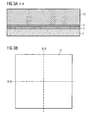
- Figure 3a illustrates a schematic cross-sectional view of a memory array region of a partially fabricated memory device in accordance with an embodiment of the present invention.
- Figure 3b illustrates a top view of the memory device shown in Figure 3a.
- Figure 3c illustrates a schematic cross-sectional view of a peripheral region of the memory device shown in Figure 3a.
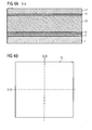
- Figure 4a illustrates a schematic cross-sectional view of a memory array region of a partially fabricated memory device in accordance with an embodiment of the present invention.
- Figure 4b illustrates a top view of the memory device shown in Figure 4a.
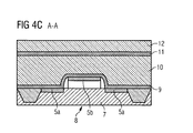
- Figure 4c illustrates a schematic cross-sectional view of a peripheral region of the memory device shown in Figure 4a.
- Figure 5a illustrates a schematic cross-sectional view of a memory array region of a partially fabricated memory device in accordance with an embodiment of the present invention.
- Figure 5b illustrates a top view of the memory device shown in Figure 5a.
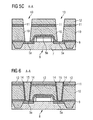
- Figure 5c illustrates a schematic cross-sectional view of a peripheral region of the memory device shown in Figure 5a.
- Figure 6 illustrates a schematic cross-sectional view of a peripheral region of a partially fabricated memory device in accordance with an embodiment of the present invention.
- Figure 7a illustrates a schematic cross-sectional view of a memory array region of a partially fabricated memory device in accordance with an embodiment of the present invention.
- Figure 7b illustrates a top view of the memory device shown in Figure 7a.
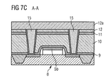
- Figure 7c illustrates a schematic cross-sectional view of a peripheral region of the memory device shown in Figure 7a.
- Figure 8a illustrates a schematic cross-sectional view of a memory array region of a partially fabricated memory device in accordance with an embodiment of the present invention.
- Figure 8b illustrates a top view of the memory device shown in Figure 8a.
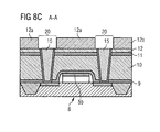
- Figure 8c illustrates a schematic cross-sectional view of a peripheral region of the memory device shown in Figure 8a.
- Figure 9a illustrates a schematic cross-sectional view of a memory array region of a partially fabricated memory device in accordance with an embodiment of the present invention.
- Figure 9b illustrates a top view of the memory device shown in Figure 9a.
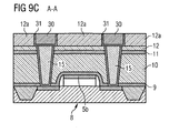
- Figure 9c illustrates a schematic cross-sectional view of a peripheral region of the memory device shown in Figure 9a.
- Figure 10a illustrates a schematic cross-sectional view of a memory array region of a partially fabricated memory device in accordance with an embodiment of the present invention.
- Figure 10b illustrates a top view of the memory device shown in Figure 10a.
- Figure 10c illustrates a schematic cross-sectional view of a peripheral region of the memory device shown in Figure 10a.
- Figure 10d illustrates a schematic cross-sectional view of the memory array region of the memory device shown in Figure 10a.
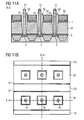
- Figure 11a illustrates a schematic cross-sectional view of a memory array region of a partially fabricated memory device in accordance with an embodiment of the present invention.
- Figure 11b illustrates a top view of the memory device shown in Figure 11a.
- Figure 12a illustrates a schematic cross-sectional view of a memory array region of a partially fabricated memory device in accordance with an embodiment of the present invention.
- Figure 12b illustrates a top view of the memory device shown in Figure 12a.
- Figure 12c illustrates a schematic cross-sectional view of the memory array region of the memory device shown in Figure 12a.
- Figure 1a illustrates a schematic cross-sectional view of a memory array region of a partially fabricated memory device 1 in accordance with an embodiment of the present invention.
- the memory device 1 preferably is a so-called “resistive” or “resistively switching” memory device, in particular, a Phase Change Random Access Memory (“PCRAM”) device.
- PCRAM Phase Change Random Access Memory
- the “resistively switching” memory device 1 as conventional “resistively switching” memory devices comprises an "active” or “switching active” material 2 which by appropriate switching processes is placed in a more or less conductive state (wherein e.g. the more conductive state corresponds to a stored logic "One”, and the less conductive state to a stored logic “Zero”, or vice versa).
- an appropriate chalcogenide or chalcogenide compound material may be used (here: e.g. a Ge-Sb-Te ("GST") compound material (or e.g. an Ag-In-Sb-Te compound material, etc.)).
- GST Ge-Sb-Te
- the chalcogenide compound material is adapted to be placed in an amorphous, i.e. a relatively weakly conductive, or a crystalline, i.e. a relatively strongly conductive state.
- the "switching active" material 2 other than in conventional Phase Change Random Access Memory (“PCRAM”) devices is not positioned between two respective electrodes, but between an electrode 3, and a nanowire transistor 4.
- an appropriate heating current pulse is applied to the switching active material 2, said heating current pulse resulting in that the switching active material 2 is heated beyond the crystallization temperature and crystallizes ("writing process").
- a change of state of the switching active material 2 from the crystalline, i.e. a relatively strongly conductive state, to the amorphous, i.e. a relatively weakly conductive state may, for instance, be achieved in that - again by means of an appropriate heating current pulse - the switching active material 2 is heated beyond the melting temperature and is subsequently “quenched” to an amorphous state by quick cooling ("erasing process").
- the above erase or write heating current pulses are provided via respective source lines 5, and via the above nanowire transistors 4 (in particular, respective n-p-n-doped regions 4a of the transistors 4) in direct contact with the switching active material 2.
- the respective erase or write heating current flows through the above electrodes 3 (also in direct contact with the switching active material 2), and respective bit lines (not shown) contacting the electrodes 3.
- n-p-n-doped regions 4a of the transistors 4 are surrounded by respective transistor gate regions 4b, additionally functioning as word lines.
- the nanowire transistors 4 are built in a vertical direction.
- the nanowire transistors 4 function as "access transistors", and - due to the direct contact between the n-p-n-doped regions 4a, and the switching active material 2 - additionally function as electrodes.
- the contact area between a respective n-p-n-doped region 4a, and a respective switching active material 2 is relatively small, leading to relatively high current density in the switching active material 2.
- Whether or not a respective transistor 4 is in a conductive state in which case a erase or write heating current pulse might flow from a respective source line 5 through a respective n-p-n-doped transistor region 4a to the associated switching active material 2) or a non-conductive state (preventing that a erase or write heating current pulse might flow from a respective source line 5 through a respective n-p-n-doped transistor region 4a to the associated switching active material 2) is determined by the state of the above word lines / transistor gate regions 4b.
- the above source lines 5 (and e.g. also the above bit lines contacting the electrodes 3) run through the memory device 1 in a direction A perpendicular to a direction B in which the word lines 4b run through the memory device 1.
- a respective switching active material 2 might be selected for writing / erasing by activating the respective word line 4b associated therewith, and applying a erase or write heating current pulse to the respective source line 5.
- TiN may be used, or e.g. W, Ti, Ta, or e.g. Cu, Ag, Au, Zn, etc., or e.g. WN, TaN, NbN, ZrN, HfN, or e.g. TiSiN, TaSiN, TiAlN, etc., or any other suitable material.
- Associated pairs of switching active material 2 / electrodes 3 are isolated from neighboring pairs of switching active material 2 / electrodes 3 by a suitable isolating material, e.g. SiO 2 (not shown).
- a suitable isolating material e.g. SiO 2 (not shown).
- the above STI-regions 6 are built in a respective silicon substrate 7.
- the STI-regions 6 both are built in a memory array region of the memory device 1 (shown in Figure 2a), as in a peripheral region of the memory device 1 (not shown).
- the STI-regions 6 extend in the above direction A, i.e., parallel to the source lines 5 (built after the STI-regions 6, see description below).
- respective transistors 8 for controlling e.g. the above word lines 4b, and/or the above source lines 5 (or more exactly: parts of the respective transistors 8) might be built.
- the above source lines 5 (and the above sources / drains 5a, and gates 5b) are formed.
- parts of the areas subject to the above salicidation process e.g., areas where no contacts shall be fabricated
- corresponding isolation layers might be deposited, e.g. first a SiN layer 9, and then a SiO 2 layer 10, covering e.g. the above source lines 5, and the STI-regions 6.
- ILD inter level dielectric
- a respective polishing might take place.
- the SiO 2 layer 10 e.g. has a height of between 200nm and 600nm, e.g. between 300nm and 500nm
- the SiN layer 9 e.g. has a height of between 5nm and 50nm, e.g. between 10nm and 30nm.
- a corresponding etch stop layer 11, and a further isolation layer 12 is deposited, e.g. first a SiC layer 11 as etch stop layer 11 (covering e.g. the above SiO 2 layer 10), and then a SiO 2 layer 12 as further isolation layer 12 (covering e.g. the above SiC layer 11).
- the SiC layer 11 e.g. has a height of between 5nm and 50nm, e.g. between 10nm and 30nm
- the SiO 2 layer 12 e.g. has a height of between 100nm and 400nm, e.g. between 150nm and 250nm.
- respective contact holes 13 are built, preferably by use of respective contact litho and etch processes, e.g. involving a 4-step etching, for instance a respective SiO 2 /SiC/SiO 2 /SiN-etching process.
- the contact holes 13 reach all through the above layers 9, 10, 11, 12, such that the above sources / drains 5a of the above peripheral transistors 8 are laid open.
- a liner 14, e.g. Ti/TiN is deposited, contacting - in a downward direction - the above sources / drains 5a of the above peripheral transistors 8, as well as - in a sideward direction - the above layers 9, 10, 11, 12.
- the contact holes 13 are filled with a respective filler material 15, e.g. tungsten.
- a respective polishing process is carried out, e.g. a respective CMP (chemical mechanical polishing) process.
- a further SiO 2 layer 12a is deposited.
- the SiO 2 layer 12 is increased in height to e.g. a SiO 2 layer 12b with a (total) height of e.g. between 200nm and 500nm, e.g. between 250nm and 350nm (see e.g. Figure 7a).
- the above SiO 2 layer 12b is etched, such that the above etch stop layer 11 (here e.g. the above SiC layer 11) is laid open.
- the regions 20 etched in the memory array region - just as the word lines / transistor gate regions 4b to be built later - extend in the above direction B all through the memory array region, i.e., perpendicular to the above direction A in which the source lines 5 run through the memory device 1. Further, adjacent regions 20 etched in the memory array region - just as adjacent word lines / transistor gate regions 4b to be built later - run parallel to each other.
- the regions 20 etched in the memory array region - just as the word lines / transistor gate regions 4b to be built later - may have a width of e.g. about 3F (whereby F represents the minimal structural size, for instance between 40nm and 80nm, e.g. between 50nm and 70nm, e.g. 65nm).
- F represents the minimal structural size, for instance between 40nm and 80nm, e.g. between 50nm and 70nm, e.g. 65nm).
- the distance between two adjacent regions 20 etched in the memory array region - just as the distance between two adjacent word lines / transistor gate regions 4b to be built later - may e.g. be about 1F.
- regions 21 directly above the source lines 5 - more particular, regions 21 where the above transistors 4 (more specifically the n-p-n-doped transistor regions 4a, see Figure 1a) are to built later - are left standing.
- the regions 21 may e.g. have a substantially rectangular or square cross-section, and e.g. may have a width and length of e.g. about 1F. Further, the distance between adjacent regions 21 may e.g. also be about 1F.
- a TaN/Ta barrier 31 is deposited in the etched regions 20 (e.g., in the peripheral region of the memory device 1, on the surface of the filler material 15, and on side walls of the layer 12a (see Figure 9c), and in the memory array region, on the surface of the layer 11, and on side walls of the layer 12b / the above regions 21 (see Figure 9a)).
- a respective metal 30, e.g., Cu is deposited electrochemically, for instance, by carrying out a respective Cu plating process.
- a respective polishing process is carried out, e.g. a CMP (chemical mechanical polishing) process.
- a respective litho and etch process is carried out.
- a respective litho and etch process is carried out.
- both the peripheral region of the memory device 1 (see Figure 10c) and the memory array region of the memory device 1 (see Figures 10a, 10b) are covered with a respective resist 40.
- the resist 40 - in parts of the memory array region (see below), but not in the peripheral region - is irradiated (e.g. exposed to light), and developed, such that the resist 40 in irradiated (exposed) regions 41 may be removed.
- the remaining - non-removed - resist 40 in the memory array region has the form of stripes extending in the above direction B all through the memory array region (parallel to the word lines / transistor gate regions 4b, and perpendicular to the above direction A in which the source lines 5 run through the memory device 1).
- the stripes of the remaining resist 40 in the memory array region e.g. may have a width of e.g. about 2F.
- the longitudinal middle axis of the above irradiated regions 41 where the resist 40 is removed is centered on the longitudinal middle axis of the above regions 21, shown in Figure 8a, 8b, which were left standing when carrying out the above metal 1 litho and etch processes described in connection with Figures 8a, 8b (i.e., is centered with regard to the longitudinal middle axis of the regions 21 where the above n-p-n-doped transistor regions 4a, see Figure 1a are to built later).
- respective contact holes 50 are built, preferably - correspondingly similar to the processes used for building the above contact holes 13 in the peripheral region, and as described with respect to Figure 5c - by use of a respective 4-step etching, for instance a respective SiO 2 /SiC/SiO 2 /SiN-etching process.
- the contact holes 50 reach all through the above layers 9, 10, 11, 12b (more particularly: the above regions 21 left standing) - however, not through the above metal 30, as the above copper metal and TaN/Ta barrier 31 prevents etching thereof - such that the above source lines 5 partly are laid open.
- an etching is performed which is self-aligned with respect to the above 1 st metal layer, here: the transistor gate regions / word lines 4b.
- the (remaining) resist 40 is removed in both the memory array region and the peripheral region of the memory device 1.
- n-p-n-doped transistor regions 4a are built in the above contact holes 50.
- a catalyst 51 is deposited on the surface of the laid open, exposed parts of the source lines 5, e.g. by use of a respective electroless deposition process.
- the catalyst 51 e.g. primarily might comprise a respective silicide forming metal such as e.g. Ti, Pd, Pt, Au, Cu, Co, Cr, Hf, Ir, Mn, Mo, Ni, Rh, Ta, W, Zr, etc.
- the catalyst 51 deposited on the surface of the (laid open, exposed) parts of the source lines 5 might be heated, such that its area is reduced by coagulation.
- the contact area between the yet-to-be-built n-p-n-doped transistor regions 4a, and the switching active material 2 (also to be built later) might be further reduced, additionally enhancing the current density in the switching active material 2.
- a respective nanowire / nanotube / nanofibre is grown in the contact holes 50 (e.g. a respective Si nanowire, as e.g. described in Cui, Y.; Duan, X.; Hu, J.; Lieber, C.M.: J. Phys. Chem. B 2000, 103, 5213 , or any other suitable nanowire / nanotube / nanofibre, e.g. a respective carbon nanowire / nanotube / nanofibre, etc.), so as to finally form the above n-p-n-doped transistor regions 4a.
- a respective Si nanowire as e.g. described in Cui, Y.; Duan, X.; Hu, J.; Lieber, C.M.: J. Phys. Chem. B 2000, 103, 5213 , or any other suitable nanowire / nanotube / nanofibre, e.g. a respective carbon nanowire / nanotube / nanofibre, etc
- the catalyst 51 (not shown in Figure 11b) whilst the respective nanowire / nanotube / nanofibre is growing keeps staying on top of it.
- an empty space is left between the nanowire / nanotube / nanofibre, and the above layers 9, 10, 11 / the above barrier 31.
- the nanowire / nanotube / nanofibre may have a cross-section which is substantially circular.
- the diameter of the nanowire / nanotube / nanofibre may be relatively small, e.g. below 1F, for instance between 0.1F and 1F, e.g. between 0.2F and 0.5F, etc.
- a bottom section of the nanowire / nanotube / nanofibre may be n-doped (or alternatively: p-doped), a middle section of the nanowire / nanotube / nanofibre may be p-doped (or alternatively: n-doped), and an upper section of the nanowire / nanotube / nanofibre may again be n-doped (or alternatively: p-doped).
- the respective doping of the nanowire / nanotube / nanofibre may be achieved by e.g. adding respective gases into the atmosphere during the growth of the nanowire / nanotube / nanofibre.
- PH 3 may be added to the atmosphere so as to achieve a respective n-doping of the bottom section of the nanowire / nanotube / nanofibre.
- middle section of the nanowire / nanotube / nanofibre e.g. B 2 H 6 may be added to the atmosphere so as to achieve a respective p-doping of the middle section of the nanowire / nanotube / nanofibre.
- upper section of the nanowire / nanotube / nanofibre e.g. again PH 3 may be added to the atmosphere so as to achieve a respective n-doping of the upper section of the nanowire / nanotube / nanofibre.
- the gate-oxide of the transistors 4 is formed, e.g. by conformly depositing SiO 2 i) in the above empty space between the nanowire / nanotube / nanofibre, and the layers 9, 10, 11 / the barrier 31, and ii) above the metal 30 (here: Cu) / above the barrier 31 (see e.g. the SiO 2 layer 60 shown in Figures 12a, 12b, 12c).
- a respective thermal SiO 2 deposition process might be used, and / or (in particular for the above step ii)) e.g.
- a respective CVD (chemical vapor deposition) or ALD (atomic layer deposition) process etc.
- a respective polishing process is carried out, e.g. a respective CMP (chemical mechanical polishing) process, whereby the above catalyst 51 on top of the nanowire / nanotube / nanofibre is removed.
- the "switching active” material 2 for instance, the above Ge-Sb-Te (“GST”) compound material 2 is deposited (here: on the upper surface of the nanowire / nanotube / nanofibre, and the upper surface of the above SiO 2 layer 60, i.e., the whole memory array region).
- the "switching active” material 2 e.g. a respective PVD (physical vapor deposition) process, or e.g. a respective CVD (chemical vapor deposition) process might be used.
- the electrode 3 is deposited on the "switching active" material 2, i.e., the whole memory array region. Thereafter, corresponding litho and etch processes are carried out such as to achieve that the electrode 3 and the "switching active" material 2 - as shown in Figure 1b - both e.g. have a substantially rectangular or square cross-section, and e.g. may have a width and length of e.g. about 1F.
- PCRAM Phase Change Random Access Memory
- the vertical axis of the "switching active" material 2 (and the electrode 3) is centered on the vertical axis of the nanowire / nanotube / nanofibre (i.e., the n-p-n-doped transistor regions 4a).
- the lower surface of the "switching active” material 2 contacts the upper surface of the nanowire / nanotube / nanofibre (and the upper surface of those parts of the SiO 2 layer 60 which surround the nanowire / nanotube / nanofibre).
- the above isolating material e.g. SiO 2 is deposited, which isolates associated pairs of switching active material 2 / electrodes 3 from neighboring pairs of switching active material 2 / electrodes 3.
- a respective polishing process is carried out, e.g. a respective CMP (chemical mechanical polishing) process (such as to polish the upper surface of the isolating material, and the electrode 3).
- CMP chemical mechanical polishing
Landscapes
- Chemical & Material Sciences (AREA)
- Crystallography & Structural Chemistry (AREA)
- Semiconductor Memories (AREA)
Applications Claiming Priority (1)
| Application Number | Priority Date | Filing Date | Title |
|---|---|---|---|
| US11/445,801 US7626190B2 (en) | 2006-06-02 | 2006-06-02 | Memory device, in particular phase change random access memory device with transistor, and method for fabricating a memory device |
Publications (1)
| Publication Number | Publication Date |
|---|---|
| EP1863092A2 true EP1863092A2 (de) | 2007-12-05 |
Family
ID=38420577
Family Applications (1)
| Application Number | Title | Priority Date | Filing Date |
|---|---|---|---|
| EP07008964A Withdrawn EP1863092A2 (de) | 2006-06-02 | 2007-05-03 | Speichervorrichtung, insbesondere Phasenwechselspeicher mit wahlfreiem Zugriff, mit Nanodraht-Transistor und Verfahren zur Herstellung der Speichervorrichtung |
Country Status (5)
| Country | Link |
|---|---|
| US (1) | US7626190B2 (de) |
| EP (1) | EP1863092A2 (de) |
| JP (1) | JP2007324600A (de) |
| KR (1) | KR20070115707A (de) |
| CN (1) | CN101093850A (de) |
Families Citing this family (23)
| Publication number | Priority date | Publication date | Assignee | Title |
|---|---|---|---|---|
| US7776758B2 (en) | 2004-06-08 | 2010-08-17 | Nanosys, Inc. | Methods and devices for forming nanostructure monolayers and devices including such monolayers |
| US7968273B2 (en) * | 2004-06-08 | 2011-06-28 | Nanosys, Inc. | Methods and devices for forming nanostructure monolayers and devices including such monolayers |
| KR100674144B1 (ko) * | 2006-01-05 | 2007-01-29 | 한국과학기술원 | 탄소 나노 튜브를 이용한 상변화 메모리 및 이의 제조 방법 |
| US20070292985A1 (en) * | 2006-06-16 | 2007-12-20 | Yuegang Zhang | Phase change memory with nanofiber heater |
| US8030637B2 (en) * | 2006-08-25 | 2011-10-04 | Qimonda Ag | Memory element using reversible switching between SP2 and SP3 hybridized carbon |
| US7510960B2 (en) * | 2006-08-29 | 2009-03-31 | International Business Machines Corporation | Bridge for semiconductor internal node |
| US20080078983A1 (en) * | 2006-09-28 | 2008-04-03 | Wolfgang Raberg | Layer structures comprising chalcogenide materials |
| US20080102278A1 (en) * | 2006-10-27 | 2008-05-01 | Franz Kreupl | Carbon filament memory and method for fabrication |
| US7915603B2 (en) * | 2006-10-27 | 2011-03-29 | Qimonda Ag | Modifiable gate stack memory element |
| US20080246076A1 (en) * | 2007-01-03 | 2008-10-09 | Nanosys, Inc. | Methods for nanopatterning and production of nanostructures |
| US20090136785A1 (en) * | 2007-01-03 | 2009-05-28 | Nanosys, Inc. | Methods for nanopatterning and production of magnetic nanostructures |
| US7719039B2 (en) * | 2007-09-28 | 2010-05-18 | Freescale Semiconductor, Inc. | Phase change memory structures including pillars |
| US7811851B2 (en) * | 2007-09-28 | 2010-10-12 | Freescale Semiconductor, Inc. | Phase change memory structures |
| KR100920049B1 (ko) | 2007-12-21 | 2009-10-07 | 주식회사 하이닉스반도체 | 박막 패턴 형성방법 및 이를 이용한 반도체 소자의제조방법 |
| US8206804B2 (en) * | 2008-08-29 | 2012-06-26 | Corning Incorporated | Phase change memory materials |
| US8384007B2 (en) * | 2009-10-07 | 2013-02-26 | Zena Technologies, Inc. | Nano wire based passive pixel image sensor |
| KR20100052080A (ko) * | 2008-11-10 | 2010-05-19 | 주식회사 하이닉스반도체 | 저항성 메모리 소자 및 그 제조 방법 |
| KR20110032252A (ko) * | 2009-09-22 | 2011-03-30 | 삼성전자주식회사 | 수직 어레이 트랜지스터를 갖는 저항성 메모리 소자 |
| JP4913190B2 (ja) | 2009-09-24 | 2012-04-11 | 株式会社東芝 | 不揮発性記憶装置 |
| US20110169136A1 (en) * | 2010-01-14 | 2011-07-14 | Pickett Matthew D | Crossbar-integrated memristor array and method employing interstitial low dielectric constant insulator |
| KR102510707B1 (ko) * | 2016-07-12 | 2023-03-17 | 에스케이하이닉스 주식회사 | 전자 장치 및 그 제조 방법 |
| US20190181337A1 (en) * | 2016-09-25 | 2019-06-13 | Intel Corporation | Barriers for metal filament memory devices |
| KR102295524B1 (ko) * | 2017-03-27 | 2021-08-30 | 삼성전자 주식회사 | 메모리 소자 |
Family Cites Families (18)
| Publication number | Priority date | Publication date | Assignee | Title |
|---|---|---|---|---|
| CA2442985C (en) * | 2001-03-30 | 2016-05-31 | The Regents Of The University Of California | Methods of fabricating nanostructures and nanowires and devices fabricated therefrom |
| JP3948292B2 (ja) * | 2002-02-01 | 2007-07-25 | 株式会社日立製作所 | 半導体記憶装置及びその製造方法 |
| US7151273B2 (en) * | 2002-02-20 | 2006-12-19 | Micron Technology, Inc. | Silver-selenide/chalcogenide glass stack for resistance variable memory |
| US6515325B1 (en) * | 2002-03-06 | 2003-02-04 | Micron Technology, Inc. | Nanotube semiconductor devices and methods for making the same |
| US6891227B2 (en) | 2002-03-20 | 2005-05-10 | International Business Machines Corporation | Self-aligned nanotube field effect transistor and method of fabricating same |
| KR100504701B1 (ko) * | 2003-06-11 | 2005-08-02 | 삼성전자주식회사 | 상변화 기억 소자 및 그 형성 방법 |
| DE10331528A1 (de) | 2003-07-11 | 2005-02-03 | Infineon Technologies Ag | DRAM-Halbleiterspeicherzelle sowie Verfahren zu deren Herstellung |
| DE10335813B4 (de) * | 2003-08-05 | 2009-02-12 | Infineon Technologies Ag | IC-Chip mit Nanowires |
| EP1508926A1 (de) * | 2003-08-19 | 2005-02-23 | Hitachi, Ltd. | Nanoröhren-Transistor |
| US7829883B2 (en) * | 2004-02-12 | 2010-11-09 | International Business Machines Corporation | Vertical carbon nanotube field effect transistors and arrays |
| DE102004007633B4 (de) * | 2004-02-17 | 2010-10-14 | Qimonda Ag | Speicherzelle, Halbleiter-Speicherbauelement und Verfahren zur Herstellung einer Speicherzelle |
| JP2005347378A (ja) * | 2004-06-01 | 2005-12-15 | Canon Inc | ナノカーボン材料のパターン形成方法、並びに、半導体デバイス及びその製造方法 |
| WO2006003620A1 (en) | 2004-06-30 | 2006-01-12 | Koninklijke Philips Electronics N.V. | Method for manufacturing an electric device with a layer of conductive material contacted by nanowire |
| US20060034116A1 (en) * | 2004-08-13 | 2006-02-16 | Lam Chung H | Cross point array cell with series connected semiconductor diode and phase change storage media |
| WO2006035325A1 (en) | 2004-09-27 | 2006-04-06 | Koninklijke Philips Electronics N.V. | Electric device with nanowires comprising a phase change material |
| KR100590568B1 (ko) * | 2004-11-09 | 2006-06-19 | 삼성전자주식회사 | 멀티 비트 플래시 메모리 소자 및 동작 방법 |
| JP4410095B2 (ja) * | 2004-12-27 | 2010-02-03 | 株式会社東芝 | 半導体メモリ |
| US20070183189A1 (en) * | 2006-02-08 | 2007-08-09 | Thomas Nirschl | Memory having nanotube transistor access device |
-
2006
- 2006-06-02 US US11/445,801 patent/US7626190B2/en not_active Expired - Fee Related
-
2007
- 2007-05-03 EP EP07008964A patent/EP1863092A2/de not_active Withdrawn
- 2007-05-30 KR KR1020070052588A patent/KR20070115707A/ko not_active Ceased
- 2007-06-01 JP JP2007147006A patent/JP2007324600A/ja active Pending
- 2007-06-01 CN CN200710106474.4A patent/CN101093850A/zh active Pending
Also Published As
| Publication number | Publication date |
|---|---|
| US7626190B2 (en) | 2009-12-01 |
| US20070278530A1 (en) | 2007-12-06 |
| CN101093850A (zh) | 2007-12-26 |
| KR20070115707A (ko) | 2007-12-06 |
| JP2007324600A (ja) | 2007-12-13 |
Similar Documents
| Publication | Publication Date | Title |
|---|---|---|
| EP1863092A2 (de) | Speichervorrichtung, insbesondere Phasenwechselspeicher mit wahlfreiem Zugriff, mit Nanodraht-Transistor und Verfahren zur Herstellung der Speichervorrichtung | |
| CN109860387B (zh) | 具有选择器件的pcram结构 | |
| US9659998B1 (en) | Memory having an interlayer insulating structure with different thermal resistance | |
| US7362608B2 (en) | Phase change memory fabricated using self-aligned processing | |
| US7545668B2 (en) | Mushroom phase change memory having a multilayer electrode | |
| CN111129066B (zh) | 相变化随机存取记忆体装置及其制造方法 | |
| US8426840B2 (en) | Nonvolatile memory cells having phase changeable patterns therein for data storage | |
| US7875492B2 (en) | Integrated circuit including a memory fabricated using self-aligned processing | |
| CN102522374B (zh) | 一种具有柱状底电极相变化存储装置及其制造方法 | |
| US7728319B2 (en) | Vertical phase change memory cell and methods for manufacturing thereof | |
| US7442602B2 (en) | Methods of fabricating phase change memory cells having a cell diode and a bottom electrode self-aligned with each other | |
| US8426967B2 (en) | Scaled-down phase change memory cell in recessed heater | |
| EP1830409A2 (de) | Mittels selbstausrichtender Verarbeitung hergestellter Phasenwechselspeicher | |
| US7869257B2 (en) | Integrated circuit including diode memory cells | |
| TW201803168A (zh) | 具有高耐久性之相變化記憶體的積體電路及其製造方法 | |
| US8853044B2 (en) | Phase-change random access memory device and method of manufacturing the same | |
| US7545019B2 (en) | Integrated circuit including logic portion and memory portion | |
| US7671354B2 (en) | Integrated circuit including spacer defined electrode | |
| CN101286522A (zh) | 相变存储装置及其制造方法和操作方法 | |
| US7745812B2 (en) | Integrated circuit including vertical diode | |
| US20080135825A1 (en) | Phase-change memory device and method of fabricating the same | |
| US20130193402A1 (en) | Phase-change random access memory device and method of manufacturing the same | |
| KR100650752B1 (ko) | 상변환 기억 소자 및 그의 제조방법 | |
| US20080315171A1 (en) | Integrated circuit including vertical diode |
Legal Events
| Date | Code | Title | Description |
|---|---|---|---|
| PUAI | Public reference made under article 153(3) epc to a published international application that has entered the european phase |
Free format text: ORIGINAL CODE: 0009012 |
|
| AK | Designated contracting states |
Kind code of ref document: A2 Designated state(s): AT BE BG CH CY CZ DE DK EE ES FI FR GB GR HU IE IS IT LI LT LU LV MC MT NL PL PT RO SE SI SK TR |
|
| AX | Request for extension of the european patent |
Extension state: AL BA HR MK YU |
|
| 19U | Interruption of proceedings before grant |
Effective date: 20090401 |
|
| 19W | Proceedings resumed before grant after interruption of proceedings |
Effective date: 20091123 |
|
| STAA | Information on the status of an ep patent application or granted ep patent |
Free format text: STATUS: THE APPLICATION IS DEEMED TO BE WITHDRAWN |
|
| 18D | Application deemed to be withdrawn |
Effective date: 20091201 |