EP1860173B1 - White light-emitting lamp, backlight using same, display and illuminating device - Google Patents
White light-emitting lamp, backlight using same, display and illuminating device Download PDFInfo
- Publication number
- EP1860173B1 EP1860173B1 EP06714557.3A EP06714557A EP1860173B1 EP 1860173 B1 EP1860173 B1 EP 1860173B1 EP 06714557 A EP06714557 A EP 06714557A EP 1860173 B1 EP1860173 B1 EP 1860173B1
- Authority
- EP
- European Patent Office
- Prior art keywords
- phosphor
- light
- emitting
- white light
- activated
- Prior art date
- Legal status (The legal status is an assumption and is not a legal conclusion. Google has not performed a legal analysis and makes no representation as to the accuracy of the status listed.)
- Active
Links
- OAICVXFJPJFONN-UHFFFAOYSA-N Phosphorus Chemical compound [P] OAICVXFJPJFONN-UHFFFAOYSA-N 0.000 claims description 177
- 229910052693 Europium Inorganic materials 0.000 claims description 54
- 229910052772 Samarium Inorganic materials 0.000 claims description 28
- 229910052984 zinc sulfide Inorganic materials 0.000 claims description 28
- 229920005989 resin Polymers 0.000 claims description 27
- 239000011347 resin Substances 0.000 claims description 27
- 239000011572 manganese Substances 0.000 claims description 26
- 239000010949 copper Substances 0.000 claims description 24
- 239000000203 mixture Substances 0.000 claims description 23
- 239000010931 gold Substances 0.000 claims description 22
- 229910052748 manganese Inorganic materials 0.000 claims description 21
- 229910052782 aluminium Inorganic materials 0.000 claims description 20
- 229910052802 copper Inorganic materials 0.000 claims description 20
- 239000004973 liquid crystal related substance Substances 0.000 claims description 20
- 229910052737 gold Inorganic materials 0.000 claims description 16
- -1 aluminum-activated zinc sulfide phosphor Chemical class 0.000 claims description 15
- OGPBJKLSAFTDLK-UHFFFAOYSA-N europium atom Chemical compound [Eu] OGPBJKLSAFTDLK-UHFFFAOYSA-N 0.000 claims description 15
- 239000002245 particle Substances 0.000 claims description 13
- 150000004645 aluminates Chemical class 0.000 claims description 12
- 239000004065 semiconductor Substances 0.000 claims description 12
- 230000010354 integration Effects 0.000 claims description 11
- 229910052788 barium Inorganic materials 0.000 claims description 9
- 239000011230 binding agent Substances 0.000 claims description 9
- 239000011163 secondary particle Substances 0.000 claims description 7
- RYGMFSIKBFXOCR-UHFFFAOYSA-N Copper Chemical compound [Cu] RYGMFSIKBFXOCR-UHFFFAOYSA-N 0.000 claims description 6
- 229910052749 magnesium Inorganic materials 0.000 claims description 6
- PCHJSUWPFVWCPO-UHFFFAOYSA-N gold Chemical compound [Au] PCHJSUWPFVWCPO-UHFFFAOYSA-N 0.000 claims description 5
- 239000011164 primary particle Substances 0.000 claims description 5
- 239000011701 zinc Substances 0.000 claims description 2
- 229910052725 zinc Inorganic materials 0.000 claims description 2
- NYZGMENMNUBUFC-UHFFFAOYSA-N P.[S-2].[Zn+2] Chemical class P.[S-2].[Zn+2] NYZGMENMNUBUFC-UHFFFAOYSA-N 0.000 description 22
- 238000009877 rendering Methods 0.000 description 15
- 238000000295 emission spectrum Methods 0.000 description 13
- YELHQTOAIOZZMW-UHFFFAOYSA-N [P].O=S.[La] Chemical class [P].O=S.[La] YELHQTOAIOZZMW-UHFFFAOYSA-N 0.000 description 12
- 230000000052 comparative effect Effects 0.000 description 9
- 238000010586 diagram Methods 0.000 description 6
- 238000011156 evaluation Methods 0.000 description 6
- 230000000694 effects Effects 0.000 description 5
- 229910052746 lanthanum Inorganic materials 0.000 description 5
- 229920002050 silicone resin Polymers 0.000 description 5
- 239000003513 alkali Substances 0.000 description 4
- ITVPBBDAZKBMRP-UHFFFAOYSA-N chloro-dioxido-oxo-$l^{5}-phosphane;hydron Chemical compound OP(O)(Cl)=O ITVPBBDAZKBMRP-UHFFFAOYSA-N 0.000 description 4
- 238000004891 communication Methods 0.000 description 4
- 238000012545 processing Methods 0.000 description 4
- UPIZSELIQBYSMU-UHFFFAOYSA-N lanthanum;sulfur monoxide Chemical class [La].S=O UPIZSELIQBYSMU-UHFFFAOYSA-N 0.000 description 3
- 230000002093 peripheral effect Effects 0.000 description 3
- DRDVZXDWVBGGMH-UHFFFAOYSA-N zinc;sulfide Chemical compound [S-2].[Zn+2] DRDVZXDWVBGGMH-UHFFFAOYSA-N 0.000 description 3
- 239000004925 Acrylic resin Substances 0.000 description 2
- 229920000178 Acrylic resin Polymers 0.000 description 2
- 239000003086 colorant Substances 0.000 description 2
- 229910052909 inorganic silicate Inorganic materials 0.000 description 2
- 239000011159 matrix material Substances 0.000 description 2
- 230000003287 optical effect Effects 0.000 description 2
- 239000002002 slurry Substances 0.000 description 2
- 239000000758 substrate Substances 0.000 description 2
- BTBUEUYNUDRHOZ-UHFFFAOYSA-N Borate Chemical compound [O-]B([O-])[O-] BTBUEUYNUDRHOZ-UHFFFAOYSA-N 0.000 description 1
- PWHULOQIROXLJO-UHFFFAOYSA-N Manganese Chemical compound [Mn] PWHULOQIROXLJO-UHFFFAOYSA-N 0.000 description 1
- 239000004677 Nylon Substances 0.000 description 1
- FFJZODLGGHJTTI-UHFFFAOYSA-N O=S.[Y].[P] Chemical class O=S.[Y].[P] FFJZODLGGHJTTI-UHFFFAOYSA-N 0.000 description 1
- BPQQTUXANYXVAA-UHFFFAOYSA-N Orthosilicate Chemical compound [O-][Si]([O-])([O-])[O-] BPQQTUXANYXVAA-UHFFFAOYSA-N 0.000 description 1
- 239000005083 Zinc sulfide Substances 0.000 description 1
- 238000010521 absorption reaction Methods 0.000 description 1
- XAGFODPZIPBFFR-UHFFFAOYSA-N aluminium Chemical compound [Al] XAGFODPZIPBFFR-UHFFFAOYSA-N 0.000 description 1
- 150000001875 compounds Chemical class 0.000 description 1
- 230000006866 deterioration Effects 0.000 description 1
- 238000009792 diffusion process Methods 0.000 description 1
- 239000006185 dispersion Substances 0.000 description 1
- 239000000839 emulsion Substances 0.000 description 1
- 239000003822 epoxy resin Substances 0.000 description 1
- 150000002603 lanthanum Chemical class 0.000 description 1
- 230000031700 light absorption Effects 0.000 description 1
- 238000000034 method Methods 0.000 description 1
- 150000004767 nitrides Chemical class 0.000 description 1
- 229920001778 nylon Polymers 0.000 description 1
- 229920000647 polyepoxide Polymers 0.000 description 1
- 238000012552 review Methods 0.000 description 1
- KZUNJOHGWZRPMI-UHFFFAOYSA-N samarium atom Chemical compound [Sm] KZUNJOHGWZRPMI-UHFFFAOYSA-N 0.000 description 1
- 238000007789 sealing Methods 0.000 description 1
- 230000035945 sensitivity Effects 0.000 description 1
- 239000007787 solid Substances 0.000 description 1
- 238000001228 spectrum Methods 0.000 description 1
- XTQHKBHJIVJGKJ-UHFFFAOYSA-N sulfur monoxide Chemical compound S=O XTQHKBHJIVJGKJ-UHFFFAOYSA-N 0.000 description 1
Images
Classifications
-
- G—PHYSICS
- G02—OPTICS
- G02F—OPTICAL DEVICES OR ARRANGEMENTS FOR THE CONTROL OF LIGHT BY MODIFICATION OF THE OPTICAL PROPERTIES OF THE MEDIA OF THE ELEMENTS INVOLVED THEREIN; NON-LINEAR OPTICS; FREQUENCY-CHANGING OF LIGHT; OPTICAL LOGIC ELEMENTS; OPTICAL ANALOGUE/DIGITAL CONVERTERS
- G02F1/00—Devices or arrangements for the control of the intensity, colour, phase, polarisation or direction of light arriving from an independent light source, e.g. switching, gating or modulating; Non-linear optics
- G02F1/01—Devices or arrangements for the control of the intensity, colour, phase, polarisation or direction of light arriving from an independent light source, e.g. switching, gating or modulating; Non-linear optics for the control of the intensity, phase, polarisation or colour
- G02F1/13—Devices or arrangements for the control of the intensity, colour, phase, polarisation or direction of light arriving from an independent light source, e.g. switching, gating or modulating; Non-linear optics for the control of the intensity, phase, polarisation or colour based on liquid crystals, e.g. single liquid crystal display cells
- G02F1/133—Constructional arrangements; Operation of liquid crystal cells; Circuit arrangements
- G02F1/1333—Constructional arrangements; Manufacturing methods
- G02F1/1335—Structural association of cells with optical devices, e.g. polarisers or reflectors
- G02F1/1336—Illuminating devices
- G02F1/133602—Direct backlight
- G02F1/133603—Direct backlight with LEDs
-
- C—CHEMISTRY; METALLURGY
- C09—DYES; PAINTS; POLISHES; NATURAL RESINS; ADHESIVES; COMPOSITIONS NOT OTHERWISE PROVIDED FOR; APPLICATIONS OF MATERIALS NOT OTHERWISE PROVIDED FOR
- C09K—MATERIALS FOR MISCELLANEOUS APPLICATIONS, NOT PROVIDED FOR ELSEWHERE
- C09K11/00—Luminescent, e.g. electroluminescent, chemiluminescent materials
- C09K11/08—Luminescent, e.g. electroluminescent, chemiluminescent materials containing inorganic luminescent materials
- C09K11/58—Luminescent, e.g. electroluminescent, chemiluminescent materials containing inorganic luminescent materials containing copper, silver or gold
- C09K11/582—Chalcogenides
- C09K11/584—Chalcogenides with zinc or cadmium
-
- C—CHEMISTRY; METALLURGY
- C09—DYES; PAINTS; POLISHES; NATURAL RESINS; ADHESIVES; COMPOSITIONS NOT OTHERWISE PROVIDED FOR; APPLICATIONS OF MATERIALS NOT OTHERWISE PROVIDED FOR
- C09K—MATERIALS FOR MISCELLANEOUS APPLICATIONS, NOT PROVIDED FOR ELSEWHERE
- C09K11/00—Luminescent, e.g. electroluminescent, chemiluminescent materials
- C09K11/08—Luminescent, e.g. electroluminescent, chemiluminescent materials containing inorganic luminescent materials
- C09K11/64—Luminescent, e.g. electroluminescent, chemiluminescent materials containing inorganic luminescent materials containing aluminium
- C09K11/641—Chalcogenides
- C09K11/642—Chalcogenides with zinc or cadmium
-
- C—CHEMISTRY; METALLURGY
- C09—DYES; PAINTS; POLISHES; NATURAL RESINS; ADHESIVES; COMPOSITIONS NOT OTHERWISE PROVIDED FOR; APPLICATIONS OF MATERIALS NOT OTHERWISE PROVIDED FOR
- C09K—MATERIALS FOR MISCELLANEOUS APPLICATIONS, NOT PROVIDED FOR ELSEWHERE
- C09K11/00—Luminescent, e.g. electroluminescent, chemiluminescent materials
- C09K11/08—Luminescent, e.g. electroluminescent, chemiluminescent materials containing inorganic luminescent materials
- C09K11/77—Luminescent, e.g. electroluminescent, chemiluminescent materials containing inorganic luminescent materials containing rare earth metals
- C09K11/7728—Luminescent, e.g. electroluminescent, chemiluminescent materials containing inorganic luminescent materials containing rare earth metals containing europium
- C09K11/7734—Aluminates
-
- C—CHEMISTRY; METALLURGY
- C09—DYES; PAINTS; POLISHES; NATURAL RESINS; ADHESIVES; COMPOSITIONS NOT OTHERWISE PROVIDED FOR; APPLICATIONS OF MATERIALS NOT OTHERWISE PROVIDED FOR
- C09K—MATERIALS FOR MISCELLANEOUS APPLICATIONS, NOT PROVIDED FOR ELSEWHERE
- C09K11/00—Luminescent, e.g. electroluminescent, chemiluminescent materials
- C09K11/08—Luminescent, e.g. electroluminescent, chemiluminescent materials containing inorganic luminescent materials
- C09K11/77—Luminescent, e.g. electroluminescent, chemiluminescent materials containing inorganic luminescent materials containing rare earth metals
- C09K11/7728—Luminescent, e.g. electroluminescent, chemiluminescent materials containing inorganic luminescent materials containing rare earth metals containing europium
- C09K11/7737—Phosphates
- C09K11/7738—Phosphates with alkaline earth metals
- C09K11/7739—Phosphates with alkaline earth metals with halogens
-
- C—CHEMISTRY; METALLURGY
- C09—DYES; PAINTS; POLISHES; NATURAL RESINS; ADHESIVES; COMPOSITIONS NOT OTHERWISE PROVIDED FOR; APPLICATIONS OF MATERIALS NOT OTHERWISE PROVIDED FOR
- C09K—MATERIALS FOR MISCELLANEOUS APPLICATIONS, NOT PROVIDED FOR ELSEWHERE
- C09K11/00—Luminescent, e.g. electroluminescent, chemiluminescent materials
- C09K11/08—Luminescent, e.g. electroluminescent, chemiluminescent materials containing inorganic luminescent materials
- C09K11/77—Luminescent, e.g. electroluminescent, chemiluminescent materials containing inorganic luminescent materials containing rare earth metals
- C09K11/7783—Luminescent, e.g. electroluminescent, chemiluminescent materials containing inorganic luminescent materials containing rare earth metals containing two or more rare earth metals one of which being europium
- C09K11/7784—Chalcogenides
- C09K11/7787—Oxides
- C09K11/7789—Oxysulfides
-
- G—PHYSICS
- G02—OPTICS
- G02B—OPTICAL ELEMENTS, SYSTEMS OR APPARATUS
- G02B6/00—Light guides; Structural details of arrangements comprising light guides and other optical elements, e.g. couplings
- G02B6/0001—Light guides; Structural details of arrangements comprising light guides and other optical elements, e.g. couplings specially adapted for lighting devices or systems
- G02B6/0003—Light guides; Structural details of arrangements comprising light guides and other optical elements, e.g. couplings specially adapted for lighting devices or systems the light guides being doped with fluorescent agents
-
- G—PHYSICS
- G02—OPTICS
- G02B—OPTICAL ELEMENTS, SYSTEMS OR APPARATUS
- G02B6/00—Light guides; Structural details of arrangements comprising light guides and other optical elements, e.g. couplings
- G02B6/0001—Light guides; Structural details of arrangements comprising light guides and other optical elements, e.g. couplings specially adapted for lighting devices or systems
- G02B6/0011—Light guides; Structural details of arrangements comprising light guides and other optical elements, e.g. couplings specially adapted for lighting devices or systems the light guides being planar or of plate-like form
- G02B6/0033—Means for improving the coupling-out of light from the light guide
- G02B6/0035—Means for improving the coupling-out of light from the light guide provided on the surface of the light guide or in the bulk of it
- G02B6/0045—Means for improving the coupling-out of light from the light guide provided on the surface of the light guide or in the bulk of it by shaping at least a portion of the light guide
- G02B6/0046—Tapered light guide, e.g. wedge-shaped light guide
-
- H—ELECTRICITY
- H01—ELECTRIC ELEMENTS
- H01L—SEMICONDUCTOR DEVICES NOT COVERED BY CLASS H10
- H01L33/00—Semiconductor devices having potential barriers specially adapted for light emission; Processes or apparatus specially adapted for the manufacture or treatment thereof or of parts thereof; Details thereof
- H01L33/48—Semiconductor devices having potential barriers specially adapted for light emission; Processes or apparatus specially adapted for the manufacture or treatment thereof or of parts thereof; Details thereof characterised by the semiconductor body packages
- H01L33/50—Wavelength conversion elements
- H01L33/501—Wavelength conversion elements characterised by the materials, e.g. binder
- H01L33/502—Wavelength conversion materials
-
- H—ELECTRICITY
- H01—ELECTRIC ELEMENTS
- H01L—SEMICONDUCTOR DEVICES NOT COVERED BY CLASS H10
- H01L2224/00—Indexing scheme for arrangements for connecting or disconnecting semiconductor or solid-state bodies and methods related thereto as covered by H01L24/00
- H01L2224/01—Means for bonding being attached to, or being formed on, the surface to be connected, e.g. chip-to-package, die-attach, "first-level" interconnects; Manufacturing methods related thereto
- H01L2224/42—Wire connectors; Manufacturing methods related thereto
- H01L2224/47—Structure, shape, material or disposition of the wire connectors after the connecting process
- H01L2224/48—Structure, shape, material or disposition of the wire connectors after the connecting process of an individual wire connector
- H01L2224/4805—Shape
- H01L2224/4809—Loop shape
- H01L2224/48091—Arched
-
- H—ELECTRICITY
- H01—ELECTRIC ELEMENTS
- H01L—SEMICONDUCTOR DEVICES NOT COVERED BY CLASS H10
- H01L2224/00—Indexing scheme for arrangements for connecting or disconnecting semiconductor or solid-state bodies and methods related thereto as covered by H01L24/00
- H01L2224/01—Means for bonding being attached to, or being formed on, the surface to be connected, e.g. chip-to-package, die-attach, "first-level" interconnects; Manufacturing methods related thereto
- H01L2224/42—Wire connectors; Manufacturing methods related thereto
- H01L2224/47—Structure, shape, material or disposition of the wire connectors after the connecting process
- H01L2224/48—Structure, shape, material or disposition of the wire connectors after the connecting process of an individual wire connector
- H01L2224/481—Disposition
- H01L2224/48151—Connecting between a semiconductor or solid-state body and an item not being a semiconductor or solid-state body, e.g. chip-to-substrate, chip-to-passive
- H01L2224/48221—Connecting between a semiconductor or solid-state body and an item not being a semiconductor or solid-state body, e.g. chip-to-substrate, chip-to-passive the body and the item being stacked
- H01L2224/48245—Connecting between a semiconductor or solid-state body and an item not being a semiconductor or solid-state body, e.g. chip-to-substrate, chip-to-passive the body and the item being stacked the item being metallic
- H01L2224/48247—Connecting between a semiconductor or solid-state body and an item not being a semiconductor or solid-state body, e.g. chip-to-substrate, chip-to-passive the body and the item being stacked the item being metallic connecting the wire to a bond pad of the item
-
- H—ELECTRICITY
- H01—ELECTRIC ELEMENTS
- H01L—SEMICONDUCTOR DEVICES NOT COVERED BY CLASS H10
- H01L2224/00—Indexing scheme for arrangements for connecting or disconnecting semiconductor or solid-state bodies and methods related thereto as covered by H01L24/00
- H01L2224/73—Means for bonding being of different types provided for in two or more of groups H01L2224/10, H01L2224/18, H01L2224/26, H01L2224/34, H01L2224/42, H01L2224/50, H01L2224/63, H01L2224/71
- H01L2224/732—Location after the connecting process
- H01L2224/73251—Location after the connecting process on different surfaces
- H01L2224/73265—Layer and wire connectors
-
- H—ELECTRICITY
- H01—ELECTRIC ELEMENTS
- H01L—SEMICONDUCTOR DEVICES NOT COVERED BY CLASS H10
- H01L2224/00—Indexing scheme for arrangements for connecting or disconnecting semiconductor or solid-state bodies and methods related thereto as covered by H01L24/00
- H01L2224/80—Methods for connecting semiconductor or other solid state bodies using means for bonding being attached to, or being formed on, the surface to be connected
- H01L2224/85—Methods for connecting semiconductor or other solid state bodies using means for bonding being attached to, or being formed on, the surface to be connected using a wire connector
- H01L2224/85909—Post-treatment of the connector or wire bonding area
- H01L2224/8592—Applying permanent coating, e.g. protective coating
-
- H—ELECTRICITY
- H01—ELECTRIC ELEMENTS
- H01L—SEMICONDUCTOR DEVICES NOT COVERED BY CLASS H10
- H01L2924/00—Indexing scheme for arrangements or methods for connecting or disconnecting semiconductor or solid-state bodies as covered by H01L24/00
- H01L2924/15—Details of package parts other than the semiconductor or other solid state devices to be connected
- H01L2924/181—Encapsulation
-
- Y—GENERAL TAGGING OF NEW TECHNOLOGICAL DEVELOPMENTS; GENERAL TAGGING OF CROSS-SECTIONAL TECHNOLOGIES SPANNING OVER SEVERAL SECTIONS OF THE IPC; TECHNICAL SUBJECTS COVERED BY FORMER USPC CROSS-REFERENCE ART COLLECTIONS [XRACs] AND DIGESTS
- Y02—TECHNOLOGIES OR APPLICATIONS FOR MITIGATION OR ADAPTATION AGAINST CLIMATE CHANGE
- Y02B—CLIMATE CHANGE MITIGATION TECHNOLOGIES RELATED TO BUILDINGS, e.g. HOUSING, HOUSE APPLIANCES OR RELATED END-USER APPLICATIONS
- Y02B20/00—Energy efficient lighting technologies, e.g. halogen lamps or gas discharge lamps
- Y02B20/30—Semiconductor lamps, e.g. solid state lamps [SSL] light emitting diodes [LED] or organic LED [OLED]
Definitions
- the present invention relates to a white light-emitting lamp including a semiconductor light-emitting device having an emission wavelength of 360 to 440 nm, a backlight using the same, a display and an illuminating device.
- a light emitting diode is a semiconductor light-emitting device which converts electrical energy into ultraviolet light or visible light to emit it, and has advantages that it has a long life and high reliability, and when it is used as a light source, its replacement works are reduced.
- a LED lamp having a LED chip sealed with, for example, a transparent resin is used extensively for a backlight of a liquid crystal display which is used for a display unit of portable communication devices, PC peripheral devices, office automation equipment, home electric appliances and the like, and for signal equipment, various types of switches, vehicle-mounted lamps, and illuminating devices such as general lighting and the like.
- a color tone of light emitted from the LED lamp is not limited to an emission wavelength of the LED chip, but light in a visible light region ranging from blue to red can be obtained for usage by, for example, applying phosphors to the surface of the LED chip or containing phosphors into the transparent resin for sealing the LED chip.
- a white light-emitting LED lamp (white LED lamp) is spreading quickly for usage as the backlight of a display unit of portable communication devices, vehicle-mounted lamps and the like, and its use is expected to be increased drastically as a replacement for the fluorescent lamp in the future.
- the white LED lamps which are becoming popular or being tried and tested there are known a LED lamp which combines a blue light-emitting LED and a yellow light-emitting phosphor (YAG or the like), and a LED lamp which combines an ultraviolet emission LED having an emission wavelength of 360 to 440 nm and a mixture of individual phosphors of blue, green and red (three-color mixed phosphor/BGR phosphor).
- YAG yellow light-emitting phosphor
- the former white LED lamp using the blue light-emitting LED is spreading more quickly because it excels in luminance characteristics to the latter.
- the former white LED lamp has disadvantages that it looks yellowish depending on a direction, and an uneven yellow or blue color appears when projected on a white surface. Therefore, sometimes the former white LED lamp is also called pseudo-white.
- An average color rendering index indicating the quality of white light of the former white LED lamp is also limited to a range of 70 to 75.
- the white LED lamp using the latter ultraviolet emission LED is inferior in luminance to the former, but nonuniformity in light emission as well as projection light is slight, and it is expected to become mainstream of the white lamp for lighting in the future and being developed quickly.
- the white LED lamp using the above ultraviolet emission LED has the color rendering properties and the lamp characteristics such as luminance affected by the characteristics of the individual phosphors of blue, green and red and also the combinations of the phosphors. Therefore, the selection and combination of the individual phosphors of blue, green and red are now under consideration.
- Nonpatent Literature 1 describes a white LED lamp which combines an ultraviolet emission LED and a BGR phosphor.
- a Eu-activated halophosphate phosphor or a Eu-activated aluminate phosphor is used as a blue light-emitting phosphor
- a Cu and Al-activated zinc sulfide phosphor or a Eu and Mn-activated aluminate phosphor is used as a green light-emitting phosphor
- a Eu-activated yttrium oxysulfide phosphor is used as a red light-emitting phosphor.
- Patent Literature 1 describes that a white LED lamp provided with an ultraviolet emission LED uses a Eu-activated halophosphate phosphor or a Eu-activated aluminate phosphor as a blue light-emitting phosphor, a Eu and Mn-activated aluminate phosphor as a green light-emitting phosphor, and a Eu-activated lanthanum oxysulfide phosphor as a red light-emitting phosphor.
- a conventional white LED lamp has high color rendering properties and the uniformity of light emission which are features of the lamp using an ultraviolet emission LED, but its luminance characteristics are insufficient, and further improvement is being requested.
- To achieve both the high color rendering properties and high luminance by the white LED lamp using the ultraviolet emission LED it is necessary that light at around 450 nm, around 560 nm and around 620 nm, where there are peaks of human color sensitivity in terms of the white light spectrum, are included in a good balance, and the individual phosphors of blue, green and red luminescent components are well balanced in luminous efficiency.
- a white light-emitting lamp using a semiconductor light-emitting device having an emission wavelength of 360 to 440 nm and having both high color rendering properties and high luminance achieved by improving a combination of individual phosphors as a blue luminescent component, a green luminescent component and a red luminescent component.
- a white light-emitting lamp comprises: a semiconductor light-emitting device having an emission wavelength in a range of 360 nm or more and 440 nm or less; and a light-emitting part, which is excited by light from the semiconductor light-emitting device to emit white light, including a blue light-emitting phosphor which is composed of at least one selected from a europium-activated halophosphate phosphor and a europium-activated aluminate phosphor, a green light-emitting phosphor which is composed of a gold and aluminum-activated zinc sulfide phosphor, and a red light-emitting phosphor which is composed of at least one selected from a europium and samarium-activated lanthanum oxysulfide phosphor and a copper and manganese-activated zinc sulfide phosphor.
- a backlight according to another aspect of the invention is provided with the white light-emitting lamp according to the aspect of the invention.
- a display according to still another aspect of the invention comprises: a backlight which is provided with the white light-emitting lamp according to the aspect of the invention; and a display unit which is disposed on a side of the light emission surface of the backlight.
- a illuminating device according to still another aspect of the invention is provided with the white light-emitting lamp according to the aspect of the invention.
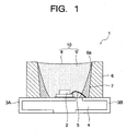
- Fig. 1 is a sectional view showing a structure of a white light-emitting lamp according to an embodiment of the invention.
- the white light-emitting lamp 1 shown in the figure is a white light-emitting LED lamp (white LED lamp) having a LED chip 2 having an emission wavelength in a range of 360 nm or more and 440 nm or less as a light source (exciting source).
- the light source of the white light-emitting lamp 1 is not limited to the LED chip 2 but may be a laser diode (semiconductor laser) or the like.
- a semiconductor light-emitting device having an emission wavelength of 360 nm or more and 440 nm or less is used.
- the LED chip 2 as the light source of the white LED lamp 1 is mounted on a wiring board 4 having a pair of lead terminals 3A, 3B.
- a lower electrode of the LED chip 2 is electrically and mechanically connected to the lead terminal 3A.
- An upper electrode of the LED chip 2 is electrically connected to the lead terminal 3B via a bonding wire 5.
- an ultraviolet emission LED which emits ultraviolet light or purple light having a wavelength in a range of 360 to 440 nm is used.
- a LED chip having a nitride based compound semiconductor layer as the light emission layer is exemplified. If the LED chip 2 has an emission wavelength not falling in the above-described range, white light having high luminance and high color rendering properties cannot be obtained. It is more desirable that the LED chip 2 has an emission wavelength in a range of 370 to 430 nm.
- a cylindrical resin frame 6 is disposed on the wiring board 4, and a reflection layer 7 is formed on its inner wall surface 6a.
- the resin frame 6 is filled with a transparent resin 8 as a resin layer, and the LED chip 2 is embedded in the transparent resin 8.
- the transparent resin 8 in which the LED chip 2 is embedded contains a white lamp phosphor (BGR phosphor) 9 including a blue light-emitting phosphor, a green light-emitting phosphor and a red light-emitting phosphor.
- BGR phosphor white lamp phosphor
- the phosphor 9 dispersed in the transparent resin 8 is excited by ultraviolet light or purple light which is emitted from the LED chip 2 to emit white light.
- the electrical energy applied to the white LED lamp 1 is converted to ultraviolet light or purple light by the LED chip 2, and the light is converted to light having a longer wavelength by the white light-emitting phosphor 9 dispersed into the transparent resin 8.
- the white light which is based on the white light-emitting phosphor 9 contained in the transparent resin 8 is emitted from the LED lamp 1.
- the transparent resin (resin layer) 8 containing the white light-emitting phosphor 9 functions as a light-emitting part 10 and is disposed at a front side in a light emission direction of the LED chip 2.
- the white LED lamp (white light-emitting lamp) 1 is configured of the above-described light-emitting part 10 and the LED chip 2 as the light source.
- the transparent resin 8 contained in the white light-emitting phosphor 9 for example, a silicone resin, an epoxy resin or the like can be used.
- the white light-emitting phosphor 9 is dispersed into the entire transparent resin 8.
- the white light-emitting phosphor 9 may be partially dispersed into the transparent resin 8.
- the white light-emitting phosphor 9 may contain supplementarily phosphors having emission colors other than blue, green and red.
- the individual phosphors of blue, green and red configuring the white light-emitting phosphor 9 it is desirable to use a phosphor which efficiently absorbs ultraviolet light or purple light having a wavelength in a range of 360 to 440 nm emitted from the LED chip 2.
- a phosphor which efficiently absorbs ultraviolet light or purple light having a wavelength in a range of 360 to 440 nm emitted from the LED chip 2.
- the blue light-emitting phosphor at least one selected from a europium (Eu)-activated halophosphate phosphor and a europium (Eu)-activated aluminate phosphor excelling in ultraviolet light or purple light absorption efficiency is used.
- Eu-activated halophosphate phosphor there is used, for example, a phosphor having a composition which is represented by the general formula: (M1 1-c , Eu c ) 10 (PO 4 ) 6 ⁇ Cl 2 (1) (where, M1 denotes at least one element selected from Mg, Ca, Sr and Ba, and c denotes a number meeting 0.005 ⁇ c ⁇ 0.03).
- Eu-activated aluminate phosphor there is used, for example, a phosphor having a composition which is represented by the general formula: m(M2 1-d , Eu d )O•nAl 2 O 3 (2) (where, M2 denotes at least one element selected from Mg, Ca, Sr, Ba and Zn, and d, m and n are numbers meeting 0.05 ⁇ d ⁇ 0.3, 0 ⁇ m, 0 ⁇ n, 0.2 ⁇ m/n ⁇ 1.5).
- red light-emitting phosphor at least one selected from a europium (Eu) and samarium (Sm)-activated lanthanum oxysulfide phosphor and a copper (Cu) and manganese (Mn)-activated zinc sulfide phosphor is used. These phosphors each can be used as the red luminescent component of the white LED lamp 1.
- Eu and Sm-activated lanthanum oxysulfide phosphor there is used, for example, a phosphor having a composition which is represented by the general formula: (La 1-a-b , Eu a , Sm b ) 2 O 2 S (3) (where, a and b are numbers meeting 0.01 ⁇ a ⁇ 0.15, 0.0001 ⁇ b ⁇ 0.03).
- the Cu and Mn-activated zinc sulfide phosphor there is used, for example, a phosphor having a composition which is represented by the general formula: ZnS : Cu v , Mn w (4) (where, v and ware numbers meeting 0.0002 ⁇ v ⁇ 0.001, 0.005 ⁇ w ⁇ 0.014).
- the red light-emitting phosphors represented by the formula (3) and the formula (4) each can be used as a red luminescent component which is emitted by ultraviolet light or purple light emitted from the LED chip 2.
- the red luminescent component Considering the emission properties (emission intensity etc.) of the red luminescent component, at least the Eu and Sm-activated lanthanum oxysulfide phosphor is preferably used as the red luminescent component.
- the red luminescent component is not enough, so that it is effective to use the Cu and Mn-activated zinc sulfide phosphor together.
- the red light-emitting phosphors represented by the formula (3) and the formula (4) are excellent in absorption efficiency of ultraviolet light or purple light having a wavelength in a range of 360 to 440 nm in comparison with another red light-emitting phosphor. But, they do not necessarily have a sufficient luminous efficiency in comparison with the blue light-emitting phosphor and the green light-emitting phosphor.
- the Eu and Sm-activated lanthanum oxysulfide phosphor and the Cu and Mn-activated zinc sulfide phosphor are used together to reinforce the red luminescent component but poor in luminous efficiency in comparison with the blue light-emitting phosphor and the green light-emitting phosphor.
- the white LED lamp 1 of this embodiment uses a green light-emitting phosphor containing a larger amount of a long wavelength component in comparison with a conventional green component.
- a gold (Au) and aluminum (Al)-activated zinc sulfide phosphor is used as a green light-emitting phosphor.
- the Au and A1-activated zinc sulfide phosphor there is used, for example, a phosphor having a composition which is represented by the general formula: ZnS:Au x , Al y (5) (where, x and y are numbers meeting 0.0002 ⁇ x ⁇ 0.0015, 0.0001 ⁇ y ⁇ 0.0012).
- the value x (molar ratio of Au to 1 mol of ZnS) in the formula (5) is less than 0.0002, desirable emission colors cannot be obtained because emission chromaticity is deviated toward blue. Meanwhile, if the value x exceeds 0.0015, a body color of the phosphor is deteriorated and luminance is lowered. If the value y (molar ratio of Al to 1 mol of ZnS) in the formula (5) is less than 0.0001, Au is prevented from being contained in the zinc sulfide, resulting in lowering the luminance. Meanwhile, if the value y exceeds 0.0012, the body color of the phosphor is deteriorated, resulting in lowering the luminance.
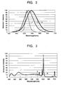
- Fig. 2 shows an emission spectrum (a) of the Au and Al-activated zinc sulfide phosphor (ZnS:Au, Al phosphor) in comparison with an emission spectrum (b) of a conventional Cu and Al-activated zinc sulfide phosphor (ZnS:Cu, Al phosphor) and an emission spectrum (c) of a Eu and Mn-activated aluminate phosphor (3(Ba, Mg, Eu, Mn)O ⁇ 8Al 2 O 3 phosphor). It is apparent from Fig.
- the zinc sulfide phosphor activated by Au and Al contains a large amount of a long wavelength component in comparison with the conventional Cu and Al-activated zinc sulfide phosphor and Eu and Mn-activated aluminate phosphor.
- the red luminescent component can be reinforced.
- the above-described white light-emitting phosphor 9 includes light of around 450 nm, around 560 nm and around 620 nm in good balance, so that color rendering properties of white light can be enhanced.
- a green light-emitting phosphor including the Au and Al-activated zinc sulfide phosphor (ZnS:Au, Al phosphor) containing a larger amount of a long wavelength component in comparison with a conventional green luminescent component is used, insufficient light emission due to the red light-emitting phosphor can be reinforced.
- the white LED lamp 1 which has both the high color rendering properties and high luminance balanced can be realized.
- Improvement effects of the luminance characteristics of the white LED lamp 1 by the green light-emitting phosphor can be obtained even when either the Eu and Sm-activated lanthanum oxysulfide phosphor or the Cu and Mn-activated zinc sulfide phosphor is used as the red light-emitting phosphor.
- a mixing ratio of the red light-emitting phosphors is desirably determined such that, for example, a mass ratio of the Eu and Sm-activated lanthanum oxysulfide phosphor and the Cu and Mn-activated zinc sulfide phosphor is in a range of 8:2 to 3 : 7 though variable depending on a color temperature of the target white light.
- Fig. 3 shows an example of an emission spectrum of the white LED lamp 1 using the three-color mixed phosphor 9 containing the above-described individual phosphors of blue, green and red.
- an emission spectrum [A] is an emission spectrum of the white LED lamp 1 using the Eu-activated halophosphate phosphor as the blue luminescent component, the Au and Al-activated zinc sulfide phosphor as the green luminescent component, and the Eu and Sm-activated lanthanum oxysulfide phosphor as the red luminescent component.
- An emission spectrum [B] is an emission spectrum of the white LED lamp 1 having the Cu and Mn-activated zinc sulfide phosphor added as the red luminescent component to the combination of the phosphors of the emission spectrum [A].
- the blue luminescent component has a peak value of 450 nm
- the green luminescent component has a peak value of 545 nm
- the red luminescent component has a peak value of 623 nm for both the phosphor combination [A] and the phosphor combination [B].
- the characteristic values including an average color rendering index of 90 or more and luminance of 300 mcd or more are obtained.
- the emission spectrum of the combination [B] has the luminescent component increased in a range around 580 nm and higher. It is because the Eu and Sm-activated lanthanum oxysulf ide phosphor and the Cu and Mn-activated zinc sulfide phosphor are used together for the red luminescent component. It is possible to enhance furthermore the luminance characteristics of the white LED lamp 1.
- the above-described individual phosphors of blue, green and red are dispersed into the transparent resin 8 as, for example, a mixture thereof.
- the individual phosphors are desired that their mixture has an average particle diameter of 7 ⁇ m or more.
- the average particle diameter indicates an median value (value of 50%) of a grain size distribution.
- the white light-emitting phosphor(three-color mixed phosphor) 9 which is a mixture of the individual phosphors of blue, green and red is determined to have an average particle diameter of 7 ⁇ m or more, so that the luminance of the white LED lamp 1 can be further improved.
- the three-color mixed phosphor 9 has desirably an average particle diameter of 8 ⁇ m or more.
- the upper limit of the average particle diameter of the three-color mixed phosphor 9 is not particularly limited but preferably 100 ⁇ m or less considering the formability and the like of the light-emitting part 10. If the average particle diameter of the three-color mixed phosphor 9 exceeds 100 ⁇ m, there is a possibility of causing problems that a flat surface is hardly obtained when its mixture with the transparent resin 8 is coated on the LED chip 2, and the like.
- the individual phosphors of blue, green and red may be integrated into one body by a binder such as an inorganic binder or an organic binder in advance and dispersed in the obtained state into the transparent resin 8 in order to improve the uniformity in the state dispersed into the transparent resin 8.
- a binder such as an inorganic binder or an organic binder in advance and dispersed in the obtained state into the transparent resin 8 in order to improve the uniformity in the state dispersed into the transparent resin 8.
- a pulverized alkaline earth borate or the like can be used as the inorganic binder, and a transparent resin such as an acrylic resin, a silicone resin or the like can be used as the organic binder.
- the inorganic binder or the organic binder is used to perform the integration processing, the individual phosphors are adhered at random to have a large particle diameter.
- the nonuniformity of the dispersed state of the individual phosphors in the transparent resin 8 due to a difference in settling rate or the like is remedied, so that the reproducibility of white light and the uniformity of light emission can be improved.
- the white light-emitting phosphor (integrated phosphor) 9 which is integrated by the binder is desirable that its average primary particle diameter is 7 ⁇ m or more before the integration, and its average secondary particle diameter is 10 ⁇ m or more after the integration. If the average secondary particle diameter is less than 10 ⁇ m, sufficient effects might not be obtained by the integration processing.
- the upper limit of the average secondary particle diameter of the integrated phosphor 9 is not particularly limited but desirably 100 ⁇ m or less considering the formability and the like of the light-emitting part 10. If the average secondary particle diameter of the integrated phosphor 9 exceeds 100 ⁇ m, there is a possibility of a problem that it is hard to form a flat surface on the LED chip 2 because of mixing with the transparent resin 8. The effect of improving the luminance based on the average particle diameter is also effective for the phosphor which has undergone the integration processing. Therefore, it is desirable that the individual phosphors before the integration are determined to have an average primary particle diameter of 7 ⁇ m or more.
- the white LED lamp 1 of this embodiment is used for, for example, the backlight of various types of displays, which are represented by a liquid crystal display, and various types of illuminating devices.
- the liquid crystal display provided with the backlight using the white LED lamp 1 can be applied to the display unit of various types of equipment such as portable communication devices, PC peripheral devices, office automation equipment, home electric appliances, and the like.
- the illuminating device using the white LED lamp 1 can be used as signal equipment, various types of switches, vehicle-mounted lamps, and also general illuminating devices and the like.
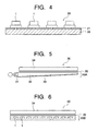
- Fig. 4 is a diagram showing an outline structure of the backlight according to an embodiment of the invention.
- a backlight 2 0 shown in the figure has plural white LED lamps 1 which are arranged in a linear or matrix form. These white LED lamps 1 are mounted on a substrate 22 which has a wiring layer 21, and the individual lead terminals of the white LED lamps 1 are electrically connected to the wiring layer 21. The plural white LED lamps 1 are sequentially connected in series.
- the light emitting device of the backlight 20 is not limited to the LED lamps 1, but a light emitting device which applies a semiconductor light-emitting device such as a laser diode to the light source can be used.
- the backlight 20 is applied to liquid crystal displays 30, 40 shown in, for example, Fig. 5 and Fig. 6 .
- the liquid crystal displays 30, 40 shown in these figures indicate embodiments of the liquid crystal display of the invention.
- Fig. 5 shows the liquid crystal display 30 applying a sidelight type backlight 20A.
- the sidelight type backlight 20A has an emission system 31 using the white LED lamp 1 and a light guide plate 32.
- the light guide plate 32 is determined to have a light incident portion at its one end where the light-emitting part 31 is disposed.
- the light guide plate 32 is tapered from the end having the light incident portion toward the other end, and a reflective layer 33 is disposed on the bottom surface of the tapered portion.
- Light radiated from the emission system 31 repeats refraction and reflection within the light guide plate 32 and is irradiated from the upper surface of the light guide plate 32 in its normal direction.
- a transmissive or semi-transmissive color liquid crystal display unit 34 is disposed on the side of the light emission surface of the sidelight type backlight 20A, thereby configuring the liquid crystal display 30.
- An optical sheet 35 such as a diffusion sheet, a reflection sheet or the like may be disposed between the sidelight type backlight 20A and the color liquid crystal display unit 34.
- Fig. 6 shows the liquid crystal display 40 applying a directly-beneath type backlight 20B.
- the directly-beneath type backlight 20B has the white LED lamps 1 which are arranged in a matrix form according to the shape and area of the transmissive or semi-transmissive color liquid crystal display unit 34.
- the color liquid crystal display unit 34 is disposed directly in the light emission direction of the plural white LED lamps 1 configuring the backlight 20B.
- the liquid crystal display 40 is comprised of the directly-beneath type backlight 20B and the color liquid crystal display unit 34 and, if necessary, the optical sheet 35 between them.
- the above-described blue light-emitting phosphor, green light-emitting phosphor and red light-emitting phosphor were weighed in 1.74g, 2.17g and 2. 33g and mixed by three rollers.
- the same is also applied to Examples 2 to 10 and Comparative Example 1 described below.
- the mixture of the individual phosphors had an average particle diameter (dispersion median diameter) of 9.5 ⁇ m.
- the obtained mixture phosphor was used to produce the white LED lamp 1 shown in Fig. 1 .
- the LED lamp 1 was produced as described below. First, the mixture phosphor in 30 mass% was added to and mixed with a silicone resin which forms the transparent resin 8 to prepare slurry. The slurry was dripped onto an ultraviolet emission LED chip 2 having an emission peak wavelength of 400 nm and a shape of 300 ⁇ m square, and the silicone resin was cured at 140°C. Thus, the ultraviolet emission LED chip 2 was sealed with the silicone resin containing the mixture phosphor (mixture phosphor of blue, green and red). The obtained white LED lamp was subjected to the characteristic evaluation to be described later.
- the same phosphors in the same amounts as in Example 1 were prepared and integrated into one body by the method described below.
- the integrating step to the individual phosphors were added an acrylic resin emulsion at a ratio of 0.1 mass% in solid content ratio to the phosphor, and they were mixed. Then, the mixture was dried at 120°C and sieved with a nylon mesh to obtain an integrated phosphor. An average primary particle diameter before the integration was 9.5 ⁇ m, and the average secondary particle diameter after the integration was 17.6 ⁇ m.
- the integrated phosphor was used to produce a white LED lamp in the same manner as in Example 1. The produced white LED lamp was subjected to the characteristic evaluation to be described later.
- aCu and Mn-activated zinc sulfide (ZnS:Cu 0.0005 , Mn 0.008 ) phosphor was prepared as a red light-emitting phosphor.
- a Eu-activated alkali earth chlorophosphate, an Au and Al-activated zinc sulfide phosphor, a Eu and Sm-activated lanthanum oxysulfide phosphor and a Cu and Mn-activated zinc sulfide phosphor were weighed in 2.10g, 2.22g, 2.10g and 0.82g. They were mixed in the same manner as in Example 1.
- the mixture of the individual phosphors had an average particle diameter of 9.8 ⁇ m.
- the mixed phosphor was used to produce a white LED lamp in the same manner as in Example 1. The produced white LED lamp was subjected to the characteristic evaluation to be described later.
- Example 1 Mixed phosphors or integrated phosphors were produced in the same manner as in Example 1 or Example 2 except that the combination of blue, green and red light-emitting phosphors shown in Table 1 was applied.
- the individual mixed phosphors or integrated phosphors were used to produce white LED lamps in the same manner as in Example 1.
- the produced white LED lamps were subjected to the characteristic evaluation to be described later.
- the blue light-emitting phosphor, the green light-emitting phosphor and the red light-emitting phosphor were weighed in 1.44g, 1.49g and 3.32g, and they were mixed by three rollers.
- the mixed phosphor was used to produce a white LED lamp in the same manner as in Example 1.
- the produced lamp was subjected to the characteristic evaluation to be described later.
- the blue light-emitting phosphor, the green light-emitting phosphor and the red light-emitting phosphor were weighed in 2.71g, 0.45g and 1.85g, and they were mixed by three rollers.
- the mixed phosphor was used to produce a white LED lamp in the same manner as in Example 1.
- the produced lamp was subjected to the characteristic evaluation to be described later.
- Electric current of 20 mA was passed to the individual white LED lamps of Examples 1 to 11 and Comparative Examples 1 and 2 described above to illuminate them, and the individual white LED lamps were measured for emission luminance, average color rendering index, and chromaticity. The measured results are shown in Table 3.
- the individual white LED lamps were measured for the emission property by a CAS 140B COMPACT ARRAY SPECTROMETER produced by Instrument Systems and MCPD equipment produced by OTSUKA ELECTRONICS CO., LTD.
- the white light-emitting lamp of the invention uses a gold and aluminum-activated zinc sulfide phosphor which contains a larger amount of a long wavelength component as a green light-emitting phosphor, so that the luminescent component based on the red light-emitting phosphor can be reinforced.
- the luminance characteristics can be improved without impairing the inherent high color rendering properties of the white light-emitting lamp using the ultraviolet emission LED.
- the white light-emitting lamp having achieved both the high color rendering properties and the high luminance can be used effectively for various usages.
Landscapes
- Chemical & Material Sciences (AREA)
- Engineering & Computer Science (AREA)
- Physics & Mathematics (AREA)
- Inorganic Chemistry (AREA)
- Materials Engineering (AREA)
- Organic Chemistry (AREA)
- General Physics & Mathematics (AREA)
- Optics & Photonics (AREA)
- Nonlinear Science (AREA)
- Microelectronics & Electronic Packaging (AREA)
- Mathematical Physics (AREA)
- Crystallography & Structural Chemistry (AREA)
- Manufacturing & Machinery (AREA)
- Computer Hardware Design (AREA)
- Power Engineering (AREA)
- Luminescent Compositions (AREA)
- Led Device Packages (AREA)
Applications Claiming Priority (2)
| Application Number | Priority Date | Filing Date | Title |
|---|---|---|---|
| JP2005070322 | 2005-03-14 | ||
| PCT/JP2006/303418 WO2006098132A1 (ja) | 2005-03-14 | 2006-02-24 | 白色発光ランプとそれを用いたバックライト、表示装置および照明装置 |
Publications (3)
| Publication Number | Publication Date |
|---|---|
| EP1860173A1 EP1860173A1 (en) | 2007-11-28 |
| EP1860173A4 EP1860173A4 (en) | 2012-07-04 |
| EP1860173B1 true EP1860173B1 (en) | 2013-12-25 |
Family
ID=36991485
Family Applications (1)
| Application Number | Title | Priority Date | Filing Date |
|---|---|---|---|
| EP06714557.3A Active EP1860173B1 (en) | 2005-03-14 | 2006-02-24 | White light-emitting lamp, backlight using same, display and illuminating device |
Country Status (7)
| Country | Link |
|---|---|
| US (1) | US7857992B2 (ja) |
| EP (1) | EP1860173B1 (ja) |
| JP (1) | JP4945436B2 (ja) |
| KR (1) | KR100892800B1 (ja) |
| CN (1) | CN101137737B (ja) |
| TW (1) | TW200644286A (ja) |
| WO (1) | WO2006098132A1 (ja) |
Families Citing this family (17)
| Publication number | Priority date | Publication date | Assignee | Title |
|---|---|---|---|---|
| JP4965840B2 (ja) * | 2005-09-29 | 2012-07-04 | 株式会社東芝 | 白色発光型ledランプの製造方法およびそれを用いたバックライトの製造方法並びに液晶表示装置の製造方法 |
| WO2008126023A2 (en) * | 2007-04-16 | 2008-10-23 | Koninklijke Philips Electronics N.V. | Optical arrangement |
| US9279079B2 (en) * | 2007-05-30 | 2016-03-08 | Sharp Kabushiki Kaisha | Method of manufacturing phosphor, light-emitting device, and image display apparatus |
| KR100858641B1 (ko) * | 2008-01-08 | 2008-09-16 | 유항재 | 시력 보호 기능을 가진 컴팩트 형광램프용 아답터 |
| CN101769506B (zh) * | 2009-01-05 | 2011-08-24 | 王伟立 | 一种制作纯白光二极管光源的方法 |
| KR101588314B1 (ko) | 2009-09-25 | 2016-01-25 | 삼성전자주식회사 | 형광체, 이를 포함하는 백색발광소자 및 형광체 제조방법 |
| EP2540798A4 (en) * | 2010-02-26 | 2014-04-30 | Mitsubishi Chem Corp | Halophosphate Phosphorus and White Light Output Device |
| CN101899308B (zh) * | 2010-06-25 | 2013-01-02 | 海洋王照明科技股份有限公司 | 掺杂金属纳米粒子的稀土铝酸镧发光材料及其制备方法 |
| CN102163536A (zh) * | 2011-05-25 | 2011-08-24 | 扬州虹扬光电有限公司 | 一种发出绿色光的荧光辉光灯 |
| JP5872828B2 (ja) * | 2011-09-28 | 2016-03-01 | 株式会社小糸製作所 | 発光モジュールおよび蛍光体 |
| CN103289702B (zh) * | 2013-06-27 | 2014-11-05 | 苏州大学 | 一种氟磷酸盐基红色荧光粉、制备方法及应用 |
| DE102014018586A1 (de) * | 2014-12-17 | 2016-06-23 | Merck Patent Gmbh | Lasermarkierbare und laserschweißbare polymere Materialien |
| CN104880759B (zh) * | 2015-05-19 | 2019-02-26 | 武汉华星光电技术有限公司 | 背光单元及显示装置 |
| EP3321342B1 (en) * | 2015-07-07 | 2020-08-05 | Dyden Corporation | Blue-green-light-emitting phosphor, light-emitting element, light-emitting device, and white-light-emitting device |
| DE102016115523A1 (de) * | 2016-08-22 | 2018-02-22 | Osram Gmbh | Gasentladungslampe und Scheinwerfersystem mit Gasentladungslampe |
| EP3576168B1 (en) | 2018-05-31 | 2023-05-31 | Nichia Corporation | Light emitting device |
| CN116925765B (zh) * | 2023-07-18 | 2024-05-07 | 西华大学 | 一种钪铝酸盐光致变色可逆上转换发光荧光粉材料及其调制的方法 |
Family Cites Families (4)
| Publication number | Priority date | Publication date | Assignee | Title |
|---|---|---|---|---|
| JP3949290B2 (ja) * | 1998-08-31 | 2007-07-25 | 株式会社東芝 | 表示装置 |
| WO2004031322A1 (ja) * | 2002-09-30 | 2004-04-15 | Kabushiki Kaisha Toshiba | 表示装置用蛍光体とその製造方法、およびそれを用いたカラー表示装置 |
| JP4233929B2 (ja) * | 2003-05-09 | 2009-03-04 | 化成オプトニクス株式会社 | 蛍光体とそれを用いた発光素子 |
| US7935975B2 (en) * | 2005-09-29 | 2011-05-03 | Kabushiki Kaisha Toshiba | White LED lamp and backlight using the same, and liquid crystal display device using the backlight |
-
2006
- 2006-02-24 JP JP2007508050A patent/JP4945436B2/ja active Active
- 2006-02-24 KR KR1020077023428A patent/KR100892800B1/ko active IP Right Grant
- 2006-02-24 WO PCT/JP2006/303418 patent/WO2006098132A1/ja active Application Filing
- 2006-02-24 EP EP06714557.3A patent/EP1860173B1/en active Active
- 2006-02-24 US US11/908,611 patent/US7857992B2/en active Active
- 2006-02-24 CN CN2006800078692A patent/CN101137737B/zh active Active
- 2006-03-01 TW TW095106841A patent/TW200644286A/zh unknown
Also Published As
| Publication number | Publication date |
|---|---|
| CN101137737B (zh) | 2011-03-23 |
| JP4945436B2 (ja) | 2012-06-06 |
| CN101137737A (zh) | 2008-03-05 |
| EP1860173A4 (en) | 2012-07-04 |
| KR20070111553A (ko) | 2007-11-21 |
| KR100892800B1 (ko) | 2009-04-10 |
| TW200644286A (en) | 2006-12-16 |
| US20090026916A1 (en) | 2009-01-29 |
| WO2006098132A1 (ja) | 2006-09-21 |
| TWI299217B (ja) | 2008-07-21 |
| EP1860173A1 (en) | 2007-11-28 |
| JPWO2006098132A1 (ja) | 2008-08-21 |
| US7857992B2 (en) | 2010-12-28 |
Similar Documents
| Publication | Publication Date | Title |
|---|---|---|
| EP1860173B1 (en) | White light-emitting lamp, backlight using same, display and illuminating device | |
| US7961762B2 (en) | White light-emitting lamp and illuminating device using the same | |
| JP5127455B2 (ja) | 白色発光装置とその製造方法、およびそれを用いたバックライト並びに液晶表示装置 | |
| EP1796181B1 (en) | Light emitting device, and back light and liquid crystal display employing it | |
| KR101331304B1 (ko) | 백색 발광 램프 및 그것을 포함하는 백색 led 조명 장치 | |
| US8710532B2 (en) | White light emitting lamp and white LED lighting apparatus including the same | |
| US7935975B2 (en) | White LED lamp and backlight using the same, and liquid crystal display device using the backlight | |
| US7859182B2 (en) | Warm white LED-based lamp incoporating divalent EU-activated silicate yellow emitting phosphor | |
| JP4965840B2 (ja) | 白色発光型ledランプの製造方法およびそれを用いたバックライトの製造方法並びに液晶表示装置の製造方法 | |
| US20080067918A1 (en) | Light emitting module |
Legal Events
| Date | Code | Title | Description |
|---|---|---|---|
| PUAI | Public reference made under article 153(3) epc to a published international application that has entered the european phase |
Free format text: ORIGINAL CODE: 0009012 |
|
| 17P | Request for examination filed |
Effective date: 20070911 |
|
| AK | Designated contracting states |
Kind code of ref document: A1 Designated state(s): DE NL |
|
| DAX | Request for extension of the european patent (deleted) | ||
| RBV | Designated contracting states (corrected) |
Designated state(s): DE NL |
|
| A4 | Supplementary search report drawn up and despatched |
Effective date: 20120604 |
|
| RIC1 | Information provided on ipc code assigned before grant |
Ipc: C09K 11/64 20060101AFI20120529BHEP Ipc: H01L 33/00 20100101ALI20120529BHEP Ipc: F21V 9/00 20060101ALI20120529BHEP Ipc: G02F 1/13357 20060101ALI20120529BHEP Ipc: G02F 1/1335 20060101ALI20120529BHEP Ipc: C09K 11/84 20060101ALI20120529BHEP Ipc: C09K 11/73 20060101ALI20120529BHEP Ipc: G02B 6/00 20060101ALI20120529BHEP |
|
| GRAP | Despatch of communication of intention to grant a patent |
Free format text: ORIGINAL CODE: EPIDOSNIGR1 |
|
| INTG | Intention to grant announced |
Effective date: 20130419 |
|
| GRAP | Despatch of communication of intention to grant a patent |
Free format text: ORIGINAL CODE: EPIDOSNIGR1 |
|
| GRAS | Grant fee paid |
Free format text: ORIGINAL CODE: EPIDOSNIGR3 |
|
| INTG | Intention to grant announced |
Effective date: 20130904 |
|
| GRAA | (expected) grant |
Free format text: ORIGINAL CODE: 0009210 |
|
| AK | Designated contracting states |
Kind code of ref document: B1 Designated state(s): DE NL |
|
| REG | Reference to a national code |
Ref country code: DE Ref legal event code: R096 Ref document number: 602006039763 Country of ref document: DE Effective date: 20140220 |
|
| REG | Reference to a national code |
Ref country code: NL Ref legal event code: T3 |
|
| REG | Reference to a national code |
Ref country code: DE Ref legal event code: R097 Ref document number: 602006039763 Country of ref document: DE |
|
| PLBE | No opposition filed within time limit |
Free format text: ORIGINAL CODE: 0009261 |
|
| STAA | Information on the status of an ep patent application or granted ep patent |
Free format text: STATUS: NO OPPOSITION FILED WITHIN TIME LIMIT |
|
| 26N | No opposition filed |
Effective date: 20140926 |
|
| REG | Reference to a national code |
Ref country code: DE Ref legal event code: R097 Ref document number: 602006039763 Country of ref document: DE Effective date: 20140926 |
|
| REG | Reference to a national code |
Ref country code: DE Ref legal event code: R081 Ref document number: 602006039763 Country of ref document: DE Owner name: TOSHIBA MATERIALS CO., LTD., YOKOHAMA-SHI, JP Free format text: FORMER OWNERS: KABUSHIKI KAISHA TOSHIBA, TOKIO/TOKYO, JP; TOSHIBA MATERIALS CO., LTD., YOKOHAMA-SHI, KANAGAWA, JP |
|
| REG | Reference to a national code |
Ref country code: NL Ref legal event code: PD Owner name: TOSHIBA MATERIALS CO., LTD.; JP Free format text: DETAILS ASSIGNMENT: CHANGE OF OWNER(S), ASSIGNMENT; FORMER OWNER NAME: TOSHIBA MATERIALS CO., LTD. Effective date: 20210916 |
|
| REG | Reference to a national code |
Ref country code: NL Ref legal event code: PD Owner name: SEOUL SEMICONDUCTOR CO.,LTD.; KO Free format text: DETAILS ASSIGNMENT: CHANGE OF OWNER(S), ASSIGNMENT; FORMER OWNER NAME: TOSHIBA MATERIALS CO., LTD. Effective date: 20211207 |
|
| PGFP | Annual fee paid to national office [announced via postgrant information from national office to epo] |
Ref country code: NL Payment date: 20231206 Year of fee payment: 19 |
|
| PGFP | Annual fee paid to national office [announced via postgrant information from national office to epo] |
Ref country code: DE Payment date: 20231205 Year of fee payment: 19 |