EP1857849A1 - Optical transmission module and method of manufacturing the same - Google Patents
Optical transmission module and method of manufacturing the same Download PDFInfo
- Publication number
- EP1857849A1 EP1857849A1 EP06023372A EP06023372A EP1857849A1 EP 1857849 A1 EP1857849 A1 EP 1857849A1 EP 06023372 A EP06023372 A EP 06023372A EP 06023372 A EP06023372 A EP 06023372A EP 1857849 A1 EP1857849 A1 EP 1857849A1
- Authority
- EP
- European Patent Office
- Prior art keywords
- optical
- support member
- transmission module
- mounting support
- section
- Prior art date
- Legal status (The legal status is an assumption and is not a legal conclusion. Google has not performed a legal analysis and makes no representation as to the accuracy of the status listed.)
- Withdrawn
Links
- 230000003287 optical effect Effects 0.000 title claims abstract description 240
- 230000005540 biological transmission Effects 0.000 title claims abstract description 71
- 238000004519 manufacturing process Methods 0.000 title claims description 16
- 239000013307 optical fiber Substances 0.000 claims abstract description 61
- 239000000758 substrate Substances 0.000 claims abstract description 22
- 230000007246 mechanism Effects 0.000 claims abstract description 9
- 238000006243 chemical reaction Methods 0.000 claims abstract description 8
- 238000000465 moulding Methods 0.000 claims description 10
- 239000011347 resin Substances 0.000 claims description 9
- 229920005989 resin Polymers 0.000 claims description 9
- 239000000835 fiber Substances 0.000 claims description 7
- 238000007789 sealing Methods 0.000 claims description 3
- 238000000034 method Methods 0.000 description 10
- 238000010586 diagram Methods 0.000 description 8
- 230000000694 effects Effects 0.000 description 8
- 238000003780 insertion Methods 0.000 description 6
- 230000037431 insertion Effects 0.000 description 6
- 238000013459 approach Methods 0.000 description 5
- 238000010276 construction Methods 0.000 description 5
- 230000008859 change Effects 0.000 description 3
- 230000008569 process Effects 0.000 description 3
- 230000009467 reduction Effects 0.000 description 3
- 238000001125 extrusion Methods 0.000 description 2
- 239000000463 material Substances 0.000 description 2
- 238000009792 diffusion process Methods 0.000 description 1
- 238000012986 modification Methods 0.000 description 1
- 230000004048 modification Effects 0.000 description 1
- 238000007639 printing Methods 0.000 description 1
Images





Classifications
-
- G—PHYSICS
- G02—OPTICS
- G02B—OPTICAL ELEMENTS, SYSTEMS OR APPARATUS
- G02B6/00—Light guides; Structural details of arrangements comprising light guides and other optical elements, e.g. couplings
- G02B6/24—Coupling light guides
- G02B6/42—Coupling light guides with opto-electronic elements
-
- G—PHYSICS
- G02—OPTICS
- G02B—OPTICAL ELEMENTS, SYSTEMS OR APPARATUS
- G02B6/00—Light guides; Structural details of arrangements comprising light guides and other optical elements, e.g. couplings
- G02B6/24—Coupling light guides
- G02B6/42—Coupling light guides with opto-electronic elements
- G02B6/4201—Packages, e.g. shape, construction, internal or external details
- G02B6/4219—Mechanical fixtures for holding or positioning the elements relative to each other in the couplings; Alignment methods for the elements, e.g. measuring or observing methods especially used therefor
- G02B6/4228—Passive alignment, i.e. without a detection of the degree of coupling or the position of the elements
- G02B6/423—Passive alignment, i.e. without a detection of the degree of coupling or the position of the elements using guiding surfaces for the alignment
-
- G—PHYSICS
- G02—OPTICS
- G02B—OPTICAL ELEMENTS, SYSTEMS OR APPARATUS
- G02B6/00—Light guides; Structural details of arrangements comprising light guides and other optical elements, e.g. couplings
- G02B6/24—Coupling light guides
- G02B6/42—Coupling light guides with opto-electronic elements
- G02B6/4201—Packages, e.g. shape, construction, internal or external details
- G02B6/4249—Packages, e.g. shape, construction, internal or external details comprising arrays of active devices and fibres
-
- G—PHYSICS
- G02—OPTICS
- G02B—OPTICAL ELEMENTS, SYSTEMS OR APPARATUS
- G02B6/00—Light guides; Structural details of arrangements comprising light guides and other optical elements, e.g. couplings
- G02B6/24—Coupling light guides
- G02B6/42—Coupling light guides with opto-electronic elements
- G02B6/43—Arrangements comprising a plurality of opto-electronic elements and associated optical interconnections
Definitions
- the present invention relates to an optical transmission module and a method of manufacturing the same, particularly an optical transmission module in which positioning between a photoelectric element and an optical fiber can be achieved precisely and easily, and reduction in size and cost can be realized.
- a conventional optical transmission module is provided with a plurality of photoelectric elements such as light emitting elements or light receiving elements.
- photoelectric elements such as light emitting elements or light receiving elements.
- positioning of the photoelectric element and an optical fiber has been a serious problem.
- the photoelectric element When one photoelectric element is provided, the photoelectric element is housed in a metallic can package such as a TO (Transistor Outline) can package, and a so-called active alignment is performed in which positioning between the photoelectric element and an optical fiber receptacle section is performed in a state where the photoelectric element emits light or receives light.
- a metallic can package such as a TO (Transistor Outline) can package
- an optical transmission module having a plurality of photoelectric elements In an optical transmission module having a plurality of photoelectric elements, a problem of positioning becomes more important.
- a positioning member such as a guide pin is used, so that an optical fiber, an optical receptacle, a photoelectric conversion section, and the photoelectric elements are positioned with respect to the guide pin (for example, refer to JP-A-2000-199838 ).
- an intermediate positioning member is further added so as to perform positioning.
- each part In the method disclosed in Patent Document 2, the respective parts are precisely positioned with respect to the guide pin. Therefore, each part needs to have a hole formed with high precision and at a certain depth, the hole passing through the guide pin. Accordingly, a manufacturing cost of each part becomes high. Further, the thickness of each part and a housing section of the pin are provided, thereby preventing miniaturization of the module.
- An object of the present invention is that it provides an optical transmission module and a method of manufacturing the same.
- the optical transmission module positioning between a photoelectric element and an optical fiber can be achieved precisely and easily, and reduction in size and cost can be realized.
- one embodiment of the invention provides the following optical transmission module and the method of manufacturing the same.
- the optical transmission module and the method of manufacturing the same, in which the positioning of the photoelectric element and the optical fiber can be realized precisely and easily, and the miniaturization and cost reduction can be achieved.
- Fig. 1 is a sectional view illustrating the construction of an optical transmission module according to a first embodiment of the invention.
- the optical transmission module 1 includes a mounting support member 11A, a plurality of photoelectric elements 12, and an optical part 13A.
- the mounting support member 11A is provided on an electric wiring section 21 disposed on a substrate 2.
- the electric wiring section 21 is an electric wiring part such as a printed circuit board, a flexible printed circuit board, a lead frame wiring lines or the like.
- the electric wiring section 21 is disposed on the substrate 2 in advance.
- the mounting support member 11A makes it possible to dispose the photoelectric element 12 in an optimal position on the electric wiring section 21 and to install the optical part 13A in an optimal position in the positional relationship with the photoelectric element 12.
- the mounting support member 11A is provided with a plurality of element positioning sections 111 and a plurality of optical part positioning sections 112.
- the element positioning section 111 is used in positioning for disposing the photoelectric element 12 on an optimal position of the electric wiring section 21, in order to connect the photoelectric element 12 to the electric wiring section 21.
- the optical part positioning section 112 is a convex portion (first convex portion) provided on the upper surface of the mounting support member 11A.
- the optical part positioning section 112 is fitted into a concave portion (second concave portion) 13a provided in the optical part 13A, so that the optical part 13A can be fixed in a suitable position.
- the photoelectric element 12 is a light emitting element such as a light emitting diode or surface emitting laser, which converts an electric signal into an optical signal.
- the photoelectric element 12 When receiving an electric signal delivered through the electric wiring section 21, the photoelectric element 12 emits a corresponding optical signal to deliver to optical fiber (not shown) through the optical part 13A.
- the photoelectric element 12 may be a light receiving element, such as a photodiode, which receives an optical signal emitted from the optical fiber (not shown) through the optical part 13A and converts the optical signal into an electrical signal to return.
- light emitting elements and light receiving elements may be used as for the plurality of photoelectric elements 12 on the substrate 2.
- a light emitting element such as surface emitting laser, or a light receiving element is used.
- any element, which performs photoelectric conversion may be used.
- the optical part 13A includes a plurality of lens sections 131 and an optical fiber receptacle section 132.
- the optical part 13A has a function of effectively delivering an optical signal emitted from the photoelectric element 12 to the optical fiber 4.
- the lens section 131 condenses optical signals, which are diffusely emitted from the photoelectric element 12, and performs photoelectric conversion so that the optical signals effectively enter the optical fiber.
- the lens section condenses optical signals, which are diffusely emitted from the optical fiber, and performs photoelectric conversion so that the optical signals are effectively condensed and received into the photoelectric element 12.
- the optical fiber receptacle section 132 fits and fixes one end of a fiber holder 3A holding the optical fiber 4 delivering an optical signal to an optimal position so that an optical signal emitted from the photoelectric element 12 is effectively received and an optical signal received in the photoelectric element 12 is effectively transmitted.
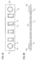
- Figs. 2A and 2B are diagrams illustrating the detailed structure of the mounting support member according to the first embodiment.
- Fig. 2A is a top view of the mounting support member 11A and Fig. 2B is a sectional view taken along an A-A line of Fig. 2A.
- the mounting support member 11A is a thin plate member having a substantially rectangular shape.
- the optical part positioning section 112 having a convex shape is provided on either side of the mounting support member 11A in a longitudinal direction. Between two of the optical part positioning sections 112, the plurality (four in Fig. 2) of element positioning sections 111 are provided, having a width for positioning a width direction of the photoelectric element 12.
- the element positioning section 111 is a hole provided through the plane-shaped mounting support member 11A.
- the mounting support member 11A is disposed on the electric wiring section 21, the electric wiring section 21 is exposed through the element positioning section 111 without being covered by the mounting support member 11A. Therefore, when the photoelectric element 12 is disposed in the element positioning section 111, the electric connection between the photoelectric element 12 and the electric wiring section 21 can be achieved.
- the wall surface of the element positioning section 111 is formed with an inclined surface 111a. Therefore, when the photoelectric element 12 is mounted, mechanical interference hardly occurs. Such a structure makes mounting easy.
- a taper 112a is formed at the side of the optical part positioning section 112 so that the optical part 13A is easily fitted.
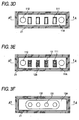
- Figs. 3A to 3F are diagrams illustrating a process of manufacturing an optical transmission module according to the first embodiment of the invention.
- Figs. 3B, 3D, and 3F are sectional views taken along an A-A line of Figs. 3A, 3C, and 3E, respectively.
- the electric wiring section 21 is disposed on the substrate 2. Then, the mounting support member 11A is positioned and fixed in accordance with an electrode pattern of the electric wiring section 21 and other positional information, as shown in Figs. 3A and 3B.
- the electric wiring section 21 is directly disposed on the substrate 2, for example, by a method of printing a circuit board on the substrate 2.
- the mounting support member 11A can be formed in a desired shape by resin molding, such as extrusion, or a cutting.
- the mounting support member 11A is used for determining an absolute position of the photoelectric element 12 with respect to the electric wiring section 21.
- an absolute position of the photoelectric element 12 with respect to the electric wiring section 21 has a relatively high degree of freedom. Therefore, the mounting precision of the mounting support member 11A with respect to the electric wiring section 21 may be relatively low, and mounting can be performed at a low cost.
- the plurality of photoelectric elements 12 are disposed using the element positioning section 111 of the mounting support member 11A and fixed to the electric wiring section 21.
- the width of one side of the element positioning section 111 composed of a substantially rectangular hole slightly exceeds that of the photoelectric element 12. Further, the photoelectric element 12 is disposed in accordance with the element positioning section of the mounting support member 11A, so that the photoelectric element 12 can be easily disposed in a desired position.
- the width of the other side of the element positioning section 111 is relatively larger than that of photoelectric element 12. This is because a space required for connecting an electrode provided on the photoelectric element 12 and the electric wiring section 21 through wire-bonding using wire 12a should be secured.
- the mounting support member 11A is preferably formed of a material having resistance to the heat.
- the wall surface of the element positioning section 111 is inclined, so that the size of the hole at the upper portion becomes larger than that of the hole at the lower portion, which makes it easy to dispose the photoelectric element 12.
- the optical part 13A is disposed on the mounting support member 11A.
- the disposed position of the optical part 13A is determined using two of the optical part positioning sections 112 of the mounting support member 11A.
- the plurality of lens sections 131 of the optical part 13 are respectively positioned on the corresponding photoelectric elements 12. That is, the plurality of lens sections 131 can be disposed in suitable positions.
- the optical part positioning section 112 is provided with the taper 112a so that the optical part 13A is easily fitted into the optical part positioning section 112. Therefore, when the optical part 13A is positioned with respect to the mounting support member 11A, mechanical interference hardly occurs. Such a structure makes mounting easy.
- the optical part 13A can be also formed in a desired shape by resin molding, such as extrusion, or a cutting.
- the photoelectric element 12 and the optical part 13A are directly positioned with respect to the mounting support member 11A. Therefore, without an intermediate member such as a guide pin, positioning with high precision can be realized. Further, since the thickness of the mounting support member 11A can be set to the thickness level of the photoelectric element 12, the mounting support member can be manufactured at a low cost.
- optical fiber receptacle 132 positioning of the optical fiber can be realized without an intermediate member such as a guide pin.
- An optical transmission module has alignment marks provided in a mounting support member, and the alignment marks are used for determining the disposed position of the photoelectric element 12.
- Figs. 4A and 4B are diagrams illustrating the structure of the mounting support member according to the second embodiment of the invention.
- Fig. 4A is a top view of the mounting support member 11B
- Fig. 4B is a sectional view taken along a line A-A of Fig. 4A.
- the mounting support member 11B according to the second embodiment has something in common with the mounting support member 11A according to the first embodiment in that the mounting support member 11B is a slim plate member having a substantially rectangular shape, the convex-shaped optical part positioning section 112 is provided on either side of the mounting support member 11B in the longitudinal direction, and the plurality of element positioning sections 111 are provided between two of the optical part positioning sections 112.
- the mounting support member 11B is different from the mounting support member 11A in that the alignment marks 113 are provided around each element positioning section 111.
- the alignment marks 113 are provided around the plurality of element positioning sections 111 of the mounting support member 11B.
- the alignment mark is a straight-line mark provided around the element positioning section 111 and is a concave portion, which is provided in advance when the mounting support member 11B is molded.
- the plurality of alignment marks 113 are provided around each of the element positioning sections 111. Optical positioning is performed such that a point, where the respective alignment marks 113 intersect each other when they are extended, overlaps the center of the optical element 12. Then, the absolute position of the optical element 12 is determined.
- the width of the element positioning section 111 in the mounting support member 11B may be relatively larger than that of the optical element 12. Further, the wall surface of the element positioning section 111 does not have to be formed with the inclined surface 111a.
- the photoelectric element 12 and the optical part 13A are directly positioned with respect to the mounting support member 11B. Therefore, without an intermediate member such as a guide pin, positioning with high precision can be realized.
- An optical transmission module has one array positioning section provided in a mounting support member. The disposed position of an element array including a plurality of photoelectric elements is determined by the array positioning section.
- Figs. 5A and 5B are diagrams illustrating the structure of the mounting support member according to the third embodiment of the invention.
- Fig. 5A is a top view of the mounting support member 11C
- the Fig. 5B is a sectional view taken along a line A-A of Fig. 5A.
- Figs. 5A and 5B shows the element array 14 disposed inside the array positioning section 114.
- one array positioning section 114 and a plurality (for example, two) of optical part positioning sections 112 are provided in the mounting support member 11C.
- the array positioning section 114 is used in positioning for disposing the element array 14 on an optimal position of the electric wiring section 21, in order to connect the element array 14 including the plurality of photoelectric elements to the electric wiring section 21.
- the element array 14 is where a plurality of photoelectric elements converting an electric signal into an optical signal are arranged.
- the element array 14 emits a corresponding optical signal to deliver to the optical fiber 4 (not shown) through the optical part 13A.
- the respective photoelectric elements receive an optical signal emitted from the optical fiber 4 (not shown) through the optical part 13A and return the optical signal into an electric signal.
- a light emitting element such as surface emitting laser or a light receiving element is used.
- any element which performs photoelectric conversion may be used.
- the mounting support member 11C is a slim plate member having a substantially rectangular shape.
- the convex-shaped optical part positioning section 112 is provided on either side of the mounting support member 11C in a longitudinal direction. Further, between two of the optical part positioning sections 112, one rectangular array positioning section 114 is provided.
- the array positioning section 114 is a hole provided in the plane mounting support member 11C.
- the mounting support member 11C is disposed on the electric wiring section 21, the electric wiring section 21 is exposed through the array positioning section 114 without being covered by the mounting support member 11C. Therefore, when the element array 14 is disposed in the array positioning section 114, the electric connection between the element array 14 and the electric wiring section 21 can be achieved.
- the wall surface of the array positioning section 114 is formed with an inclined surface 114a.
- alignment marks are not used in positioning the element array 14.
- alignment marks may be used for positioning the element array 14.
- the element array 14 and the optical part 13A are directly positioned with respect to the mounting support member 11C. Therefore, without an intermediate member such as a guide pin, positioning with high precision can be realized.
- An optical transmission module has a plurality of guide pins provided in the side of an optical fiber receptacle provided in an optical part.
- the guide pin is used for the connection between the optical part and the optical fiber.
- Fig. 6 is a sectional view illustrating the structure of the optical transmission module according to the fourth embodiment of the invention.
- the optical transmission module 1 includes a mounting support member 11A, a plurality of photoelectric elements 12, the optical part 13B, and the plurality of guide pins 15.
- the mounting support member 11A is provided on the electric wiring section 21 disposed on the substrate 2.
- the mounting support member 11A and the photoelectric elements 12 are the same as those of the first embodiment.
- the optical part 13B includes a plurality of lens sections 131, the optical fiber receptacle section 132, and a plurality of guide pin insertion holes (third concave portions) 133.
- the optical part 13B has a function of effectively delivering an optical signal emitted from the photoelectric element 12 to the optical fiber.
- the lens section 131 and the optical fiber receptacle section 132 are the same as those of the optical part 13A according to the first embodiment and have the same function.
- the guide pin insertion hole 133 is provided at the upper surface of the optical part 13B and at the side of the optical fiber receptacle section 132.
- the guide pin 15 is inserted into the guide pin insertion hole 133.
- the guide pin 15 After being inserted into the guide pin insertion hole 133, the guide pin 15 is used for connecting the optical fiber 4 (not shown) to the optical fiber receptacle section 132.
- a fitting section 3b of the fiber holder 3B holding the plurality of optical fibers 4 is fitted into the optical fiber receptacle 132, and the guide pin 15 is inserted into a pin hole 3a.
- the fitting section 3b When the guide pin 15 is inserted into a guide positioned at the side of the receptacle provided at one end of the optical fiber, the fitting section 3b is loosely fitted into the optical fiber receptacle section 132 and is positioned by the guide pin 15. Therefore, the optical fiber 4 is easily inserted into the optical fiber receptacle section 132, and the optical fiber 4 can be stably fixed.
- the photoelectric elements 12 and the optical part 13B are directly positioned with respect to the mounting support member 11A, and the optical fiber 4 is positioned by the guide pin 15. Therefore, positioning with high precision can be realized.
- Fig. 7 is a sectional view illustrating the construction of an optical transmission module according to a fifth embodiment of the invention.
- the guide pin 15 is inserted into the guide pin insertion hole 133 provided in the optical part 13B in the fourth embodiment, the optical part 13B and the guide pin 15 are integrally formed in this embodiment.
- the optical part 13C composing the optical transmission module 1 shown in Fig. 7 has a guide pin 134 provided in the side of an optical fiber receptacle section 132.
- the guide pin 134 is formed of the same material as the optical part 13C.
- the guide pin 134 is provided in advance when the optical part 13C is formed. That is, the guide pin 134 and the optical part 13C are integrally formed.
- the guide pin 134 has the same function as the guide pin 15 shown in Fig. 6.
- the guide pin 134 is different from the guide pin 15 only in that the guide pin 134 and the optical part are integrally formed.
- the optical fiber receptacle section may be omitted.
- the photoelectric element 12 and the optical part 13C are directly positioned with respect to the mounting support member 11A, and the optical part 13C and the optical fiber 4 are positioned by the guide pin 134. Therefore, positioning with high precision can be realized. Further, the guide pin 134 and the optical part 13C are integrally formed, which makes it easy to manufacture the optical part.
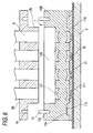
- Fig. 8 is a sectional view illustrating the construction of an optical transmission module according to a sixth embodiment of the invention.
- an optical part includes a guide pin but does not include an optical fiber receptacle section, compared with the fourth embodiment shown in Fig. 6.
- the optical part 13D includes the lens section 131 and the guide pin insertion hole 133, but does not include an optical fiber receptacle section. However, the optical fiber can be fixed to the optical part 13D using the guide pin 15.
- the photoelectric elements 12 and the optical part 13D are directly positioned with respect to the mounting support member 11A, and the optical section 13D and the optical fiber 4 are positioned by the guide pin 15. Therefore, without an intermediate member, positioning with high precision can be realized. Further, the optical part 13D does not need to be provided with an optical fiber receptacle member, which makes it easy to manufacture the optical part 13D.
- An optical transmission module has a mirror surface provided in an optical part.
- the mirror surface reflects an optical signal emitted from a photoelectric element in a direction parallel to the substrate surface.
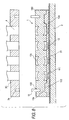
- Figs. 9A and 9B are sectional views illustrating the structure of the optical transmission module according, to the seventh embodiment of the invention.
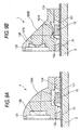
- Fig. 9A shows the optical transmission module using only the mirror surface without a lens section
- Fig. 9B shows the optical transmission module using the lens section and the mirror surface.
- the optical part 13E shown in Fig. 9A has a concave portion (not shown) where a convex portion of the optical part positioning section 112 provided in the mounting support member 11A is fitted, similar to other embodiments. Further the optical part 13E has a mirror surface 135A which bends an optical signal, which is diffusely emitted from the photoelectric element 12, in a direction parallel to the substrate 2 and condenses light.
- Fig. 9A the optical signal emitted from the photoelectric element 12 proceeds while being diffused upward. If the optical signal proceeds into the optical part 13E, the diffusion width thereof is suppressed in a relationship of a refractive index.
- the optical signal When the optical signal further proceeds so as to approach the mirror surface 135A, the optical signal is reflected in the horizontal direction. At this time, since the surface mirror 135A is a concave surface mirror, the optical signal which was being diffused proceeds while being converged.
- the optical signal proceeds outside the optical part 13E, the optical signal approaches the optical fiber receptacle section 132 while being further converged due to a change in refractive index. Then, the optical signal is incident on the optical fiber held by a fiber holder (not shown) which is fitted into the optical fiber receptacle section 132.
- the optical part 13F shown in Fig. 9B has a concave portion (not shown) which is fitted into the convex portion of the optical part positioning section 112 provided in the mounting support member 11A, similar to other embodiments. Further, the optical part 13F includes a lens section 131A which changes an optical signal, diffusely emitted from the photoelectric element 12, into parallel light; a mirror surface 135B which bends the parallel light in a direction parallel to the substrate 2; and a lens section 131B which condenses the parallel light reflected by the mirror surface 135B.
- the optical signal emitted from the photoelectric element 12 proceeds while being diffused upward.
- the optical signal approaches the optical part 13F, the optical signal is refracted by the lens section 131A so as to become parallel light.
- the parallel light proceeds within the optical part 13F.
- the parallel light approaches the mirror surface 135B and is reflected in the horizontal direction. At this time, since the mirror surface 135B is a plane surface mirror, the parallel light is maintained as it is.
- the optical signal proceeds outside the optical part 13E, the optical signal is once again refracted by the lens section 131B and then approaches the optical fiber receptacle section 132 while being converged. Then, the optical signal is incident on the optical fiber held by a fiber holder (not shown) which is fitted into the optical fiber receptacle section 132.
- the photoelectric element 12 and the optical part 13E or 13F are directly positioned with respect to the mounting support member 11A, similar to the first embodiment. Therefore, without an intermediate member such as a guide pin, positioning with high precision can be realized. At the same time, the optical signal can be caused to proceed in the horizontal direction, without increasing the number of parts.
- the optical part is provided with the optical fiber receptacle section and the lens section.
- the optical part may be provided with only one of the optical fiber receptacle section and the lens section.
Landscapes
- Physics & Mathematics (AREA)
- General Physics & Mathematics (AREA)
- Optics & Photonics (AREA)
- Optical Couplings Of Light Guides (AREA)
Abstract
Description
- The present invention relates to an optical transmission module and a method of manufacturing the same, particularly an optical transmission module in which positioning between a photoelectric element and an optical fiber can be achieved precisely and easily, and reduction in size and cost can be realized.
- A conventional optical transmission module is provided with a plurality of photoelectric elements such as light emitting elements or light receiving elements. In the optical transmission module, positioning of the photoelectric element and an optical fiber has been a serious problem.
- When one photoelectric element is provided, the photoelectric element is housed in a metallic can package such as a TO (Transistor Outline) can package, and a so-called active alignment is performed in which positioning between the photoelectric element and an optical fiber receptacle section is performed in a state where the photoelectric element emits light or receives light.
- In such a method, however, photoelectric elements should be positioned one-by-one during operation. Therefore, a cost becomes high. As a method for improving such a problem, a method has been proposed in which an optical change section such as a lens changing an optical path is provided in a package sealing a light receiving and emitting element through resin molding (for example, refer to
JP-A-11-133274 - In an optical transmission module having a plurality of photoelectric elements, a problem of positioning becomes more important. In an array-shaped optical transmission module in which photoelectric elements are monolithically formed in an array shape, a positioning member such as a guide pin is used, so that an optical fiber, an optical receptacle, a photoelectric conversion section, and the photoelectric elements are positioned with respect to the guide pin (for example, refer to
JP-A-2000-199838 - In the method disclosed in Patent Document 1, however, positioning of a mold and a photoelectric part is limited, and a deviation of dimension is generated in accordance with a change in temperature when molding is performed. Therefore, the precision of positioning is limited, and the method cannot be used in a small-diameter fiber, which is used in high-speed transmission.
- In the method disclosed in
Patent Document 2, the respective parts are precisely positioned with respect to the guide pin. Therefore, each part needs to have a hole formed with high precision and at a certain depth, the hole passing through the guide pin. Accordingly, a manufacturing cost of each part becomes high. Further, the thickness of each part and a housing section of the pin are provided, thereby preventing miniaturization of the module. - In the optical transmission module in which a plurality of photoelectric elements are separately disposed, the problem of positioning is further serious, and a suitable solution has not been provided.
- An object of the present invention is that it provides an optical transmission module and a method of manufacturing the same. In the optical transmission module, positioning between a photoelectric element and an optical fiber can be achieved precisely and easily, and reduction in size and cost can be realized.
- In order to achieve the object, one embodiment of the invention provides the following optical transmission module and the method of manufacturing the same.
- (1) According to an aspect of the present invention, an optical transmission module comprising: a substrate; an electric wiring section that is provided on the substrate; a photoelectric element that are mounted on the electric wiring section, and that emits an optical signal on the basis of a received electric signal or transmits an electric signal on the basis of a received optical signal; an optical part that comprises at least one of an optical conversion section and an optical fiber receptacle section, and that controls an optical path of optical signal between the photoelectric element and an optical fiber; a mounting support member that positions the photoelectric element; and a positioning mechanism that positions the optical part and the mounting support member.
In accordance with this aspect, the photoelectric element is positioned by the mounting support member, and the mounting support member and the optical part are positioned by the positioning mechanism. Accordingly, the photoelectric element and the optical part can be positioned precisely and easily through the mounting support member. - (2) The optical transmission module as described in the item (1), wherein the photoelectric element and the mounting support member are mounted on an upper surface of the electric wiring section, and the optical part is mounted on the mounting support member.
In accordance with this aspect, since the photoelectric element and the mounting support member are mounted on the upper surface of the electric wiring section, that is, on the same surface, mounting precision becomes high. - (3) The optical transmission module as described in the item (1), wherein the photoelectric element emitting the optical signal is a surface emitting laser.
In accordance with this aspect, a combination with VCSEL, which is expected to be a low-cost light emitting element, have the largest effect, and positioning can be performed at a low cost. - (4) The optical transmission module as described in the item (1), wherein the positioning mechanism comprises: one of a first convex portion and a first concave portion that is provided in the mounting support member; and one of a second concave portion and a second convex portion that is fitted into the one of the first convex portion and the second concave portion, and that is provided in the optical part.
In accordance with this aspect, the first and second convex portion and the first and second concave portion, which are fitted to each other, are used as the positioning mechanism, which makes it possible to perform positioning at a low cost. - (5) The optical transmission module as described in the item (4), wherein the positioning mechanism is provided with a plurality of the one of the first convex portions and the first concave portions and a plurality of the second concave portions and the second convex portions, respectively.
In accordance with this aspect, the pluralities of the first and second convex portions and the first and second concave portions, which are fitted to each other, are used, so that positioning with high precision can be achieved. - (6) The optical transmission module as described in the item (1), wherein the mounting support member is a resin molding product.
In accordance with this aspect, a resin molding product is used as the mounting support member. Therefore, even though the optical product has a complex shape, mass productivity is high, and a low cost can be achieved. - (7) The optical transmission module as described in the item (1), wherein the optical part is a resin molding product.
In accordance with this aspect, a resin molding product is used as the optical part. Therefore, even though the optical product has a complex shape, mass productivity is high, and a low cost can be achieved. - (8) The optical transmission module as described in the item (1), wherein a plurality of the photoelectric elements are provided; and the optical receptacle section fixing the plurality of optical fibers.
In accordance with this aspect, the plurality of optical fibers can be fixed, thereby achieving the miniaturization. - (9) The optical transmission module as described in the item (6), wherein the plurality of photoelectric element are an integral array product.
In accordance with this aspect, it is possible to achieve the miniaturization. - (10) The optical transmission module as described in the item (9), wherein the mounting support member individually positions on the plurality of photoelectric elements.
- (11) The optical transmission module as described in any one of the items (1), (9) and (10), wherein the mounting support member comprises an element positioning section containing a hole positioning the photoelectric element.
In accordance with this aspect, since the photoelectric element can be mechanically positioned, the positioning of the photoelectric element becomes easy. - (12) The optical transmission module as described in the item (11), wherein the positioning of the photoelectric element with respect to the mounting support member is mechanically performed by fitting a wall surface of the photoelectric element to a wall surface of the element positioning section.
According to this aspect, since the photoelectric element can be mechanically positioned, the positioning of the photoelectric element becomes easy. - (13) The optical transmission module as described in the item (12), wherein the wall surface of the element positioning section comprises an inclined surface.
In accordance with this aspect, mechanical interference hardly occurs. Such a structure makes mounting easy. - (14) The optical transmission module as described in the item (11), wherein the mounting support member comprises a plurality of alignment marks positioning the photoelectric element.
In accordance with this aspect, the positioning of the photoelectric element can be optically performed by using the alignment marks, so that high positioning precision of the photoelectric element is obtained. - (15) The optical transmission module as described in the item (1), wherein the mounting support member comprises an element positioning section containing a hole positioning the photoelectric element.
In accordance with this aspect, the convex of concave portion is used for fixing the fiber holder, so that positioning can be easily performed at a low cost. - (16) A method of manufacturing an optical transmission module comprising: installing a mounting support member on a substrate such that the disposed position of photoelectric element on the substrate with respect to an electric wiring section coincides with an element positioning section provided in the mounting support member; installing the photoelectric element on the substrate in accordance with the element positioning section; connecting the photoelectric element to the electric wiring section by using wire; and installing an optical part in accordance with an optical part positioning section provided in the mounting support member.
In accordance with this aspect, the photoelectric element is positioned by the element positioning section of the mounting support member, and the optical part is positioned by the optical part positioning section provided in the mounting support member. Accordingly, the photoelectric element and the optical part can be easily positioned through the mounting support member. - (17) The method of manufacturing an optical transmission module as described in the item (16), which comprises: sealing the periphery of the photoelectric element after the installing of the optical part.
- According to the present invention, it is possible to provide the optical transmission module and the method of manufacturing the same, in which the positioning of the photoelectric element and the optical fiber can be realized precisely and easily, and the miniaturization and cost reduction can be achieved.
- Exemplary embodiment of the present invention will be described in detail based on the following figures, wherein:
- Fig. 1 is a sectional view illustrating the construction of an optical transmission module according to a first embodiment of the present invention;
- Figs. 2A and 2B are diagrams illustrating the structure of a mounting support member according to a first embodiment of the invention;
- Figs. 3A to 3F are diagrams illustrating a process of manufacturing an optical transmission module according to the first embodiment of the invention;
- Figs. 4A and 4B are diagrams illustrating the structure of a mounting support member according to a second embodiment of the invention;
- Figs. 5A and 5B are diagrams illustrating the structure of a mounting support member according to a third embodiment of the invention;
- Fig. 6 is a sectional view illustrating the structure of an optical transmission module according to a fourth embodiment of the invention;
- Fig. 7 is a sectional view illustrating the structure of an optical transmission module according to a fifth embodiment of the invention;
- Fig. 8 is a sectional view illustrating the structure of an optical transmission module according to a sixth embodiment of the invention; and
- Figs. 9A and 9B are sectional views illustrating the structure of an optical transmission module according to a seventh embodiment of the invention.
- Fig. 1 is a sectional view illustrating the construction of an optical transmission module according to a first embodiment of the invention.
- The optical transmission module 1 includes a mounting
support member 11A, a plurality ofphotoelectric elements 12, and anoptical part 13A. The mountingsupport member 11A is provided on anelectric wiring section 21 disposed on asubstrate 2. - The
electric wiring section 21 is an electric wiring part such as a printed circuit board, a flexible printed circuit board, a lead frame wiring lines or the like. Theelectric wiring section 21 is disposed on thesubstrate 2 in advance. - The mounting
support member 11A makes it possible to dispose thephotoelectric element 12 in an optimal position on theelectric wiring section 21 and to install theoptical part 13A in an optimal position in the positional relationship with thephotoelectric element 12. - The mounting
support member 11A is provided with a plurality ofelement positioning sections 111 and a plurality of opticalpart positioning sections 112. Theelement positioning section 111 is used in positioning for disposing thephotoelectric element 12 on an optimal position of theelectric wiring section 21, in order to connect thephotoelectric element 12 to theelectric wiring section 21. - The optical
part positioning section 112 is a convex portion (first convex portion) provided on the upper surface of the mountingsupport member 11A. The opticalpart positioning section 112 is fitted into a concave portion (second concave portion) 13a provided in theoptical part 13A, so that theoptical part 13A can be fixed in a suitable position. - The
photoelectric element 12 is a light emitting element such as a light emitting diode or surface emitting laser, which converts an electric signal into an optical signal. When receiving an electric signal delivered through theelectric wiring section 21, thephotoelectric element 12 emits a corresponding optical signal to deliver to optical fiber (not shown) through theoptical part 13A. Alternatively, thephotoelectric element 12 may be a light receiving element, such as a photodiode, which receives an optical signal emitted from the optical fiber (not shown) through theoptical part 13A and converts the optical signal into an electrical signal to return. Further, as for the plurality ofphotoelectric elements 12 on thesubstrate 2, light emitting elements and light receiving elements may be used. - As for the
photoelectric element 12, a light emitting element, such as surface emitting laser, or a light receiving element is used. However, any element, which performs photoelectric conversion, may be used. - The
optical part 13A includes a plurality oflens sections 131 and an opticalfiber receptacle section 132. Theoptical part 13A has a function of effectively delivering an optical signal emitted from thephotoelectric element 12 to the optical fiber 4. - The
lens section 131 condenses optical signals, which are diffusely emitted from thephotoelectric element 12, and performs photoelectric conversion so that the optical signals effectively enter the optical fiber. Alternatively, when a light receiving element is used as thephotoelectric element 12, the lens section condenses optical signals, which are diffusely emitted from the optical fiber, and performs photoelectric conversion so that the optical signals are effectively condensed and received into thephotoelectric element 12. - The optical
fiber receptacle section 132 fits and fixes one end of afiber holder 3A holding the optical fiber 4 delivering an optical signal to an optimal position so that an optical signal emitted from thephotoelectric element 12 is effectively received and an optical signal received in thephotoelectric element 12 is effectively transmitted. - Figs. 2A and 2B are diagrams illustrating the detailed structure of the mounting support member according to the first embodiment. Fig. 2A is a top view of the mounting
support member 11A and Fig. 2B is a sectional view taken along an A-A line of Fig. 2A. - The mounting
support member 11A is a thin plate member having a substantially rectangular shape. The opticalpart positioning section 112 having a convex shape is provided on either side of the mountingsupport member 11A in a longitudinal direction. Between two of the opticalpart positioning sections 112, the plurality (four in Fig. 2) ofelement positioning sections 111 are provided, having a width for positioning a width direction of thephotoelectric element 12. - The
element positioning section 111 is a hole provided through the plane-shaped mountingsupport member 11A. When the mountingsupport member 11A is disposed on theelectric wiring section 21, theelectric wiring section 21 is exposed through theelement positioning section 111 without being covered by the mountingsupport member 11A. Therefore, when thephotoelectric element 12 is disposed in theelement positioning section 111, the electric connection between thephotoelectric element 12 and theelectric wiring section 21 can be achieved. - The wall surface of the
element positioning section 111 is formed with aninclined surface 111a. Therefore, when thephotoelectric element 12 is mounted, mechanical interference hardly occurs. Such a structure makes mounting easy. - A
taper 112a is formed at the side of the opticalpart positioning section 112 so that theoptical part 13A is easily fitted. - Figs. 3A to 3F are diagrams illustrating a process of manufacturing an optical transmission module according to the first embodiment of the invention. Figs. 3B, 3D, and 3F are sectional views taken along an A-A line of Figs. 3A, 3C, and 3E, respectively.
- First, the
electric wiring section 21 is disposed on thesubstrate 2. Then, the mountingsupport member 11A is positioned and fixed in accordance with an electrode pattern of theelectric wiring section 21 and other positional information, as shown in Figs. 3A and 3B. - The
electric wiring section 21 is directly disposed on thesubstrate 2, for example, by a method of printing a circuit board on thesubstrate 2. - The mounting
support member 11A can be formed in a desired shape by resin molding, such as extrusion, or a cutting. - The mounting
support member 11A is used for determining an absolute position of thephotoelectric element 12 with respect to theelectric wiring section 21. However, an absolute position of thephotoelectric element 12 with respect to theelectric wiring section 21 has a relatively high degree of freedom. Therefore, the mounting precision of the mountingsupport member 11A with respect to theelectric wiring section 21 may be relatively low, and mounting can be performed at a low cost. - Next, as shown in Figs. 3B and 3E, the plurality of
photoelectric elements 12 are disposed using theelement positioning section 111 of the mountingsupport member 11A and fixed to theelectric wiring section 21. - The width of one side of the
element positioning section 111 composed of a substantially rectangular hole slightly exceeds that of thephotoelectric element 12. Further, thephotoelectric element 12 is disposed in accordance with the element positioning section of the mountingsupport member 11A, so that thephotoelectric element 12 can be easily disposed in a desired position. - The width of the other side of the
element positioning section 111 is relatively larger than that ofphotoelectric element 12. This is because a space required for connecting an electrode provided on thephotoelectric element 12 and theelectric wiring section 21 through wire-bonding using wire 12a should be secured. - After the fixing of the
photoelectric element 12, the electrode provided on thephotoelectric element 12 and theelectric wiring section 21 are connected through wire-bonding using thewire 12a. Since heat is generated in the wire-bonding, the mountingsupport member 11A is preferably formed of a material having resistance to the heat. - The wall surface of the
element positioning section 111 is inclined, so that the size of the hole at the upper portion becomes larger than that of the hole at the lower portion, which makes it easy to dispose thephotoelectric element 12. - Next, as shown in Figs. 3C and 3F, the
optical part 13A is disposed on the mountingsupport member 11A. At this time, the disposed position of theoptical part 13A is determined using two of the opticalpart positioning sections 112 of the mountingsupport member 11A. As the convex-shaped opticalpart positioning section 112 of the mounting support member 11 is fitted into theconcave portion 13a of theoptical part 13A, the plurality oflens sections 131 of the optical part 13 are respectively positioned on the correspondingphotoelectric elements 12. That is, the plurality oflens sections 131 can be disposed in suitable positions. - The optical
part positioning section 112 is provided with thetaper 112a so that theoptical part 13A is easily fitted into the opticalpart positioning section 112. Therefore, when theoptical part 13A is positioned with respect to the mountingsupport member 11A, mechanical interference hardly occurs. Such a structure makes mounting easy. - The
optical part 13A can be also formed in a desired shape by resin molding, such as extrusion, or a cutting. - The above-described process of manufacturing the optical transmission module according to the first embodiment is commonly applied to optical transmission modules according to other embodiments, which will be described below.
- According to the first embodiment, the
photoelectric element 12 and theoptical part 13A are directly positioned with respect to the mountingsupport member 11A. Therefore, without an intermediate member such as a guide pin, positioning with high precision can be realized. Further, since the thickness of the mountingsupport member 11A can be set to the thickness level of thephotoelectric element 12, the mounting support member can be manufactured at a low cost. - Further, even in the
optical fiber receptacle 132, positioning of the optical fiber can be realized without an intermediate member such as a guide pin. - An optical transmission module according to a second embodiment of the invention has alignment marks provided in a mounting support member, and the alignment marks are used for determining the disposed position of the
photoelectric element 12. - Figs. 4A and 4B are diagrams illustrating the structure of the mounting support member according to the second embodiment of the invention. Fig. 4A is a top view of the mounting
support member 11B, and Fig. 4B is a sectional view taken along a line A-A of Fig. 4A. - The mounting
support member 11B according to the second embodiment has something in common with the mountingsupport member 11A according to the first embodiment in that the mountingsupport member 11B is a slim plate member having a substantially rectangular shape, the convex-shaped opticalpart positioning section 112 is provided on either side of the mountingsupport member 11B in the longitudinal direction, and the plurality ofelement positioning sections 111 are provided between two of the opticalpart positioning sections 112. However, the mountingsupport member 11B is different from the mountingsupport member 11A in that the alignment marks 113 are provided around eachelement positioning section 111. - The alignment marks 113 are provided around the plurality of
element positioning sections 111 of the mountingsupport member 11B. The alignment mark is a straight-line mark provided around theelement positioning section 111 and is a concave portion, which is provided in advance when the mountingsupport member 11B is molded. - The plurality of alignment marks 113 are provided around each of the
element positioning sections 111. Optical positioning is performed such that a point, where the respective alignment marks 113 intersect each other when they are extended, overlaps the center of theoptical element 12. Then, the absolute position of theoptical element 12 is determined. - Therefore, the width of the
element positioning section 111 in the mountingsupport member 11B may be relatively larger than that of theoptical element 12. Further, the wall surface of theelement positioning section 111 does not have to be formed with theinclined surface 111a. - When the
photoelectric element 12 is positioned, mechanical positioning using theelement positioning section 111 and optical positioning using the alignment marks 113 may be used together. - According to the second embodiment, the
photoelectric element 12 and theoptical part 13A are directly positioned with respect to the mountingsupport member 11B. Therefore, without an intermediate member such as a guide pin, positioning with high precision can be realized. - An optical transmission module according to a third embodiment of the invention has one array positioning section provided in a mounting support member. The disposed position of an element array including a plurality of photoelectric elements is determined by the array positioning section.
- Figs. 5A and 5B are diagrams illustrating the structure of the mounting support member according to the third embodiment of the invention. Fig. 5A is a top view of the mounting
support member 11C, and the Fig. 5B is a sectional view taken along a line A-A of Fig. 5A. Figs. 5A and 5B shows theelement array 14 disposed inside thearray positioning section 114. - In the mounting
support member 11C, onearray positioning section 114 and a plurality (for example, two) of opticalpart positioning sections 112 are provided. Thearray positioning section 114 is used in positioning for disposing theelement array 14 on an optimal position of theelectric wiring section 21, in order to connect theelement array 14 including the plurality of photoelectric elements to theelectric wiring section 21. - The
element array 14 is where a plurality of photoelectric elements converting an electric signal into an optical signal are arranged. When the respective photoelectric elements receive an electric signal delivered through theelectric wiring section 21, theelement array 14 emits a corresponding optical signal to deliver to the optical fiber 4 (not shown) through theoptical part 13A. When a light receiving element is used as a photoelectric element, the respective photoelectric elements receive an optical signal emitted from the optical fiber 4 (not shown) through theoptical part 13A and return the optical signal into an electric signal. - As for the photoelectric element included in the
element array 14, a light emitting element such as surface emitting laser or a light receiving element is used. However, any element which performs photoelectric conversion may be used. - The mounting
support member 11C is a slim plate member having a substantially rectangular shape. The convex-shaped opticalpart positioning section 112 is provided on either side of the mountingsupport member 11C in a longitudinal direction. Further, between two of the opticalpart positioning sections 112, one rectangulararray positioning section 114 is provided. - The
array positioning section 114 is a hole provided in the plane mountingsupport member 11C. When the mountingsupport member 11C is disposed on theelectric wiring section 21, theelectric wiring section 21 is exposed through thearray positioning section 114 without being covered by the mountingsupport member 11C. Therefore, when theelement array 14 is disposed in thearray positioning section 114, the electric connection between theelement array 14 and theelectric wiring section 21 can be achieved. - The wall surface of the
array positioning section 114 is formed with aninclined surface 114a. When theelement array 114 is mounted, mechanical interference hardly occurs. Therefore, such a structure makes mounting easy. - In the above-described third embodiment, alignment marks are not used in positioning the
element array 14. However, alignment marks may be used for positioning theelement array 14. - According to the third embodiment, the
element array 14 and theoptical part 13A are directly positioned with respect to the mountingsupport member 11C. Therefore, without an intermediate member such as a guide pin, positioning with high precision can be realized. - An optical transmission module according to the fourth embodiment of the invention has a plurality of guide pins provided in the side of an optical fiber receptacle provided in an optical part. The guide pin is used for the connection between the optical part and the optical fiber.
- Fig. 6 is a sectional view illustrating the structure of the optical transmission module according to the fourth embodiment of the invention.
- The optical transmission module 1 according to the fourth embodiment includes a mounting
support member 11A, a plurality ofphotoelectric elements 12, theoptical part 13B, and the plurality of guide pins 15. The mountingsupport member 11A is provided on theelectric wiring section 21 disposed on thesubstrate 2. The mountingsupport member 11A and thephotoelectric elements 12 are the same as those of the first embodiment. - The
optical part 13B includes a plurality oflens sections 131, the opticalfiber receptacle section 132, and a plurality of guide pin insertion holes (third concave portions) 133. Theoptical part 13B has a function of effectively delivering an optical signal emitted from thephotoelectric element 12 to the optical fiber. - The
lens section 131 and the opticalfiber receptacle section 132 are the same as those of theoptical part 13A according to the first embodiment and have the same function. - The guide
pin insertion hole 133 is provided at the upper surface of theoptical part 13B and at the side of the opticalfiber receptacle section 132. Theguide pin 15 is inserted into the guidepin insertion hole 133. - After being inserted into the guide
pin insertion hole 133, theguide pin 15 is used for connecting the optical fiber 4 (not shown) to the opticalfiber receptacle section 132. In this case, afitting section 3b of thefiber holder 3B holding the plurality of optical fibers 4 is fitted into theoptical fiber receptacle 132, and theguide pin 15 is inserted into apin hole 3a. When theguide pin 15 is inserted into a guide positioned at the side of the receptacle provided at one end of the optical fiber, thefitting section 3b is loosely fitted into the opticalfiber receptacle section 132 and is positioned by theguide pin 15. Therefore, the optical fiber 4 is easily inserted into the opticalfiber receptacle section 132, and the optical fiber 4 can be stably fixed. - According to the fourth embodiment, the
photoelectric elements 12 and theoptical part 13B are directly positioned with respect to the mountingsupport member 11A, and the optical fiber 4 is positioned by theguide pin 15. Therefore, positioning with high precision can be realized. - Fig. 7 is a sectional view illustrating the construction of an optical transmission module according to a fifth embodiment of the invention. Although the
guide pin 15 is inserted into the guidepin insertion hole 133 provided in theoptical part 13B in the fourth embodiment, theoptical part 13B and theguide pin 15 are integrally formed in this embodiment. - The
optical part 13C composing the optical transmission module 1 shown in Fig. 7 has aguide pin 134 provided in the side of an opticalfiber receptacle section 132. Theguide pin 134 is formed of the same material as theoptical part 13C. Theguide pin 134 is provided in advance when theoptical part 13C is formed. That is, theguide pin 134 and theoptical part 13C are integrally formed. - The
guide pin 134 has the same function as theguide pin 15 shown in Fig. 6. Theguide pin 134 is different from theguide pin 15 only in that theguide pin 134 and the optical part are integrally formed. - When the guide pin is used for fixing the optical fiber to the optical part, the optical fiber receptacle section may be omitted.
- According to the fifth embodiment, the
photoelectric element 12 and theoptical part 13C are directly positioned with respect to the mountingsupport member 11A, and theoptical part 13C and the optical fiber 4 are positioned by theguide pin 134. Therefore, positioning with high precision can be realized. Further, theguide pin 134 and theoptical part 13C are integrally formed, which makes it easy to manufacture the optical part. - Fig. 8 is a sectional view illustrating the construction of an optical transmission module according to a sixth embodiment of the invention. In this embodiment, an optical part includes a guide pin but does not include an optical fiber receptacle section, compared with the fourth embodiment shown in Fig. 6.
- The
optical part 13D includes thelens section 131 and the guidepin insertion hole 133, but does not include an optical fiber receptacle section. However, the optical fiber can be fixed to theoptical part 13D using theguide pin 15. - According to the sixth embodiment, the
photoelectric elements 12 and theoptical part 13D are directly positioned with respect to the mountingsupport member 11A, and theoptical section 13D and the optical fiber 4 are positioned by theguide pin 15. Therefore, without an intermediate member, positioning with high precision can be realized. Further, theoptical part 13D does not need to be provided with an optical fiber receptacle member, which makes it easy to manufacture theoptical part 13D. - An optical transmission module according to a seventh embodiment of the invention has a mirror surface provided in an optical part. The mirror surface reflects an optical signal emitted from a photoelectric element in a direction parallel to the substrate surface.
- Figs. 9A and 9B are sectional views illustrating the structure of the optical transmission module according, to the seventh embodiment of the invention. Fig. 9A shows the optical transmission module using only the mirror surface without a lens section, and Fig. 9B shows the optical transmission module using the lens section and the mirror surface.
- The
optical part 13E shown in Fig. 9A has a concave portion (not shown) where a convex portion of the opticalpart positioning section 112 provided in the mountingsupport member 11A is fitted, similar to other embodiments. Further theoptical part 13E has amirror surface 135A which bends an optical signal, which is diffusely emitted from thephotoelectric element 12, in a direction parallel to thesubstrate 2 and condenses light. - In Fig. 9A, the optical signal emitted from the
photoelectric element 12 proceeds while being diffused upward. If the optical signal proceeds into theoptical part 13E, the diffusion width thereof is suppressed in a relationship of a refractive index. - When the optical signal further proceeds so as to approach the
mirror surface 135A, the optical signal is reflected in the horizontal direction. At this time, since thesurface mirror 135A is a concave surface mirror, the optical signal which was being diffused proceeds while being converged. - When the optical signal proceeds outside the
optical part 13E, the optical signal approaches the opticalfiber receptacle section 132 while being further converged due to a change in refractive index. Then, the optical signal is incident on the optical fiber held by a fiber holder (not shown) which is fitted into the opticalfiber receptacle section 132. - The
optical part 13F shown in Fig. 9B has a concave portion (not shown) which is fitted into the convex portion of the opticalpart positioning section 112 provided in the mountingsupport member 11A, similar to other embodiments. Further, theoptical part 13F includes alens section 131A which changes an optical signal, diffusely emitted from thephotoelectric element 12, into parallel light; amirror surface 135B which bends the parallel light in a direction parallel to thesubstrate 2; and alens section 131B which condenses the parallel light reflected by themirror surface 135B. - In Fig. 9B, the optical signal emitted from the
photoelectric element 12 proceeds while being diffused upward. When the optical signal approaches theoptical part 13F, the optical signal is refracted by thelens section 131A so as to become parallel light. The parallel light proceeds within theoptical part 13F. - If the parallel light further proceeds, the parallel light approaches the
mirror surface 135B and is reflected in the horizontal direction. At this time, since themirror surface 135B is a plane surface mirror, the parallel light is maintained as it is. - Further, when the optical signal proceeds outside the
optical part 13E, the optical signal is once again refracted by thelens section 131B and then approaches the opticalfiber receptacle section 132 while being converged. Then, the optical signal is incident on the optical fiber held by a fiber holder (not shown) which is fitted into the opticalfiber receptacle section 132. - According to the seventh embodiment, the
photoelectric element 12 and theoptical part support member 11A, similar to the first embodiment. Therefore, without an intermediate member such as a guide pin, positioning with high precision can be realized. At the same time, the optical signal can be caused to proceed in the horizontal direction, without increasing the number of parts. - The present invention is not limited to the above-described embodiments, but modifications can be made without departing from the scope of the invention. Further, the components of the respective embodiments can be arbitrarily combined without departing from the scope of the invention.
- In the above-described embodiments, the optical part is provided with the optical fiber receptacle section and the lens section. However, the optical part may be provided with only one of the optical fiber receptacle section and the lens section.
Claims (17)
- An optical transmission module comprising:a substrate;an electric wiring section that is provided on the substrate;a photoelectric element that are mounted on the electric wiring section, and that emits an optical signal on the basis of a received electric signal or transmits an electric signal on the basis of a received optical signal;an optical part that comprises at least one of an optical conversion section and an optical fiber receptacle section, and that controls an optical path of optical signal between the photoelectric element and an optical fiber;a mounting support member that positions the photoelectric element; anda positioning mechanism that positions the optical part and the mounting support member.
- The optical transmission module according to claim 1, wherein
the photoelectric element and the mounting support member are mounted on an upper surface of the electric wiring section, and
the optical part is mounted on the mounting support member. - The optical transmission module according to claim 1, wherein the photoelectric element emitting the optical signal is a surface emitting laser.
- The optical transmission module according to claim 1, wherein
the positioning mechanism comprises:one of a first convex portion and a first concave portion that is provided in the mounting support member; andone of a second concave portion and a second convex portion that is fitted into the one of the first convex portion and the second concave portion, and that is provided in the optical part. - The optical transmission module according to claim 4, wherein
the positioning mechanism is provided with a plurality of the one of the first convex portions and the first concave portions and a plurality of the second concave portions and the second convex portions, respectively. - The optical transmission module according to claim 1, wherein the mounting support member is a resin molding product.
- The optical transmission module according to claim 1, wherein the optical part is a resin molding product.
- The optical transmission module according to claim 1, wherein
a plurality of the photoelectric elements are provided; and
the optical receptacle section fixing the plurality of optical fibers. - The optical transmission module according to claim 6, wherein the plurality of photoelectric element are an integral array product.
- The optical transmission module according to claim 9, wherein the mounting support member individually positions on the plurality of photoelectric elements.
- The optical transmission module according to any one of claims 1, 9 and 10, wherein the mounting support member comprises an element positioning section containing a hole positioning the photoelectric element.
- The optical transmission module according to claim 11,
wherein
the positioning of the photoelectric element with respect to the mounting support member is mechanically performed by fitting a wall surface of the photoelectric element to a wall surface of the element positioning section. - The optical transmission module according to claim 12, wherein the wall surface of the element positioning section comprises an inclined surface.
- The optical transmission module according to claim 11, wherein the mounting support member comprises a plurality of alignment marks positioning the photoelectric element.
- The optical transmission module according to claim 1,
wherein the optical part is one of a third convex portion and a third concave portion fixing a fiber holder holding the plurality of optical fibers. - A method of manufacturing an optical transmission module comprising:installing a mounting support member on a substrate such that the disposed position of photoelectric element on the substrate with respect to an electric wiring section coincides with an element positioning section provided in the mounting support member;installing the photoelectric element on the substrate in accordance with the element positioning section;connecting the photoelectric element to the electric wiring section by using wire; andinstalling an optical part in accordance with an optical part positioning section provided in the mounting support member.
- The method of manufacturing an optical transmission module according to claim 16, which comprises:sealing the periphery of the photoelectric element after the installing of the optical part.
Applications Claiming Priority (1)
| Application Number | Priority Date | Filing Date | Title |
|---|---|---|---|
| JP2006137955A JP2007310083A (en) | 2006-05-17 | 2006-05-17 | Optical transmission module and method for manufacturing the same |
Publications (1)
| Publication Number | Publication Date |
|---|---|
| EP1857849A1 true EP1857849A1 (en) | 2007-11-21 |
Family
ID=38512610
Family Applications (1)
| Application Number | Title | Priority Date | Filing Date |
|---|---|---|---|
| EP06023372A Withdrawn EP1857849A1 (en) | 2006-05-17 | 2006-11-09 | Optical transmission module and method of manufacturing the same |
Country Status (5)
| Country | Link |
|---|---|
| US (1) | US7449674B2 (en) |
| EP (1) | EP1857849A1 (en) |
| JP (1) | JP2007310083A (en) |
| KR (1) | KR100844068B1 (en) |
| CN (1) | CN101075007B (en) |
Cited By (1)
| Publication number | Priority date | Publication date | Assignee | Title |
|---|---|---|---|---|
| WO2013134449A1 (en) * | 2012-03-08 | 2013-09-12 | Tyco Electronics Corporation | Molded optical component with inspection features and method fpr tuning a mold |
Families Citing this family (46)
| Publication number | Priority date | Publication date | Assignee | Title |
|---|---|---|---|---|
| JP4983703B2 (en) * | 2008-04-08 | 2012-07-25 | 日立電線株式会社 | Optical transmission system |
| US20100252856A1 (en) * | 2009-01-28 | 2010-10-07 | Coretek Opto Corp. | Header structure of opto-electronic element and opto-electronic element using the same |
| US8090230B1 (en) * | 2009-02-12 | 2012-01-03 | Compass Electro-Optical Systems | Method and device for light coupling |
| JP5302714B2 (en) * | 2009-02-26 | 2013-10-02 | 富士通コンポーネント株式会社 | Optical connector |
| US8351794B2 (en) * | 2009-03-10 | 2013-01-08 | Avago Technologies Fiber Ip (Singapore) Pte. Ltd. | Parallel optical transceiver module having a heat dissipation system that dissipates heat and protects components of the module from particulates and handling |
| JP5328532B2 (en) * | 2009-07-09 | 2013-10-30 | 株式会社フジクラ | Optical connector |
| JP5320190B2 (en) * | 2009-07-09 | 2013-10-23 | 株式会社フジクラ | Optical coupling device |
| JP5158039B2 (en) * | 2009-08-31 | 2013-03-06 | 日立電線株式会社 | Optical transceiver and optical active cable using optical path changing optical block with lens |
| CN102103235B (en) * | 2009-12-18 | 2012-06-27 | 国碁电子(中山)有限公司 | Optical transceiver and manufacturing method thereof |
| WO2011136818A1 (en) * | 2010-04-30 | 2011-11-03 | Hewlett-Packard Development Company, L.P. | Device for converting signal |
| SG185717A1 (en) * | 2010-06-07 | 2012-12-28 | Framatome Connectors Int | Optical circuit board with optical coupling device |
| CN102279446A (en) * | 2010-06-11 | 2011-12-14 | 北京中视中科光电技术有限公司 | Semiconductor laser fiber coupling module |
| JP5543293B2 (en) * | 2010-08-03 | 2014-07-09 | 矢崎総業株式会社 | Small-diameter bending optical connector |
| CN102375185B (en) * | 2010-08-20 | 2013-11-13 | 国碁电子(中山)有限公司 | Optical transceiver and manufacturing method thereof |
| US8834041B2 (en) * | 2011-09-29 | 2014-09-16 | Corning Cable Systems Llc | Ferrule-based optical component assemblies |
| US9170387B2 (en) * | 2011-09-29 | 2015-10-27 | Corning Cable Systems Llc | Optical component assemblies |
| JP2013097004A (en) * | 2011-10-27 | 2013-05-20 | Kyocera Corp | Optical wiring board and optical wiring device |
| WO2013074103A1 (en) * | 2011-11-16 | 2013-05-23 | Intel Corporation | Optical connection techniques and configurations |
| US9435965B2 (en) * | 2012-02-01 | 2016-09-06 | Cisco Technology, Inc. | Single mode fiber array connector for opto-electronic transceivers |
| WO2013158068A1 (en) * | 2012-04-16 | 2013-10-24 | Hewlett-Packard Development Company, L.P. | Integrated optical sub-assembly |
| CN103424818A (en) * | 2012-05-17 | 2013-12-04 | 鸿富锦精密工业(深圳)有限公司 | Photoelectric conversion transmission module |
| US9063313B1 (en) * | 2012-07-06 | 2015-06-23 | Compass Electro Optical System Ltd. | Fiber coupling using collimated beams |
| US20150098680A1 (en) * | 2012-07-27 | 2015-04-09 | Kevin B. Leigh | Optically connecting a chip package to an optical connector |
| JP5737254B2 (en) * | 2012-09-26 | 2015-06-17 | 日立金属株式会社 | Optical communication module |
| GB2506406A (en) * | 2012-09-28 | 2014-04-02 | Ibm | Optical adaptor with horizontal and vertical reference surfaces |
| CN103777286B (en) * | 2012-10-23 | 2017-08-04 | 赛恩倍吉科技顾问(深圳)有限公司 | Photoelectric conversion module |
| TWI560481B (en) * | 2012-10-29 | 2016-12-01 | Hon Hai Prec Ind Co Ltd | Photoelectric converting module |
| JP5621070B1 (en) * | 2012-11-22 | 2014-11-05 | 京セラ株式会社 | Optical connector and optical transmission module |
| CN103869430A (en) * | 2012-12-14 | 2014-06-18 | 鸿富锦精密工业(深圳)有限公司 | Optical fiber connector |
| TWI565989B (en) * | 2012-12-14 | 2017-01-11 | 鴻海精密工業股份有限公司 | Optical fiber connector |
| CN103901557A (en) * | 2012-12-28 | 2014-07-02 | 鸿富锦精密工业(深圳)有限公司 | Photovoltaic conversion module |
| TWI572921B (en) * | 2013-01-25 | 2017-03-01 | 鴻海精密工業股份有限公司 | Optical connector |
| TWI575271B (en) * | 2013-03-06 | 2017-03-21 | 鴻海精密工業股份有限公司 | Optical communication module and glue dispensing method for the optical communication module |
| JP2014182341A (en) * | 2013-03-21 | 2014-09-29 | Hitachi Metals Ltd | Optical connector |
| CN105408793B (en) * | 2013-04-12 | 2018-09-14 | 康宁光电通信有限责任公司 | Optical connections with integral alignment structures |
| CN103257414B (en) * | 2013-05-07 | 2015-08-12 | 苏州旭创科技有限公司 | For the parallel light transceiver component of broadband high-speed transmission |
| CN104422995A (en) * | 2013-08-20 | 2015-03-18 | 鸿富锦精密工业(深圳)有限公司 | Optical-coupling lens and photoelectric conversion module |
| AU2015263909B2 (en) * | 2014-05-23 | 2020-10-08 | Cudoquanta Florida, Inc. | Vision-based passive alignment of an optical fiber subassembly to an optoelectronic device |
| CN103984065B (en) * | 2014-05-30 | 2015-07-15 | 武汉光迅科技股份有限公司 | Optical transmission module |
| US9804349B2 (en) * | 2014-08-13 | 2017-10-31 | Finisar Corporation | Multi-lens optical components |
| WO2018042984A1 (en) * | 2016-08-31 | 2018-03-08 | 住友電気工業株式会社 | Optical connection structure |
| JPWO2020100287A1 (en) * | 2018-11-16 | 2021-02-15 | ナルックス株式会社 | Optical element and positioning method of optical element |
| US10754070B2 (en) * | 2018-12-05 | 2020-08-25 | International Business Machines Corporation | Microlens array assembling process |
| US10690867B1 (en) | 2019-02-12 | 2020-06-23 | International Business Machines Corporation | Optical device with adhesive connection of recess or side protrusion |
| CN110212402B (en) * | 2019-05-07 | 2020-11-27 | 上海灿瑞科技股份有限公司 | Laser diode device |
| EP4481816A4 (en) * | 2022-02-14 | 2025-12-17 | Lipac Co Ltd | OPTICAL SYSTEM IN A BOX, AND OPTICAL MODULE AND OPTICAL TRANSCEIVER USING IT |
Citations (7)
| Publication number | Priority date | Publication date | Assignee | Title |
|---|---|---|---|---|
| EP0121402A2 (en) * | 1983-04-05 | 1984-10-10 | Plessey Overseas Limited | A semiconductor component and method of manufacture |
| WO1998032042A1 (en) * | 1997-01-17 | 1998-07-23 | The Furukawa Electric Co., Ltd. | Optical module |
| US5909524A (en) * | 1996-05-20 | 1999-06-01 | Fujitsu Limited | Optical coupling structure and a fabrication process thereof |
| WO2002054129A1 (en) * | 2000-12-29 | 2002-07-11 | Diemount Gmbh | Coupling device for optically coupling an optical waveguide to an electro-optical element |
| US20040077139A1 (en) * | 2001-01-10 | 2004-04-22 | Kia Silverbrook | Wafer scale fiber optic termination |
| US20040184707A1 (en) | 1999-06-01 | 2004-09-23 | Jewell Jack L. | Opto-mechanical assembly |
| WO2006047896A1 (en) * | 2004-11-03 | 2006-05-11 | Huber+Suhner Ag | Fibre-lens arrangement and lens array for one such fibre-lens arrangement |
Family Cites Families (21)
| Publication number | Priority date | Publication date | Assignee | Title |
|---|---|---|---|---|
| JPS5977402A (en) * | 1982-10-26 | 1984-05-02 | Toshiba Corp | Optical link |
| US5337398A (en) * | 1992-11-30 | 1994-08-09 | At&T Bell Laboratories | Single in-line optical package |
| JPH06237016A (en) * | 1993-02-09 | 1994-08-23 | Matsushita Electric Ind Co Ltd | Optical fiber module and manufacture thereof |
| JP3166564B2 (en) * | 1995-06-27 | 2001-05-14 | 松下電器産業株式会社 | Semiconductor laser package and method of manufacturing the same |
| JPH11133274A (en) | 1997-10-30 | 1999-05-21 | Hitachi Ltd | Optical transmission module |
| KR100300979B1 (en) * | 1998-03-11 | 2001-09-06 | 윤종용 | Module for transmitting light |
| US6328482B1 (en) * | 1998-06-08 | 2001-12-11 | Benjamin Bin Jian | Multilayer optical fiber coupler |
| US6597713B2 (en) * | 1998-07-22 | 2003-07-22 | Canon Kabushiki Kaisha | Apparatus with an optical functional device having a special wiring electrode and method for fabricating the same |
| JP2000199838A (en) | 1999-01-06 | 2000-07-18 | Sumitomo Electric Ind Ltd | Transceiver module for optical parallel transmission |
| FR2807168B1 (en) * | 2000-03-29 | 2002-11-29 | Commissariat Energie Atomique | METHOD AND DEVICE FOR THE PASSIVE ALIGNMENT OF OPTICAL FIBERS AND OPTOELECTRONIC COMPONENTS |
| US6932516B2 (en) * | 2000-07-19 | 2005-08-23 | Canon Kabushiki Kaisha | Surface optical device apparatus, method of fabricating the same, and apparatus using the same |
| JP2002202440A (en) | 2000-12-28 | 2002-07-19 | Japan Aviation Electronics Industry Ltd | Optical module mounting structure and mounting method |
| GB2373064A (en) * | 2001-03-10 | 2002-09-11 | Mitel Corp | Optical fibre connector using transparent filler material |
| US6729771B2 (en) * | 2001-12-17 | 2004-05-04 | Stratos Lightwave, Inc. | Parallel optics subassembly having at least twelve lenses |
| JP3974480B2 (en) | 2002-08-27 | 2007-09-12 | 沖電気工業株式会社 | Optical member mounting method and optical module |
| CA2499957C (en) * | 2002-09-23 | 2012-01-17 | Hydrogenics Corporation | Fuel cell system and method of operation to reduce parasitic load of fuel cell peripherals |
| JP3788967B2 (en) * | 2002-09-27 | 2006-06-21 | 日本航空電子工業株式会社 | Optical connector evening |
| JP3896951B2 (en) * | 2002-11-13 | 2007-03-22 | 松下電器産業株式会社 | Transmitter / receiver module for optical communication |
| CN100392460C (en) * | 2003-03-13 | 2008-06-04 | 富士通株式会社 | Optical transmission module and manufacturing method thereof |
| US6908232B2 (en) * | 2003-03-21 | 2005-06-21 | Agilent Technologies, Inc. | Fiber optic connectors and methods of making the same |
| US6953291B2 (en) * | 2003-06-30 | 2005-10-11 | Finisar Corporation | Compact package design for vertical cavity surface emitting laser array to optical fiber cable connection |
-
2006
- 2006-05-17 JP JP2006137955A patent/JP2007310083A/en active Pending
- 2006-10-13 US US11/580,655 patent/US7449674B2/en not_active Expired - Fee Related
- 2006-11-03 KR KR1020060108193A patent/KR100844068B1/en active Active
- 2006-11-09 EP EP06023372A patent/EP1857849A1/en not_active Withdrawn
- 2006-12-13 CN CN2006101670364A patent/CN101075007B/en not_active Expired - Fee Related
Patent Citations (7)
| Publication number | Priority date | Publication date | Assignee | Title |
|---|---|---|---|---|
| EP0121402A2 (en) * | 1983-04-05 | 1984-10-10 | Plessey Overseas Limited | A semiconductor component and method of manufacture |
| US5909524A (en) * | 1996-05-20 | 1999-06-01 | Fujitsu Limited | Optical coupling structure and a fabrication process thereof |
| WO1998032042A1 (en) * | 1997-01-17 | 1998-07-23 | The Furukawa Electric Co., Ltd. | Optical module |
| US20040184707A1 (en) | 1999-06-01 | 2004-09-23 | Jewell Jack L. | Opto-mechanical assembly |
| WO2002054129A1 (en) * | 2000-12-29 | 2002-07-11 | Diemount Gmbh | Coupling device for optically coupling an optical waveguide to an electro-optical element |
| US20040077139A1 (en) * | 2001-01-10 | 2004-04-22 | Kia Silverbrook | Wafer scale fiber optic termination |
| WO2006047896A1 (en) * | 2004-11-03 | 2006-05-11 | Huber+Suhner Ag | Fibre-lens arrangement and lens array for one such fibre-lens arrangement |
Cited By (2)
| Publication number | Priority date | Publication date | Assignee | Title |
|---|---|---|---|---|
| WO2013134449A1 (en) * | 2012-03-08 | 2013-09-12 | Tyco Electronics Corporation | Molded optical component with inspection features and method fpr tuning a mold |
| US8908299B2 (en) | 2012-03-08 | 2014-12-09 | Tyco Electronics Corporation | Molded optical component with inspection features |
Also Published As
| Publication number | Publication date |
|---|---|
| JP2007310083A (en) | 2007-11-29 |
| US20070267569A1 (en) | 2007-11-22 |
| KR100844068B1 (en) | 2008-07-07 |
| US7449674B2 (en) | 2008-11-11 |
| CN101075007B (en) | 2010-11-17 |
| KR20070111303A (en) | 2007-11-21 |
| CN101075007A (en) | 2007-11-21 |
Similar Documents
| Publication | Publication Date | Title |
|---|---|---|
| US7449674B2 (en) | Optical transmission module | |
| US7534052B2 (en) | Optical transceiver and optical connector | |
| JP4903120B2 (en) | Optical path changing member | |
| JP5238651B2 (en) | Optical path changing member, optical connection method | |
| JP3960330B2 (en) | Optical device connection structure, optical device, electronic equipment | |
| US8961039B2 (en) | Optical-electric conversion connector | |
| TWI507753B (en) | Lens parts and light modules with their light | |
| EP2581776A1 (en) | Optical connector with alignment element, optical unit and assembly method | |
| JP2013235243A (en) | Optical path changing member | |
| US20030138219A1 (en) | Optoelectric module for multi-fiber arrays | |
| US20070286549A1 (en) | Optical Transmitting /Receiving Module | |
| US20100284647A1 (en) | Optical ribbon cable attachment mechanism for the backside of a circuit board | |
| KR20180031262A (en) | Multi-channel optical sub assembly and manufacturing method of the same | |
| CN103513343B (en) | The manufacture method of photoelectric conversion connector and photoelectric conversion connector | |
| JP7569857B2 (en) | Optical device and method for manufacturing the same | |
| JP5109087B2 (en) | Optical module | |
| JP5131021B2 (en) | Socket for optical connector | |
| JP7421316B2 (en) | optical module | |
| JP4903112B2 (en) | Optical path changing member and assembling method thereof | |
| JP2007178537A (en) | Optical module and optical transmission system | |
| US20220082768A1 (en) | Optical module and optical connector cable | |
| WO2019230638A1 (en) | Mold for support member of optical receptacle body, support member and manufacturing method for same, and optical receptacle and optical module | |
| JP4850147B2 (en) | Optical module | |
| JP4925584B2 (en) | Optical components | |
| JP2009053279A (en) | Optical module |
Legal Events
| Date | Code | Title | Description |
|---|---|---|---|
| PUAI | Public reference made under article 153(3) epc to a published international application that has entered the european phase |
Free format text: ORIGINAL CODE: 0009012 |
|
| AK | Designated contracting states |
Kind code of ref document: A1 Designated state(s): AT BE BG CH CY CZ DE DK EE ES FI FR GB GR HU IE IS IT LI LT LU LV MC NL PL PT RO SE SI SK TR |
|
| AX | Request for extension of the european patent |
Extension state: AL BA HR MK YU |
|
| 17P | Request for examination filed |
Effective date: 20080519 |
|
| AKX | Designation fees paid |
Designated state(s): DE FR GB |
|
| 17Q | First examination report despatched |
Effective date: 20090715 |
|
| STAA | Information on the status of an ep patent application or granted ep patent |
Free format text: STATUS: THE APPLICATION IS DEEMED TO BE WITHDRAWN |
|
| 18D | Application deemed to be withdrawn |
Effective date: 20150602 |