JP4903112B2 - Optical path changing member and assembling method thereof - Google Patents
Optical path changing member and assembling method thereof Download PDFInfo
- Publication number
- JP4903112B2 JP4903112B2 JP2007286482A JP2007286482A JP4903112B2 JP 4903112 B2 JP4903112 B2 JP 4903112B2 JP 2007286482 A JP2007286482 A JP 2007286482A JP 2007286482 A JP2007286482 A JP 2007286482A JP 4903112 B2 JP4903112 B2 JP 4903112B2
- Authority
- JP
- Japan
- Prior art keywords
- optical path
- optical fiber
- optical
- reflecting surface
- path conversion
- Prior art date
- Legal status (The legal status is an assumption and is not a legal conclusion. Google has not performed a legal analysis and makes no representation as to the accuracy of the status listed.)
- Expired - Fee Related
Links
Images


Description
本発明は、光ファイバの先端部に組み立てられる光路変換部材およびその組立方法に関する。詳しくは、光入出端が設けられた基板に、前記光ファイバと前記光入出端が光接続されるように設置される光路変換部材およびその組立方法に関する。 The present invention relates to an optical path changing member assembled at the tip of an optical fiber and an assembling method thereof. More specifically, the present invention relates to an optical path conversion member installed so that the optical fiber and the light input / output end are optically connected to a substrate provided with a light input / output end, and an assembly method thereof.
近年、発光素子(半導体レーザ等)、受光素子(フォトダイオード等)などの光素子を搭載した基板に、この基板に沿って配線された光ファイバの先端部に組み立てた光路変換部材を、前記光素子に光接続されるように設置する方式が広く用いられてきている(例えば、特許文献1〜5を参照)。
この種の光路変換部材には、光ファイバと光素子とを光接続するため光路を変更する反射面が形成されている。この反射面には、高い成形精度が要求される。
光路変換部材には、光が部材本体内を通って内部から反射面に当たる内面反射タイプと、光が部材本体の外部から反射面に当たる外面反射タイプがあり、特に外面反射タイプでは高い成形精度が要求される。
This type of optical path conversion member is formed with a reflecting surface for changing the optical path in order to optically connect the optical fiber and the optical element. This reflective surface is required to have high molding accuracy.
There are two types of optical path conversion members: the internal reflection type, in which light strikes the reflective surface from the inside through the member body, and the external reflection type, in which light strikes the reflective surface from the outside of the member body. Is done.
しかしながら、上記光路変換部材では、光路変換部材の構造が複雑になると反射面の精度を高めるのが難しくなることから、反射面の成形精度を高めるためのコスト上昇は避けられなかった。
本発明は、上記事情に鑑みてなされたものであって、高精度で反射面を形成でき、しかも低コスト化が可能な光路変換部材の提供を目的とする。
However, in the optical path conversion member, if the structure of the optical path conversion member is complicated, it is difficult to increase the accuracy of the reflection surface, and thus an increase in cost for increasing the molding accuracy of the reflection surface is inevitable.
The present invention has been made in view of the above circumstances, and an object of the present invention is to provide an optical path conversion member that can form a reflective surface with high accuracy and can reduce costs.
本発明は、光ファイバの先端部に組み立てられ、前記先端部の光軸方向に対し傾斜した光軸をもつ光入出端が設けられた基板に対面して設置される光路変換部材であって、前記光ファイバと光入出端のうち一方からの光を他方に向けて反射させてこれらを光接続させる反射面が金型を用いた樹脂成形により形成された光路変換体と、この光路変換体の少なくとも一部を含んでインサート成形によりこの光路変換体と一体に形成された部材本体とを備え、前記光路変換体には、前記光路変換部材を前記基板に対面して設置したときに基板側となる面に前記反射面を含む反射面形成凹部が形成され、この反射面形成凹部内に、挿通された前記光ファイバの先端面を前記反射面に対向させる光ファイバ挿通孔が開口して形成されている光路変換部材を提供する。
前記部材本体は、前記光ファイバの被覆の先端部を覆うように形成されていることが好ましい。
The present invention is an optical path conversion member that is assembled to the tip of an optical fiber and is installed facing a substrate provided with a light input / output end having an optical axis inclined with respect to the optical axis direction of the tip, An optical path changer in which a reflection surface for reflecting light from one of the optical fiber and the light input / output end toward the other and optically connecting them is formed by resin molding using a mold , and the optical path changer A member main body integrally formed with the optical path changing body by insert molding including at least a part, and the optical path changing body includes a substrate side when the optical path changing member is installed facing the substrate; A reflecting surface forming recess including the reflecting surface is formed on the surface to be formed, and an optical fiber insertion hole is formed in the reflecting surface forming recess to open the tip surface of the inserted optical fiber so as to face the reflecting surface. optical path conversion member has To provide.
The member main body is preferably formed so as to cover a distal end portion of the coating of the optical fiber.
本発明は、光ファイバの先端部の光軸方向に対し傾斜した光軸をもつ光入出端が設けられた基板に対面して設置され、前記光ファイバと光入出端のうち一方からの光を他方に向けて反射させてこれらを光接続させる反射面が金型を用いた樹脂成形により形成された光路変換体と、部材本体とを有する光路変換部材を、前記光ファイバの先端部に組み立てる方法であって、前記光路変換体には、反射面形成凹部が形成されており、前記反射面形成凹部の内面の一方の側に反射面が設けられ、前記反射面に対向するように前記反射面形成凹部の内面の他方の側に前記光ファイバの先端部の挿通する光ファイバ挿通孔が開口しており、前記光ファイバ挿通孔に前記光ファイバの先端部を挿通させた前記光路変換体を、前記光路変換部材を前記基板に対面して設置したときに基板側となる面に前記反射面形成凹部が形成されるように金型に入れ、この金型を用いたインサート成形によって、前記部材本体を、前記光路変換体の少なくとも一部を含んで、前記光路変換体と一体となるように形成する光路変換部材の組立方法を提供する。
The present invention is installed facing a substrate provided with a light input / output end having an optical axis inclined with respect to the optical axis direction of the tip of the optical fiber, and transmits light from one of the optical fiber and the light input / output end. A method of assembling an optical path conversion member having a reflection path that is reflected toward the other side and optically connecting them to each other and formed by resin molding using a mold , and a member body at the tip of the optical fiber The optical path changer has a reflecting surface forming recess, the reflecting surface is provided on one side of the inner surface of the reflecting surface forming recess, and the reflecting surface is opposed to the reflecting surface. An optical fiber insertion hole through which the tip of the optical fiber is inserted is opened on the other side of the inner surface of the formation recess, and the optical path changer having the tip of the optical fiber inserted through the optical fiber insertion hole , The optical path changing member on the substrate Facing the reflecting surface formed concave on the surface a substrate side when installed is placed in a mold to be formed, by insert molding using the mold, the member body, at least the optical path conversion member A method for assembling an optical path changing member that includes a part and is formed so as to be integrated with the optical path changing body is provided.
本発明の光路変換部材では、部材本体とは別部材である光路変換体を使用するため、光路変換体を部材本体とは独立に成形できる。光路変換体は構造が単純であるため、反射面の形成精度を高めるのが容易となり、優れた光特性が得られる。
また、高精度が要求される部分である光路変換体と、それほど高い精度が要求されない他の部分(部材本体)とを、要求される成形精度に応じた別の金型を使用して作製できるため、光路変換部材全体を一体成形する場合に比べ、製造コストを抑えることができる。
さらに、インサート成形を採用するので、部材本体の成形によって光ファイバを固定できる。よって、光ファイバを部材本体に接着固定する工程が不要であり、組み立て工程を簡略化できる。
In the optical path conversion member of the present invention, an optical path conversion body that is a separate member from the member main body is used, and therefore the optical path conversion body can be formed independently of the member main body. Since the optical path changer has a simple structure, it is easy to improve the formation accuracy of the reflecting surface, and excellent optical characteristics can be obtained.
In addition, the optical path changer that is a part that requires high accuracy and the other part (member main body) that does not require so high accuracy can be manufactured using another mold corresponding to the required molding accuracy. Therefore, the manufacturing cost can be reduced as compared with the case where the entire optical path conversion member is integrally formed.
Furthermore, since the insert molding is employed, the optical fiber can be fixed by molding the member main body. Therefore, the process of bonding and fixing the optical fiber to the member main body is unnecessary, and the assembly process can be simplified.
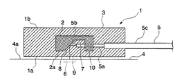
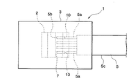
図1は、本発明に係る光路変換部材の一実施形態である光路変換部材1を示す断面図であり、図2は光路変換部材1の平面図である。
光路変換部材1は、光ファイバ5の先端部5aに組み立てられており、基板4に対面して設置される。
基板4としては、光電変換回路、制御処理部、光信号処理回路、光素子駆動回路、その他、電子部品の駆動制御等を行う種々の回路が設けられた回路基板を例示できる。基板4の上面は、光路変換部材1が装着される接合面4aとなっている。
基板4には、光入出端6が設けられている。光入出端6としては、半導体レーザ(例えばレーザダイオード:LD)等の発光素子、あるいは、フォトダイオード(PD)等の受光素子が使用できる。
光入出端6の光軸方向は基板4に対してほぼ垂直となっている。なお、光入出端6の光軸方向は、基板4に対して90°以外の角度で傾斜していてもよい。
FIG. 1 is a cross-sectional view showing an optical path conversion member 1 which is an embodiment of an optical path conversion member according to the present invention, and FIG. 2 is a plan view of the optical path conversion member 1.
The optical path conversion member 1 is assembled at the
Examples of the substrate 4 include a circuit substrate provided with various circuits for performing drive control of electronic components and the like, such as a photoelectric conversion circuit, a control processing unit, an optical signal processing circuit, an optical element driving circuit, and the like. The upper surface of the substrate 4 is a
The substrate 4 is provided with a light input / output end 6. As the light input / output end 6, a light emitting element such as a semiconductor laser (for example, laser diode: LD) or a light receiving element such as a photodiode (PD) can be used.
The optical axis direction of the light input / output end 6 is substantially perpendicular to the substrate 4. The optical axis direction of the light entrance / exit end 6 may be inclined with respect to the substrate 4 at an angle other than 90 °.
光ファイバ5は、例えば多心光ファイバテープ心線であり、先端部5aは例えば光ファイバ5から口出しされた光ファイバ裸線である。図示例では、光ファイバテープ心線から口出しされた複数の先端部5aが、光路変換部材1の底面(装着面1a)に沿って並んで配列されている。
なお、本発明の光路変換部材を適用できる光ファイバは、図示例に限定されず、単心の光ファイバ心線や光ファイバ素線など、各種構成が採用可能である。
光ファイバとしては、例えば全石英製の標準SM型光ファイバあるいはGI型光ファイバが好適であり、標準的な125μm径のものより細径である80μm径のものを使用できる。
以下の説明において、光ファイバ5の先端部5aの先端方向(図1における左方)を前方といい、その逆方向(図1における右方)を後方ということがある。ここでいう前後方向は、光ファイバ5の先端部5aの光軸方向である。なお、先端部5aの光軸方向は光ファイバ5の延在方向である。また、装着面1a側を下といい、反対の面側(上面1b側)を上ということがある。
The
The optical fiber to which the optical path changing member of the present invention can be applied is not limited to the illustrated example, and various configurations such as a single-core optical fiber and an optical fiber can be employed.
As the optical fiber, for example, an all-quartz standard SM type optical fiber or GI type optical fiber is suitable, and an optical fiber having a diameter of 80 μm, which is smaller than the standard 125 μm diameter, can be used.
In the following description, the tip direction (left side in FIG. 1) of the
光路変換部材1は、光路変換体2と、光路変換体2に一体に形成された部材本体3とを備えている。
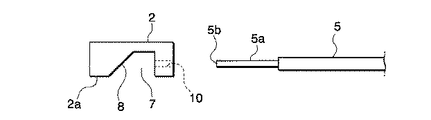
光路変換体2は、例えばブロック状に形成され、その底面2a(基板4側の面)には、反射面形成凹部7(反射面形成空間)が形成されている。図示例では、反射面形成凹部7は、前後方向に対しほぼ垂直な方向(図2における上下方向。図1では紙面垂直方向)に沿う溝状に形成されている。
The optical path conversion member 1 includes an optical
The
図1に示すように、反射面形成凹部7の内面のうち前面は、反射面8となっている。
反射面8は、光ファイバ5の光軸方向(図1における左右方向)および光入出端6の光軸方向(図1における上下方向)に対し傾斜して形成されており、先端部5aの端面5b(先端面)に対面して形成されている。図示例では、反射面8は、反射面形成凹部7の深さ方向に行くに従って後方に傾斜している。
反射面8は、平坦面であってもよいし、レンズとして機能する湾曲凹面であってもよい。レンズとして機能するとは、先端部5a(または光入出端6)からの光を集光して光入出端6(または先端部5a)に向けることをいう。
反射面8は、光路変換部材1を基板4上に配置したときに、光入出端6の上方に位置し、光入出端6の発光面または受光面と対面している。
反射面8には、必要に応じて研磨を施すことで反射効率を高めることができる。なお、反射面8には蒸着などにより金属膜を形成してもよい。
As shown in FIG. 1, the front surface of the inner surface of the reflecting
The reflecting
The reflecting
The
The reflection efficiency can be increased by polishing the reflecting
反射面8は、先端部5aの端面5bから出射した光を反射させて光入出端6に向けるか、または光入出端6から出射した光を反射させて先端部5aの端面5bに向けるようにされ、これにより先端部5aと光入出端6とを光路9によって光接続する。
光路9のうち、反射面8と光入出端6の間の部分は、光入出端6の光軸方向に一致しており、先端部5aの光軸方向に対し傾斜している。図示例では、先端部5aの光軸方向は、回路基板1の延在方向と平行であり、反射面8と光入出端6の間の部分の光路9は、先端部5aの光軸方向に対し垂直である。
The reflecting
A portion of the optical path 9 between the reflecting
光路変換体2の後部には、反射面形成凹部7の後面に開口する光ファイバ挿通孔10が前後方向に沿って形成されている。光ファイバ挿通孔10の後端は光路変換体2の後面で開口している。
光ファイバ挿通孔10は、先端部5aの数と同じ数を図2における上下方向に並べて形成することができる。
光ファイバ挿通孔10には先端部5aが挿通し、端面5b(先端面)が反射面形成凹部7内に配置される。
先端部5aは、接着剤によって光ファイバ挿通孔10の内面に接着されていてもよい。
In the rear part of the
The same number of optical
The optical
The
光路変換体2は、精密成形に適した樹脂が使用できる。例えば、エポキシ樹脂、PPS(ポリフェニレンサルファイド)樹脂、LCP(液晶ポリマー)樹脂などが好適である。光路変換体2は、汎用の樹脂成形法(射出成形、圧縮成形等)により成形できる。
As the
部材本体3は、光路変換体2を含んでインサート成形により一体に形成されている。部材本体3は透明材料からなることが好ましく、例えばポリカーボネイト樹脂、変性ポリオレフィン樹脂、エポキシ樹脂、ポリエチレンイミン(PEI)樹脂、アクリル樹脂などが使用できる。
部材本体3は、少なくとも光路9が通る部分は透明材料からなるように形成することができ、全体が透明材料からなることが好ましい。
The member
The
図示例では、部材本体3は光路変換体2の全体を埋設して形成されているが、光路変換体2の少なくとも一部を含む構成であればよい。例えば、光路変換体2の一部(例えば底面2aが装着面1aに露出していてもよい。
In the illustrated example, the member
図示例では、部材本体3は光ファイバ5の被覆5cの先端部を覆うように形成されている。この構造では、部材本体3を光ファイバ5に対し強固に接合でき、耐久性を高めることができる。
この構造を採用する場合には、被覆5cは耐熱素材で形成することもできる。これによって、部材本体3を成形する際の熱により被覆5cが悪影響を受けるのを防ぐことができる。また、部材本体3に覆われる部分の光ファイバ5を耐熱材または断熱材からなる被覆によりカバーすることもできる。
部材本体3には、基板4に対する位置決めのための嵌合凹凸などの位置決め構造(図示略)を設けることができる。
部材本体3の下面(装着面1a)には、光入出端6に対面する位置に、レンズ手段(図示略)を部材本体3に一体に形成することができる。レンズ手段は、反射面8からの反射光を集光して光入出端6に向けるか、または光入出端6からの出射光を集光して反射面8に向けるものである。
部材本体3の下面(装着面1a)において、光が入出射する部分には、AR(Anti Reflection)コートを形成することができる。
In the illustrated example, the member
When this structure is employed, the
The member
On the lower surface (mounting surface 1 a) of the member
On the lower surface (mounting surface 1a) of the member
次に、光路変換部材1の組み立てについて説明する。
図3および図4に示すように、光ファイバ5の先端部5aを後方から光路変換体2の光ファイバ挿通孔10に挿入し、反射面形成凹部7内に突き出た状態とする。
光路変換体2は、接着剤等によって光ファイバ挿通孔10に固定するのが好ましい。
次いで、図5に示すように、部材本体3に応じた内面形状を有する金型11内に光路変換体2を収容し、金型11内に上記樹脂を充填することによって部材本体3をインサート成形する。
次いで、図6に示すように、金型11を取り外して図1および図2に示す光路変換部材1を得る。
Next, assembly of the optical path conversion member 1 will be described.
As shown in FIGS. 3 and 4, the
The
Next, as shown in FIG. 5, the optical
Next, as shown in FIG. 6, the mold 11 is removed to obtain the optical path changing member 1 shown in FIGS.
光路変換部材1では、部材本体3とは別部材である光路変換体2を使用するため、光路変換体2を部材本体3とは独立に成形できる。光路変換体2は構造が単純であるため、反射面8の形成精度を高めるのが容易となる。
これに対し、光路変換部材全体を一体成形する場合には、他の構造が複雑であると、反射面を精度よく形成するのが難しくなる。他の構造とは、例えば光路変換部材を基板上で位置決めする構造や光ファイバ挿通孔である。
光路変換部材1では、反射面8の高精度に形成できるため、反射面8における反射効率を高めることができ、優れた光特性が得られる。
In the optical path conversion member 1, since the optical
On the other hand, in the case where the entire optical path conversion member is integrally formed, if the other structure is complicated, it is difficult to accurately form the reflecting surface. The other structure is, for example, a structure for positioning the optical path conversion member on the substrate or an optical fiber insertion hole.
In the optical path conversion member 1, since the
光路変換部材1では、特に高い成形精度が要求される部分である光路変換体2(特にその内面の反射面8)と、光路変換体2ほどには高い精度が要求されない他の部分(部材本体3)とを、要求される成形精度に応じた別の金型を使用して作製できるため、光路変換部材全体を一体成形する場合に比べ、製造コストを抑えることができる。
特に、多心化を図る場合には、光ファイバ挿通孔10の数が多くなり高い精度が要求されるため、光路変換部材全体を一体成形する場合は金型の製造コストが非常に高くなるが、光路変換部材1では、金型作製に要するコストを抑制できるため、多心化にも対応できる。
また、光路変換部材1では、光路変換体2と部材本体3とを独立に成形できるため、仕様の変更が容易である。例えば、光路変換体2に関する仕様を変更する場合には、光路変換体2のみを設計変更すればよい。
In the optical path conversion member 1, the optical path conversion body 2 (particularly the reflecting
In particular, in the case of increasing the number of cores, the number of optical fiber insertion holes 10 is increased and high accuracy is required. Therefore, when the entire optical path conversion member is formed integrally, the manufacturing cost of the mold becomes very high. In the optical path conversion member 1, since the cost required for mold production can be suppressed, it is possible to cope with the increase in the number of cores.
Moreover, in the optical path conversion member 1, since the optical
光路変換部材1では、インサート成形を採用するので、部材本体3の成形によって光ファイバ5を固定できる。よって、光ファイバ5を部材本体3に接着固定する工程が不要であり、組み立て工程を簡略化できる。
Since the optical path conversion member 1 employs insert molding, the
また、光路変換部材1では、部材本体3とは別部材である光路変換体2を使用するため、光路変換部材全体が一体である場合に比べ、光ファイバ挿通孔10が短いことから、反射面形成凹部7への先端部5aの突き出し長さを精度よく定めることができる。従って、先端部5aの端面5bと反射面8との距離を正確に設定できる。
Moreover, since the optical path conversion member 1 uses the optical
また、一般的な光路変換部材では、光路変換部材に形成された光ファイバ挿通孔に光ファイバの先端部を挿入し、凹部内に突出させた状態で凹部に接着剤を充填することにより先端部を固定する。このため、接着剤の剥離や接着剤内のマイクロボイド形成が起きることがある。これに対し、光路変換部材1では、インサート成形を採用するので、部材本体3の成形によって光ファイバ5を固定できることから、多量の接着剤は不要であり、このような問題は起こりにくい。
Further, in a general optical path conversion member, the distal end portion is inserted by inserting the distal end portion of the optical fiber into an optical fiber insertion hole formed in the optical path conversion member and filling the concave portion with an adhesive in a state of protruding into the concave portion. To fix. For this reason, peeling of the adhesive or formation of microvoids in the adhesive may occur. On the other hand, since the optical path conversion member 1 employs insert molding, the
1・・・光路変換部材、2・・・光路変換体、3・・・部材本体、4・・・基板、5・・・光ファイバ、5a・・・先端部、5b・・・端面(先端面)、6・・・光入出端、7・・・反射面形成凹部、8・・・反射面、10・・・光ファイバ挿通孔、11・・・金型。 DESCRIPTION OF SYMBOLS 1 ... Optical path conversion member, 2 ... Optical path conversion body, 3 ... Member main body, 4 ... Board | substrate, 5 ... Optical fiber, 5a ... Tip part, 5b ... End surface (tip Surface), 6... Light entry / exit end, 7... Reflection surface forming recess, 8... Reflection surface, 10 .. optical fiber insertion hole, 11.
Claims (3)
前記光ファイバと光入出端のうち一方からの光を他方に向けて反射させてこれらを光接続させる反射面(8)が金型を用いた樹脂成形により形成された光路変換体(2)と、
この光路変換体の少なくとも一部を含んでインサート成形によりこの光路変換体と一体に形成された部材本体(3)とを備え、
前記光路変換体には、前記光路変換部材を前記基板に対面して設置したときに基板側となる面に反射面形成凹部(7)が形成され、前記反射面形成凹部の内面の一方の側に反射面が設けられ、前記反射面に対向するように前記反射面形成凹部の内面の他方の側に前記光ファイバの先端部(5a)の挿通する光ファイバ挿通孔(10)が開口していることを特徴とする光路変換部材。 The optical fiber (5) is assembled at the front end (5a) and is placed facing the substrate (4) provided with a light input / output end (6) having an optical axis inclined with respect to the optical axis direction of the front end. An optical path changing member,
An optical path changer (2) in which a reflecting surface (8) for reflecting light from one of the optical fiber and the light input / output end toward the other and optically connecting them is formed by resin molding using a mold ; ,
A member main body (3) integrally formed with the optical path changing body by insert molding including at least a part of the optical path changing body,
In the optical path changer, a reflection surface forming recess (7) is formed on the surface that becomes the substrate side when the optical path conversion member is placed facing the substrate, and one side of the inner surface of the reflection surface forming recess is formed. The optical fiber insertion hole (10) through which the distal end portion (5a) of the optical fiber is inserted is opened on the other side of the inner surface of the reflection surface forming recess so as to face the reflection surface. optical path conversion member, characterized in that there.
前記光路変換体には、反射面形成凹部(7)が形成されており、前記反射面形成凹部の内面の一方の側に反射面が設けられ、前記反射面に対向するように前記反射面形成凹部の内面の他方の側に前記光ファイバの先端部(5a)の挿通する光ファイバ挿通孔(10)が開口しており、
前記光ファイバ挿通孔に前記光ファイバの先端部を挿通させた前記光路変換体を、前記光路変換部材を前記基板に対面して設置したときに基板側となる面に前記反射面形成凹部が形成されるように金型(11)に入れ、この金型を用いたインサート成形によって、前記部材本体を、前記光路変換体の少なくとも一部を含んで、前記光路変換体と一体となるように形成することを特徴とする光路変換部材の組立方法。 The optical fiber (5) is placed facing a substrate (4) provided with a light input / output end (6) having an optical axis inclined with respect to the optical axis direction of the tip (5a) of the optical fiber (5), and the optical fiber and the optical input / output An optical path changer (2) in which a reflecting surface (8) for reflecting light from one of the ends toward the other and optically connecting them is formed by resin molding using a mold, and a member main body (3) An optical path changing member having
The optical path changer is formed with a reflecting surface forming recess (7), a reflecting surface is provided on one side of the inner surface of the reflecting surface forming recess, and the reflecting surface is formed so as to face the reflecting surface. An optical fiber insertion hole (10) through which the tip (5a) of the optical fiber is inserted is opened on the other side of the inner surface of the recess,
The reflective surface forming recess is formed on the surface that becomes the substrate side when the optical path conversion member having the optical fiber insertion hole inserted through the optical fiber insertion hole is disposed facing the substrate. As described above, the member main body is formed so as to be integrated with the optical path changing body by including at least a part of the optical path changing body by insert molding using the mold (11). A method for assembling an optical path changing member.
Priority Applications (1)
| Application Number | Priority Date | Filing Date | Title |
|---|---|---|---|
| JP2007286482A JP4903112B2 (en) | 2007-11-02 | 2007-11-02 | Optical path changing member and assembling method thereof |
Applications Claiming Priority (1)
| Application Number | Priority Date | Filing Date | Title |
|---|---|---|---|
| JP2007286482A JP4903112B2 (en) | 2007-11-02 | 2007-11-02 | Optical path changing member and assembling method thereof |
Publications (2)
| Publication Number | Publication Date |
|---|---|
| JP2009115919A JP2009115919A (en) | 2009-05-28 |
| JP4903112B2 true JP4903112B2 (en) | 2012-03-28 |
Family
ID=40783151
Family Applications (1)
| Application Number | Title | Priority Date | Filing Date |
|---|---|---|---|
| JP2007286482A Expired - Fee Related JP4903112B2 (en) | 2007-11-02 | 2007-11-02 | Optical path changing member and assembling method thereof |
Country Status (1)
| Country | Link |
|---|---|
| JP (1) | JP4903112B2 (en) |
Families Citing this family (2)
| Publication number | Priority date | Publication date | Assignee | Title |
|---|---|---|---|---|
| JP5652715B2 (en) * | 2011-02-16 | 2015-01-14 | 日立金属株式会社 | Photoelectric conversion device with connector and method for manufacturing photoelectric conversion device with connector |
| JP5491658B2 (en) * | 2013-05-27 | 2014-05-14 | 株式会社フジクラ | Manufacturing method of optical path conversion type optical connector |
Family Cites Families (5)
| Publication number | Priority date | Publication date | Assignee | Title |
|---|---|---|---|---|
| JPH10160959A (en) * | 1996-12-05 | 1998-06-19 | Shinko Electric Ind Co Ltd | Optical multiplexing and demultiplexing structure and optical multiplexing and demultiplexing module using the same |
| JP2002250838A (en) * | 2001-02-26 | 2002-09-06 | Furukawa Electric Co Ltd:The | Optical module, its manufacturing device and method |
| JP2003177286A (en) * | 2001-12-11 | 2003-06-27 | Hosiden Corp | Optical component for bi-directional optical communication |
| JP2003307603A (en) * | 2002-02-15 | 2003-10-31 | Omron Corp | Optical element and optical part using the same |
| JP2005156875A (en) * | 2003-11-25 | 2005-06-16 | Fujikura Ltd | Optical ferrule |
-
2007
- 2007-11-02 JP JP2007286482A patent/JP4903112B2/en not_active Expired - Fee Related
Also Published As
| Publication number | Publication date |
|---|---|
| JP2009115919A (en) | 2009-05-28 |
Similar Documents
| Publication | Publication Date | Title |
|---|---|---|
| JP5250691B2 (en) | Lid | |
| JP5238651B2 (en) | Optical path changing member, optical connection method | |
| JP5127546B2 (en) | Optical connector | |
| JP5564344B2 (en) | Ferrule with optical fiber | |
| TWI507753B (en) | Lens parts and light modules with their light | |
| JP2013235243A (en) | Optical path changing member | |
| EP1857849A1 (en) | Optical transmission module and method of manufacturing the same | |
| US9429717B2 (en) | Ferrule and ferrule with optical fiber | |
| JP5328532B2 (en) | Optical connector | |
| JP4903112B2 (en) | Optical path changing member and assembling method thereof | |
| CN113835165B (en) | Light emitting component, chip, optical module and optical communication equipment | |
| JP2011059487A (en) | Method of manufacturing optical path connector, and the optical path change optical connector | |
| JP5320190B2 (en) | Optical coupling device | |
| JP5131021B2 (en) | Socket for optical connector | |
| JP2006184680A (en) | Optical connector | |
| JP4161899B2 (en) | Optical waveguide module | |
| JP5491658B2 (en) | Manufacturing method of optical path conversion type optical connector | |
| JP2016035484A (en) | Optical module and manufacturing method of optical module | |
| JP7421316B2 (en) | optical module | |
| JP2013137412A (en) | Lens component | |
| CN109891291B (en) | Light path conversion member | |
| JP5282988B2 (en) | Optical connector | |
| JP6268788B2 (en) | Lens parts, optical modules | |
| JP4925584B2 (en) | Optical components | |
| WO2018097072A1 (en) | Optical module and manufacturing method for optical module |
Legal Events
| Date | Code | Title | Description |
|---|---|---|---|
| A621 | Written request for application examination |
Free format text: JAPANESE INTERMEDIATE CODE: A621 Effective date: 20100607 |
|
| A131 | Notification of reasons for refusal |
Free format text: JAPANESE INTERMEDIATE CODE: A131 Effective date: 20110913 |
|
| A977 | Report on retrieval |
Free format text: JAPANESE INTERMEDIATE CODE: A971007 Effective date: 20110914 |
|
| A521 | Request for written amendment filed |
Free format text: JAPANESE INTERMEDIATE CODE: A523 Effective date: 20111114 |
|
| TRDD | Decision of grant or rejection written | ||
| A01 | Written decision to grant a patent or to grant a registration (utility model) |
Free format text: JAPANESE INTERMEDIATE CODE: A01 Effective date: 20111206 |
|
| A01 | Written decision to grant a patent or to grant a registration (utility model) |
Free format text: JAPANESE INTERMEDIATE CODE: A01 |
|
| A61 | First payment of annual fees (during grant procedure) |
Free format text: JAPANESE INTERMEDIATE CODE: A61 Effective date: 20120104 |
|
| FPAY | Renewal fee payment (event date is renewal date of database) |
Free format text: PAYMENT UNTIL: 20150113 Year of fee payment: 3 |
|
| LAPS | Cancellation because of no payment of annual fees |