EP1857841A1 - Light absorbing antireflection structure, optical unit and lens barrel unit including the light absorbing antireflection structure, and optical device including the optical unit and the lens barrel unit - Google Patents
Light absorbing antireflection structure, optical unit and lens barrel unit including the light absorbing antireflection structure, and optical device including the optical unit and the lens barrel unit Download PDFInfo
- Publication number
- EP1857841A1 EP1857841A1 EP07108240A EP07108240A EP1857841A1 EP 1857841 A1 EP1857841 A1 EP 1857841A1 EP 07108240 A EP07108240 A EP 07108240A EP 07108240 A EP07108240 A EP 07108240A EP 1857841 A1 EP1857841 A1 EP 1857841A1
- Authority
- EP
- European Patent Office
- Prior art keywords
- light
- light absorbing
- antireflection structure
- rough surface
- absorbing antireflection
- Prior art date
- Legal status (The legal status is an assumption and is not a legal conclusion. Google has not performed a legal analysis and makes no representation as to the accuracy of the status listed.)
- Withdrawn
Links
Images





Classifications
-
- G—PHYSICS
- G02—OPTICS
- G02B—OPTICAL ELEMENTS, SYSTEMS OR APPARATUS
- G02B1/00—Optical elements characterised by the material of which they are made; Optical coatings for optical elements
- G02B1/10—Optical coatings produced by application to, or surface treatment of, optical elements
- G02B1/11—Anti-reflection coatings
- G02B1/118—Anti-reflection coatings having sub-optical wavelength surface structures designed to provide an enhanced transmittance, e.g. moth-eye structures
-
- G—PHYSICS
- G02—OPTICS
- G02B—OPTICAL ELEMENTS, SYSTEMS OR APPARATUS
- G02B1/00—Optical elements characterised by the material of which they are made; Optical coatings for optical elements
- G02B1/10—Optical coatings produced by application to, or surface treatment of, optical elements
- G02B1/11—Anti-reflection coatings
-
- G—PHYSICS
- G02—OPTICS
- G02B—OPTICAL ELEMENTS, SYSTEMS OR APPARATUS
- G02B5/00—Optical elements other than lenses
- G02B5/003—Light absorbing elements
Definitions
- the present invention relates to a light absorbing antireflection structure, an optical unit and a lens barrel unit including the light absorbing antireflection structure and an optical device including the optical unit and the lens barrel unit.
- a paint film is formed by applying a black material to a substrate surface and then the paint film is dried while a Benard cell is formed, thereby providing a light absorbing member having an increased light absorbing property.
- the present invention has been devised and it is therefore an object of the present invention to provide a light absorbing antireflection structure in which reflection is sufficiently suppressed.
- a light absorbing antireflection structure is directed to a light absorbing antireflection structure for suppressing reflection of light having a wavelength equal to or larger than a predetermined wavelength and absorbing the light of which reflection is suppressed and is characterized in that the light absorbing antireflection structure includes a rough surface having a larger surface roughness than the predetermined wavelength and a plurality of fine concave/convex portions are formed on the rough surface so as to be regularly arranged within a smaller cycle than the predetermined wavelength.
- An optical unit is characterized in that the optical unit includes: an optical system; and a light absorbing antireflection structure for suppressing reflection of light from the optical system and absorbing the light from the optical system, which is placed so that the light from the optical system enters therein, the light absorbing antireflection structure includes a surface which the light from the optical system enters and is formed to be a rough surface having a larger surface roughness than a wavelength of the light from the optical system, and a plurality of fine concave/convex portions are formed on the surface so as to be regularly arranged within a cycle equal to or smaller than the wavelength of the light from the optical system.
- a lens barrel unit is characterized in that the lens barrel unit includes: an optical system; and a lens barrel for storing the optical system therein, suppressing reflection of light from the optical system and absorbing light from the optical system, and the lens barrel is formed so as to include an inner circumference surface of a rough surface having a larger surface roughness than a wavelength of the light from the optical system and a plurality of fine concave/convex portions are formed on the inner circumference surface so as to be regularly arranged within a cycle equal to or smaller than a wavelength of the light from the optical system.
- An optical device is characterized by including the optical unit or the lens barrel unit according to the present invention.
- optical device implemented in accordance with the present invention will be described with reference to an imaging device as an example.
- the optical device according to the present invention is not limited to the imaging device but may be, for example, some other optical device such as an illumination device, a projector and the like.
- FIG. 1 is a schematic view illustrating a configuration of main part of an imaging device 1 according to this embodiment.
- the imaging device 1 includes a device body 3 and a lens barrel unit 2 as an optical unit.
- a lens barrel unit 2 as an optical unit.
- the lens barrel unit 2 may be constructed so as to be removable.
- the lens barrel unit 2 includes a lens barrel 5 having a cylindrical shape (more specifically, a circular cylindrical shape) and an optical system 4 mounted in the lens barrel 5.
- the device body 3 includes an imaging device 6 placed on an optical axis AX of the optical system 4.
- the optical system 4 forms an optical image on an image area of the imaging device 6.
- An optical image formed on an imaging area by the optical system 4 is converted into an electrical signal by the imaging device 6.
- the electrical signal is stored in a memory provided in the device body 3 (or an external memory) and output to some other device via a cable connected to the device body 3.
- the imaging device 6 can be formed of a CCD (charge coupled device), a CMOS (complementary metal-oxide semiconductor) or the like.
- the optical system 4 is not particularly limited to a certain configuration as long as it can preferably form an optical image on an imaging area of the imaging device 6.
- the optical system 4 may include three lenses (or lens groups), i.e., a first lens (group) L1, a second lens (group) L2 and a third lens (group) L3.
- the optical system 4 may have a configuration in which at least one of the three lenses (lens groups) L1, L2 and L3 is displaceable in the optical axis AX direction and focusing and/or scaling are allowed.
- FIG. 2 is a front view of the lens barrel 5.
- FIG. 3 is an enlarged cross-sectional view of part of the lens barrel 5.
- FIG. 4 is a further enlarged cross-sectional view of the part of the lens barrel 5.
- the lens barrel 5 is configured so as to absorb incident light (generally, visible light) into the optical system 4 from an image side.
- incident light generally, visible light
- a ray bundle which enters from the image side into the lens barrel unit 2 at an angle equal to or larger than an overall angle of view of the optical system 4 and stray light caused by reflection at a surface of a lens or the like constituting the optical system 4 are absorbed by the lens barrel 5. Accordingly, the generation of a ghost image, a flare or the like is suppressed and thus the imaging device 1 of this embodiment has a high optical performance.
- a light absorbing material for example, a dye and a pigment
- the lens barrel 5 may be formed of a light absorbing material.
- a black dye for example, Plast Black 9850 and 8970 available from Arimoto Chemical Co., Ltd.
- a plurality of coloring agents such as cyan, magenta and yellow, a carbon black or the like
- a main body into which such a dye or a pigment is dispersedly mixed may be, for example, glass, resin such as acryl resin and poly carbonate resin (preferably, resin of which glass transition temperature is 90 °C or more and 170 °C or less) or glass fiber containing resin.
- the lens barrel 5 preferably contains an antistatic material.
- the lens barrel 5 preferably has an excellent light fastness (specifically, for ultraviolet light).
- a plurality of fine concave/convex portions 11 for suppressing reflection of light are formed in an inner circumference surface 10 of the lens barrel 5. More specifically, the plurality of fine concave/convex portions 11 are formed so as to be regularly arranged within a smaller cycle than a predetermined wavelength (in this case, a smaller cycle than a wavelength of incident light from the optical system 4, i.e., a wavelength of visible light and, more preferably, a smallest wavelength of incident light from the optical system 4) throughout the inner circumference surface 10 of the lens barrel 5.
- a predetermined wavelength means to be a wavelength of light of which reflection is desired to be suppressed, or a wavelength of light of which reflection should be suppressed.
- SWS fine concave/convex portions 11 are regularly arranged.
- SWS fine concave/convex portions 11
- each of the fine concave/convex portions 11 may be an approximately conical concave or convex (of which a top portion may be chamfered or R-chamfered), a prismoid concave or convex or a filiform concave or a filiform convex of which a cross-sectional shape is triangular, trapezoidal, rectangular or the like (of which edge portions may be R-chamfered).
- a cycle i.e., a distance between top points of adjacent ones of the fine concave/convex portions 11 when viewed from the top in the normal direction of a reference plane of the inner circumference surface 10 formed to be a rough surface
- a "reference plane” means to be a plane obtained by cutting off the fine concave/convex portions 11 and a roughness shape as high-frequency components.
- a "roughness shape” means to be a shape obtained by cutting off the fine concave/convex portions 11 as high-frequency components from a shape of the inner circumference surface 10 including the fine concave/convex portions 11 (hereafter, the shape of the inner circumference surface 10 including the fine concave/convex portions 11 will be referred to as merely a "shape of the inner circumference surface 10").
- a height (strictly speaking, defined to be a distance from the reference plane of the inner circumference surface 10, which is formed to be a rough surface, in the normal direction of the reference plane) of each of the fine concave/convex portions 11 is preferably equal to or larger than 0.4 times as large as a wavelength of incident light into the lens barrel unit 2 from an image side, more preferably equal to or larger than the wavelength, and even more preferably equal to or larger than three times as large as the wavelength. Strictly speaking, as in this embodiment, assume that incident light has a wavelength width.
- the cycle of the fine concave/convex portions 11 is preferably equal to or smaller than a smallest wavelength of incident light and the height of each of the fine concave/convex portions 11 is preferably equal to or larger than 0.4 times as large as the largest wavelength of incident light (more preferably the same as the smallest wavelength and even more preferably equal to or larger than three times as large as the largest wavelength).
- the fine concave/convex portions 11 do not have to exhibit antireflection effect for all incident light.
- a wavelength of incident light is in a wide wavelength range including ultraviolet light, near-ultraviolet light, visible light, near-infrared light and infrared light but the imaging device 6 is capable of detecting only light in the range from 400 nm to 1000 nm, it is not always required to suppress reflection of light having a smaller wavelength than 400 nm and light having a larger wavelength than 1000 nm.
- the cycle of the fine concave/convex portions 11 is preferably equal to or smaller than 400 nm.
- the height of each of the fine concave/convex portions 11 is preferably equal to or larger than 0.4 times as large as 1000 nm, i.e., 400 nm or more.
- the fine concave/convex portions 11 may be formed so that the height of the fine concave/convex portions 11 differs between different parts (for example, each having a size of 1 mm squares) of the inner circumference surface 10. However, in view of simplification of formation, the fine concave/convex portions 11 are preferably formed so that respective heights of the fine concave/convex portions 11 in the different parts are approximately the same.
- the fine concave/convex portions 11 include conical/pyramidal concaves and conical/pyramid convexes
- the fine concave/convex portions 11 are preferably formed so that a central axis of each of cones or pyramids, connecting a center point of a base and a top point of each of the cones or the pyramids, is approximately in parallel to central axises of other cones or pyramids.
- fabrication of the lens barrel 5 by injection molding is simple.
- the fine concave/convex portions 11 include filiform concaves and filiform convexes each having a triangular cross section
- the plurality of fine concave/convex portions 11 are preferably formed so that a center axis of each of filiform portions, connecting respective center points of a top and a base of each of the filiform portions, is approximately in parallel to center axises of other filiform portions in each part (for example, having a size of 1 mm squares) of the inner circumference surface 10.
- the lens barrel 5 absorbs incident light (strictly speaking, light having a wavelength of which reflection should be suppressed) into the lens barrel unit 2 from an image side and the plurality of fine concave/convex portions 11 for suppressing reflection of such light are formed in the inner circumference surface 10, so that reflection of light at the inner circumference surface 10 of the lens barrel 5 is largely reduced.
- incident light strictly speaking, light having a wavelength of which reflection should be suppressed
- the plurality of fine concave/convex portions 11 for suppressing reflection of such light are formed in the inner circumference surface 10, so that reflection of light at the inner circumference surface 10 of the lens barrel 5 is largely reduced.
- the inner circumference surface 10 is a smooth surface, regular reflection at the inner circumference surface 10 can not be sufficiently suppressed.
- FIG. 6 is a graph showing intensity of reflected light of incident light at an incident angle of 45 degrees.
- the inner circumference surface 10 of the lens barrel 5 is formed so as to be a rough surface having a larger surface roughness than a wavelength of incident light. More specifically, the inner circumference surface 10 is formed so that a surface roughness in terms of maximum height roughness Rz defined in ISO4287:1997 (JIS B0601: 2001) is larger than a wavelength of incident light.
- Rz maximum height roughness
- the inner circumference surface 10 in which the fine concave/convex portions 11 are formed is formed so as to be a rough surface having a larger surface roughness than a wavelength of incident light, so that a reflection coefficient of incident light at a relatively large incident angle can be reduced.
- this effect will be described in detail with reference to FIG. 5 and FIG. 7 .
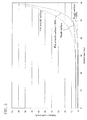
- FIG. 7 is a graph showing the correlation between incident angle and reflection coefficient in surfaces in which the fine concave/convex portions 11 are formed.
- ⁇ in FIG. 7 denotes an angle between a normal vector N 2 of a tangent plane 13 of a roughness shape of the inner circumference surface 10 and a normal vector N 1 of a reference plane 12 of the inner circumference surface 10 (see FIG. 9).
- ⁇ is 0 degrees (in other words, the inner circumference surface 10 is a smooth surface).
- incident light has a large angle, i.e., a larger angle than 50 degrees or an even larger angle, i.e., a larger angle than 70 degrees, even with the fine concave/convex portions 11 formed on the smooth surface, a reflection coefficient tends to be increased as an incident angle increases.
- the light absorbing antireflection structure in the case of a light absorbing antireflection structure (so-called "black body"), incident light is not always light at a relatively small incident angle, e.g., an angle of 45 degrees or less. Therefore, it is preferable that the light absorbing antireflection structure has a configuration which suppresses reflection of incident light at a relatively large incident angle. The problem of suppressing reflection of light at a relatively large incident angle is unique to the light absorbing antireflection structure.
- the inner circumference surface 10 is a rough surface and therefore an incident angle is substantially small in average, compared to the case where the inner circumference surface 10 is a smooth surface. Accordingly, as shown in FIG. 5, in this embodiment, reflection of incident light at a relatively large incident angle can be effectively suppressed. Also, as shown in FIG. 5, when the SWS is formed on a smooth surface, a relatively high antireflection effect for incident light at a relatively small incident angle can be achieved. However, a sufficient antireflection effect for incident light at a relatively large incident angle can not be achieved. That is, when the SWS is formed on a smooth surface, it is difficult to sufficiently suppress the dependency of reflection coefficient to angle.
- an angle ( ⁇ ) between a normal vector N 2 of a tangent plane 13 of a roughness shape of the inner circumference surface 10 (more specifically, a tangent plane of a shape, i.e., a roughness shape obtained by cutting off the fine concave/convex portions 11 as high-frequency components from a shape of the inner circumference surface 10 including the fine concave/convex portions 11) and a normal vector N 1 of the reference plane 12 of the inner circumference surface 10 is 5 degrees or less.
- the percentage of an area of part in which ⁇ is 5 degrees or less per unit area is preferably less than 80%. In other words, the percentage of an area per unit area of part in which ⁇ is preferably 5 degrees or more is 20% or more. Moreover, the percentage of an area per unit area of part in which ⁇ is 10 degrees or less is preferably less than 90%. In other words, the percentage of an area per unit area of part in which ⁇ is 10 degrees or more is 10% or more. In such case, compared to the case where the fine concave/convex portions 11 are formed on a smooth surface, a reflection coefficient of light at an incident angle of 89 degrees can be reduced by about 30% or more.
- the percentage of the area per unit area of the part in which ⁇ is 5 degrees or less is preferably less than 50%. In other words, the percentage of the area per unit area of the part in which ⁇ is 5 degrees or more is preferably 50% or more. Moreover, the percentage of the area per unit area of the part in which ⁇ is 10 degrees or less is preferably less than 80%. In other words, the percentage of the area per unit area of the part in which ⁇ is 10 degrees or more is preferably 20% or more. In such case, compared to the case where the fine concave/convex portions 11 are formed on a smooth surface, the reflection coefficient of light at an incident angle of 89 degrees can be reduced by about 50% or more.
- the percentage of the area per unit area of the part in which ⁇ is 5 degrees or less is preferably less than 30%. In other words, the percentage of the area per unit area of the part in which ⁇ is 5 degrees or more is preferably 70% or more. Moreover, the percentage of the area per unit area of the part in which ⁇ is preferably 10 degrees or less is preferably less than 50%. In other words, the percentage of the area per unit area of the part in which ⁇ is 10 degrees or more is preferably 50% or more. In such case, compared to the case where the fine concave/convex portions 11 are formed on a smooth surface, the reflection coefficient of light at an incident angle of 89 degrees can be reduced by about 70% or more.
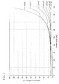
- FIG. 8 is a graph showing the correlation between ⁇ ave and reflection coefficient.
- ⁇ ave is preferably 5 degrees or more.
- the reflection coefficient of light at an incident angle of 89 degrees can be reduced by about 30% or more.
- ⁇ ave is 10 degrees or more.
- the reflection coefficient of light at an incident angle of 89 degrees can be reduced by about 50% or more.
- ⁇ ave is 15 degrees or more.
- the reflection coefficient of light at an incident angle of 89 degrees can be reduced by about 30% or more.
- a peak (i.e., a value of ⁇ which is most frequently included) of a ⁇ distribution is preferably larger than 0 degrees.
- the peak is more preferably 2 degrees or more, or even more preferably 5 degrees or more.
- part in which ⁇ is larger than 90 degrees does not exist.
- the inner circumference surface 10 is substantially formed of a plane having a roughness shape of ⁇ ⁇ 90 degrees.
- the part in which ⁇ is larger than 90 degrees exists, it is difficult to form the fine concave/convex portions 11 on a surface facing to a depression portion 17.
- the inner circumference surface 10 is preferably formed so that diffracted light is not generated from incident light.
- the roughness shape of the inner circumference surface 10 is preferably formed so as to be aperiodic.
- a peak width for example, a width of a peak at a half of a height of the peak
- W 2 of a peak 16 for the roughness shape of the inner circumference surface 10 is preferably larger than a peak width W 1 of a peak 15 for the fine concave/convex portions 11.
- the roughness shape of the inner circumference surface 10 is formed within a cycle, there might be cases where diffracted light is generated from incident light into the inner circumference surface 10 and a ghost image, a flare and the like are generated due to the diffracted light.
- the generation of diffracted light and also the generation of a ghost image, a flare and the like can be effectively suppressed.
- the inner circumference surface 10 is preferably formed so that a distribution width of cycles standardized with a center cycle (which is most frequently included in the inner circumference surface 10) of the roughness shape is equal to or larger than 0.4 times as large as the center cycle. If the distribution width of the cycles standardized with the center cycle is smaller than 0.4 times as large as the center cycle, in the inner circumference surface 10, part of a diffraction angle in which a second-order diffracted light exists and another part of a diffraction angle in which a third-order diffracted light exists are isolated from each other, so that unevenness in the generated diffracted light might be generated.
- the distribution width of the cycles standardized with the center cycle is preferably equal to or larger than 2/3 times as large as the center cycle.
- the lens barrel 5 does not have to be a single unit body, but may be formed of a plurality of components.
- the SWS is formed throughout the inner circumference surface 10 of the lens barrel 5 .
- the SWS does not have to be provided throughout the inner circumference surface 10 of the lens barrel 5 , but may be formed only in necessary part.
- other part of the inner circumference surface 10 may be a rough surface having the same surface roughness as the surface roughness of the part in which the SWS is provided or may be a smooth surface having a smaller surface roughness than the surface roughness of the part in which the SWS is provided.
- some other antireflection structure including a multilayer film of a film having a relatively low reflection coefficient and a film having a relatively large reflection coefficient may be formed in part in which the SWS is not formed. That is, as long as at least part of a surface of a light absorbing member which light enters is formed to be a rough surface and the SWS is formed on the rough surface, a light absorbing antireflection structure according to the present invention is not limited at all. Moreover, even in the part in which the SWS is formed, a height and a cycle (pitch) of the SWS may be adjusted as necessary.
- the SWS structure may be formed on surfaces of other members such as the lenses (lens groups) L1, L2 and L3 constituting the optical system 4 as well as on the inner circumference surface 10 of the lens barrel 5.
- the lens barrel 5 when the lens barrel 5 has a light absorbing property, there might be cases where, after using the imaging device 1 for a long time, the lens barrel 5 generates heat. Furthermore, when heat generation becomes stronger or a high temperature state continues for a long time, there might be cases where the lens barrel 5 is deteriorated by heat.
- a space may be formed in the lens barrel 5 and a refrigerant may be enclosed therein.
- the internal space in the lens barrel 5 may be connected to a radiator and the like so that the refrigerant therein is circulated to sequentially cool down the lens barrel 5 .
- the refrigerant, an antifreeze liquid containing polyethylene glycol and water, air, a compound liquid containing alcohol and water, or the like can be used.
- the light absorbing antireflection structure (lens barrel 5 ) formed so as to have a cylindrical shape has been described particularly in details.
- a shape of the above-described lens barrel 5 is not limited to the above-described shape but may be formed into various different shapes such as a flat plane shape, a sheet shape, a truncated cone or a prismoid shape in which a through hole passing through in the height direction is formed, and the like.
- a surface of the light absorbing antireflection structure in which the SWS is not formed may be formed on an adhesion surface or a cohesion surface.
- the light absorbing antireflection structure may be used for an image sensor such as a charge-coupled device (CCD) and the like, an optical measuring device such as a power meter, an energy meter, a reflection coefficient measuring device and the like , a microlens array, a photo disc and the like.
Landscapes
- Physics & Mathematics (AREA)
- General Physics & Mathematics (AREA)
- Optics & Photonics (AREA)
- Lens Barrels (AREA)
- Optical Elements Other Than Lenses (AREA)
- Surface Treatment Of Optical Elements (AREA)
Applications Claiming Priority (1)
| Application Number | Priority Date | Filing Date | Title |
|---|---|---|---|
| JP2006134906A JP2007304466A (ja) | 2006-05-15 | 2006-05-15 | 光吸収性反射防止構造体、それを備えた光学ユニット及びレンズ鏡筒ユニット、並びにそれらを備えた光学装置 |
Publications (1)
| Publication Number | Publication Date |
|---|---|
| EP1857841A1 true EP1857841A1 (en) | 2007-11-21 |
Family
ID=38268705
Family Applications (1)
| Application Number | Title | Priority Date | Filing Date |
|---|---|---|---|
| EP07108240A Withdrawn EP1857841A1 (en) | 2006-05-15 | 2007-05-15 | Light absorbing antireflection structure, optical unit and lens barrel unit including the light absorbing antireflection structure, and optical device including the optical unit and the lens barrel unit |
Country Status (4)
| Country | Link |
|---|---|
| US (1) | US20070291386A1 (https=) |
| EP (1) | EP1857841A1 (https=) |
| JP (1) | JP2007304466A (https=) |
| CN (1) | CN101082680B (https=) |
Cited By (3)
| Publication number | Priority date | Publication date | Assignee | Title |
|---|---|---|---|---|
| EP1947500A1 (en) * | 2007-01-17 | 2008-07-23 | Fujinon Corporation | Optical element and optical unit |
| US11493669B2 (en) | 2016-11-21 | 2022-11-08 | Otsuka Techno Corporation | Anti-reflective body, camera unit, mobile device, and method for manufacturing anti-reflective body |
| EP4564065A1 (en) * | 2023-12-01 | 2025-06-04 | Canon Kabushiki Kaisha | Structural body for absorbing light, member, optical apparatus, and method of manufacturing structural body |
Families Citing this family (18)
| Publication number | Priority date | Publication date | Assignee | Title |
|---|---|---|---|---|
| WO2007148718A1 (ja) * | 2006-06-21 | 2007-12-27 | Panasonic Corporation | 光学部材、それを備えた光学系、光学ユニット、及び光学装置 |
| WO2009031299A1 (ja) * | 2007-09-03 | 2009-03-12 | Panasonic Corporation | 反射防止構造体、光学ユニット及び光学装置 |
| DE102008033383A1 (de) * | 2008-07-16 | 2010-01-21 | Osram Gesellschaft mit beschränkter Haftung | Halterungsrahmen für ein optisches Element |
| KR20100032767A (ko) * | 2008-09-18 | 2010-03-26 | 제일모직주식회사 | 마이크로렌즈 패턴과 엠보 패턴을 구비하는 확산필름 및 그제조방법 |
| GB2465607A (en) * | 2008-11-25 | 2010-05-26 | St Microelectronics | CMOS imager structures |
| JP2011100020A (ja) * | 2009-11-06 | 2011-05-19 | Fujifilm Corp | レンズ鏡筒 |
| JP2015018005A (ja) | 2011-11-11 | 2015-01-29 | パナソニック株式会社 | レンズ鏡筒 |
| JP5837892B2 (ja) * | 2013-01-23 | 2015-12-24 | 東芝テック株式会社 | 結像素子アレイ及び画像形成装置 |
| DE102013106392B4 (de) * | 2013-06-19 | 2017-06-08 | Fraunhofer-Gesellschaft zur Förderung der angewandten Forschung e.V. | Verfahren zur Herstellung einer Entspiegelungsschicht |
| US20180074229A1 (en) * | 2015-03-30 | 2018-03-15 | Scivax Corporation | Anti-reflective structure |
| US10473879B2 (en) * | 2016-08-01 | 2019-11-12 | Samsung Electro-Mechanics Co., Ltd. | Lens module and camera module including same |
| WO2019087439A1 (ja) * | 2017-11-02 | 2019-05-09 | 国立研究開発法人産業技術総合研究所 | 光吸収体の製造方法 |
| TWI689750B (zh) * | 2019-03-20 | 2020-04-01 | 大立光電股份有限公司 | 光學鏡頭及電子裝置 |
| WO2021000202A1 (zh) * | 2019-06-30 | 2021-01-07 | 瑞声光学解决方案私人有限公司 | 镜头模组和电子设备 |
| JP7459656B2 (ja) * | 2020-05-25 | 2024-04-02 | 王子ホールディングス株式会社 | 反射防止構造体 |
| US20220381952A1 (en) * | 2021-05-28 | 2022-12-01 | Hewlett-Packard Development Company, L.P. | Head mounted displays with an anti-reflection layer |
| CN113640906A (zh) * | 2021-07-09 | 2021-11-12 | 中国科学院近代物理研究所 | 一种近完美光吸收体及其普适性的制备方法 |
| CN115425370B (zh) * | 2022-09-30 | 2023-09-22 | 厦门海辰储能科技股份有限公司 | 连接片、电池、电池包和用电设备 |
Citations (5)
| Publication number | Priority date | Publication date | Assignee | Title |
|---|---|---|---|---|
| US6359735B1 (en) * | 1997-03-04 | 2002-03-19 | Fraunhofer Gesellschaft Zur Forderung Der Angewandten Forschung E.V. | Antireflective coating and method of manufacturing same |
| US20030180476A1 (en) * | 2002-03-25 | 2003-09-25 | Sanyo Electric Co., Ltd. | Antireflective member and electronic equipment using same |
| US20050093210A1 (en) * | 2003-10-29 | 2005-05-05 | Matsushita Electric Industrial Co., Ltd. | Method for producing optical element having antireflection structure, and optical element having antireflection structure produced by the method |
| WO2005116695A1 (en) * | 2004-05-27 | 2005-12-08 | Matsushita Electric Industrial Co., Ltd. | Light-absorbing member |
| JP2006113561A (ja) * | 2004-09-16 | 2006-04-27 | Fuji Photo Film Co Ltd | 光散乱性フィルムの製造方法、該光散乱性フィルムを用いた偏光板、該偏光板を用いた液晶表示装置 |
Family Cites Families (5)
| Publication number | Priority date | Publication date | Assignee | Title |
|---|---|---|---|---|
| CA2029665C (en) * | 1989-11-17 | 1996-12-03 | Shoichi Nagai | Shaped articles and method of making same |
| WO2002093534A1 (fr) * | 2001-05-16 | 2002-11-21 | Bridgestone Corporation | Fenetre assurant la transmission de la lumiere et une protection contre les ondes electromagnetiques |
| JP2003107205A (ja) * | 2001-09-28 | 2003-04-09 | Fuji Photo Film Co Ltd | 防眩層を含む光学フイルム及び画像表示装置 |
| JP4740603B2 (ja) * | 2004-01-23 | 2011-08-03 | 富士フイルム株式会社 | 反射防止フィルムの製造方法 |
| EP1723448A1 (en) * | 2004-03-12 | 2006-11-22 | Matsushita Electric Industrial Co., Ltd. | Light-absorbing member |
-
2006
- 2006-05-15 JP JP2006134906A patent/JP2007304466A/ja active Pending
-
2007
- 2007-05-15 US US11/798,533 patent/US20070291386A1/en not_active Abandoned
- 2007-05-15 EP EP07108240A patent/EP1857841A1/en not_active Withdrawn
- 2007-05-15 CN CN2007101049890A patent/CN101082680B/zh not_active Expired - Fee Related
Patent Citations (5)
| Publication number | Priority date | Publication date | Assignee | Title |
|---|---|---|---|---|
| US6359735B1 (en) * | 1997-03-04 | 2002-03-19 | Fraunhofer Gesellschaft Zur Forderung Der Angewandten Forschung E.V. | Antireflective coating and method of manufacturing same |
| US20030180476A1 (en) * | 2002-03-25 | 2003-09-25 | Sanyo Electric Co., Ltd. | Antireflective member and electronic equipment using same |
| US20050093210A1 (en) * | 2003-10-29 | 2005-05-05 | Matsushita Electric Industrial Co., Ltd. | Method for producing optical element having antireflection structure, and optical element having antireflection structure produced by the method |
| WO2005116695A1 (en) * | 2004-05-27 | 2005-12-08 | Matsushita Electric Industrial Co., Ltd. | Light-absorbing member |
| JP2006113561A (ja) * | 2004-09-16 | 2006-04-27 | Fuji Photo Film Co Ltd | 光散乱性フィルムの製造方法、該光散乱性フィルムを用いた偏光板、該偏光板を用いた液晶表示装置 |
Non-Patent Citations (1)
| Title |
|---|
| KANAMORI Y ET AL: "BROADBAND ANTIREFLECTION GRATINGS FABRICATED UPON SILICON SUBSTRATES", OPTICS LETTERS, OSA, OPTICAL SOCIETY OF AMERICA, WASHINGTON, DC, US, vol. 24, no. 20, 15 October 1999 (1999-10-15), pages 1422 - 1424, XP000873713, ISSN: 0146-9592 * |
Cited By (4)
| Publication number | Priority date | Publication date | Assignee | Title |
|---|---|---|---|---|
| EP1947500A1 (en) * | 2007-01-17 | 2008-07-23 | Fujinon Corporation | Optical element and optical unit |
| US7672064B2 (en) | 2007-01-17 | 2010-03-02 | Fujinon Corporation | Optical element and optical unit |
| US11493669B2 (en) | 2016-11-21 | 2022-11-08 | Otsuka Techno Corporation | Anti-reflective body, camera unit, mobile device, and method for manufacturing anti-reflective body |
| EP4564065A1 (en) * | 2023-12-01 | 2025-06-04 | Canon Kabushiki Kaisha | Structural body for absorbing light, member, optical apparatus, and method of manufacturing structural body |
Also Published As
| Publication number | Publication date |
|---|---|
| CN101082680A (zh) | 2007-12-05 |
| JP2007304466A (ja) | 2007-11-22 |
| US20070291386A1 (en) | 2007-12-20 |
| CN101082680B (zh) | 2012-06-13 |
Similar Documents
| Publication | Publication Date | Title |
|---|---|---|
| EP1857841A1 (en) | Light absorbing antireflection structure, optical unit and lens barrel unit including the light absorbing antireflection structure, and optical device including the optical unit and the lens barrel unit | |
| JP2007304466A5 (https=) | ||
| CN100427971C (zh) | 光吸收构件 | |
| JP6525078B2 (ja) | 光学フィルタおよび撮像装置 | |
| US8529075B2 (en) | Antireflection structure, optical unit, and optical device | |
| EP1667231B1 (en) | Method of manufacturing a SOLID-STATE IMAGING DEVICE | |
| WO2005088355A1 (en) | Light-absorbing member | |
| US8259394B2 (en) | Antireflection structure and optical device including the same | |
| WO2008001662A1 (en) | Optical member and optical device comprising the same | |
| US20140029103A1 (en) | Optical black surface | |
| US7102824B2 (en) | Optical element for efficient sensing at large angles of incidence | |
| US20110299169A1 (en) | Antireflection structure and optical device including the same | |
| JP2009128522A (ja) | 光吸収性反射防止構造体、それを備えた光学ユニット及びレンズ鏡筒ユニット、並びにそれらを備えた光学装置 | |
| US20230239557A1 (en) | Camera apparatus and electronic device | |
| TW202142908A (zh) | 鏡筒 | |
| EP3933459B1 (en) | Optical element, camera module, terminal and method for processing optical element | |
| US11703660B2 (en) | Optical imaging lens | |
| JP2004214470A (ja) | 集光式太陽光発電装置 | |
| WO2026062039A1 (en) | Hybrid refractive and meta-optical lens camera module | |
| CN119717224A (zh) | 光学成像系统 | |
| JP2017120327A (ja) | レンズシート、撮像モジュール、撮像装置 |
Legal Events
| Date | Code | Title | Description |
|---|---|---|---|
| PUAI | Public reference made under article 153(3) epc to a published international application that has entered the european phase |
Free format text: ORIGINAL CODE: 0009012 |
|
| AK | Designated contracting states |
Kind code of ref document: A1 Designated state(s): AT BE BG CH CY CZ DE DK EE ES FI FR GB GR HU IE IS IT LI LT LU LV MC MT NL PL PT RO SE SI SK TR |
|
| AX | Request for extension of the european patent |
Extension state: AL BA HR MK YU |
|
| 17P | Request for examination filed |
Effective date: 20080521 |
|
| 17Q | First examination report despatched |
Effective date: 20080630 |
|
| AKX | Designation fees paid |
Designated state(s): DE FR GB |
|
| RAP1 | Party data changed (applicant data changed or rights of an application transferred) |
Owner name: PANASONIC CORPORATION |
|
| STAA | Information on the status of an ep patent application or granted ep patent |
Free format text: STATUS: THE APPLICATION IS DEEMED TO BE WITHDRAWN |
|
| 18D | Application deemed to be withdrawn |
Effective date: 20131120 |